

General Description
The DS4302 is a 5-bit digital-to-analog converter (DAC)
with three programmable digital outputs. The DS4302
communicates through a 2-wire, SMBus™-compatible,
serial interface. The tiny 8-pin µSOP package is ideal
for use in space-constrained applications.
Applications
CCFL Backlight Brightness Control
Power-Supply Calibration
Features
♦ SO Package is a Drop-In Replacement for the
MPS1251 and MPS1252
♦ Single 5-Bit DAC (32 Steps)
♦ 0V to 2V and 0V to 1.9V Versions
♦ Three Programmable Digital Outputs
♦ SMBus-Compatible Serial Interface
♦ 4.5V to 5.5V Supply Voltage Range
♦ 8-Pin SO and 8-Pin µSOP Packages
♦ Industrial Temperature Range: -40°C to +85°C
DS4302
2-Wire, 5-Bit DAC with Three Digital Outputs
______________________________________________ Maxim Integrated Products 1
TOP VIEW
P1
P2GND
1
2
87V
CC
P0SDA
V
OUT
SCL
SO/µSOP
3
4
6
5
DS4302
Pin Configuration
Ordering Information
Rev 1; 6/04
For pricing, delivery, and ordering information, please contact Maxim/Dallas Direct! at
1-888-629-4642, or visit Maxim’s website at www.maxim-ic.com.
Add “/T&R” for tape-and-reel orders.
*Contact factory for availability.
SMBus is a trademark of Intel Corp.
PART
V
OUT
RANGE
TOP
BRAND
PIN-
PACKAGE
DS4302Z-020
4302B 8 SO
DS4302Z-019*
4302A 8 SO
DS4302U-020
4302B 8 µSOP
DS4302U-019*
4302A 8 µSOP
Pin Description
PIN
FUNCTION
1 SCL Serial Clock Input. 2-wire clock input.
2 SDA
Serial Data Input/Output. Bidirectional,
2-wire data pin.
3V
OUT
DAC Output Voltage
4 GND Ground
5P2
6P1
7P0
Programmable Digital Output
8VCCPower-Supply Input
查询DS4302供应商
0V to 2.0V
0V to 1.9V
0V to 2.0V
0V to 1.9V
NAME
DS4302
2-Wire, 5-Bit DAC with Three Digital Outputs
2 _____________________________________________________________________
ABSOLUTE MAXIMUM RATINGS
RECOMMENDED DC OPERATING CONDITIONS
(TA= -40°C to +85°C)
Stresses beyond those listed under “Absolute Maximum Ratings” may cause permanent damage to the device. These are stress ratings only, and functional
operation of the device at these or any other conditions beyond those indicated in the operational sections of the specifications is not implied. Exposure to
absolute maximum rating conditions for extended periods may affect device reliability.
Voltage Range on VCC, SDA, and SCL Pins
Relative to Ground.............................................-0.5V to +6.0V
Operating Temperature Range ...........................-40°C to +85°C
Storage Temperature Range .............................-55°C to +125°C
Soldering Temperature.....See IPC/JEDEC J-STD-020A Specification
PARAMETER
CONDITIONS
UNITS
Supply Voltage V
CC
(Note 1) 4.5 5.5 V
Input Logic 1 (SDA, SCL) V
IH
2.0
V
Input Logic 0 (SDA, SCL) V
IL
0.8 V
DC ELECTRICAL CHARACTERISTICS
(VCC= +4.5V to 5.5V, TA= -40°C to +85°C.)
X = Don’t care.
SYMBOL
Standby Current I
Input Leakage I
SDA Low-Level Output Voltage V
P0, P1, P2 Low-Level Output
Voltage
P0, P1, P2 High-Level Output
Voltage
V
OUT
V
OUT
V
OUT
V
OUT
Power-On Reset 1.7 V
Settling Time 10 µs
D/A Output Levels 32 steps
PARAMETER SYMBOL CONDITIONS MIN TYP MAX UNITS
STBY
OL1
V
OL2
V
OH
Maximum Level (-020) VCC = 5.0V, Data = 00000XXX (Note 3) 1.925 2.0 2.075 V
Minimum Level (-020) VCC = 5.0V, Data = 11111XXX 0.0 0.05 0.1 V
Maximum Level (-019) VCC = 5.0V, Data = 00000XXX (Note 3) 1.825 1.9 1.975 V
Minimum Level (-019) VCC = 5.0V, Data = 11111XXX 0.0 0.05 0.1 V
(Notes 2, 3) 200 300 µA
(Note 4) -1.0 +1.0 µA
L
3mA sink current 0.0 0.4
6mA sink current 0.0 0.6
(Note 1)
4mA sink
(Note 1)
4mA source
MIN TYP MAX
V
+ 0.3
CC
GND - 0.3
+0.4V V
- 0.4V V
V
CC
V
DS4302
2-Wire, 5-Bit DAC with Three Digital Outputs
_____________________________________________________________________ 3
PARAMETER
SYMBOL
CONDITIONS
MIN
TYP
MAX
UNITS
SCL Clock Frequency f
SCL
0 400 kHz
Bus Free Time Between STOP
and START Conditions
t
BUF
1.3 µs
Low Period of SCL t
LOW
1.3 µs
High Period of SCL t
HIGH
0.6 µs
Data Hold Time
0 0.9 µs
Data Setup Time
100 ns
Start Setup Time t
SU:STA
0.6 µs
SDA and SCL Rise Time t
R
(Note 5)
300 ns
SDA and SCL Fall Time t
F
(Note 5)
300 ns
Stop Setup Time
0.6 µs
SDA and SCL Capacitive
Loading
C
B
(Note 5) 400 pF
AC ELECTRICAL CHARACTERISTICS (Figure 3)
(VCC= +4.5V to 5.5V, TA= -40°C to +85°C, timing referenced to V
IL(MAX)
and V
IH(MIN)
.)
Note 1: All voltages referenced to ground.
Note 2: I
STBY
specified for the inactive state measured with SDA = SCL = VCCand with V
OUT
, P0, P1, and P2 floating.
Note 3: No load on V
OUT
.
Note 4: The DS4302 will not obstruct the SDA and SCL lines if V
CC
is switched off as long as the voltages applied to these inputs
does not violate their min and max input-voltage levels.
Note 5: C
B
—total capacitance of one bus line in picofarads.
t
HD:DAT
t
SU:DAT
t
SU:STO
20 + 0.1C
20 + 0.1C
B
B

DS4302
2-Wire, 5-Bit DAC with Three Digital Outputs
4 _____________________________________________________________________
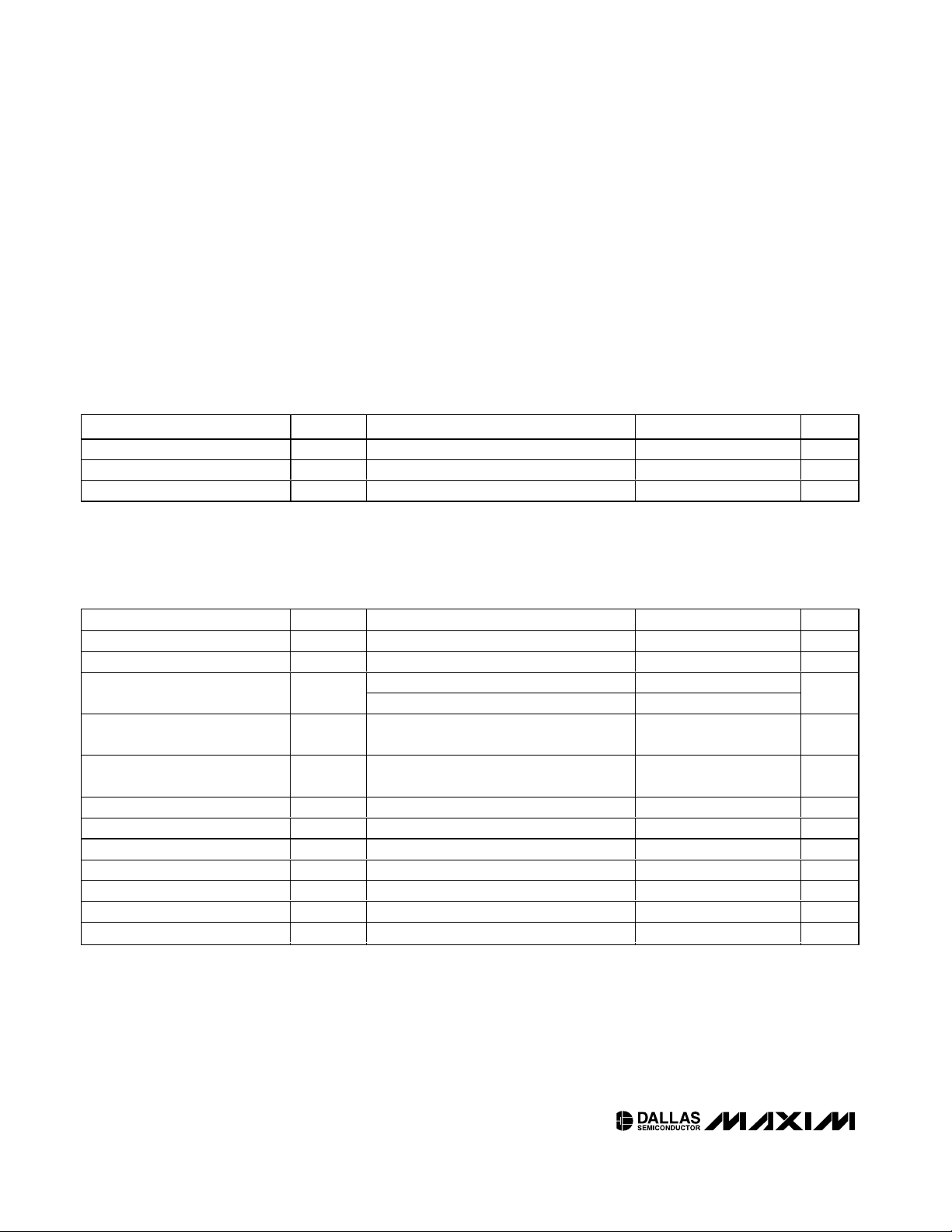
Typical Operating Characteristics
(VCC= +5.0V, TA = +25°C.)
STANDBY SUPPLY CURRENT
vs. SUPPLY VOLTGE
DS4302 toc01
SUPPLY VOLTAGE (V)
STANDBY SUPPLY CURRENT (µA)
5.255.004.75
50
100
150
200
250
300
0
4.50 5.50
OUTPUTS UNLOADED
SDA = SCL = V
CC
STANDBY SUPPLY CURRENT
vs. TEMPERATURE
DS4302 toc02
TEMPERATURE (°C)
STANDBY SUPPLY CURRENT (µA)
20
40
60
0-20
50
100
150
200
250
300
0
-40
80
OUTPUTS UNLOADED
SDA = SCL = V
CC
= 5.0V
SUPPLY CURRENT
vs. SCL FREQUENCY
DS4302 toc03
SCL FREQUENCY (kHz)
SUPPLY CURRENT (µA)
300200100
50
100
150
200
250
300
0
0400
OUTPUTS UNLOADED
SDA = V
CC
V
OUT
vs. DAC SETTING
DS4302 toc04
DAC SETTING (dec)
V
OUT
(V)
30252015105
0.5
1.0
1.5
2.0
0
0
DS4302-020 VERSION
V
OUT
vs. SUPPLY VOLTAGE
DS4302 toc05
SUPPLY VOLTAGE (V)
V
OUT
(V)
5.255.004.75
1.95
2.00
2.05
2.10
1.90
4.50 5.50
V
CC
= SDA = SCL
V
OUT
PERCENT CHANGE FROM +25°C
vs. TEMPERATURE
DS4302 toc06
TEMPERATURE (°C)
V
OUT
PERCENT CHANGE (%)
80
60
40
200-20
-0.5
0
0.5
1.0
-1.0
-40
V
CC
= SDA = SCL

DS4302
2-Wire, 5-Bit DAC with Three Digital Outputs
_____________________________________________________________________ 5
Functional Diagram
2-WIRE
INTERFACE
GND
5-BIT
DAC
V
OUT
BANDGAP
REFERENCE
SCL
SDA
MSB
LSB
DATA BYTE REGISTER
DAC VALUE
P0P2 P1
P0
V
CC
V
CC
OUTPUT CELL
P1
P2
V
CC
OUTPUT CELL
OUTPUT CELL
BUFFER
DS4302

DS4302
Detailed Description
The DS4302 contains a 5-bit DAC and three programmable digital outputs. The DAC setting and the programmed output levels are contained in a 1-byte data
word that defaults to 00h on power-up (see Figure 1 for
data byte configuration). The upper 5 MSbits of the byte
set the DAC and control the voltage produced on V
OUT
.
A setting of 1111 1XXX sets the minimum output voltage
from the DAC while a setting of 0000 0XXX sets the maximum output voltage from the DAC. The three LSbits of
the data byte control the three output pins, P0, P1, and
P2. Setting any of these control bits to a 0 pulls the corresponding outputs low and setting the bits to a 1 pulls the
outputs high.
The DS4302 communicates through a 2-wire (SMBuscompatible) digital interface and has a 2-wire address of
58h. Write and read operations are used to access the
DAC and output settings. Each operation begins with a
2-wire START condition, consists of three bytes, and
ends with a 2-wire STOP condition (see Figure 2). Using
the write operation, the 2-wire master can program the
5-bit DAC to adjust the voltage on VOUT and set the
level of the three output pins: P0, P1, and P2. The read
operation is used to recall the programmed settings.
2-Wire Definitions
The following terminology is commonly used to
describe 2-wire data transfers.
Master Device: The master device controls the slave
devices on the bus. The master device generates SCL
clock pulses, START, and STOP conditions.
Slave Devices: Slave devices send and receive data
at the master’s request.
Bus Idle or Not Busy: Time between STOP and START
conditions when both SDA and SCL are inactive and in
their logic-high states. When the bus is idle, it initiates a
low-power mode for slave devices.
START Condition: A START condition is generated by
the master to initiate a new data transfer with a slave.
Transitioning SDA from high to low while SCL remains
high generates a START condition. See Figure 3 for
applicable timing.
STOP Condition: A STOP condition is generated by the
master to end a data transfer with a slave. Transitioning
SDA from low to high while SCL remains high generates
a STOP condition. See Figure 3 for applicable timing.
Bit Write: Transitions of SDA must occur during the low
state of SCL. The data on SDA must remain valid and
unchanged during the entire high pulse of SCL plus the
setup and hold time requirements (see Figure 3). Data is
shifted into the device during the rising edge of the SCL.
2-Wire, 5-Bit DAC with Three Digital Outputs
6 _____________________________________________________________________
DATA BYTE
MSB
DAC VALUE P0P2 P1
Figure 1. Data Byte Configuration
Figure 2. 2-Wire Communication Examples
S
P
A
START
8-BITS ADDRESS OR DATA
STOP
ACK
WHITE BOXES INDICATE THE MASTER IS
CONTROLLING SDA
SHADED BOXES INDICATE THE SLAVE IS
CONTROLLING SDA
WRITE A SINGLE BYTE
AAh
READ A SINGLE BYTE 00h59h
58h
COMMUNICATIONS KEY
S
XXXXXXXX
0101100 0 A
DATA BYTE
A
P
NOTES:
1) ALL BYTES ARE SENT MOST SIGNIFICANT BIT FIRST.
2) THE FIRST BYTE SENT AFTER A START CONDITION IS
ALWAYS THE SLAVE ADDRESS FOLLOWED BY THE
READ/WRITE BIT.
00001111
S 01011001A A
DATA BYTE
A
P
00000000
A

Bit Read: At the end a write operation, the master must
release the SDA bus line for the proper amount of setup
time (see Figure 3) before the next rising edge of SCL
during a bit read. The device shifts out each bit of data
on SDA at the falling edge of the previous SCL pulse
and the data bit is valid at the rising edge of the current
SCL pulse. Remember that the master generates all
SCL clock pulses including when it is reading bits from
the slave.
Acknowledgement (ACK): An Acknowledgement
(ACK) is always the 9th bit transmitted during a byte
transfer. The device receiving data (the master during a
read or the slave during a write operation) performs an
ACK by transmitting a zero during the 9th bit. For timing, see Figure 3. An ACK is the acknowledgement that
the device is properly receiving data.
Byte Write: A byte write consists of 8 bits of information transferred from the master to the slave (most significant bit first) plus a 1-bit acknowledgement from the
slave to the master. The 8 bits transmitted by the master are done according to the bit write definition and the
acknowledgement is read using the bit read definition.
Byte Read: A byte read is an 8-bit information transfer
from the slave to the master plus a 1-bit ACK from the
master to the slave. The 8 bits of information that are
transferred (most significant bit first) from the slave to
the master are read by the master using the bit read
definition above, and the master transmits an ACK
using the bit write definition to receive additional data
bytes. The master must ACK the last byte read to terminated communication so the slave returns control of
SDA to the master.
Slave Address and the R/W Bit: Each slave on the
2-wire bus responds to a slave addressing byte sent
immediately following a START condition. The slave
address byte contains the slave address and the R/W
bit. The slave address (see Figure 4) is the most significant 7 bits and the R/W bit is the least significant bit.
The DS4302’s slave address is 0101100X (binary),
where X is the R/W bit. If the R/W bit is zero
(01011000), the master will write data to the slave. If the
R/W is a one (01011001), the master will read data from
the slave.
Memory Address: During a 2-wire write operation, the
master must transmit a memory address to identify the
memory location where the slave is to store the data.
The memory address is the second byte transmitted
during a write or read operation following the slave
address byte (R/W=0). For a write operation, the memory address is 10101010 (AAh) and for a read operation, the memory address is 00000000 (00h).
DS4302
2-Wire, 5-Bit DAC with Three Digital Outputs
_____________________________________________________________________ 7
7-BIT SLAVE ADDRESS
MOST
SIGNIFICANT
BIT
DETERMINES
READ OR WRITE
R/W0011010
Figure 4. Slave Address and the R/WBit
Figure 3. 2-Wire Timing Diagram
SDA
SCL
STOP
NOTE: TIMING IS REFERENCE TO V
IL(MAX)
AND V
IH(MIN)
.
START
t
BUF
t
LOW
t
R
t
F
t
SU:DAT
t
SU:STA
t
HD:STA
t
SU:STO
t
SP
REPEATED
START
t
HD:STA
t
HD:DAT
t
HIGH

DS4302
2-Wire, 5-Bit DAC with Three Digital Outputs
Maxim cannot assume responsibility for use of any circuitry other than circuitry entirely embodied in a Maxim product. No circuit patent licenses are
implied. Maxim reserves the right to change the circuitry and specifications without notice at any time.
8 _____________________Maxim Integrated Products, 120 San Gabriel Drive, Sunnyvale, CA 94086 408-737-7600
© 2004 Maxim Integrated Products Printed USA is a registered trademark of Maxim Integrated Products.
DALLAS is a registered trademark of Dallas Semiconductor Corporation.
2-Wire Communication
Writing to a Slave: The master must generate a START
condition, write the slave address (R/W = 0), write the
memory address, write the byte of data, and generate a
STOP condition. Remember the master must read the
slave’s acknowledgement during all byte-write operations. See Figure 2 for the write command example.
Reading from a Slave: To read from the slave, the
master generates a START condition, writes the slave
address with R/W = 1, receives an ACK from the slave,
reads a memory address of 00h from the slave, sends
an ACK to the slave, reads the data byte, then sends
an ACK to indicate the end of the transfer, and generates a STOP condition. See Figure 2 for the read command example.
Application Information
Power-Supply Decoupling
To achieve the best results when using the DS4302,
decouple the power supply with a 0.01µF or a 0.1µF
capacitor. Use high-quality, ceramic, surface-mount
capacitors, and mount the capacitors as close as possible to the VCCand GND pins of the DS4302 to minimize lead inductance.
SDA and SCL Pullup Resistors
Pullup resistor values for SDA and SCL should be chosen to ensure that the rise and fall times listed in the AC
electrical characteristics are within specification.
Package Information
For the latest package outline information, go to
www.maxim-ic.com/DallasPackInfo
.
Chip Information
TRANSISTOR COUNT: 2428
SUBSTRATE CONNECTED TO GROUND
 Loading...