

Page 1
___________________________________ 概述
DS4302 是一款5位数模转换器 (DAC),提供三路可编程数
字输出。DS4302通过2线、SMBusTM兼容的串行接口进行
通信。微型8引脚µSOP封装,使其适合空间受限的应用。
___________________________________ 应用
CCFL背光亮度控制
电源校准
___________________________________ 特性
♦ SO封装可直接替换MPS1251和MPS1252
♦ 单路5位DAC (32级)
♦ 0V至2V和0V 至1.9V两种版本
♦ 三路可编程数字输出
♦ SMBus兼容的串行接口
♦ 电源电压范围:4.5V至5.5V
♦ 8引脚SO封装及8引脚µSOP封装
♦ 工业级温度范围: -40°C至+85°C
DS4302
2线、5位DAC,提供三路数字输出
______________________________________________ Maxim Integrated Products 1
_______________________________ 引脚配置
_______________________________ 定购信息
Rev 1; 6/04
若需卷带包装请加注“/T&R”。
*
供货信息请与厂商联系。
SMBus是 Intel Corp.的商标。
_______________________________ 引脚说明
本文是Maxim 正式英文资料的译文,Maxim不对翻译中存在的差异或由此产生的错误负责。请注意译文中可能存在文字组织或
翻译错误,如需确认任何词语的准确性,请参考 Maxim提供的英文版资料。
索取免费样品和最新版的数据资料,请访问Maxim的主页:www.maxim-ic.com.cn。
引脚
名称 功能
串行时钟输入。2线时钟输入。
串行数据输入/输出。双向、2线数据
引脚。
DAC输出电压
地
可编程数字输出
电源输入
V
PART
DS4302Z-020 0V to 2.0V 4302B 8 SO
DS4302Z-019* 0V to 1.9V 4302A 8 SO
DS4302U-020 0V to 2.0V 4302B 8 µSOP
DS4302U-019* 0V to 1.9V 4302A 8 µSOP
OUT
RANGE
TOP
BRAND
PINPACKAGE
PIN NAME FUNCTION
1 SCL Serial Clock Input. 2-wire clock input.
2 SDA
3V
4 GND Ground
5P2
6P1
7P0
8VCCPower-Supply Input
Serial Data Input/Output. Bidirectional,
2-wire data pin.
DAC Output Voltage
OUT
Programmable Digital Output
TOP VIEW
V
SCL
OUT
1
2
3
4
DS4302
SO/µSOP
87V
6
5
CC
P0SDA
P1
P2GND
Page 2
DS4302
2线、5位DAC,提供三路数字输出
2 _____________________________________________________________________
ABSOLUTE MAXIMUM RATINGS
RECOMMENDED DC OPERATING CONDITIONS
(TA= -40°C to +85°C)
Stresses beyond those listed under “Absolute Maximum Ratings” may cause permanent damage to the device. These are stress ratings only, and functional
operation of the device at these or any other conditions beyond those indicated in the operational sections of the specifications is not implied. Exposure to
absolute maximum rating conditions for extended periods may affect device reliability.
Voltage Range on VCC, SDA, and SCL Pins
Relative to Ground.............................................-0.5V to +6.0V
Operating Temperature Range ...........................-40°C to +85°C
Storage Temperature Range .............................-55°C to +125°C
Soldering Temperature ....See IPC/JEDEC J-STD-020A Specification
DC ELECTRICAL CHARACTERISTICS
(VCC= +4.5V to 5.5V, TA= -40°C to +85°C.)
X = Don’t care.
PARAMETER SYMBOL CONDITIONS MIN TYP MAX UNITS
Supply Voltage V
Input Logic 1 (SDA, SCL) V
Input Logic 0 (SDA, SCL) V
CC
(Note 1) 4.5 5.5 V
IH
IL
2.0 V
GND - 0.3 0.8 V
+ 0.3 V
CC
PARAMETER SYMBOL CONDITIONS MIN TYP MAX UNITS
Standby Current I
Input Leakage I
SDA Low-Level Output Voltage V
P0, P1, P2 Low-Level Output
Voltage
P0, P1, P2 High-Level Output
Voltage
V
Maximum Level (-020) VCC = 5.0V, Data = 00000XXX (Note 3) 1.925 2.0 2.075 V
OUT
V
Minimum Level (-020) VCC = 5.0V, Data = 11111XXX 0.0 0.05 0.1 V
OUT
V
Maximum Level (-019) VCC = 5.0V, Data = 00000XXX (Note 3) 1.825 1.9 1.975 V
OUT
V
Minimum Level (-019) VCC = 5.0V, Data = 11111XXX 0.0 0.05 0.1 V
OUT
Power-On Reset 1.7 V
Settling Time 10 µs
D/A Output Levels 32 steps
STBY
OL1
V
OL2
V
OH
(Notes 2, 3) 200 300 µA
(Note 4) -1.0 +1.0 µA
L
3mA sink current 0.0 0.4
6mA sink current 0.0 0.6
(Note 1)
4mA sink
(Note 1)
4mA source
- 0.4V V
V
CC
+0.4V V
V
Page 3
DS4302
2线、5位DAC,提供三路数字输出
_____________________________________________________________________ 3
AC ELECTRICAL CHARACTERISTICS (Figure 3)
(VCC= +4.5V to 5.5V, TA= -40°C to +85°C, timing referenced to V
IL(MAX)
and V
IH(MIN)
.)
Note 1: All voltages referenced to ground.
Note 2: I
STBY
specified for the inactive state measured with SDA = SCL = VCCand with V
OUT
, P0, P1, and P2 floating.
Note 3: No load on V
OUT
.
Note 4: The DS4302 will not obstruct the SDA and SCL lines if V
CC
is switched off as long as the voltages applied to these inputs
does not violate their min and max input-voltage levels.
Note 5: C
B
—total capacitance of one bus line in picofarads.
PARAMETER SYMBOL CONDITIONS MIN TYP MAX UNITS
SCL Clock Frequency f
Bus Free Time Between STOP
and START Conditions
Low Period of SCL t
High Period of SCL t
Data Hold Time t
Data Setup Time t
Start Setup Time t
SDA and SCL Rise Time t
SDA and SCL Fall Time t
Stop Setup Time t
SDA and SCL Capacitive
Loading
SCL
t
BUF
LOW
HIGH
HD:DAT
SU:DAT
SU:STA
R
F
SU:STO
C
B
(Note 5) 20 + 0.1C
(Note 5) 20 + 0.1C
(Note 5) 400 pF
0 400 kHz
1.3 µs
1.3 µs
0.6 µs
00.9µs
100 ns
0.6 µs
0.6 µs
B
B
300 ns
300 ns
Page 4
DS4302
2线、5位DAC,提供三路数字输出
4 _____________________________________________________________________
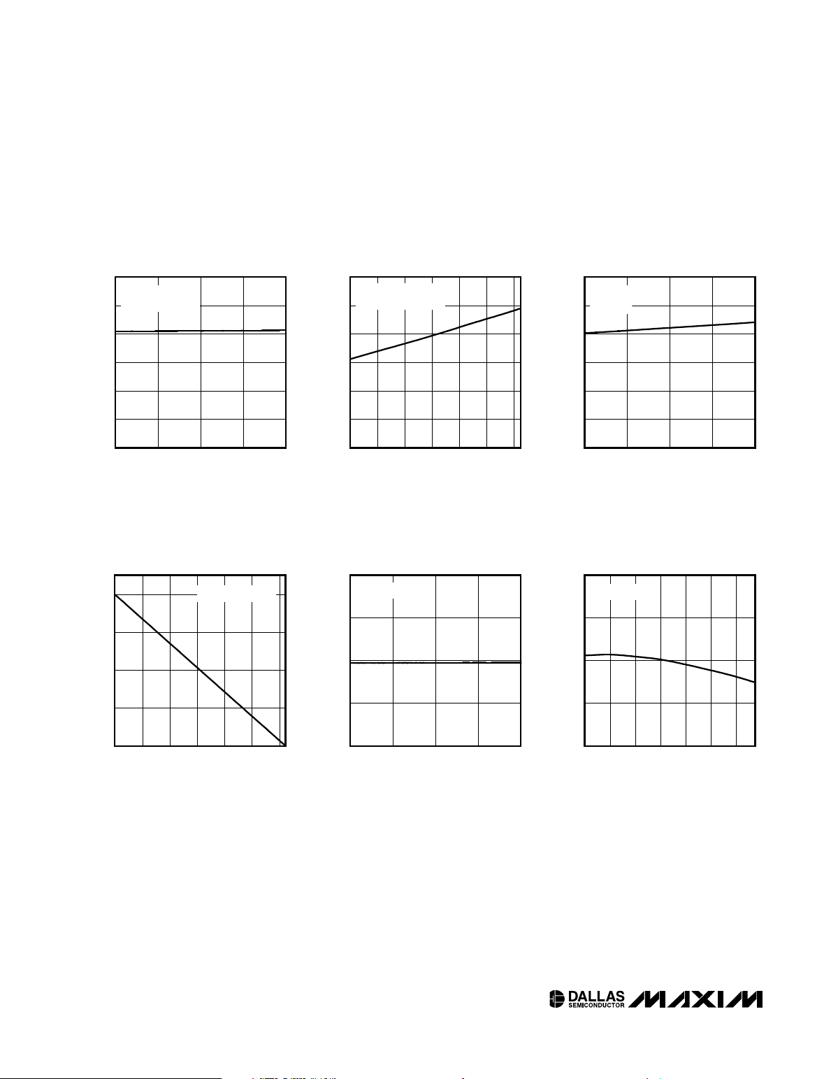
_______________________________________________________________________典型工作特性
(VCC= +5.0V, TA = +25°C.)
STANDBY SUPPLY CURRENT
vs. SUPPLY VOLTGE
DS4302 toc01
SUPPLY VOLTAGE (V)
STANDBY SUPPLY CURRENT (µA)
5.255.004.75
50
100
150
200
250
300
0
4.50 5.50
OUTPUTS UNLOADED
SDA = SCL = V
CC
STANDBY SUPPLY CURRENT
vs. TEMPERATURE
DS4302 toc02
TEMPERATURE (°C)
STANDBY SUPPLY CURRENT (µA)
20
40
60
0-20
50
100
150
200
250
300
0
-40
80
OUTPUTS UNLOADED
SDA = SCL = V
CC
= 5.0V
SUPPLY CURRENT
vs. SCL FREQUENCY
DS4302 toc03
SCL FREQUENCY (kHz)
SUPPLY CURRENT (µA)
300200100
50
100
150
200
250
300
0
0400
OUTPUTS UNLOADED
SDA = V
CC
V
OUT
vs. DAC SETTING
DS4302 toc04
DAC SETTING (dec)
V
OUT
(V)
30252015105
0.5
1.0
1.5
2.0
0
0
DS4302-020 VERSION
V
OUT
vs. SUPPLY VOLTAGE
DS4302 toc05
SUPPLY VOLTAGE (V)
V
OUT
(V)
5.255.004.75
1.95
2.00
2.05
2.10
1.90
4.50 5.50
V
CC
= SDA = SCL
V
OUT
PERCENT CHANGE FROM +25°C
vs. TEMPERATURE
DS4302 toc06
TEMPERATURE (°C)
V
OUT
PERCENT CHANGE (%)
80
60
40
200-20
-0.5
0
0.5
1.0
-1.0
-40
V
CC
= SDA = SCL
Page 5

DS4302
2线、5位DAC,提供三路数字输出
_____________________________________________________________________ 5
___________________________________________________________________________功能框图
DATA BYTE REGISTER
SDA
SCL
V
OUT
V
GND
CC
V
CC
2-WIRE
INTERFACE
DS4302
BUFFER
MSB
DAC VALUE
5-BIT
DAC
BANDGAP
REFERENCE
LSB
P0P2 P1
OUTPUT CELL
V
OUTPUT CELL
OUTPUT CELL
CC
P0
P1
P2
Page 6

DS4302
_______________________________ 详细说明
DS4302包含一个5位DAC以及三路可编程数字输出。DAC
设置及可编程输出电平包含在一个单字节数据字内,上电
时该字节缺省值为 00h (参考图1中的数据字节配置)。字节
的高5位用来设置DAC并控制V
OUT
的输出电压。1111 1XXX
用来设置DAC的最小输出电压,0000 0XXX用来设置DAC
的最大输出电压。数据字节的低3位用来控制三个输出引
脚P0、P1和P2的状态。这三个控制位的任意一位设置为0
时,将使对应输出拉低;任意一位设置为1时,将使对应
输出拉高。
DS4302 通过2线 (SMBus兼容) 数字接口进行通信,且具
有58h的2线地址。使用读、写操作访问DAC并设置输出。
每次操作从2线START条件开始,包括三个字节,并终止
于一个 2线STOP条件 (见图2)。2线主机可利用写操作对
5位DAC进行编程,以调整V
OUT
电压,设置三个输出引
脚P0、P1和P2的电平。读操作用于返回已编程的设定值。
2线定义
一般使用下列术语来描述2线数据传输。
主机设备:主机设备控制总线上的从机设备。主机设备
产生SCL时钟脉冲、START条件及STOP条件。
从机设备:从机设备在主机的要求下发送或接收数据。
总线空闲或非忙状态:位于STOP条件和START条件之间
的时间段,此时SDA和SCL均为无效和逻辑高状态。当总
线空闲时,将为从机设备启动低功耗模式。
START条件:由主机产生START条件,以启动新的数据
传输。SCL保持高电平时,SDA从高到低的跳变将产生一
个START条件。正确的时序请参考图3。
STOP条件:由主机产生STOP条件,以结束与从机的数
据传输。SCL保持高电平时,SDA从低到高的跳变将产生
一个STOP条件。正确的时序请参考图3。
写位:SDA的跳变必须发生在SCL为低电平期间。在整个
SCL的高脉冲期间,并在建立时间和保持时间要求的范围
内 (参见图3),SDA 上的数据必须保持恒定有效。数据在
SCL的上升沿移入设备。
2线、5位DAC,提供三路数字输出
6 _____________________________________________________________________
图1. 数据字节配置
图2. 2线通信举例
DATA BYTE
DAC VALUE P0P2 P1
MSB
COMMUNICATIONS KEY
S
START
P
STOP
XXXXXXXX
WRITE A SINGLE BYTE
S
0101100 0 A
READ A SINGLE BYTE 00h59h
S 01011001A A
A
ACK
8-BITS ADDRESS OR DATA
58h
WHITE BOXES INDICATE THE MASTER IS
CONTROLLING SDA
SHADED BOXES INDICATE THE SLAVE IS
CONTROLLING SDA
AAh
A
00001111
000 00000
DATA BYTE
DATA BYTE
NOTES:
1) ALL BYTES ARE SENT MOST SIGNIFICANT BIT FIRST.
2) THE FIRST BYTE SENT AFTER A START CONDITION IS
ALWAYS THE SLAVE ADDRESS FOLLOWED BY THE
READ/WRITE BIT.
A
P
P
A
Page 7

读位:在写操作结束时,主机必须释放SDA总线,在下
一个 SCL上升沿之前 (读位时) 保持适当的建立时间 (见
图3)。设备在SCL脉冲的下降沿移出每一位SDA数据,且
数据位在随后的SCL脉冲的上升沿有效。要记住主机产生
所有的SCL时钟脉冲,即使是从从机读数据位时。
应答 (ACK):应答 (ACK) 总是字节传输过程中发送的第
9位。接收数据的设备 (读操作中的主机或写操作中的从
机) 通过在第9位发送零来执行一个ACK操作。时序参考
图3。ACK是设备正常接收数据的应答信号。
写字节:写字节操作包括由主机传输到从机 (最高位在前
面) 的8位信息和由从机到主机的1位应答。主机按写位
定义发送8位数据,按照读位定义读取应答信息。
读字节:读字节操作由从机传输到主机的8位信息和一位
从主机到从机的ACK组成。主机使用上面的读位定义读
取从从机传输 (最高位在前面) 到主机的8位信息,然后
主机按照位定义发送一个ACK,以接收额外的数据字节。
终止通信,主机读取最后一个字节后必须发送ACK,以
便从机将SDA的控制权返回到主机。
从机地址及 R/W位: 2线总线上的每个从机均响应 START
条件后发送的从机寻址字节。从机寻址字节包括从机地
址和 R/W位。从机地址 (见图4) 为高7位,R/W位为最低
有效位。
DS4302 的从机地址为0101100X (二进制),其中X为R/W
位。若R/W位为零 (01011000),则主机将向从机写入数据。
若R/W位为1 (01011001),则主机将从从机读取数据。
存储器地址:在2线写操作期间,为确定从机存储数据的
存储器位置,主机必须发送一个存储器地址。存储器地
址为写操作或读操作期间紧随从机地址字节 (R/W= 0) 之
后所发送的第二个字节。写操作时存储器地址为10101010
(AAh),读操作时存储器地址为00000000 (00h)。
DS4302
2线、5位DAC,提供三路数字输出
_____________________________________________________________________ 7
图4. 从机地址及R/W位
图3. 2线时序图
SDA
SCL
STOP
t
BUF
START
t
HD:STA
t
LOW
t
R
t
HD:DAT
t
F
t
HIGH
t
SU:DAT
REPEATED
START
t
SU:STA
t
HD:STA
t
SP
t
SU:STO
NOTE: TIMING IS REFERENCE TO V
IL(MAX)
AND V
IH(MIN)
.
7-BIT SLAVE ADDRESS
R/W0011010
MOST
SIGNIFICANT
BIT
DETERMINES
READ OR WRITE
Page 8

DS4302
2线、5位DAC,提供三路数字输出
Maxim不对 Maxim产品以外的任何电路使用负责,也不提供其专利许可。Maxim保留在任何时间、没有任何通报的前提下修改产品资料和规格的权利。
8 _____________________Maxim Integrated Products, 120 San Gabriel Drive, Sunnyvale, CA 94086 408-737-7600
© 2004 Maxim Integrated Products Printed USA
是
Maxim Integrated Products, Inc.
的注册商标。
是
Dallas Semiconductor Corporation
的注册商标。
2线通信
向从机写数据:主机必须产生一个START条件、写从机
地址 (R/W = 0)、写存储器地址、写数据字节、并产生
STOP条件。记住在所有写字节操作期间,主机必须读取
从机的应答信息。关于写命令的例子可参见图2。
从从机读取数据:为了从从机读取数据,主机必须产生
一个START条件、写从机地址 (R/W = 1)、接收从机的
ACK、读取从机的存储器地址00h、向从机发送ACK、读
取数据字节,接着发送ACK以指示传输结束,并产生
STOP条件。关于读命令的例子可参见图2。
_______________________________ 应用信息
电源去耦
为在使用DS4302时达到最佳效果,要用一个0.01µF或
0.1µF电容对电源去耦。使用高品质、陶瓷、表面贴装的
电容,并将电容安装在尽可能靠近DS4302 VCC和GND引
脚的位置,从而最大程度降低引线电感。
SDA及SCL上拉电阻
选择SDA和SCL上拉电阻的阻值时,要保证上升和下降时
间符合AC Electical Characteristics给出的指标。
_______________________________ 封装信息
如需最近的封装外型信息,请查询
www.maxim-ic.com.c
n/DallasPackInfo。
_______________________________ 芯片信息
TRANSISTOR COUNT: 2428
SUBSTRATE CONNECTED TO GROUND
MAXIM北京办事处
北京 8328信箱 邮政编码 100083
免费电话:800 810 0310
电话:010-6201 0598
传真:010-6201 0298
 Loading...