

Page 1
General Description
The DS4301 is a single 32-position linear digital potentiometer with 200kΩ end-to-end resistance. The wiper
setting is stored in EEPROM, so the DS4301 powers up
with the last stored setting. The position of the wiper is
controlled through a simple three-terminal
increment/decrement interface. The DS4301 is ideal for
white LED backlight brightness control. Its 8-pin µSOP
package, 2.4V to 5.5V supply range, and 200kΩ end-
to-end resistance are especially suited for portable,
battery-powered applications such as cellular telephones and PDAs.
Applications
White LED Backlight Brightness Control
Portable Battery-Powered Devices such as PDAs
and Cellular Phones
Any Application that Requires a Small, Low-Cost
NV Potentiometer
Features
♦ Single, 32-Position, 200kΩ Linear Nonvolatile (NV)
Potentiometer Ideal for Battery-Powered
Applications
♦ Three-Terminal Increment/Decrement Interface to
Adjust Wiper Position
♦ Wide Voltage Supply Range (2.4V to 5.5V)
♦ Command-Initiated NV Wiper Storage
♦ Operates Over the Industrial Temperature Range
(-40°C to +85°C)
♦ Available in 8-Pin µSOP
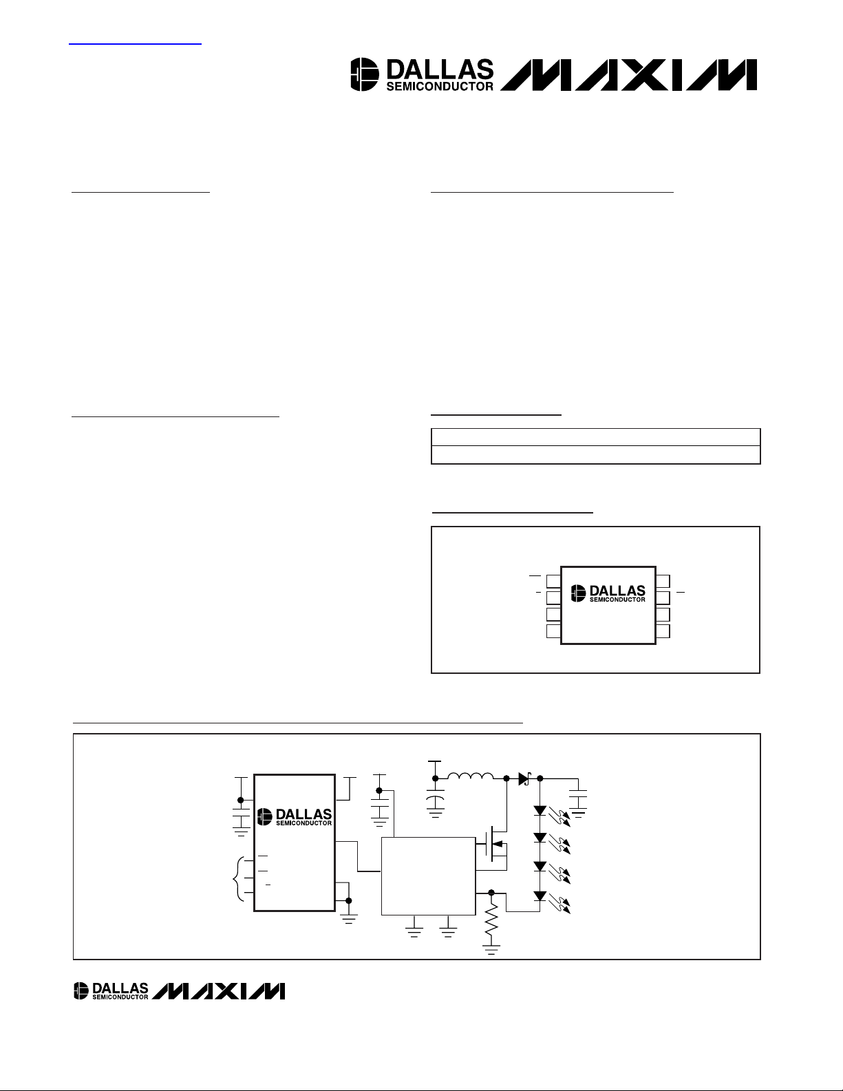
DS4301
Nonvolatile, 32-Position Digital Potentiometer
______________________________________________ Maxim Integrated Products 1
1
2
3
4
8
7
6
5
V
CC
CS
L
WGND
H
U/D
INC
µSOP
TOP VIEW
DS4301
Pin Configuration
Ordering Information
V
CC
V
CC
V
CC
V
CC
V
REF
V
CC
ADJ
EXT
CS
FB
GND PGND
W
H
L
WHITE LED
CURRENT
REGULATOR
R
FB
WHITE
LEDs
10µH
MBR0540
1µF
1µF
10µF
GND
CS
INC
U/D
0.1µF
CONTROL
INTERFACE
DS4301
Typical Operating Circuit
Rev 0; 8/03
For pricing, delivery, and ordering information, please contact Maxim/Dallas Direct! at
1-888-629-4642, or visit Maxim’s website at www.maxim-ic.com.
PART TEMP RANGE PIN-PACKAGE
DS4301U-200 -40°C to +85°C
8 µSOP (118 mil)
查询DS4301供应商
Page 2
DS4301
Nonvolatile, 32-Position Digital Potentiometer
2 _____________________________________________________________________
ABSOLUTE MAXIMUM RATINGS
RECOMMENDED DC OPERATION CONDITIONS
(VCC= V
CC MIN
to V
CC MAX
; TA= -40°C to +85°C, unless otherwise specified.)
Stresses beyond those listed under “Absolute Maximum Ratings” may cause permanent damage to the device. These are stress ratings only, and functional
operation of the device at these or any other conditions beyond those indicated in the operational sections of the specifications is not implied. Exposure to
absolute maximum rating conditions for extended periods may affect device reliability.
Voltage Range on VCCPin Relative to Ground .....-0.5V to +6.0V
Voltage Range on
CS, INC, U/D, L, W, H Pins
Relative to Ground*.....................................-0.5V to V
CC
+ 0.5V
Wiper Current .....................................................................±3mA
Operating Temperature Range ...........................-40°C to +85°C
Programming Temperature.....................................0°C to +70°C
Storage Temperature Range .............................-55°C to +125°C
Soldering Temperature .......................................See IPC/JEDEC
J-STD-020A Specification
*Not to exceed 6.0V
PARAMETER
SYMBOL
CONDITIONS
MIN
TYP
MAX
UNITS
Supply Voltage V
CC
(Note 1)
V
Input Logic 1 (CS, INC, U/D)V
IH
V
Input Logic 0 (CS, INC, U/D)V
IL
V
Resistor Inputs
V
Wiper Current I
W
-1 +1 mA
DC ELECTRICAL CHARACTERISTICS
(VCC= V
CC MIN
to V
CC MAX
; TA= -40°C to +85°C, unless otherwise specified.)
PARAMETER
SYMBOL
CONDITIONS
MIN
TYP
MAX
UNITS
Input Leakage I
L
-1 +1 µA
3V 30 60
Standby Current (Note 2) I
STBY
5V 15 60
µA
Digital Input Capacitance C
I/O
10 pF
ANALOG RESISTOR CHARACTERISTICS
(VCC= V
CC MIN
to V
CC MAX
; TA= -40°C to +85°C, unless otherwise specified.)
PARAMETER
SYMBOL
CONDITIONS
MIN
TYP
MAX
UNITS
End-to-End Resistor Tolerance TA = +25°C -20
%
Wiper Resistance R
W
Ω
Absolute Linearity (Note 3)
LSB
Relative Linearity (Note 4)
LSB
End-to-End Temp Coefficient
ppm/°C
Ratiometric Temp Coefficient 7
ppm/°C
L, H, W -0.3 V
+2.4 +5.5
0.7 x V
CC
-0.3 +0.3 x V
V
+ 0.3
CC
+ 0.3
CC
CC
+20
500 2000
-0.5 +0.5
-0.25 +0.25
-250 +250
Page 3
DS4301
Nonvolatile, 32-Position Digital Potentiometer
_____________________________________________________________________ 3
Note 1: All voltages are referenced to ground.
Note 2:
STBY
specified for VCCequal to 3.0V and 5.0V while control port logic pins are driven to VCCor GND.
Note 3: Absolute linearity is used to determine wiper voltage versus expected voltage as determined by wiper position.
Note 4: Relative linearity is used to determine the change of wiper voltage between two adjacent wiper positions.
Note 5: The INC low to CS inactive time is the transition time that allows the three control pins to become inactive without writing
the wiper position to the EEPROM.
Note 6: Wiper storage time is the time required for the wiper position to be written to the EEPROM. During this time, the three-ter-
minal interface is inactive.
Note 7: Wiper load time is specified as the time required to load the wiper position stored in EEPROM once V
CC
has reached a
stable operating voltage greater than or equal to V
CC MIN
.
Note 8: Power-up time is specified as the time required before the three control pins become active once a stable power supply
level of at least V
CC MIN
has been reached.
Note 9: The maximum number of EEPROM write cycles is guaranteed by design and is not tested in production.
AC ELECTRICAL CHARACTERISTICCS
(VCC= V
CC MIN
to V
CC MAX
; TA= -40°C to +85°C. See Figure 2 for timing diagram.)
PARAMETER
SYMBOL
CONDITIONS
MIN
TYP
MAX
UNITS
CS to INC Setup t
CI
50 ns
U/D to INC Setup t
DI
ns
INC Low Period t
IL
50 ns
INC High Period t
IH
ns
INC Inactive to CS Inactive t
IC
ns
CS Deselect Time t
CPH
ns
Wiper Change to INC Low t
IW
ns
INC Rise and Fall Times tR, t
F
5µs
INC Low to CS Inactive t
IK
(Note 5) 50 ns
Wiper Storage Time t
WST
(Note 6) 10 ms
CS Low Pulse t
CLP
ns
Wiper Load Time t
WLT
(Note 7)
µs
Power-Up Time t
PU
(Note 8) 2 ms
NONVOLATILE MEMORY CHARACTERISTICS
(VCC= V
CC
MIN
to V
CC MAX
)
PARAMETER
SYMBOL
CONDITIONS
MIN
TYP
MAX
UNITS
EEPROM Write Cycles +70°C (Note 9)
100
100
500
100
200
100
500
50,000
Page 4

DS4301
Nonvolatile, 32-Position Digital Potentiometer
4 _____________________________________________________________________
Typical Operating Characteristics
(VCC= 5.0V; TA = +25°C, unless otherwise noted.)
SUPPLY CURRENT vs. VOLTAGE
DS4301 toc01
VOLTAGE (V)
SUPPLY CURRENT (µA)
54321
5
10
15
20
30
25
35
0
0
CS = INC = U/D = V
CC
POWER-UP
POWER-DOWN
SUPPLY CURRENT vs. TEMPERATURE
DS4301 toc02
TEMPERATURE (°C)
SUPPLY CURRENT (µA)
603510-15
5
10
15
20
25
30
0
-40 85
VCC = 3V
VCC = 5V
CS = INC = U/D = V
CC
W-L RESISTANCE
vs. POTENTIOMETER SETTING
DS4301 toc03
POTENTIOMETER SETTING (DEC)
W-L RESISTANCE (kΩ)
302515 20105
25
50
75
100
125
150
175
200
0
0
AT VCC = 5V AND 3V
W-L RESISTANCE vs. SUPPLY VOLTAGE
(POWER-UP)
DS4301 toc04
SUPPLY VOLTAGE (V)
W-L RESISTANCE (kΩ)
54321
50
100
150
200
250
0
0
>1MΩ
EEPROM RECALL
WIPER = POS 15
W-L RESISTANCE vs. SUPPLY VOLTAGE
(POWER-DOWN)
DS4301 toc05
SUPPLY VOLTAGE (V)
W-L RESISTANCE (kΩ)
54321
50
100
150
200
250
0
0
>1MΩ
WIPER = POS 15
WIPER RESISTANCE vs. WIPER VOLTAGE
DS4301 toc06
WIPER VOLTAGE (V)
WIPER RESISTANCE (Ω)
431 2
50
100
150
200
300
250
350
400
0
05
VCC = 3V
VCC = 5V
ABSOLUTE LINEARITY vs. WIPER POSITION
DS4301 toc07
WIPER POSITION (DEC)
ABSOLUTE LINEARITY (LSB)
302010
-0.20
-0.15
-0.10
-0.05
0
0.05
0.10
0.15
0.20
0.25
-0.25
0
RELATIVE LINEARITY vs. WIPER POSITION
DS4301 toc08
WIPER POSITION (DEC)
ABSOLUTE LINEARITY (LSB)
302010
-0.20
-0.15
-0.10
-0.05
0
0.05
0.10
0.15
0.20
0.25
-0.25
0
VOLTAGE DIVIDER PERCENT CHANGE
FROM +25°C vs. TEMPERATURE
DS4301 toc09
TEMPERATURE (°C)
% CHANGE (FROM +25°C)
603510-15
-0.04
-0.03
-0.02
-0.01
0
0.01
0.02
0.03
0.04
0.05
-0.05
-40 85
WIPER = POS 15
tc = 0.64ppm/°C
WIPER = POS 7
tc = 2.72ppm/°C
WIPER = POS 7
tc = 2.72ppm/°C
WIPER = POS 15
tc = 1.37ppm/°C
WIPER = POS 23
tc = 0ppm/°C
Page 5

DS4301
Nonvolatile, 32-Position Digital Potentiometer
_____________________________________________________________________ 5
Typical Operating Characteristics (continued)
(VCC= 5.0V; TA = +25°C, unless otherwise noted.)
END-TO-END RESISTANCE PERCENT
CHANGE FROM +25°C vs. TEMPERATURE
DS4301 toc10
TEMPERATURE (°C)
% CHANGE (FROM +25°C)
6040200-20
-4
-3
-2
-1
0
1
2
3
4
5
-5
-40 80
-37.18ppm/°C = tc
-148.38ppm/°C = tc
TEMPERATURE COEFFICIENT
vs. POTENTIOMETER SETTING
DS4301 toc11
POTENTIOMETER SETTING (DEC)
TEMPERATURE COEFFICIENT (ppm/°C)
302515 20105
-8
-6
-4
-2
0
2
4
6
8
10
-10
0
25°C TO 85°C
+25°C TO -40°C
Pin Description
PIN NAME FUNCTION
1 INC
Increment/Decrement Wiper Control. When INC transitions from high-to-low, the wiper moves in the
direction established by the state of the U/D pin.
2U/D
Up/Down Control. Sets the directions of wiper movement. When set to a high state, a high-to-low
transition on the INC pin increments the wiper. When set to a low state, a high-to-low transition on the
INC pin decrements the wiper.
3 H High-End Terminal of the Potentiometer
4 GND Ground Terminal
5 W Wiper Terminal of the Potentiometer
6 L Low-End Terminal of the Potentiometer
7 CS
Chip Select. When set to a low state, the wiper position can be adjusted using U/D and INC. When in
a high-state, activity on INC and U/D does not affect or change the wiper position.
8VCCPower Supply Terminal
Page 6

DS4301
Detailed Description
The DS4301 is a single nonvolatile digital potentiometer. This 32-position linear potentiometer has an end-toend resistance of 200kΩ, and operates over a wide
2.4V to 5.5V supply voltage range. The wiper position is
controlled by the three interface pins (U/D, CS, and
INC), and the wiper setting can be stored in EEPROM
on command.
Power-Up
On power-up, once a stable supply voltage of V
CC MIN
has been reached, the stored wiper setting is loaded
from the EEPROM within t
WLT
. Also on power-up, the
DS4301 wiper control pins become active approximately tPUafter a stable supply voltage of V
CC MIN
has
been reached.
Wiper Control
Adjusting the wiper of the DS4301 involves using the
three control pins (U/D, CS, and INC). See the Timing
Diagram in Figure 2. To enable wiper adjustment, a
high-to-low transition on the CS pin is required. Hold
CS low for the duration of the communication. Doing
this enables the INC pin to change the wiper position.
Set the U/D pin high to increment or low to decrement
the wiper position. The state of the U/D pin should be
set more than tDIbefore the INC signal is transitioned
from high to low. After the CS pin is active low, a highto-low transition on the INC pin moves the wiper in the
direction dictated by the U/D pin. Continue to pulse
INC (high to low) until the desired wiper position is
reached. On the last edge, hold the INC line low. With
the desired wiper position set, there are two ways to
proceed. One method terminates communication without allowing the value of the current wiper position to
be written to the EEPROM. This is done by transitioning
the CS signal to the high state before bringing the INC
signal high. As long as the state of the CS pin is high
before the state of the INC pin goes high, the current
wiper setting is not written to EEPROM. Because the
current wiper setting was not stored to the NV memory,
the previously stored wiper setting, not the current
wiper setting, is loaded from memory if power is cycled
to the device
The other method is used to store a new wiper setting
in the EEPROM. This is done by bringing the state of
the INC pin high for a time of tICbefore bringing the
state of the CS pin high. Once the states of both CS
and INC pins are high, the current wiper setting is
stored in EEPROM after a time of t
WST
. If power is
Nonvolatile, 32-Position Digital Potentiometer
6 _____________________________________________________________________
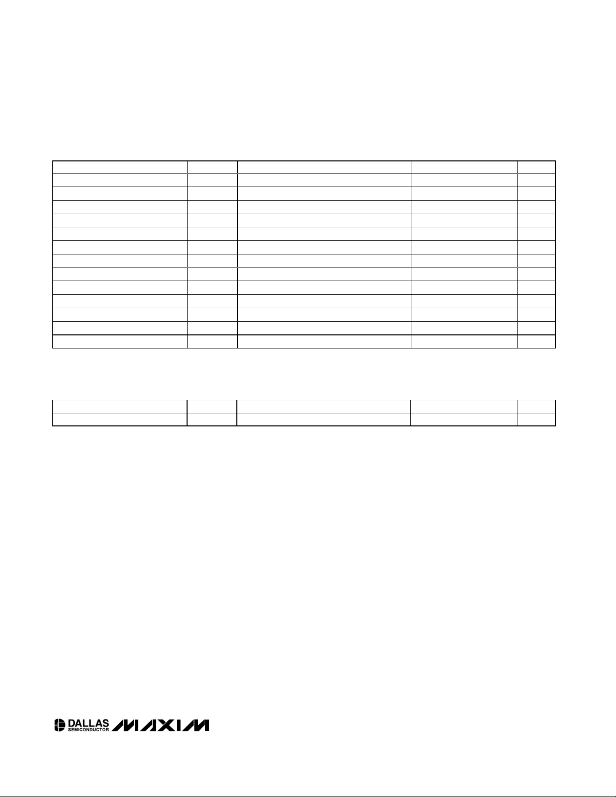
V
CC
GND
CS
INC
U/D
CONTROL
LOGIC UNIT
NONVOLATILE
MEMORY
5-BIT
WIPER
SETTING
POS 31
POS 0
H
L
W
V
CC
Figure 1. Block Diagram
CS
INC
U/D
t
CI
t
IL
t
IH
t
F
t
IC
t
WST
t
CPH
t
DI
t
R
WIPER STORAGE
CONDITION
WIPER NON-STORAGE
CONDITION
WIPER POSITION
POSITION X POSITION X + 1 POSITION X
t
IW
t
IW
t
IK
POSITION X - 1
V
IL
V
IL
V
IL
V
IH
V
IH
t
CLP
Figure 2. Timing Diagram
Page 7

DS4301
Nonvolatile, 32-Position Digital Potentiometer
Maxim cannot assume responsibility for use of any circuitry other than circuitry entirely embodied in a Maxim product. No circuit patent licenses are
implied. Maxim reserves the right to change the circuitry and specifications without notice at any time.
Maxim Integrated Products, 120 San Gabriel Drive, Sunnyvale, CA 94086 408-737-7600 _____________________ 7
© 2003 Maxim Integrated Products Printed USA is a registered trademark of Maxim Integrated Products.
cycled to the device, the wiper setting that was just
stored is the setting loaded on power-up.
Wiper storage does not have to occur immediately after
a change in wiper position. At anytime the current wiper
position can be stored to the EEPROM by simply issuing a low pulse to the CS pin for t
CLP
while the INC pin
remains in a high state. The wiper does not move during this action and the current wiper setting is stored in
EEPROM after t
WST
.
For applications that require a specific wiper setting to
be loaded on power-up and never changed, write the
desired wiper setting to the EEPROM, then tie CS to
VCC. Every time power is cycled to the DS4301, the
desired wiper setting is loaded from EEPROM, and
since CS is tied to VCC, no changes can be made to
the wiper setting.
EEPROM Characteristics
There is a limit to the number of times the EEPROM can
be written to before a wear-out occurs (see the
Nonvolatile Memory Characteristics table). After EEPROM wear-out occurs, the wiper can still be adjusted,
however accurately storing the wiper position is no
longer possible. When power is removed from the part,
the current wiper position is lost. Upon power-up, the
wiper setting stored in EEPROM is loaded within t
WLT
of
V
CC
reaching a stable voltage level greater than or
equal to V
CC MIN
. If EEPROM wear-out has occurred,
the wiper setting that is loaded is unknown.
Application Information
To achieve the best results when using the DS4301,
decouple the power supply with a 0.01µF or 0.1µF
capacitor. Use a high-quality ceramic surface-mount
capacitor when possible. Surface-mount components
minimize lead inductance, improving performace.
Ceramic capacitors tend to have adequate highfrequency response for decoupling applications.
Chip Information
TRANSISTOR COUNT: 3512
SUBSTRATE INFO: P-substrate
Package Information
For the latest package outline information, go to
www.maxim-ic.com/DallasPackInfo
.
 Loading...