Page 1

General Description
The DS4077 is an integrated voltage-controlled crystal
oscillator (VCXO) module designed to provide reference
clock generation in base stations, telecom/datacom, and
wireless applications. The DS4077 is developed using a
fundamental quartz crystal plus a unique integrated circuit design. The internal fundamental quartz crystal
determines the frequency of operation. Custom frequencies are available. Contact the factory for availability.
The DS4077 is designed for use with applications requiring low phase noise and jitter. Jitter performance of better than 0.8ps RMS is achieved over the 12kHz to 20MHz
range. Phase noise performance of better than
-125dBc/Hz at 1kHz is achieved with this design.
Features
♦ 50MHz to 122.88MHz Frequency
♦ 3.135V to 3.465V Operation
♦ Low Jitter: < 0.8ps RMS
♦ ±69ppm Absolute Pull Range (APR)
♦ Output Options:
LVCMOS Output Buffer
LVDS Complementary Output Buffer
♦ Minimum ±110ppm Tuning Range (+25°C)
♦ 14mm x 9mm x 3.06mm Plastic LGA Package
DS4077
50MHz to 122.88MHz VCXO
______________________________________________
Maxim Integrated Products
1
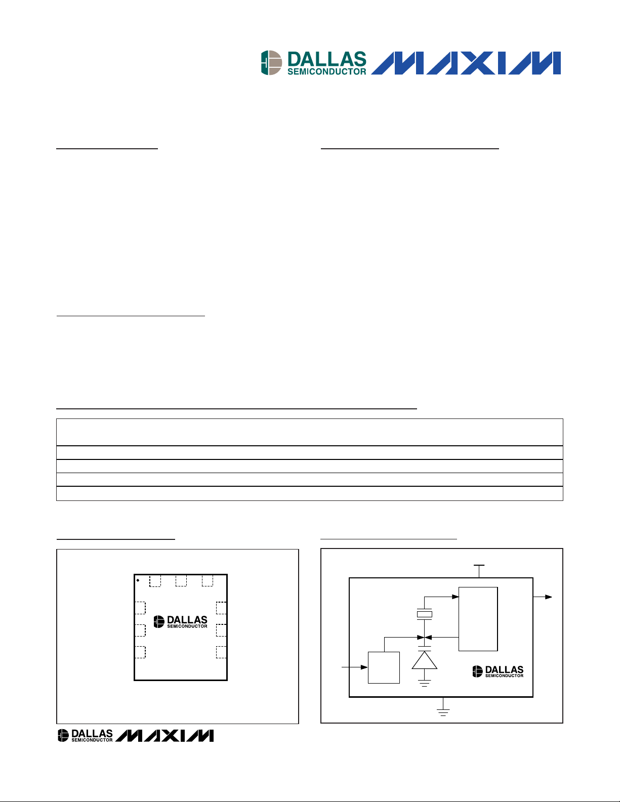
Pin Configuration
Applications
Rev 3; 9/06
For pricing, delivery, and ordering information, please contact Maxim Direct at 1-888-629-4642,
or visit Maxim’s website at www.maxim-ic.com.
Ordering Information
Ordering Information continued at end of data sheet.
Clock-Data Recovery in Telecom/Datacom
Applications
Data Retiming
Reference Clock Generation in Base Stations
and Wireless Applications
Block Diagram
X1
V
DD
LVCMOS
OUTPUT
VARACTOR
OSC
CONTROL
LVCMOS OPTION SHOWN HERE.
CRYSTAL
VC
X2
DS4077
PART TEMP RANGE OUTPUT TYPE
DS4077L-DCN -40°C to +85°C
DS4077L-DDN -40°C to +85°C
DS4077L-CCN -40°C to +85°C
DS4077L-CDN -40°C to +85°C
LVCMOS 54
LVDS 54
LVCMOS 61.44
LVDS 61.44
FREQUENCY
) (MHz)
(f
NOM
PIN-PACKAGE TOP MARK
9 LGA DS4077L-DCN
9 LGA DS4077L-DDN
9 LGA DS4077L-CCN
9 LGA DS4077L-CDN
TOP VIEW
N.C.
( ) LVDS OPTION
TRANSFER-MOLDED PLASTIC PACKAGE
N.C.
9
VC
1
2
34
SS
N.C. N.C.
7
8
6V
DD
DS4077
LGA
5 N.C. (LVDSO-)
LVCMOS (LVDSO+)V
Page 2

DS4077
50MHz to 122.88MHz VCXO
2 _____________________________________________________________________
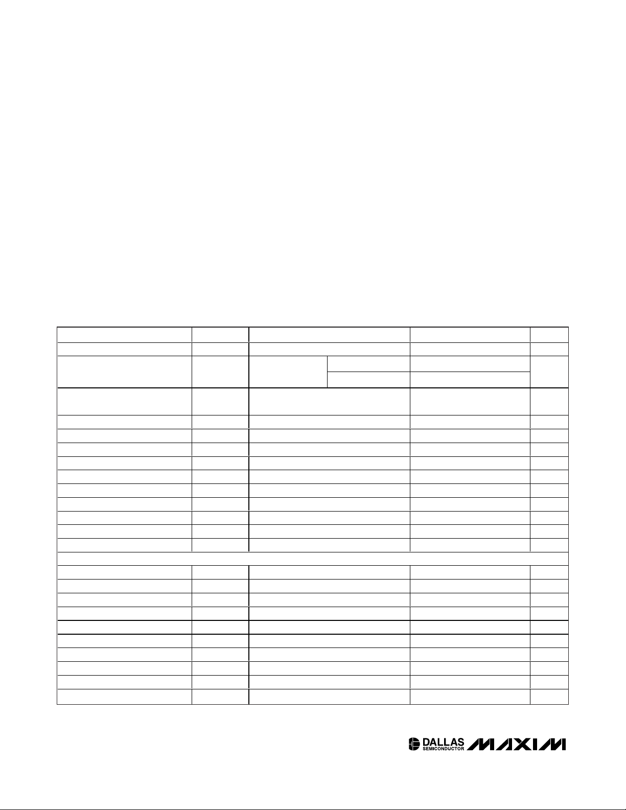
ABSOLUTE MAXIMUM RATINGS
ELECTRICAL CHARACTERISTICS
(VDD= 3.135V to 3.465V, TA= -40°C to +85°C, unless otherwise noted.) (Typical values at +25°C, VDD= 3.3V, unless otherwise
noted.) (Note 1)
Stresses beyond those listed under “Absolute Maximum Ratings” may cause permanent damage to the device. These are stress ratings only, and functional
operation of the device at these or any other conditions beyond those indicated in the operational sections of the specifications is not implied. Exposure to
absolute maximum rating conditions for extended periods may affect device reliability.
VC, VDD, LVCMOS, LVDSO+, LVDSO- Output ........-0.3V, +3.6V
Operating Temperature Range
(noncondensing) ..............................................-40°C to +85°C
Junction Temperature......................................................+150°C
Thermal Resistance
Junction to Ambient .................................................91.06°C/W
Junction to Case ......................................................44.51°C/W
Storage Temperature Range .............................-55°C to +125°C
Soldering Temperature
(reflow, 2 passes max)....See IPC/JEDEC STD-020 Specification
PARAMETER SYMBOL CONDITIONS MIN TYP MAX UNITS
VDD Operating Supply Range V
VDD Supply Current I
Frequency f
Frequency vs. VDD Sensitivity VDDppm VDD = 3.3V ±5% -3.5 +11.5 ppm
Frequency vs. Load Sensitivity LOADpmm 10pF to 20pF (Note 3) -1 ppm/pF
Frequency vs. Temperature TEMPppm From +25°C -20 +20 ppm
VC Voltage Range VC
Frequency Tuning Sensitivity VC
Tuning Voltage Bandwidth VC
Absolute Pull Range f
VC Input Leakage I
Aging, First Year AGEppm -5 +5 ppm
Aging, Years 0–10 t
LVDS OUTPUT
Output High Voltage V
Output Low Voltage V
Differential Output Voltage V
Output Common-Mode Variation V
Offset Output Voltage V
Differential Output Impedeance R
Output Current I
Output Current I
Output Rise Time (Differential) t
Output Fall Time (Differential) t
DD
DD
OUT
RANGE
SEN
BW
TUNE
LCV
AGE
OHLVDSO
OLLVDSO
ODLVDSO
LVDSOCOM
OFFLVDSO
OLVDSO
VSSLVDSO
LVDSO
RLVDSO
FLVDSO
Output open
VC = 1.6V, VDD = 3.3V, TA = +25°C
(Note 2)
(Note 3) 10 kHz
VC = 0.3V to 2.8V (Note 2) -69 +69 ppm
VC = 0V to V
Total aging -10 +10 ppm
(Note 4) 1.475 V
(Note 4) 0.925 V
(Note 4) 250 400 mV
(Note 4) 150 mV
(Note 4) 1.125 1.275 V
(Note 3) 80 140 Ω
Short ground 40 mA
Short together (Note 3) 12 mA
20% to 80% (Note 3) 150 ps
80% to 20% (Note 3) 150 ps
3.135 3.3 3.465 V
f
≤ 106.25MHz 20 30
OUT
f
> 106.25MHz 25 35
OUT
f
NOM
–8ppm
f
NOM
f
NOM
+8ppm
0.3 1.60 2.8 V
41 164 ppm/V
DD
-500 +500 nA
mA
MHz
Page 3

DS4077
50MHz to 122.88MHz VCXO
_____________________________________________________________________ 3
ELECTRICAL CHARACTERISTICS (continued)
(VDD= 3.135V to 3.465V, TA= -40°C to +85°C, unless otherwise noted.) (Typical values at +25°C, VDD= 3.3V, unless otherwise
noted.) (Note 1)
Note 1: Limits at -40°C are guaranteed by design and not production tested.
Note 2: 10pF, LVCMOS.
Note 3: Guaranteed by design and not production tested.
Note 4: 100Ω differential load.
Pin Description
PIN
LVCMOS
LVDS
NAME FUNCTION
1
1
VC VCXO Control Voltage
2, 5, 7, 8, 9
2, 7, 8, 9
N.C. No Connection
3
3
V
SS
Ground
4
—
LVCMOS LVCMOS Output
6
6
V
DD
DC Power
—
4, 5
LVDSO+/LVDSO- LVDS Positive and Negative Outputs
LVCMOS OUTPUT
Output Logic 0 V
Output Logic 1 V
Output Rise Time t
Output Fall Time t
Duty Cycle D
Harmonics H VDD = 3.3V, TA = +25°C (Note 3) -18 -8 dBc/Hz
SSB PHASE NOISE AND JITTER, VDD = 3.3, TA = +25°C (Note 3)
10Hz Offset -70
100Hz Offset -100
1kHz Offset -125
10kHz Offset -145
100kHz Offset
Jitter (12kHz to 20MHz) 0.8 ps
PARAMETER SYMBOL CONDITIONS MIN TYP MAX UNITS
OL
OH
R
F
CYC
Output Current -450µA 0 0.4 V
-
V
Output Current +450µA
Load condition: 10pF to ground; 10% to
90% V
Load condition: 10pF to ground; 90% to
10% V
Load condition: 10pF, V
LVCMOS
(Note 3)
DD
(Note 3)
DD
/ 2 (Note 3) 40 60 %
DD
DD
0.8V
-150
V
DD
2ns
2ns
dBc/Hz
V
RMS
Page 4

DS4077
50MHz to 122.88MHz VCXO
4 _____________________________________________________________________
Typical Operating Characteristics
(VCC= +3.3V, TA= +25°C, unless otherwise noted.)
FREQUENCY vs. TEMPERATURE
DS4077 toc01
TEMPERATURE (°C)
f
OUT
DEVIATION (ppm)
60
40
20
0
-20
-8
-6
-4
-2
0
2
4
6
8
10
-10
-40
80
f
OUT
= 77.76MHz
VC = 1.55V
LVCMOS OUTPUT FREQUENCY
vs. LOAD CAPACITANCE vs. VC
DS4077 toc02
VC (V)
f
OUT
DEVIATION (ppm)
2.8
1.8
2.3
1.30.8
-50
-75
-100
125
100
75
50
25
0
-25
150
-125
0.3
CL = 0pF
CL = 20pF
f
OUT
= 77.76MHz
OUTPUT FREQUENCY
vs. SUPPLY VOLTAGE vs. VC
DS4077 toc03
VDD (V)
f
OUT
DEVIATION FROM V
DD
= 3.3V (ppm)
3.410 3.465
3.3553.190 3.245
3.300
-10
-15
15
10
5
0
-5
20
-20
3.135
f
OUT
= 77.76MHz
T
A
= +25°C
VC = 0.3V
VC = 2.8V
VC = 1.6V
Page 5

DS4077
50MHz to 122.88MHz VCXO
Maxim cannot assume responsibility for use of any circuitry other than circuitry entirely embodied in a Maxim product. No circuit patent licenses are
implied. Maxim reserves the right to change the circuitry and specifications without notice at any time.
Maxim Integrated Products, 120 San Gabriel Drive, Sunnyvale, CA 94086 408-737-7600 _____________________
5
© 2006 Maxim Integrated Products Maxim is a registered trademark of Maxim Integrated Products, Inc.
is a registered trademark of Dallas Semiconductor Corporation.
Ordering Information (continued)
Revision History
Rev 0; 8/05: Initial release.
Rev 1; 12/05: Added LVDS option.
Rev 2; 6/06: Changed device description/frequency range; changed jitter typical value from 1 to 0.8psRMS;
added new parts numbers to Ordering Information table; changed jitter range upper limits from
80MHz to 20MHz.
Rev 3; 9/06: Changed V
DD
ppm units from ppm/PF to ppm; added separate IDDparameter for parts with f
OUT
greater than 106.25MHz.
PACKAGE TYPE PACKAGE CODE DOCUMENT NO.
9 LGA L949A-1
21-0265
Package Information
For the latest package outline information and land patterns, go to www.maxim-ic.com/packages.
PART TEMP RANGE OUTPUT TYPE
DS4077L-ECN -40°C to +85°C
DS4077L-EDN -40°C to +85°C
DS4077L-FCN -40°C to +85°C
DS4077L-FDN -40°C to +85°C
DS4077L-ACN -40°C to +85°C
DS4077L-ADN -40°C to +85°C
DS4077L-0CN -40°C to +85°C
DS4077L-0DN -40°C to +85°C
DS4077L-GCN -40°C to +85°C
DS4077L-GDN -40°C to +85°C
DS4077L-BDN -40°C to +85°C
FREQUENCY
) (MHz)
(f
NOM
LVCMOS 74.17582
LVDS 74.17582
LVCMOS 74.25
LVDS 74.25
LVCMOS 76.8
LVDS 76.8
LVCMOS 77.76
LVDS 77.76
LVCMOS 106.25
LVDS 106.25
LVDS 122.88
PIN-PACKAGE TOP MARK
9 LGA DS4077L-ECN
9 LGA DS4077L-EDN
9 LGA DS4077L-FCN
9 LGA DS4077L-FDN
9 LGA DS4077L-ACN
9 LGA DS4077L-ADN
9 LGA DS4077L-0CN
9 LGA DS4077L-0DN
9 LGA DS4077L-GCN
9 LGA DS4077L-GDN
9 LGA DS4077L-BDN
 Loading...