

Page 1
General Description
The DS4026 is a temperature-compensated crystal
oscillator (TCXO) that provides ±1ppm frequency stability over the -40°C to +85°C industrial temperature range.
The DS4026 is also available in Stratum 3 versions (see
the
Ordering Information—Stratum 3
table). Each device
is factory calibrated over temperature to achieve the
±1ppm frequency stability. Standard frequencies for the
device include 10, 12.8, 19.44, 20, 38.88, 40, and
51.84MHz. Contact the factory for custom frequencies.
The DS4026 provides excellent phase-noise characteristics. The output is a push-pull CMOS square wave with
symmetrical rise and fall times. In addition, the DS4026
is designed to provide a maximum frequency deviation
of less than ±4.6ppm over 20 years. The device also
provides an I2C interface to allow pushing and pulling
of the output frequency by a minimum of ±8ppm
(±5ppm for 10MHz) with typical 1ppb resolution.
The DS4026 implements a temperature-to-voltage conversion with a nonlinear relationship. The output from
the temperature-to-voltage converter is used to drive
the voltage-controlled crystal oscillator to compensate
for frequency change.
The device implements an on-chip temperature sensor
lookup table, and a digital-to-analog converter (DAC) to
adjust the frequency. An I
2
C interface used to communicate with the DS4026 performs temperature readings
and frequency push-pull.
Applications
Reference Clock Generation Wireless
Telecom/Datacom/SATCOM Test and Measurement
Features
♦ ±1ppm Frequency Accuracy Over -40°C to +85°C
♦ Standard Frequencies: 10, 12.8, 19.44, 20, 38.88,
40, 51.84MHz
♦ Stratum 3 Frequencies: 10, 12.8, 19.2, 20MHz
♦ Maximum ±4.6ppm Deviation Over 20 Years
♦ Minimum ±8ppm (±5ppm for 10MHz) Digital
Frequency Tuning Through I
2
C Interface
♦ Surface-Mount 16-Pin SO Package
♦ Pb Free/RoHS Compliant
DS4026
10MHz to 51.84MHz TCXO
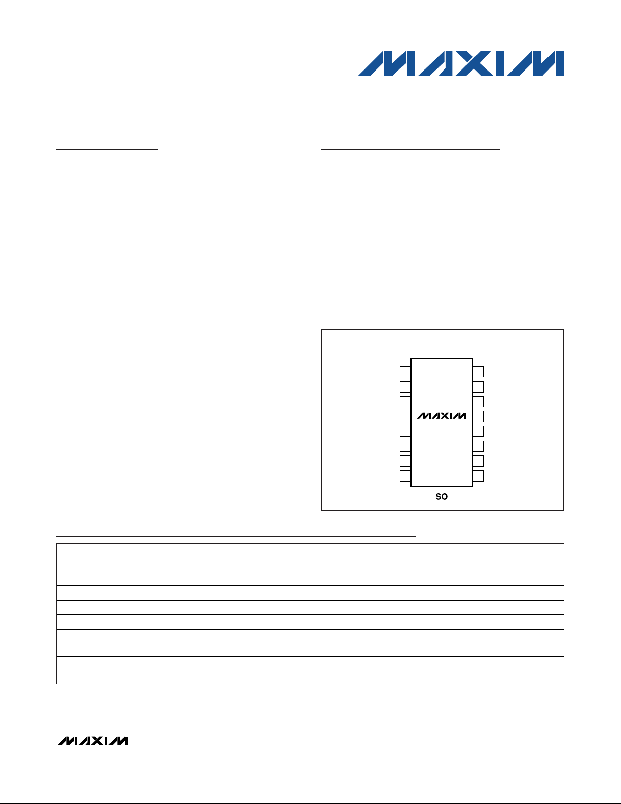
Pin Configuration
Rev 2; 4/08
________________________________________________________________
Maxim Integrated Products
1
For pricing, delivery, and ordering information, please contact Maxim Direct at 1-888-629-4642,
or visit Maxim’s website at www.maxim-ic.com.
+
Denotes a lead(Pb)-free/RoHS-compliant package.
*The top mark will include a “+” for a lead(Pb)-free/RoHS-compliant device.
Ordering Information continued at end of data sheet.
Ordering Information
TOP VIEW
V
V
OSC
N.C.
N.C.
N.C.
REF
+
1
2
3
CC
4
DS4026
5
6
7
8
16
V
CCD
FOUT
15
GNDD
14
SCL
13
SDA
12
GND
11
N.C.
10
N.C.
9
GNDA
V
GNDOSC
PART TEMP RANGE
DS4026S+ACC
DS4026S+ACN
DS4026S+BCC
DS4026S+BCN -40°C to +85°C 12.80 16 SO DS4026-BCN
DS4026S+ECC 0°C to +70°C 16.80 16 SO DS4026-ECC
DS4026S+ECN -40°C to +85°C 16.80 16 SO DS4026-ECN
DS4026S+FCC 0°C to +70°C 16.384 16 SO DS4026-FCC
DS4026S+FCN -40°C to +85°C 16.384 16 SO DS4026-FCN
0°C to +70°C 10.00 16 SO DS4026-ACC
-40°C to +85°C 10.00 16 SO DS4026-ACN
0°C to +70°C 12.80 16 SO DS4026-BCC
OUTPUT (f
(MHz, CMOS)
)
C
PIN-PACKAGE TOP MARK*
Page 2
DS4026
10MHz to 51.84MHz TCXO
2 _______________________________________________________________________________________
ABSOLUTE MAXIMUM RATINGS
RECOMMENDED DC OPERATING CONDITIONS
(TA= -40°C to +85°C, unless otherwise noted.)
Stresses beyond those listed under “Absolute Maximum Ratings” may cause permanent damage to the device. These are stress ratings only, and functional
operation of the device at these or any other conditions beyond those indicated in the operational sections of the specifications is not implied. Exposure to
absolute maximum rating conditions for extended periods may affect device reliability.
Voltage Range on V
CC
,
V
CCD
, and V
OSC
Relative to Ground..............................................-0.3V to +3.8V
Voltage Range on SDA, SCL, and FOUT
Relative to Ground...................................-0.3V to (V
CC
+ 0.3V)
Operating Temperature Range (noncondensing)....-40°C to +85°C
Storage Temperature Range ...............................-40°C to +85°C
Soldering Temperature...........................Refer to the IPC/JEDEC
J-STD-020 Specification.
DC ELECTRICAL CHARACTERISTICS
(VCC= 3.135V to 3.465V, TA= -40°C to +85°C, unless otherwise noted.) (Notes 1, 2, 3)
Power-Supply Voltage VCC 3.135 3.3 3.465 V
Oscillator Power Supply V
Driver Power Supply V
PARAMETER SYMBOL CONDITIONS MIN TYP MAX UNITS
OSC
CCD
VCC Active-Supply Current ICC (Note 4) 1.5 2.5 mA
V
OSC
Current
V
CCD
Current
SCL Input Lea kage ILI -1 +1 μA
SDA Leakage ILO Output off -1 +1 μA
SCL, SDA High Input Voltage V
SCL, SDA Low Input Voltage VIL -0.3
SDA Logic 0 Output IOL VCC = 3.0V, VOL = 0.4V 3 mA
FOUT High Output Voltage VOH V
FOUT Low Output Voltage VOL V
FOUT Rise/Fall Time tR/tF (0.1 x V
FOUT Duty C yc le tD 0.5 x V
PARAMETER SYMBOL CONDITIONS MIN TYP MAX UNITS
FOUT CMOS output on, CL = 10pF,
Oscillator Active-Supply
Driver Active-Supply
I
OSC
I
CCD
frequency < 25MHz
FOUT CMOS output on, CL = 10pF,
frequency 25MH z
FOUT CMOS output on, CL = 10pF,
frequency < 25MHz
FOUT CMOS output on, CL = 10pF,
frequency 25MH z
IH
= 3V, IOH = -2mA 2.4 V
CCD
= 3V, IOL = 2.0mA 0.4 V
CCD
CCD
CCD
3.135 3.3 3.465 V
3.135 3.3 3.465 V
0.7 x
V
CC
) - (0.9 x V
(Note 5) 45 55 %
) 2 ns
CCD
3 4
5 9
2 3
3 5
V
CC
+ 0.3
+0.3 x
V
CC
mA
mA
V
V
Page 3
DS4026
10MHz to 51.84MHz TCXO
_______________________________________________________________________________________ 3
AC ELECTRICAL CHARACTERISTICS—TCXO
(VCC= 3.135V to 3.465V, TA= -40°C to +85°C, unless otherwise noted.) (Note 1)
AC ELECTRICAL CHARACTERISTICS—STRATUM 3
(VCC= +3.135V to +3.465V, TA= -40°C to +85°C, unless otherwise noted.) (Note 1)
PHASE NOISE
Frequency Stability vs.
Temperature
Frequency Stability vs. Voltage
Aging
Frequency Pull
Range
Frequency Pull Re so lution f
PARAMETER SYMBOL CONDITIONS MIN TYP MAX UNITS
f/f
CL = 10pF to ground
C
f
VOLTAGE
/f
First Year -1 +1
Years 2–20
Except 10MHz ±8 ±15
10MHz
f
AGING/fC
f/f
RES/fC
CL = 10pF to ground, +25°C -2 +2 ppm/V
C
(Note 5)
FTUNEH = 3Fh and FTUNEL = FFh;
C
FTUNEH = 40h and FTUNEL = 00h at +25°C
1 ppb
STRATUM 3 FREQUENCY STABILITY
Frequency Stability vs.
Temperature
Initial Tolerance and Reflow f
Frequency Stability vs. Voltage
Frequency Stability vs.
Aging/20 Years
Frequency Stability vs. Load
Change
Free-Run Accuracy
Holdover Stability (24 Hours)
PARAMETER SYMBOL CONDITIONS MIN TYP MAX UNITS
f
INITIAL
f
VOLTAGE
f
AGING/fC fC
f
f
24HOURS
-40°C to +85°C (Note 6) -0.28 +0.28 ppm
TEMP/fC
/fC TA = +25°C, ±3°C and VDD = 3.3V -0.8 +0.8 ppm
VCC = 3.3V ±5%, CL = 10pF to ground,
/f
LOAD/fC
/f
+25°C (Note 7)
C
= Nominal (Note 8) -3.0 +3.0 ppm
Load = 10pF ±5%, +25°C (Note 5) -0.1 +0.1 ppm
Operating temperature, load, supply, and
initial tolerance, aging (20 years) (Notes 5, 8)
24-hour elapsed time (Notes 5, 9) -0.32 +0.32 ppm
C
f
C
– 1ppm
-2 +2
±5 ±10
-0.33 +0.33 ppm
-4.6 +4.6 ppm
f
C
f
C
+ 1ppm
ppm
ppm
ppm
CARRIER
FREQUENCY
PHASE NOISE (dBc/Hz) (TYPICAL, +25°C, 3.3V)
OFFSET (MHz) 10Hz 100Hz 1kHz 10kHz 100kHz 1MHz
12.80 -88.41 -130.16 -147.84 -150.84 -151.71 -151.87
19.44 -82.63 -125.12 -145.03 -146.87 -151.69 -151.52
20.00 -83.71 -120.76 -145.44 -150.96 -151.18 -151.45
38.88 -79.01 -120.06 -141.75 -150.59 -152.50 -153.06
40.00 -80.80 -115.44 -141.17 -151.59 -152.37 -153.00
51.84 -74.09 -120.39 -142.33 -151.14 -153.21 -153.94
10.0 -92.52 -134.83 -147.22 -150.84 -151.25 -150.84
16.384 -87.44 -128.53 -147.67 -150.78 -152.72 -151.75
16.8 -89.6 -126.20 -146.88 -151.90 -152.28 -151.93
24.0 -83.98 -119.45 -143.08 -150.33 -150.34 -150.67
Page 4
AC ELECTRICAL CHARACTERISTICS—I2C SERIAL INTERFACE
(VCC= 3.135V to 3.465V, TA= -40°C to +85°C, unless otherwise noted.) (Note 2)
DS4026
10MHz to 51.84MHz TCXO
4 _______________________________________________________________________________________
TEMPERATURE SENSOR ELECTRICAL CHARACTERISTICS
(VCC= 3.135V to 3.465V, TA= -40°C to +85°C, unless otherwise noted.) (Note 1)
PARAMETER SYMBOL CONDITIONS MIN TYP MAX UNITS
Temperature Sensor Accuracy T -3 +3 °C
Temperature Sensor Conversion
Time
Temperature Sensor Resolution N2 12 Bits
PARAMETER SYMBOL CONDITIONS MIN TYP MAX UNITS
SCL Clock Frequenc y f
Bus Free Time Between STOP
and START Condition s
Hold Time (Repeated) START
Condition (Note 10)
Low Period of SCL Clock t
High Period of SCL Clock t
Data Hold Time
(Notes 11, 12)
Data Setup Time (Note 13) t
START Setup Time t
Rise Time of Both SDA and SCL
Signals (Note 14)
Fal l Time of Both SDA and SCL
Signals (Note 14)
Setup Time for STOP Condition t
Pin Capacitance SDA, SCL
(Note 5)
t
11 ms
CONVT
SCL
t
BUF
t
HD: STA
LOW
HIGH
t
HD:DAT
SU:DAT
SU:STA
t
t
SU:STO
C
I/O
Standard mode 0 100
Fast mode 100 400
Standard mode 4.7
Fast mode 1.3
Standard mode 4.0
Fast mode 0.6
Standard mode 4.7
Fast mode 1.3
Standard mode 4.0
Fast mode 0.6
Standard mode 0 0.9
Fast mode 0 0.9
Standard mode 250
Fast mode 100
Standard mode 4.7
Fast mode 0.6
Standard mode 20 + 0.1CB 1000
R
Fast mode 20 + 0.1CB 300
Standard mode 20 + 0.1CB 300
F
Fast mode 20 + 0.1CB 300
Standard mode 4.7
Fast mode 0.6
10 pF
kHz
μs
μs
μs
μs
μs
ns
μs
ns
ns
μs
Page 5
DS4026
Note 1: Typical values are at +25°C, nominal supply voltages, unless otherwise indicated.
Note 2: Voltages referenced to ground.
Note 3: Limits at -40°C are guaranteed by design and not production tested.
Note 4: Specified with I
2
C bus inactive.
Note 5: Guaranteed by design and not production tested.
Note 6: Frequency stability vs. temperature is defined as (Δf
MAX
- Δf
MIN
)/2.
Note 7: Maximum power-supply variations to meet the specification are 5%.
Note 8: Crystal vendor specification.
Note 9: Holdover is defined as (f
MAX
- f
MIN
)/2 as measured within a 24-hour period. Warmup time = 1 hour.
Note 10: After this period, the first clock pulse is generated.
Note 11: A device must internally provide a hold time of at least 300ns for the SDA signal (referred to the V
IH(MIN)
of the SCL signal)
to bridge the undefined region of the falling edge of SCL.
Note 12: The maximum t
HD:DAT
need only be met if the device does not stretch the low period (t
LOW
) of the SCL signal.
Note 13: A fast-mode device can be used in a standard-mode system, but the requirement that t
SU:DAT
≥ 250ns must then be met.
This is automatically the case if the device does not stretch the low period of the SCL signal. If such a device does not
stretch the low period of the SCL signal, it must output the next data bit to the SDA line t
R(MAX)
+ t
SU:DAT
= 1000 + 250 =
1250ns before the SCL line is released.
Note 14: C
B
—total capacitance of one bus line in pF.
AC ELECTRICAL CHARACTERISTICS—I2C SERIAL INTERFACE (continued)
(VCC= 3.135V to 3.465V, TA= -40°C to +85°C, unless otherwise noted.) (Note 2)
10MHz to 51.84MHz TCXO
_______________________________________________________________________________________ 5
Data Transfer on I2C Serial Bus
PARAMETER SYMBOL CONDITIONS MIN TYP MAX UNITS
Capacitive Load for Each Bus
Line (Note 14)
Pulse Width of Spikes That Must
Be Suppressed by the Input
Filter
400 pF
C
B
t
Fast mode 30 ns
SP
SDA
SCL
t
BUF
STOP START
t
t
t
SU:STA
HD:STA
t
LOW
t
HD:STA
t
R
t
HD:DAT
t
F
t
HIGH
t
SU:DAT
REPEATED
START
SP
t
SU:STO
Page 6

DS4026
10MHz to 51.84MHz TCXO
6 _______________________________________________________________________________________
Typical Operating Characteristics
(VCC= +3.3V, TA = +25°C, unless otherwise noted.)
ACTIVE-SUPPLY CURRENT
vs. POWER-SUPPLY CURRENT
DS4026 toc01
VCC (V)
CURRENT (mA)
3.53.43.33.23.1
0.3
0.2
0.1
0.6
0.5
0.4
0.8
0.7
0.9
1.1
1.0
1.4
1.3
1.2
1.6
1.5
0
3.0 3.6
12.8
51.84
ACTIVE-SUPPLY CURRENT
vs. OSCILLATOR POWER SUPPLY
DS4026 toc02
V
OSC
(V)
CURRENT (mA)
3.53.43.33.23.1
0.5
1.0
1.5
2.0
2.5
3.0
3.5
4.0
4.5
5.0
0
3.0 3.6
51.84
12.8
ACTIVE-SUPPLY CURRENT
vs. DRIVER POWER SUPPLY
DS4026 toc03
V
CCD
(V)
CURRENT (mA)
3.53.43.33.23.1
8.0
6.0
4.0
2.0
10.0
-0.1
3.0 3.6
51.84
12.8
FREQUENCY vs. FTUNE
DS4026 toc04
VC (V)
OFFSET (ppm)
000h4000h
-25
-20
-15
-10
-5
0
5
10
15
20
-30
3FFFh
12.8
51.84
FREQUENCY vs. TEMPERATURE
DS4026 toc05
TEMPERATURE (°C)
DEVIATION (ppm)
6040
200
-20
-10
-13
-8
-3
-5
3
15
13
10
8
5
18
0
20
-15
-40
80
DCOMP = 1
DCOMP = 0
PHASE NOISE (TYP)
DS4026 toc06
OFFSET (Hz)
PHASE NOISE (dBc/Hz)
-5.0
-30.0
-55.0
-80.0
-105.0
-130.0
-155.0
-180.0
10 100 1000 10,000 100,000 1,000,000
51.84MHz
12.8MHz
19.44MHz
38.88MHz
Page 7

DS4026
10MHz to 51.84MHz TCXO
_______________________________________________________________________________________ 7
Pin Description
PIN NAME FUNCTION
1 GNDA Ground for DAC
2 V
REF
Voltage Reference Output. Thi s pin must be decoupled with a 100μF ceramic capac itor to ground.
3 V
CC
Power Supply for Digital Control and Temperature Sensor. This pin must be decoupled with a
100nF capacitor to ground.
4 V
OSC
Power Supply for Oscillator Circuit. This pin must be decoupled with a 0.1μF capacitor to ground.
5 GNDOSC Ground for Oscillator Circuit
6–10 N.C. No Connection. Must be connected to ground.
11 GND Ground for Digital Control, Temperature Sensor, and Controller Substrate
12 SDA
Serial Data Input/Output. SDA is the data input/output for the I
2
C interface. This open-drain pin
requires an external pullup resistor.
13 SCL
Serial Clock Input. SCL is the cloc k input for the I
2
C Interface and i s u sed to synchronize data
movement on the serial interface.
14 GNDD Ground for Oscillator Output Driver
15 FOUT Frequency Output, CMOS Push-Pull
16 V
CCD
Power Supply for Oscillator Output Driver. This pin must be decoupled with a 0.1μF capacitor to
ground. A 20 resistor must be placed in series between the power supply and V
CCD
.
Figure 1. Typical Operating Circuit
100μF ±20%
CERAMIC
GNDA
V
REF
V
CCD
FOUT
GNDD
DS4026
V
CC
3.3V
0.1μF
0.1μF
3.3V
V
OSC
GNDOSC
N.C.
N.C.
N.C.
SCL
SDA
GND
N.C.
N.C.
0.1μF
20Ω
3.3V ±5%
Page 8

DS4026
10MHz to 51.84MHz TCXO
8 _______________________________________________________________________________________
Figure 2. Functional Diagram
Detailed Description
The DS4026 is a TCXO capable of operating at 3.3V
±5%, and it allows digital tuning of the fundamental frequency. The device is calibrated in the factory to
achieve an accuracy of ±1ppm over the industrial temperature range, and its minimum pullability is ±8ppm
with a typical resolution of 1ppb (typ) per LSB.
The DS4026 contains the following blocks:
• Oscillator block with variable capacitor for compensation
• Output driver block
• Temperature sensor
• Controller to read the temperature, control lookup
table, and adjust the DAC input
• DAC output to adjust the capacitive load
•I
2
C interface to communicate with the chip
The oscillator block consists of an amplifier and variable
capacitor in a Pierce crystal oscillator with a crystal resonator of fundamental mode. The oscillator amplifier is a
single transistor amplifier and its transconductance is
temperature compensated. The variable capacitor is
adjusted by the DAC to provide temperature compensation. With the FTUNEH and FTUNEL registers, a minimum
pullability of ±8ppm (±5ppm for 10MHz) is achieved with
a typical resolution of 1ppb (typ) per LSB.
V
CC
V
CC
GND
SCL
SDA
V
OSC
V
CC
2
C
I
INTERFACE
GND
TEMP
SENSOR
V
CC
CONTROLLER
GND
A/D
GND
DAC
EEPROM
ARRAY
DS4026
CMOS
BUFFER
V
REF
GNDA
V
CCD
FOUT
GNDOSC GNDD
Page 9

DS4026
10MHz to 51.84MHz TCXO
_______________________________________________________________________________________ 9
The output driver is a CMOS square-wave output with
symmetrical rise and fall time.
The temperature sensor provides a 12-bit temperature
reading with a resolution of 0.0625°C. The sensor is in
continuous conversion mode. If DCOMP is set, conversions continue but temperature updates are inhibited.
The controller coordinates the conversion of temperature into digital codes. When the temperature reading is
different from the previous one or the frequency tuning
register is changed, the controller looks up the two corresponding capacitance trim codes from the lookup
table at a 0.5°C increment. The trim codes are interpolated to 0.0625°C resolution.
The result is added with the tuning value from the frequency tuning register and loaded into the DAC registers to adjust voltage output. The monotonic DAC
provides an analog voltage based on temperature
compensation to drive the variable capacitor.
The DS4026 operates as a slave device on the serial
bus. Access is obtained by implementing a START
condition and providing a device identification code followed by data. Subsequent registers can be accessed
sequentially until a STOP condition is executed.
Address Map
Disable Compensation Update (DCOMP)
DCOMP is bit 7 of the frequency tuning register (see
the
Frequency Tuning Register (00h–01h), POR = 00h
table). When set to logic 1, this bit’s temperature-compensation function is disabled. This disabling prevents
the variable capacitor in the oscillator block from
changing. However, the temperature register still performs temperature conversions. The temperature trim
code from the last temperature conversion before
DCOMP is enabled is used for temperature compensation. The FTUNE registers are still functional when
DCOMP is disabled.
The frequency tuning registers adjust the base frequency. The frequency tuning value is represented in two’s
complement data. Bit 6 of FTUNEH is the sign, bit 5 is
the MSB, and bit 0 of FTUNEL is the LSB (see Table 1).
When the tuning register low (01h) is programmed with
a value, the next temperature update cycle sums the
programmed value with the factory compensated
value. This allows the user to digitally control the base
frequency using the I
2
C protocol.
These frequency tuning register bits allow the tuning of
the base frequency. Each bit typically represents
about 1ppb (typ). For FTUNEH = 3Fh and FTUNEL =
FFh, the device pushes the base frequency by approximately +15ppm.
Frequency Tuning Register (00h–01h), POR = 00h
Temperature Register (02h–03h)
ADDRESS BIT 7 BIT 6 BIT 5 BIT 4 BIT 3 BIT 2 BIT 1 BIT 0
00h DCOMP Sign Data Data Data Data Data Data
POR 0 0 0 0 0 0 0 0
01h Data Data Data Data Data Data Data Data
POR 0 0 0 0 0 0 0 0
ADDRESS BIT 7 BIT 6 BIT 5 BIT 4 BIT 3 BIT 2 BIT 1 BIT 0
02h Sign Data Data Data Data Data Data Data
POR 0 0 0 0 0 0 0 0
03h Data Data Data Data 0 0 0 0
POR 0 0 0 0 0 0 0 0
Page 10

DS4026
10MHz to 51.84MHz TCXO
10 ______________________________________________________________________________________
Read Mode
In the temperature register (see the
Temperature
Register (02h–03h)
table), temperature is represented
as a 12-bit code and is accessible at location 02h and
03h. The upper 8 bits are at location 02h and the lower
4 bits are in the upper nibble of the byte at location
03h. Upon power reset, the registers are set to a +25°C
default temperature and the controller starts a temperature conversion. The temperature register stores new
temperature readings.
The current temperature is loaded into the (user) temperature registers when a valid I2C slave address and
write is received and when a word address is received.
Consequently, if the two temperature registers are read
in individual I2C transactions, it is possible for a temperature conversion to occur between reads, and the
results can be inaccurate. To prevent this from occurring, the registers should be read using a single, multibyte read operation (Figure 5). I2C reads do not affect
the internal temperature registers.
I
2
C Serial Data Bus
The DS4026 supports a bidirectional I2C bus and data
transmission protocol. A device that sends data onto
the bus is defined as a transmitter and a device receiving data is defined as a receiver. The device that controls the message is called a master. The devices that
are controlled by the master are slaves. The bus must
be controlled by a master device that generates the
serial clock (SCL), controls the bus access, and generates the START and STOP conditions. The DS4026
operates as a slave on the I2C bus. Connections to the
bus are made through the open-drain I/O lines SDA
and SCL. Within the bus specifications, a standard
mode (100kHz maximum clock rate) and a fast mode
(400kHz maximum clock rate) are defined. The DS4026
works in both modes.
The following bus protocol has been defined (Figure 3):
• Data transfer can be initiated only when the bus is
not busy.
Table 1. Register Map
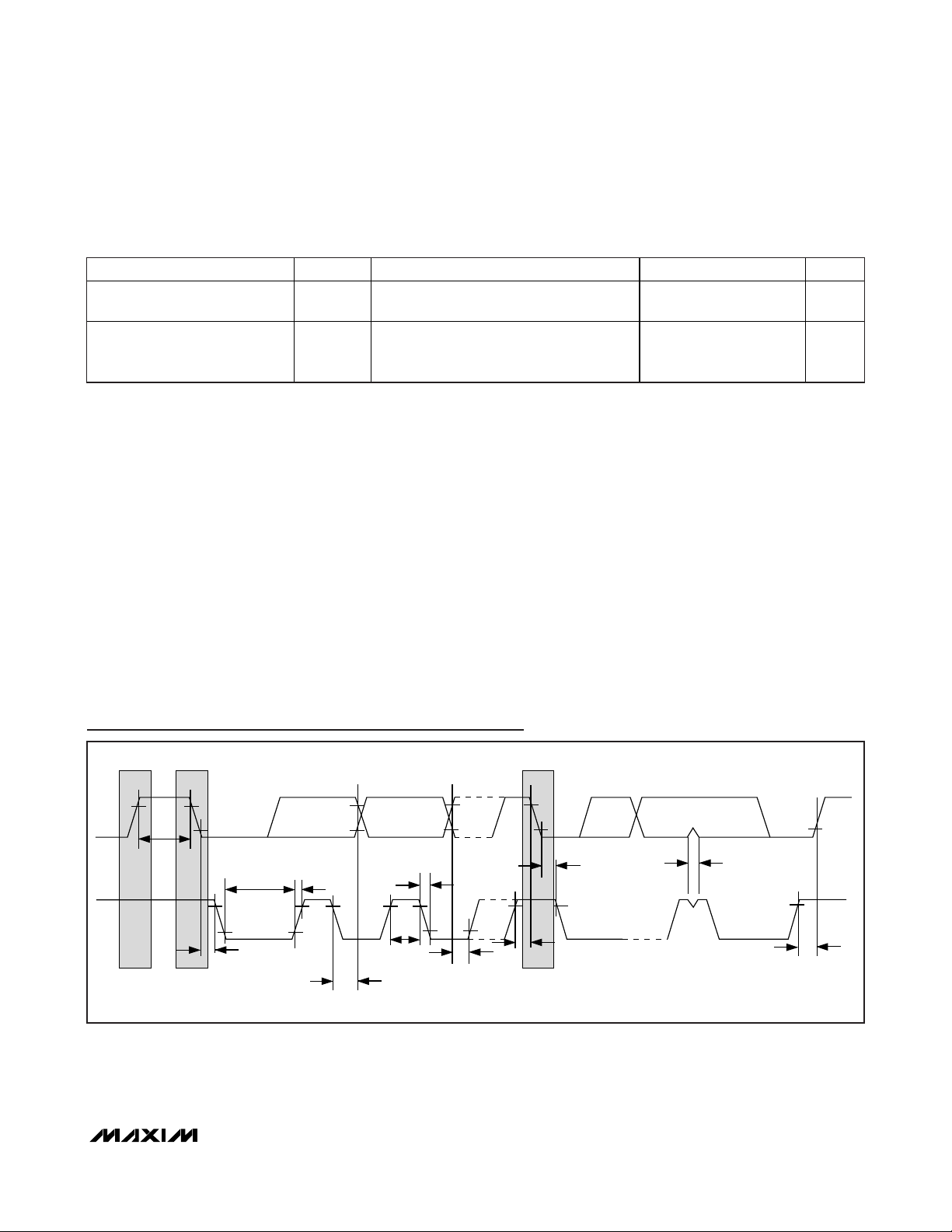
Figure 3. I2C Data Transfer Overview
ADDRESS BIT 7 BIT 6 BIT 5 BIT 4 BIT 3 BIT 2 BIT 1 BIT 0 FUNCTION
00 DCOMP SIGN FTUNEH Frequency Tuning High
01 FTUNEL Frequency Tuning Low
02 SIGN TREGH Temperature MSB
03 TREGL Temperature LSB
SDA
MSB
SLAVE ADDRESS
SCL
12 678 9 12 893–7
START
CONDITION
R/W
DIRECTION
BIT
ACKNOWLEDGEMENT
SIGNAL FROM RECEIVER
ACK
ACKNOWLEDGEMENT
SIGNAL FROM RECEIVER
REPEATED IF MORE BYTES
ARE TRANSFERED
ACK
STOP
CONDITION
OR REPEATED
START
CONDITION
Page 11

DS4026
10MHz to 51.84MHz TCXO
______________________________________________________________________________________ 11
• During data transfer, the data line must remain stable
whenever the clock line is high. Changes in the data
line while the clock line is high are interpreted as
control signals.
Accordingly, the following bus conditions have been
defined:
Bus not busy: Both data and clock lines remain
high.
START data transfer: A change in the state of the
data line from high to low, while the clock line is high,
defines a START condition.
STOP data transfer: A change in the state of the
data line from low to high, while the clock line is high,
defines a STOP condition.
Data valid: The state of the data line represents valid
data when, after a START condition, the data line is
stable for the duration of the high period of the clock
signal. The data on the line must be changed during
the low period of the clock signal. There is one clock
pulse per bit of data.
Each data transfer is initiated with a START condition
and terminated with a STOP condition. The number
of data bytes transferred between the START and the
STOP conditions is not limited, and is determined by
the master device. The information is transferred
byte-wise and each receiver acknowledges with a
ninth bit.
Acknowledge: Each receiving device, when
addressed, is obliged to generate an acknowledge
(ACK) after the reception of each byte. The master
device must generate an extra clock pulse that is
associated with this acknowledge bit.
A device that acknowledges must pull down the SDA
line during the acknowledge clock pulse in such a
way that the SDA line is stable low during the high
period of the acknowledge-related clock pulse. Of
course, setup and hold times must be taken into
account. A master must signal an end of data to the
slave by not generating an acknowledge bit on the
last byte that has been clocked out of the slave. In
this case, the slave must leave the data line high to
enable the master to generate the STOP condition.
Figures 4 and 5 detail how data transfer is accomplished on the I2C bus. Depending upon the state of
the R/W bit, two types of data transfer are possible:
Data transfer from a master transmitter to a slave
receiver. The first byte transmitted by the master is
the slave address. Next follows a number of data
bytes. The slave returns an acknowledge (ACK) bit
after each received byte.
Data transfer from a slave transmitter to a master
receiver. The first byte (the slave address) is trans-
mitted by the master. The slave then returns an
acknowledge bit. Next follows a number of data
bytes transmitted by the slave to the master. The
master returns an acknowledge bit after all received
bytes other than the last byte. At the end of the last
received byte, a not acknowledge (NACK) is
returned.
The master device generates all the serial clock
pulses and the START and STOP conditions. A transfer is ended with a STOP condition or with a repeated START condition. Because a repeated START
condition is also the beginning of the next serial
transfer, the bus is not released.
Figure 4. Slave Receiver Mode (Write Mode)
Figure 5. Slave Transmitter Mode (Read Mode)
<SLAVE
ADDRESS>
S = START
A = ACKNOWLEDGE
P = STOP
R/W = READ/WRITE OR DIRECTION BIT ADDRESS = 82h
<WORD
ADDRESS (n)>
<R/W>
AXXXXXXXXA1000001S 0 XXXXXXXX A XXXXXXXX A XXXXXXXX A P
DATA TRANSFERRED
(X + 1 BYTES + ACKNOWLEDGE)
<SLAVE
<DATA (n + X)><DATA (n + 1)><DATA (n)>
ADDRESS>
S = START
A = ACKNOWLEDGE
P = STOP
A = NOT ACKNOWLEDGE
R/W = READ/WRITE OR DIRECTION BIT ADDRESS = 83h
<DATA (n)>
<R/W>
<DATA (n + X)><DATA (n + 2)><DATA (n + 1)>
AXXXXXXXXA1000001S 1 XXXXXXXX A XXXXXXXX A XXXXXXXX A P
DATA TRANSFERRED
(X + 1 BYTES + ACKNOWLEDGE)
NOTE: LAST DATA BYTE IS FOLLOWED BY
A NOT ACKNOWLEDGE (A) SIGNAL
Page 12

DS4026
10MHz to 51.84MHz TCXO
12 ______________________________________________________________________________________
The DS4026 can operate in the following two modes:
Slave receiver mode (write mode): Serial data and
clock are received through SDA and SCL. After each
byte is received, an acknowledge bit is transmitted.
START and STOP conditions are recognized as the
beginning and end of a serial transfer. Address
recognition is performed by hardware after reception
of the slave address and direction bit. The slave
address byte is the first byte received after the master generates a START condition. The slave address
byte contains the 7-bit DS4026 address, which is
1000001, followed by the direction bit (R/W), which is
0 for a write. After receiving and decoding the slave
address byte, the DS4026 outputs an acknowledge
on SDA. After the DS4026 acknowledges the slave
address and write bit, the master transmits a word
address to the DS4026. This sets the register pointer
on the DS4026, with the DS4026 acknowledging the
transfer. The master can then transmit zero or more
bytes of data, with the DS4026 acknowledging each
byte received. The register pointer increments after
each data byte is transferred. The master generates
a STOP condition to terminate the data write.
Slave transmitter mode (read mode): The first byte
is received and handled as in the slave receiver
mode. However, in this mode, the direction bit indicates that the transfer direction is reversed. Serial
data is transmitted on SDA by the DS4026 while the
serial clock is input on SCL. START and STOP conditions are recognized as the beginning and end of a
serial transfer. Address recognition is performed by
hardware after reception of the slave address and
direction bit. The slave address byte is the first byte
received after the master generates a START condition. The slave address byte contains the 7-bit
DS4026 address, which is 1000001, followed by the
direction bit (R/W), which is 1 for a read. After receiving and decoding the slave address byte, the
DS4026 outputs an acknowledge on SDA. The
DS4026 then begins to transmit data starting with the
register address pointed to by the register pointer. If
the register pointer is not written to before the initiation of a read mode, the first address that is read is
the last one stored in the register pointer. The
DS4026 must receive a not acknowledge to end a
read.
Page 13

DS4026
10MHz to 51.84MHz TCXO
______________________________________________________________________________________ 13
Ordering Information (continued)
Ordering Information—Stratum 3
+
Denotes a lead(Pb)-free/RoHS-compliant package.
*The top mark will include a “+” for a lead(Pb)-free/RoHS-compliant device.
Chip Information
TRANSISTOR COUNT: 77, 712
SUBSTRATE CONNECTED TO GROUND
PROCESS: CMOS
+
Denotes a lead(Pb)-free/RoHS-compliant package.
*The top mark will include a “+” for a lead(Pb)-free/RoHS-compliant device.
PACKAGE TYPE PACKAGE CODE DOCUMENT NO.
16 SO (300 mils) W16+H1
21-0042
Package Information
For the latest package outline information and land patterns, go
to www.maxim-ic.com/packages
.
PART TEMP RANGE
DS4026S+HCC 0°C to +70°C 19.44 16 SO DS4026-HCC
DS4026S+HCN -40°C to +85°C 19.44 16 SO DS4026-HCN
DS4026S+JCC 0°C to +70°C 20.00 16 SO DS4026- JCC
DS4026S+JCN -40°C to +85°C 20.00 16 SO DS4026-JCN
DS4026S+MCC 0°C to +70°C 38.88 16 SO DS4026-MCC
DS4026S+MCN -40°C to +85°C 38.88 16 SO DS4026-MCN
DS4026S+PCC 0°C to +70°C
DS4026S+PCN -40°C to +85°C
DS4026S+QCC 0°C to +70°C 51.84 16 SO DS4026-QCC
DS4026S+QCN -40°C to +85°C 51.84 16 SO DS4026-QCN
DS4026S+RCC 0°C to +70°C 24.00 16 SO DS4026-RCC
DS4026S+RCN -40°C to +85°C 24.00 16 SO DS4026-RCN
OUTPUT (f
(MHz, CMOS)
40.00
40.00
)
C
PIN-PACKAGE TOP MARK*
16 SO DS4026-PCC
16 SO DS4026-PCN
PART TEMP RANGE
DS4026S3+ACN -40° C to +85°C 10.00 16 SO DS4026S3-ACN
DS4026S3+BCN -40° C to +85°C 12.80 16 SO DS4026S3-BCN
DS4026S3+GCN -40°C to +85°C 19.20 16 SO DS4026S3-GCN
DS4026S3+ JCN -40°C to +85°C 20.00 16 SO DS4026S3-JCN
OUTPUT (f
(MHz, CMOS)
)
C
PIN-PACKAGE TOP MARK*
Page 14

DS4026
10MHz to 51.84MHz TCXO
Maxim cannot assume responsibility for use of any circuitry other than circuitry entirely embodied in a Maxim product. No circuit patent licenses are
implied. Maxim reserves the right to change the circuitry and specifications without notice at any time.
14
____________________Maxim Integrated Products, 120 San Gabriel Drive, Sunnyvale, CA 94086 408-737-7600
© 2008 Maxim Integrated Products Maxim is a registered trademark of Maxim Integrated Products, Inc.
Revision History
REVISION
NUMBER
0 2/07 Initial release. —
1 9/07
2 4/08
REVISION
DATE
DESCRIPTION
Changed device from 12.8MHz to 51.84MHz to 10MHz to 51.84MHz; added
±5ppm (min, typ) digital frequency tuning for the 10MHz option; added new
ordering information and phase noise data; changed capacitor value
designators from 10nF to 0.1μF; changed push-pull value from ±15ppm (typ) to
±8ppm (min).
Changed maxi mum frequency dev iation from o ver 10 years to over 20 year s;
Added Stratum 3 electrical characteristics table; added ordering information for
Stratum 3 parts.
PAGES
CHANGED
1–12
1, 5, 13
 Loading...