

Page 1
查询DS4000供应商
www.maxim-ic.com
GENERAL DESCRIPTION
The DS4000 digitally controlled temperature-compensated crystal oscillator (DC-TCXO) features a digital
temperature sensor, one fixed-frequency temperaturecompensated square-wave output (F
), one
1
programmable temperature-compensated squarewave output (F
), and digital communication for
2
frequency tuning (SDA, SCL).
APPLICATIONS
Reference Oscillators in PLL Circuits
Global Positioning Systems
SATCOM
Telecom
Wireless Base Stations
ORDERING INFORMATION
PART TEMP RANGE PIN-PACKAGE
DS4000
DS4000N
Selector Guide appears end of data sheet.
0°C to +70°C 24 BGA
-40°C to +85°C 24 BGA
DS4000
Digitally Controlled TCXO
FEATURES
§ Aging ≤1.0ppm (First Year)
§ Frequency Stability ±1.0ppm from -40°C to +85°C
§ Frequency Versus Supply Stability of ±1.0ppm per
Volt
Base Frequency is Digitally Tunable by ±10ppm
One Fixed-Frequency Output and One
(n + 1) or 2(n + 1) Division of the Base
Frequency Output
§ Temperature Measurements from -40C° to +85°C
with 10-Bit/+0.25°C Resolution and ±3°C
Accuracy
§ 2-Wire Serial Interface
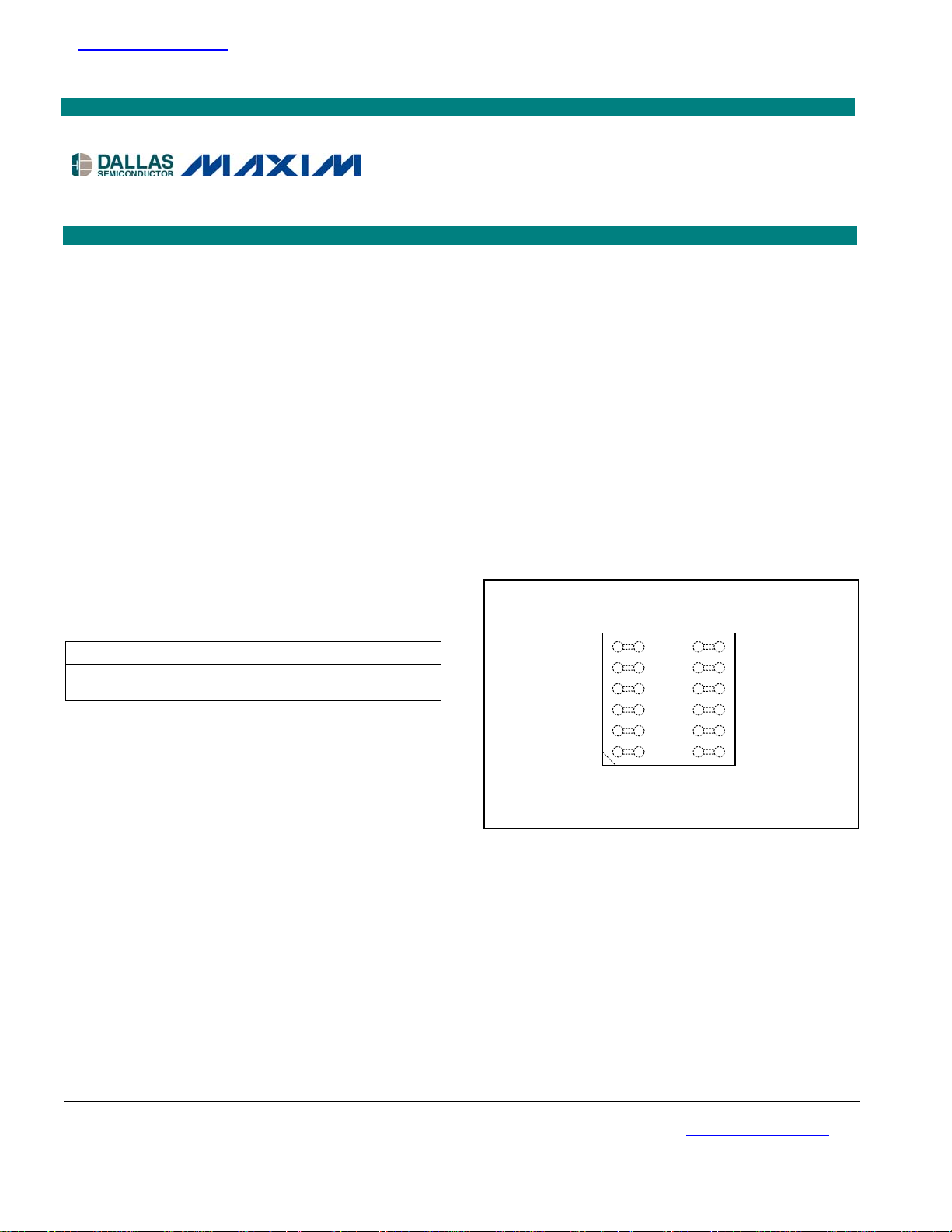
PIN CONFIGURATION
TOP VIEW
GND
A B C D
SCL
SDA
A0
OSC
N.C.
GND
6
5
4
3
2
1
BGA
F2
V
CC
F1
V
OSC
GND
GND
Note: Some revisions of this device may incorporate deviations from published specifications known as errata. Multiple revisions of any device
may be simultaneously available through various sales channels. For information about device errata, click here: www.maxim-ic.com/errata
.
1 of 16
REV: 072403
Page 2
DS4000 Digitally Controlled TCXO
ABSOLUTE MAXIMUM RATINGS
Voltage Range on Any Pin Relative to Ground -0.3V to +6.0V
Storage Temperature Range -55°C to +85°C
Operating Voltage Range V
= 5V ±5%
CC
Operating Temperature Range
Commercial 0°C to +70°C
Industrial -40°C to +85°C
Soldering Temperature See IPC/JEDEC J-STD-020A (2x max)
Stresses beyond those listed under “Absolute Maximum Ratings” may cause permanent damage to the device. These are stress ratings only,
and functional operation of the device at these or any other conditions beyond those indicated in the operational sections of the specifications is
not implied. Exposure to absolute maximum rating conditions for extended periods can affect device reliability.
RECOMMENDED DC OPERATING CONDITIONS
(VCC = 5V ±5%, over the operating temperature range.)
PARAMETER SYMBOL CONDITIONS MIN TYP MAX UNITS
Supply Voltage VCC (Notes 1, 2) 4.75 5.0 5.25 V
Oscillator Supply Voltage V
(Notes 1, 2) 4.75 5.0 5.25 V
OSC
Input Logic High VIH (Note 1) 2.2 VCC + 0.3 V
Input Logic Low VIL (Note 1) -0.3 +0.8 V
DC ELECTRICAL CHARACTERISTICS
(VCC = 5V ±5%, over the operating temperature range.)
PARAMETER SYMBOL CONDITIONS MIN TYP MAX UNITS
Active Supply Current ICC (Notes 3, 4) 1.5 2 mA
Active Oscillator Supply Current I
Output Logic High 2.4V IOH (Note 1) -1 mA
Output Logic Low 0.4V IOL (Note 1) 4 mA
Input Leakage ILI
I/O Leakage ILO
Temperature Conversion Time t
Note 1: All voltages are referenced to ground.
Note 2: For ±10% operating range, contact factory.
Note 3: Typical values are at +25°C and nominal supplies.
Note 4: These parameters are measured with the outputs disabled.
(Notes 3, 4) 3.5 5.5 mA
OSC
(Note 3) 250 300 ms
CONVT
1
1
mA
mA
2 of 16
Page 3
AC ELECTRICAL CHARACTERISTICS: TCXO
(VCC = 5V ±5%, over the operating temperature range.)
PARAMETER SYMBOL CONDITIONS MIN TYP MAX UNITS
Output Frequency
Frequency Stability vs.
Temperature
Frequency Stability vs. Voltage
F1
F
2
DF/T
DF/V
CMOS (Note 5) 10 20 MHz
-1.0 +1.0 ppm
A
(Note 6) ±1.0 ppm/V
DS4000 Digitally Controlled TCXO
Frequency Stability vs. Aging
F1, F2 Rise and Fall Time, 10% to
90%
DF/Yr
t
, tF 4 ns
R
±1.0 ppm/Yr
Max Output Capacitive Load CL 10 pF
Duty Cycle tW / t 40 50 60 %
10Hz -85
100Hz -115
Phase Noise f1 Output (Note 7)
1kHz -129
f
N
dBc/Hz
10kHz -134
100kHz -139
Note 5: F1 is the base frequency as defined by the package markings. F2 is a programmable frequency output. The output frequency of F2 is
derived from the base frequency, F
register. The minimum output frequency is F
Note 6: First year typical.
Note 7: 16.384MHz, 5V, +25°C with one of the two outputs enabled.
, by programming the F2 frequency select register and duty cycle (DC) bit in the TCXO control
1
/ (28 + 1) with DC = 0 and f1 / [2 x (28 + 1)] with DC = 1.
1
3 of 16
Page 4
DS4000 Digitally Controlled TCXO
AC ELECTRICAL CHARACTERISTICS—2-WIRE SERIAL INTERFACE
(VCC = 4.75 to 5.25V, TA = -40°C to +85°C)
PARAMETER SYMBOL CONDITION MIN TYP MAX UNITS
Fast mode 0 400
SCL Clock Frequency f
SCL
Standard mode 0 100
kHz
Bus Free Time Between
a STOP and START
Condition
Hold Time (Repeated)
START Condition
Low Period of SCL
Clock
High Period of SCL
Clock
Setup Time for a
Repeated START
Condition
Data Hold Time t
Data Setup Time t
t
BUF
t
HD:STA
t
LOW
t
HIGH
t
SU:STA
HD:DAT
SU:DAT
Fast mode 1.3
ms
Standard mode 4.7
Fast mode (Note 7) 0.6
Standard mode (Note 7) 4.0
ms
Fast mode 1.3
Standard mode 4.7
ms
Fast mode 0.6
ms
Standard mode 4.0
Fast mode 0.6
ms
Standard mode 4.7
Fast mode (Note 8) 0 0.9
ms
Standard mode (Note 8) 0 0.9
Fast mode (Note 9) 100
ns
Standard mode (Note 9) 250
Rise Time of Both SDA
and SCL
Fall Time of Both SDA
and SCL
Setup Time for STOP
Condition
Capacitive Load for
Each Bus Line
Input Capacitance
Note 7: After this period, the first clock pulse is generated.
Note 8: The maximum t
Note 9: A fast-mode device can be used in a standard mode system, but the requirement t
Note 10: C
the case if the device does not stretch the LOW period of the SCL signal. If such a device does stretch the LOW period of the SCL
signal, it must output the next data bit to the SDA line t
: Total capacitance of one bus line in pF.
B
has only to be met if the device does not stretch the LOW period (t
HD:DAT
tR
tF
t
SU:STO
CB
CI
Fast mode (Note 9) 20 + 0.1CB 300
Standard mode (Note 9) 20 + 0.1CB 1000
Fast mode (Note 10) 20 + 0.1CB 300
Standard mode (Note 10) 20 + 0.1CB 1000
Fast mode 0.6
Standard mode 4.0
(Note 10) 400 pF
5 pF
+ t
RMAX
4 of 16
(1000 + 250 = 1250ns) before the SCL line is released.
SU:DAT
) of the SCL signal.
LOW
>250ns must then be met. This is automatically
SU:DAT
ns
ns
ms
Page 5
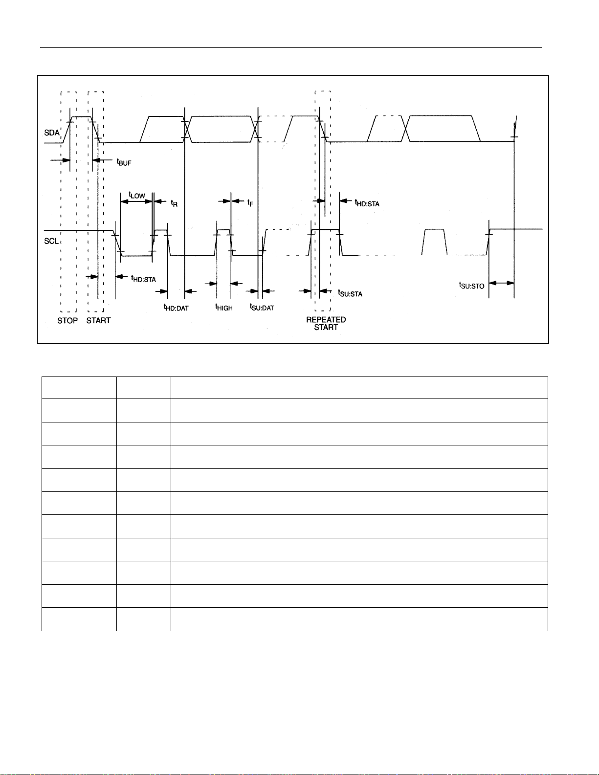
Figure 1. Timing Diagram
DS4000 Digitally Controlled TCXO
PIN DESCRIPTION
PIN NAME FUNCTION
1A, 1B, 1C,
1D, 2C, 2D
2A, 2B N.C. No Connection. (Do not connect to ground.)
3A, 3B GND
3C, 3D V
4A, 4B A0 2-Wire Slave Address Input. This pin is used to configure the slave address.
4C, 4D F1 DC-TCXO Frequency Output
5A, 5B SDA
5C, 5D VCC Power Supply. DC power is provided to the device on these pins.
6A, 6B SCL
6C, 6D F2 DC-TCXO Frequency Output
GND Ground. DC power is provided to the device on these pins.
Oscillator Ground. DC power is provided to the oscillator on these pins.
OSC
Oscillator Power Supply. DC power is provided to the oscillator on these pins.
OSC
2-Wire Serial-Data Input/Output. SDA is the input/output pin for the 2-wire serial
interface. The SDA pin is open drain and requires an external pullup resistor.
2-Wire Serial-Clock Input. SCL is used to synchronize data movement on the serial
interface. The SCL pin is open drain and requires an external pullup resistor.
5 of 16
Page 6

DS4000 Digitally Controlled TCXO
DETAILED DESCRIPTION
The DS4000 digitally controlled temperature-compensated crystal oscillator (DC-TCXO) features a digital
temperature sensor, one fixed-frequency temperature-compensated square-wave output (F
temperature-compensated square-wave output (F
), and digital communication for frequency tuning (SDA, SCL).
2
Figure 2. Block Diagram
VCC
SDA
SCL
A0
2-WIRE
SERIAL
INTERFACE
DS4000
GND
V
OSC
TEMPERATURE-
COMPENSATED
OSCILLATOR
TEMPERATURE
OSC
GND
CRYSTAL
DIGITAL
SENSOR
), one programmable
1
F
2
F
1
6 of 16
Page 7

DS4000 Digitally Controlled TCXO
TEMPERATURE-COMPENSATED CRYSTAL OSCILLATOR
The DS4000 can either function as a standalone TCXO or as a digitally controlled TCXO. When used as a
standalone TCXO, the only requirements needed to function properly are power, ground, and an output. However,
the 2-wire interface must be used to tune (push and pull) the crystal.
The DS4000 is capable of supplying two different outputs, F
is the base frequency of the crystal unit inside of the device. The output type is a CMOS square wave.
1) F
1
is a programmable frequency output. The frequency select register can program this output to an integer
2) F
2
division of the base (F
division of F
.
1
) frequency. The duty cycle (DC) bit determines if the output is an n + 1 or a 2(n + 1)
1
and F2.
1
FREQUENCY SELECT REGISTER (FSR) (5Dh)
F
2
Bit
7 6 5 4 3 2 1 0
Name D7 D6 D5 D4 D3 D2 D1 D0
Default 0 0 0 0 0 0 0 0
F
= F1 / (FSR value + 1); with DC = 0
2
F
= F1 / [2 x (FSR value + 1)]; with DC = 1
2
TCXO CONTROL REGISTER (60h)
Bit
7 6 5 4 3 2 1 0
Name X X X X F2OE F1OE FT DC
Default 0 0 0 0 0 0 0 0
DC, Duty Cycle Bit: If 50% duty cycle is desired, then this bit must be set to logic 1. The default condition at
power-up is logic 0.
: This bit must be programmed by the user to 0.
F
T
F
OE, F1 Output Enable Bit: This bit allows the user to disable/enable the F1 output.
1
OE, F2 Output Enable Bit: This bit allows the user to disable/enable the F2 output.
F
2
7 of 16
Page 8

DS4000 Digitally Controlled TCXO
DIGITAL TUNING THE BASE CRYSTAL FREQUENCY
When using the 2-wire interface for tuning the base frequency, the frequency tuning register is used. The frequency
tuning register contains two’s complement data. The data is used to add or subtract an offset from the crystal
loading register. When the tuning register is programmed with a value, the next temperature-update cycle sums the
programmed value with the factory-compensated value. This allows the user/system to digitally control the base
frequency by a microcontroller using the 2-wire protocol.
FREQUENCY TUNING REGISTER (66h)
Bit
Name SIGN FO6 FO5 FO4 FO3 FO2 FO1 FO0
Default 0 0 0 0 0 0 0 0
FOS[6:0], Frequency Offset: These bits are used to tune the base crystal frequency. Each bit represents
approximately 0.08ppm and, therefore, for a value of 07FH, pushes or pulls the base frequency by approximately
10.16ppm.
SIGN, Sign Bit: This bit is used to determine whether to add or subtract the frequency offset from the crystal
loading.
Table 1. Frequency Tuning Relationship
7 6 5 4 3 2 1 0
CALCULATED
FREQUENCY OFFSET
(ppm)
-10.16 0111 1111 7Fh
-8.00 0110 0100 64h
-5.28 0100 0010 42h
-1.84 0001 0111 17h
-0.08 0000 0001 01h
0.0 0000 0000 00h
+0.08 1111 1111 FFh
+1.84 1110 1000 E8h
+5.28 1011 0011 B3h
+8.00 1001 1100 9Ch
+10.16 1000 0000 80h
DIGITAL DATA
(Binary)
DIGITAL DATA
(hex)
8 of 16
Page 9

DS4000 Digitally Controlled TCXO
DIGITAL TEMPERATURE SENSOR
The digital temperature sensor provides 10-bit temperature readings that indicate the temperature of the device.
Temperature readings are communicated from the DS4000 over a 2-wire serial interface. No additional
components are required. The DS4000 has an external address bit that allows a user to choose the slave address
from two possible values.
The factory-calibrated temperature sensor requires no external components. Upon power-up, the DS4000 starts
performing temperature conversions with a resolution of 10 bits (+0.25°C resolution). Following an 8-bit command
protocol, temperature data can be read over the 2-wire interface. The host can periodically read the value in the
temperature register, which contains the last completed conversion. As conversions are performed in the
background, reading the temperature register does not affect the conversion in progress.
READING TEMPERATURE
The DS4000 measures temperature through the use of an on-chip temperature-measurement technique with an
operation range from 0°C to +70°C (commercial) or -40°C to +85°C (industrial). The device performs continuous
conversions with the most recent result being stored in the temperature register. The digital temperature is
retrieved from the temperature register using the READ TEMPERATURE command, as described in detail in the
following paragraphs.
Table 2 shows the exact relationship of output data to measured temperature. The data is transmitted serially over
the 2-wire serial interface, MSB first. The MSB of the temperature register contains the “sign” (S) bit, denoting
whether the temperature is positive or negative. For Fahrenheit usage, a lookup table or conversion routine must
be used.
TEMPERATURE/DATA RELATIONSHIP (UNIT = °C)
MSB (64h)
BIT 7 BIT 6 BIT 5 BIT 4 BIT 3 BIT 2 BIT 1 BIT 0
S 26 2
LSB (65h)
BIT 7 BIT 6 BIT 5 BIT 4 BIT 3 BIT 2 BIT 1 BIT 0
2-1 2
-2
0 0 0 0 0 0
Table 2. Temperature/Data Relationship
5
2
4
2
3
2
2
2
1
2
0
TEMPERATURE
(°C)
DIGITAL OUTPUT
(Binary)
DIGITALOUTPUT
(hex)
+85 0101 0101 0000 0000 5500h
+75 0100 1011 0000 0000 4B00h
+0.5 0000 0000 1000 0000 0080h
0 0000 0000 0000 0000 0000h
-0.5 1111 1111 1000 0000 FF80h
-20 1110 1100 0000 0000 EC00h
Note: Internal power dissipation raises the temperature above the ambient. The delta between ambient and the die temperature depends on
power consumption, PC board layout, and airflow.
-40 1101 1000 0000 0000 D800h
9 of 16
Page 10

DS4000 Digitally Controlled TCXO
READ TEMPERATURE COMMAND
This command reads the last temperature conversion result from the temperature register in the format described
in the Reading Temperature section. If an application can accept temperature resolutions of +1.0°C, then the
master can read the first data byte and follow with a NACK and STOP. For higher resolution, both bytes must be
read.
Table 3. Command Set
2-WIRE BUS DATA
INSTRUCTION FUNCTION PROTOCOL
Frequency Select
Register (Note 1)
TCXO Control
Register (Note 1)
Read Temperature
(Note 2)
Frequency Tuning
Register (Note 2)
Defines F
Enables/disables F1 and F2;
sets duty cycle of F
output frequency 5Dh
2
2
60h
Reads 10-bit temperature register 64h Read 1 or 2 data bytes
Digitally adds/subtracts an offset
from oscillator
66h
AFTER ISSUING
PROTOCOL
Read or write 1 data
byte
Read or write 1 data
byte
Read or write 1 data
byte
Note 1: The slave does not increment the internal address pointer between instructions. The address pointer must be reinitialized after each
Note 2. If the user only desires 8-bit thermometer readings, the master can read one data byte, and follow with a NACK and STOP. If higher
access.
resolution is required, both bytes must be read.
10 of 16
Page 11

DS4000 Digitally Controlled TCXO
2-WIRE SERIAL INTERFACE
The DS4000 supports a bidirectional 2-wire serial bus and data transmission protocol. The bus must be controlled
by a master device, which generates the serial clock (SCL), controls the bus access, and generates the START
and STOP conditions. The DS4000 operates as a slave on the 2-wire bus. The DS4000 works in a regular mode
(100kHz clock rate) and a fast mode (400kHz clock rate), which are defined within the bus specifications.
Connections to the bus are made by the open-drain I/O signals SDA and SCL.
The following bus protocol has been defined (Figure 3):
§ Data transfer can be initiated only when the bus is not busy.
§ During data transfer, the data signal must remain stable whenever the clock signal is HIGH. Changes in the
data signal while the clock signal is HIGH are interpreted as control signals.
Accordingly, the following bus conditions have been defined:
Bus Not Busy: Both data and clock signals remain HIGH.
Start Data Transfer: A change in the state of the data signal, from HIGH to LOW, while the clock line is HIGH,
defines the START condition.
Stop Data Transfer: A change in the state of the data signal, from LOW to HIGH, while the clock line is HIGH,
defines the STOP condition.
Data Valid: The state of the data signal represents valid data when, after a START condition, the data signal is
stable for the duration of the HIGH period of the clock signal. The data on the line must be changed during the
LOW period of the clock signal. There is one clock pulse per bit of data.
Each data transfer is initiated with a START condition and terminated with a STOP condition. The number of data
bytes transferred between START and STOP conditions is not limited and is determined by the master device. The
information is transferred byte-wise and each receiver acknowledges with a ninth bit.
Acknowledge: Each receiving device, when addressed, is required to generate an acknowledge after reception of
each byte. The master device must generate an extra clock pulse that is associated with this acknowledge bit.
A device that acknowledges must pull down the serial data (SDA) signal during the acknowledge clock pulse in
such a way that the SDA signal is stable LOW during the HIGH period of the acknowledge-related clock pulse. Of
course, setup and hold times must be taken into account. A master must signal an end-of-data to the slave by not
generating an acknowledge bit on the last byte that has been clocked out of the slave. In this case, the slave must
leave the data signal HIGH to enable the master to generate the STOP condition.
11 of 16
Page 12

Figure 3. Data Transfer On 2-Wire Serial Bus
SDA
MSB
SLAVE
ADDRESS
R/W BIT
ACKNOWLEDGEMENT
SIGNAL FROM
RECEIVER
DS4000 Digitally Controlled TCXO
ACKNOWLEDGEMENT
SIGNAL FROM
RECEIVER
SCL
START
CONDITION
123-56789
ACK ACK
REPEATED IF
MORE BYTES ARE
TRANSFERRED
893-712
STOP CONDITION
OR REPEATED
START CONDITION
DATA TRANSFER
Figures 4 and 5 detail how data transfer is accomplished on the 2-wire bus.
Depending on the R/W bit in the transmission protocols as shown, two types of data transfer are possible:
1) Data transfer from a master transmitter to a slave receiver. The first byte transmitted by the master is the
slave address. Next follows a number of data bytes. The slave returns an acknowledge bit after each received
byte. Data is transferred with the most significant bit (MSB) first.
2) Data transfer from a slave transmitter to a master receiver. The master transmits the first byte (the slave
address). The slave then returns an acknowledge bit. Next follows a number of data bytes transmitted by the
slave to the master. The master returns an acknowledge bit after all received bytes other than the last byte. At
the end of the last received byte, a “not acknowledge” is returned. The master device generates all of the serial
clock pulses and the START and STOP conditions. A transfer is ended with a STOP condition or with a
repeated START condition. Since a repeated START condition is also the beginning of the next serial transfer,
the bus is not released.
12 of 16
Page 13

DS4000 Digitally Controlled TCXO
SLAVE ADDRESS
The slave address is the first byte received following the START condition generated by the master device. The
address byte consists of a 7-bit slave address and the R/
100010A
, where A0 is externally hardwired to a HIGH or LOW state. This allows design flexibility to set the slave’s
0
address to one of two possible address locations. The last bit following the slave address is the direction bit (R/
and defines the operation to be performed by the master, transmit data (R/
Following the START condition, the DS4000 monitors the SDA bus by checking the slave address being
transmitted. Upon receiving the proper slave address and R/
on the SDA line regardless of the operation mode.
The DS4000 can operate in the following two modes:
1) Slave Receiver Mode: Serial data and clock are received through SDA and SCL. After each byte is received,
an acknowledge bit is transmitted. START and STOP conditions are recognized as the beginning and end of a
serial transfer. Address recognition is performed by the hardware after reception of the slave address and
direction bit (Figure 4).
2) Slave Transmitter Mode: The first byte is received and handled as in the slave receiver mode. However, in
this mode, the direction bit indicates that the transfer direction is reversed. Serial data is transmitted on SDA by
the DS4000 while the serial clock is input on SCL. START and STOP conditions are recognized as the
beginning and end of a serial transfer (Figure 5).
Figure 4. Data Write—Slave Receiver Mode
<SLAVE ADDRESS>
<DATA ADDRESS> <DATA (n)>
R/W
S 100010A0 0 A XXXXXXXX A XXXXXXXX A P
S = START
A = ACKNOWLEDGE
P = STOP
Figure 5. Data Read—Slave Transmitter Mode
<SLAVE ADDRESS>
S 100010A0 1 A XXXXXXXX A XXXXXXXX A XXXXXXXX A XXXXXXXX AP
R/W
<DATA (n)>
<DATA (n + 1)> <DAT A (n + 2)>
W direction bit. The DS4000 slave address is set to
W)
W = 0), or receive data (R/W = 1).
W bit, the slave device outputs an acknowledge signal
<DATA (n + X)>
S = START
A = ACKNOWLEDGE
P = STOP
A = NOT ACKNOWLEDGE
13 of 16
Page 14

SELECTOR GUIDE
DS4000 Digitally Controlled TCXO
PART TEMP RANGE PIN-PACKAGE TOP MARK
DS4000A0/WBGA 0°C to +70°C
DS4000A0N/WBGA -40°C to +85°C
DS4000CW/WBGA 0°C to +70°C
DS4000CWN/WBGA -40°C to +85°C
24 BGA DS4000A0 10.00000
24 BGA
DS4000A0
###XX N
24 BGA DS4000CW 12.80000
24 BGA
DS4000CW
###XX N
FREQUENCY
DESIGNATOR (MHz)
10.00000
12.80000
DS4000D0/WBGA 0°C to +70°C 24 BGA DS4000D0 13.00000
DS4000D0N/WBGA -40°C to +85°C 24 BGA
DS4000D0
###XX N
13.00000
DS4000EC/WBGA 0°C to +70°C 24 BGA DS4000EC 14.31818
DS4000ECN/WBGA -40°C to +85°C 24 BGA
DS4000EC
###XX N
14.31818
DS4000G0/WBGA 0°C to +70°C 24 BGA DS4000G0 16.00000
DS4000G0N/WBGA -40°C to +85°C 24 BGA
DS4000G0
###XX N
16.00000
DS4000GF/WBGA 0°C to +70°C 24 BGA DS4000GF 16.38400
DS4000GFN/WBGA -40°C to +85°C 24 BGA
DS4000GF
###XX N
16.38400
DS4000GW/WBGA 0°C to +70°C 24 BGA DS4000GW 16.80000
DS4000GWN/WBGA -40°C to +85°C 24 BGA
DS4000GW
###XX N
16.80000
DS4000KI/WBGA 0°C to +70°C 24 BGA DS4000KI 19.44000
DS4000KIN/WBGA -40°C to +85°C 24 BGA
DS4000KI
###XX N
19.44000
14 of 16
Page 15

DS4000 Digitally Controlled TCXO
PACKAGE INFORMATION
(The package drawing(s) in this data sheet may not reflect the most current specifications. For the latest package outline information, go to
www.maxim-ic.com/DallasPackInfo
NOTE: THE BGA IS SOLDER-MASKED DEFINED.
.)
15 of 16
Page 16

DS4000 Digitally Controlled TCXO
PACKAGE INFORMATION (continued)
(The package drawing(s) in this data sheet may not reflect the most current specifications. For the latest package outline information, go to
www.maxim-ic.com/DallasPackInfo
PAD: 0.85mm
.)
1.27
SOLDERMASK: 0.60mm
1.27
8.89
DIMENSIONS IN MILLIMETERS
Maxim/Dallas Semiconductor cannot assume responsibility for use of any circuitry other than circuitry entirely embodied in a Maxim/Dallas Semiconductor product.
No circuit patent licenses are implied. Maxim/Dallas Semiconductor reserves the right to change the circuitry and specifications without notice at any time.
Maxim Integrated Products, 120 San Gabriel Drive, Sunnyvale, CA 94086 408-737-7600
© 2003 Maxim Integrated Products · Printed USA
16 of 16
 Loading...