

Page 1

General Description
The DS3234 is a low-cost, extremely accurate SPI™ bus
real-time clock (RTC) with an integrated temperaturecompensated crystal oscillator (TCXO) and crystal. The
DS3234 incorporates a precision, temperature-compensated voltage reference and comparator circuit to monitor V
CC
. When VCCdrops below the power-fail voltage
(V
PF
), the device asserts the RST output and also dis-
ables read and write access to the part when V
CC
drops
below both V
PF
and V
BAT
. The RST pin is monitored as
a pushbutton input for generating a reset externally. The
device switches to the backup supply input and maintains accurate timekeeping when main power to the
device is interrupted. The integration of the crystal resonator enhances the long-term accuracy of the device
as well as reduces the piece-part count in a manufacturing line. The DS3234 is available in commercial and
industrial temperature ranges, and is offered in an
industry-standard 300-mil, 20-pin SO package.
The DS3234 also integrates 256 bytes of battery-backed
SRAM. In the event of main power loss, the contents of
the memory are maintained by the power source connected to the V
BAT
pin. The RTC maintains seconds,
minutes, hours, day, date, month, and year information.
The date at the end of the month is automatically adjusted for months with fewer than 31 days, including corrections for leap year. The clock operates in either the
24-hour or 12-hour format with AM/PM indicator. Two
programmable time-of-day alarms and a programmable
square-wave output are provided. Address and data are
transferred serially by an SPI bidirectional bus.
Applications
Servers Utility Power Meters
Telematics GPS
Features
♦ Accuracy ±2ppm from 0°C to +40°C
♦ Accuracy ±3.5ppm from -40°C to +85°C
♦ Battery Backup Input for Continuous
Timekeeping
♦ Operating Temperature Ranges
Commercial: 0°C to +70°C
Industrial: -40°C to +85°C
♦ Low-Power Consumption
♦ Real-Time Clock Counts Seconds, Minutes,
Hours, Day, Date, Month, and Year with Leap Year
Compensation Valid Up to 2099
♦ Two Time-of-Day Alarms
♦ Programmable Square-Wave Output
♦ 4MHz SPI Bus Supports Modes 1 and 3
♦ Digital Temp Sensor Output: ±3°C Accuracy
♦ Register for Aging Trim
♦ RST Input/Output
♦ 300-Mil, 20-Pin SO Package
♦ Underwriters Laboratory (UL) Recognized
DS3234
Extremely Accurate SPI Bus RTC with
Integrated Crystal and SRAM
______________________________________________
Maxim Integrated Products
1
Rev 1; 7/07
For pricing, delivery, and ordering information, please contact Maxim/Dallas Direct! at
1-888-629-4642, or visit Maxim’s website at www.maxim-ic.com.
Ordering Information
SPI is a trademark of Motorola, Inc.
Typical Operating Circuit
#
Denotes a RoHS-compliant device that may include lead that
is exempt under the RoHS requirements. Lead finish is JESD97
Category e3, and is compatible with both lead-based and
lead-free soldering processes. A "#" anywhere on the top mark
denotes a RoHS-compliant device.
TOP VIEW
20
19
18
17
16
15
14
13
1
2
3
4
5
6
7
8
SCLK
DOUT
SCLK
DINV
CC
32kHz
N.C.
CS
V
BAT
GND
N.C.
N.C.N.C.
N.C.
RST
INT/SQW
12
11
9
10
N.C.
N.C.N.C.
N.C.
SO
DS3234
Pin Configuration
PART TEMP RANGE
DS3234S# 0°C to +70°C 20 SO DS3234S
DS3234SN# -40°C to +85°C 20 SO DS3234SN
PINPACKAGE
TOP
MARK
V
V
CC
SS
SCLK
MOSI
MISO
RST
CPU
PUSH-
BUTTON
RESET
CS
SCLK
DIN
DOUT
RST
N.C.
N.C.
N.C.
N.C.
N.C.
CC
V
CC
INT/SQW
DS3234
GND
32kHz
V
BAT
N.C.
N.C.
N.C.
N.C.
V
PU
Page 2
DS3234
Extremely Accurate SPI Bus RTC with
Integrated Crystal and SRAM
2 _____________________________________________________________________
ABSOLUTE MAXIMUM RATINGS
RECOMMENDED DC OPERATING CONDITIONS
(TA= -40°C to +85°C, unless otherwise noted.) (Notes 1, 2)
Stresses beyond those listed under “Absolute Maximum Ratings” may cause permanent damage to the device. These are stress ratings only, and functional
operation of the device at these or any other conditions beyond those indicated in the operational sections of the specifications is not implied. Exposure to
absolute maximum rating conditions for extended periods may affect device reliability.
Voltage Range on Any Pin Relative to Ground......-0.3V to +6.0V
Operating Temperature Range
(noncondensing) .............................................-40°C to +85°C
Junction Temperature......................................................+125°C
Storage Temperature Range ...............................-40°C to +85°C
Soldering Temperature
(leads, 10s) ...........................................................+260°C/10s
Soldering Temperature (reflow, 2 times max) .......See IPC/JEDEC
J-STD-020 Specification
ELECTRICAL CHARACTERISTICS
(VCC= 2.0V to 5.5V, VCC= active supply (see Table 1), TA= -40°C to +85°C, unless otherwise noted.) (Typical values are at VCC=
3.3V, V
BAT
= 3.0V, and TA= +25°C, unless otherwise noted. TCXO operation guaranteed from 2.3V to 5.5V on VCCand 2.3V to 3.8V on
V
BAT
.) (Notes 1, 2)
Supply Voltage
Logic 1 Input CS, SCLK, DIN V
Logic 0 Input CS, SCLK, DIN,
RST
Pullup Voltage INT/SQW V
PARAMETER SYMBOL CONDITIONS MIN TYP MAX UNITS
V
CC
V
BAT
IH
V
PU
2.0V ≤ VCC ≤ 3.63V -0.3
IL
3.63V < VCC ≤ 5.5V -0.3 +0.7
VCC = 0V 5.5 V
2.0 3.3 5.5
2.0 3.0 3.8
0.7 x
V
CC
VCC +
0.3
+0.2 x
V
CC
V
V
V
Active Supply Current I
Standby Supply Current I
Temperature Conversion Current I
Power-Fail Voltage V
V
BAT
(VCC = 2.0V to 5.5V, TA = -40°C to +85°C, unless otherwise noted.) (Notes 1 and 2)
Logic 1 Output, 32kHz
I
OH
I
OH
I
OH
PARAMETER SYMBOL CONDITIONS MIN TYP MAX UNITS
VCC = 3.63V 400
V
= 5.5V 700
CC
VCC = 3.63V 120
V
= 5.5V 160
CC
VCC = 3.63V 500
V
= 5.5V 600
CC
2.45 2.575 2.70 V
25 100 nA
0.85 x V
CC
Leakage Current I
= -500µA
= -250µA
= -125µA
CCA
CCS
CCSCONV
PF
BATLKG
V
OH
SCLK = 4MHz, BSY = 0
(Notes 3, 4)
CS = VIH, 32kHz output off,
SQW output off
(Note 4)
SPI bus inactive, 32kHz
output off, SQW output off
VCC > 3.63V,
3.63V > V
2.7V > (V
(BB32kHz = 1)
CC
CC
> 2.7V,
or V
BAT
) > 2.0V
µA
µA
µA
V
Page 3
DS3234
Extremely Accurate SPI Bus RTC with
Integrated Crystal and SRAM
_____________________________________________________________________ 3
ELECTRICAL CHARACTERISTICS (continued)
(VCC= 2.0V to 5.5V, VCC= active supply (see Table 1), TA= -40°C to +85°C, unless otherwise noted.) (Typical values are at VCC=
3.3V, V
BAT
= 3.0V, and TA= +25°C, unless otherwise noted. TCXO operation guaranteed from 2.3V to 5.5V on VCCand 2.3V to 3.8V on
V
BAT
.) (Notes 1, 2)
ELECTRICAL CHARACTERISTICS
(VCC= 0V, V
BAT
= 2.0V to 3.8V, TA= -40°C to +85°C, unless otherwise noted.) (Note 1)
Logic 0 Output, 32kHz V
Logic 1 Output, DOUT V
Logic 0 Output, DOUT, INT/SQW V
Logic 0 Output, RST V
Output Leakage Current 32kHz,
INT/SQW, DOUT
Input Leakage DIN, CS, SCLK I
RST Pin I/O Leakage I
TCXO (V
Output Frequency f
PARAMETER SYMBOL CONDITIONS MIN TYP MAX UNITS
I
= 1mA 0.4 V
OL
I
= -1.0mA 0.85 x V
OH
I
= 3mA 0.4 V
OL
I
= 1.0mA 0.4 V
OL
CC
Output high impedance -1 0 +1 µA
-1 +1 µA
RST high impedance (Note 5) -200 +10 µA
V
= 3.3V or V
CC
= 3.3V 32.768 kHz
BAT
= 2.3V to 5.5V, V
CC
OL
OH
OL
OL
I
LO
LI
OL
= 2.3V to 3.8V, TA = -40°C to +85°C, unless otherwise noted.) (Notes 1 and 2)
BAT
OUT
V
0°C to +40°C -2 +2
Frequency Stability vs.
Temperature
Δf/f
OUT
V
V
CC
BAT
= 3.3V or
= 3.3V
-40°C to 0°C and
+40°C to +85°C
-3.5 +3.5
ppm
Frequency Stability vs. Voltage Δf/V 1 ppm/V
-40°C 0.7
Trim Register Frequency
Sensitivity per LSB
Δf/LSB Specified at:
+25°C 0.1
+70°C 0.4
ppm
+85°C 0.8
Temperature Accuracy Temp -3 +3 °C
Crystal Aging Δf/f
OUT
After reflow,
not production tested
First year ±1.0
0–10 years ±5.0
ppm
Battery Current
(Note 4)
Temperature Conversion Current I
Data-Retention Current I
PARAMETER SYMBOL CONDITIONS MIN TYP MAX UNITS
I
BAT
TC
BATTC
V
= 3.4V 1.5 2.3
EOSC = 0, BBSQW = 0
EOSC = 0, BBSQW = 0 400 µA
EOSC = 1 100 nA
BAT
= 3.8V 1.5 2.5
V
BAT
µA
Page 4
DS3234
Extremely Accurate SPI Bus RTC with
Integrated Crystal and SRAM
4 _____________________________________________________________________
AC ELECTRICAL CHARACTERISTICS
(VCC= 2.0V to 5.5V, TA= -40°C to +85°C, unless otherwise noted.) (Note 1)
POWER-SWITCH CHARACTERISTICS
(TA= -40°C to +85°C)
CAPACITANCE
(TA= +25°C)
PARAMETER SYMBOL CONDITIONS MIN TYP MAX UNITS
SCLK Clock Frequency f
Data to SCLK Setup t
SCLK to Data Hold t
SCLK to CS Setup t
SCLK to Data Valid (Note 6) t
SCLK Low Time t
SCLK High Time t
SCLK Rise and Fall tR, t
CS to SCLK Setup t
SCLK to CS Hold t
CS Inactive Time t
CS to Output High Impedance t
Pushbutton Debounce PBDB 250 ms
Reset Active Time t
Oscillator Stop Flag (OSF) Delay t
Temperature Conversion Time t
SCL
DC
CDH
CCS
CDD
CL
CH
CC
CCH
CWH
CDZ
RST
OSF
CONV
2.7V ≤ VCC ≤ 5.5V 4
2.0V ≤ V
2.7V ≤ VCC ≤ 5.5V 80
2.0V ≤ V
2.7V ≤ VCC ≤ 5.5V 110
2.0V ≤ V
2.7V ≤ VCC ≤ 5.5V 110
2.0V ≤ V
F
2.7V ≤ VCC ≤ 5.5V 100
2.0V ≤ V
(Note 7) 40 ns
(Note 8) 100 ms
< 2.7V 2
CC
30 ns
30 ns
30 ns
< 2.7V 160
CC
< 2.7V 220
CC
< 2.7V 220
CC
400 ns
< 2.7V 200
CC
250 ms
125 200 ms
MHz
ns
ns
ns
200 ns
ns
400 ns
VCC Fall Time; V
V
PF(MIN)
VCC Rise Time; V
V
PF(MAX)
Recovery at Power-Up t
PARAMETER SYMBOL CONDITIONS MIN TYP MAX UNITS
to
PF(MAX)
PF(MIN)
to
t
VCCF
t
VCCR
REC
(Note 9) 125 300 ms
Capacitance on All Input Pins C
Capacitance on All Output Pins C
PARAMETER SYMBOL CONDITIONS MIN TYP MAX UNITS
(Note 10) 10 pF
IN
Outputs high impedance (Note 10) 10 pF
IO
300 µs
0µs
Page 5
DS3234
Extremely Accurate SPI Bus RTC with
Integrated Crystal and SRAM
_____________________________________________________________________ 5
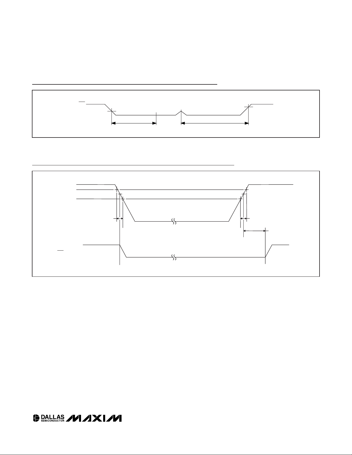
Pushbutton Reset Timing
Power-Switch Timing
Note 1: Limits at -40°C are guaranteed by design and not production tested.
Note 2: All voltages are referenced to ground.
Note 3: Measured at V
IH
= 0.8 x VCCor VIL= 0.2 x VCC, 10ns rise/fall time, DOUT = no load.
Note 4: Current is the averaged input current, which includes the temperature conversion current. CRATE1 = CRATE0 = 0.
Note 5: The RST pin has an internal 50kΩ (nominal) pullup resistor to V
CC
.
Note 6: Measured at V
OH
= 0.8 x VCCor VOL= 0.2 x VCC. Measured from the 50% point of SCLK to the VOHminimum of DOUT.
Note 7: With 50pF load.
Note 8: The parameter t
OSF
is the period of time the oscillator must be stopped for the OSF flag to be set over the voltage range of
0V ≤ V
CC
≤ V
CC(MAX)
and 2.3V ≤ V
BAT
≤ V
BAT(MAX)
.
Note 9: This delay only applies if the oscillator is enabled and running. If the EOSC bit is 1, t
REC
is bypassed and RST immediately
goes high.
Note 10: Guaranteed by design and not production tested.
WARNING: Negative undershoots below -0.3V while the part is in battery-backed mode may
cause loss of data.
V
PF(MAX)
V
PF(MIN)
RST
PB
DB
t
RST
V
CC
t
VCCF
V
PF
V
PF
t
VCCR
t
REC
RST
Page 6
DS3234
Extremely Accurate SPI Bus RTC with
Integrated Crystal and SRAM
6 _____________________________________________________________________
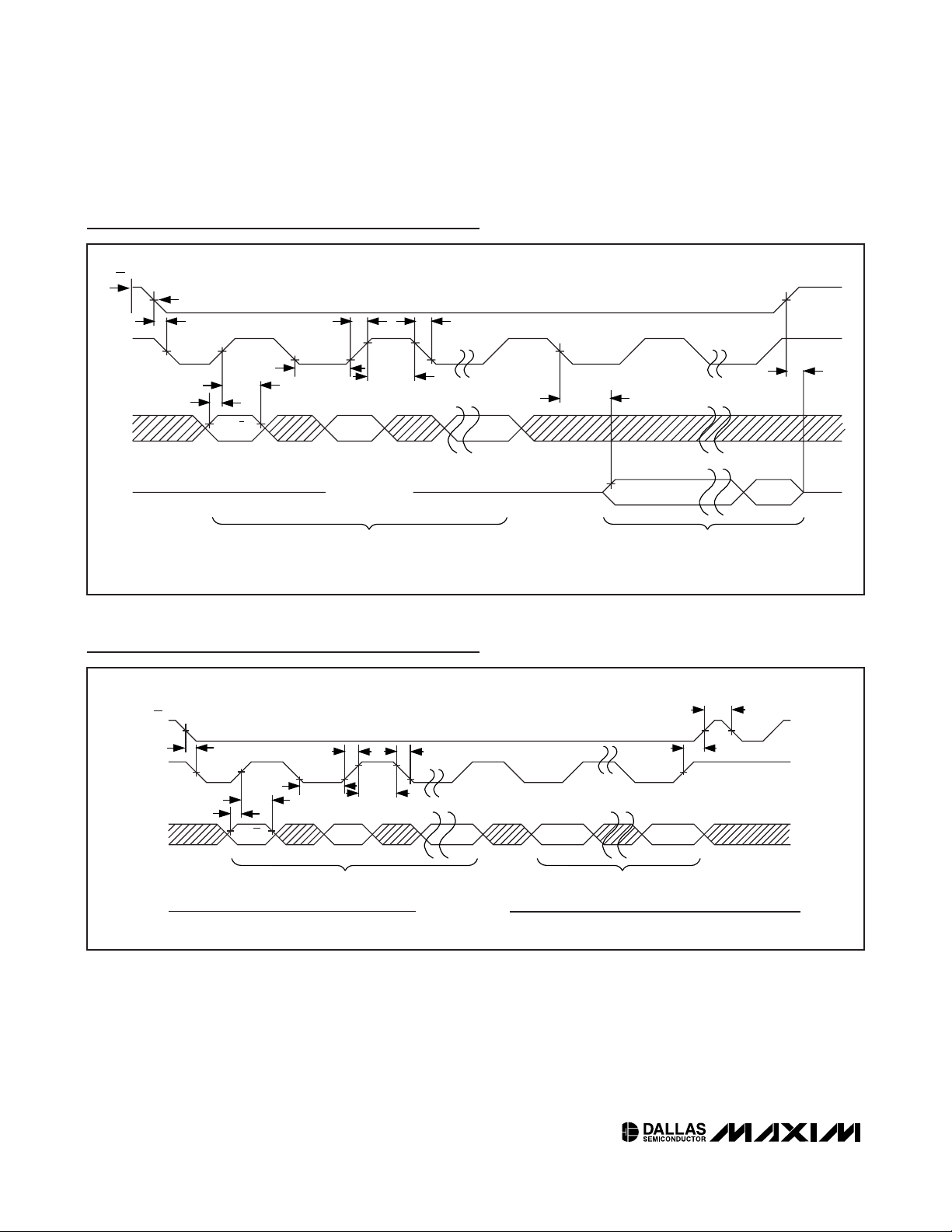
Timing Diagram—SPI Read Transfer
Timing Diagram—SPI Write Transfer
t
CS
CCS
t
SCLK
DIN
DOUT
NOTE: SCLK CAN BE EITHER POLARITY, SHOWN FOR CPOL = 1.
SCLK
CC
t
DC
W/R
CS
t
CC
t
t
CL
t
CDH
WRITE ADDRESS BYTE
t
R
A6
HIGH IMPEDANCE
R
t
F
t
t
CH
t
CDD
A0
D7
READ DATA BYTE
D0
CDZ
t
CWH
t
t
F
CCH
t
DOUT
DIN
CL
t
t
DC
W/R
CDH
WRITE ADDRESS BYTE
t
CH
A6
A0
HIGH IMPEDANCE
D7 D0
WRITE DATA BYTE
Page 7

DS3234
Extremely Accurate SPI Bus RTC with
Integrated Crystal and SRAM
_____________________________________________________________________
7
Typical Operating Characteristics
(VCC= +3.3V, TA = +25°C, unless otherwise noted.)
STANDBY SUPPLY CURRENT
vs. SUPPLY VOLTAGE
150
RST ACTIVE
125
100
75
50
SUPPLY CURRENT (μA)
25
0
2.3
3.3 3.8
VCC (V)
INPUTS = GND
4.8
4.32.8
BATTERY CURRENT
vs. TEMPERATURE
850
VCC = 0V
BB32kHz = 0
800
BBSQW = 0
750
700
SUPPLY CURRENT (nA)
650
600
-40
-20
0
TEMPERATURE (°C)
V
= 3.4V
BAT
V
= 3.0V
BAT
20
6040
BATTERY CURRENT
vs. SUPPLY VOLTAGE
2600
VCC = 0V
2350
DS3234 toc01
SUPPLY CURRENT (nA)
5.3
BB32kHz = 0
2100
1850
1600
1350
1100
850
600
2.3
SUPPLY VOLTAGE (V
FREQUENCY DEVIATION
vs. TEMPERATURE vs. AGING VALUE
65
DS3234 toc03
80
55
45
35
25
15
5
-5
-15
FREQUENCY DEVIATION (ppm)
-25
-35
-45
-40
-20
BBSQW = 1
BBSQW = 0
2.8
AGING = -33
AGING = 0
AGING = 127
AGING = 32
020
TEMPERATURE (°C)
40
3.3
)
BAT
AGING = -128
60
DS3234 toc02
3.8
DS3234 toc04
80
I
vs. DOUT LOAD
CCA
500
450
400
350
300
SUPPLY CURRENT (μA)
250
200
0
10
CAPACITANCE (pF)
SCLK = 4MHz
20
30
DS3234 toc05
40
Page 8

DS3234
Extremely Accurate SPI Bus RTC with
Integrated Crystal and SRAM
8 _____________________________________________________________________
Pin Description
PIN NAME FUNCTION
1 CS Active-Low Chip Select Input. Used to select or deselect the device.
2, 7–14 N.C. No Connection. Not connected internall y. Must be connected to ground.
3 32kHz
4 VCC DC Power Pin for Primary Power Supply. This pin should be decoupled using a 0.1μF to 1.0μF capacitor.
5 INT/SQW
6 RST
15 GND Ground
16 V
17 DIN SPI Data Input. Used to sh ift address and data into the device.
18, 20 SCLK
19 DOUT SPI Data Output. Data is output on th is pin when the device i s in read mode; CMOS push-pull driver.
32kHz Push-Pull Output. If disabled with either EN32kH z = 0 or BB32 kHz = 0, the state of the 32kHz pin will
be low.
Active-Low Interrupt or Square-Wave Output. This open-drain pin requires an external pullup resistor. It can
be left open if not u sed. This mu ltifunction pin i s determined by the state of the INTCN bit in the Control
Regi ster (0Eh). When INTCN is set to logic 0, this pin outputs a square wave and its frequency is
determined by RS2 and RS1 bits. When INTCN is set to logic 1, then a match between the timekeeping
registers and either of the alarm regi sters activates the INT/SQW pin (if the alarm is enabled). Because the
INTCN bit is set to logic 1 when power is first applied, the pin defaults to an interrupt output with alarms
disabled.
Active-Low Re set. Thi s pin i s an open-drain input/output. It indicates the status of V
V
specif ication. As VCC falls below VPF, the RST pin is driven low. When VCC exceeds VPF, for t
PF
pin is dr iven high impedance. The active- low, open-drain output is combined with a debounced pushbutton
input function. This pin can be activated by a pushbutton reset request. It has an internal 50k nominal value
pullup resistor to V
oscillator is disabled, t
Bac kup Power-Supply Input. If V
V
BAT
pin and the battery can cause improper operation. UL recognized to ensure again st reverse charging
BAT
when used with a lithium battery. Go to www.max im-ic.com/qa/info/ul.
SPI Clock Input. Used to control timing of data into and out of the device. Either clock polarity can be used.
The clock polarity is determined by the device based on the state of SCLK when CS goes low. Pins 18 and
20 are electrically connected together internally.
. No external pullup resistors should be connected. On first power-up, or if the crystal
CC
is b ypassed and RST immediately goes high.
RST
is not used, connect to ground. Diode s placed in series between the
BAT
relative to the
CC
, the RST
RST
Page 9

DS3234
Extremely Accurate SPI Bus RTC with
Integrated Crystal and SRAM
_____________________________________________________________________ 9
Detailed Description
The DS3234 is a TCXO and RTC with integrated crystal
and 256 bytes of SRAM. An integrated sensor periodically samples the temperature and adjusts the oscillator
load to compensate for crystal drift caused by temperature variations. The DS3234 provides user-selectable
sample rates. This allows the user to select a temperature sensor sample rate that allows for various temperature rates of change, while minimizing current
consumption by temperature sensor sampling. The user
should select a sample rate based upon the expected
temperature rate of change, with faster sample rates for
applications where the ambient temperature changes
significantly over a short time. The TCXO provides a stable and accurate reference clock, and maintains the
RTC to within ±2 minutes per year accuracy from -40°C
to +85°C. The TCXO frequency output is available at the
32kHz pin. The RTC is a low-power clock/calendar with
Block Diagram
V
V
BAT
GND
V
CC
X1
OSCILLATOR AND
CAPACITOR ARRAY
CONTROL LOGIC/
X2
DS3234
CC
POWER CONTROL
DIVIDER
TEMPERATURE
SENSOR
PUSHBUTTON RESET;
SQUARE-WAVE BUFFER;
INT/SQW CONTROL
CONTROL AND STATUS
REGISTERS
N
N
RST
32kHz
INT/SQW
CS
SCLK
SCLK
DIN
DOUT
SPI INTERFACE AND
ADDRESS REGISTER
DECODE
SRAM
CLOCK AND CALENDAR
REGISTERS
USER BUFFER
(7 BYTES)
Page 10

DS3234
Extremely Accurate SPI Bus RTC with
Integrated Crystal and SRAM
10 ____________________________________________________________________
two programmable time-of-day alarms and a programmable square-wave output. The INT/SQW provides either
an interrupt signal due to alarm conditions or a squarewave output. The clock/calendar provides seconds, minutes, hours, day, date, month, and year information. The
date at the end of the month is automatically adjusted for
months with fewer than 31 days, including corrections for
leap year. The clock operates in either the 24-hour or 12hour format with AM/PM indicator. Access to the internal
registers is possible through an SPI bus interface.
A temperature-compensated voltage reference and
comparator circuit monitors the level of VCCto detect
power failures and to automatically switch to the backup
supply when necessary. When operating from the backup supply, access is inhibited to minimize supply current. Oscillator, time and date, and TCXO operations can
continue while the backup supply powers the device.
The RST pin provides an external pushbutton function
and acts as an indicator of a power-fail event.
Operation
The block diagram shows the main elements of the
DS3234. The eight blocks can be grouped into four
functional groups: TCXO, power control, pushbutton
function, and RTC. Their operations are described separately in the following sections.
32kHz TCXO
The temperature sensor, oscillator, and control logic form
the TCXO. The controller reads the output of the on-chip
temperature sensor and uses a lookup table to determine
the capacitance required, adds the aging correction in
the AGE register, and then sets the capacitance selection
registers. New values, including changes to the AGE register, are loaded only when a change in the temperature
value occurs. The temperature is read on initial application of VCCand once every 64 seconds (default, see the
description for CRATE1 and CRATE0 in the
Control/Status
Register
section) afterwards.
Power Control
The power control function is provided by a temperature-compensated voltage reference and a comparator
circuit that monitors the VCClevel. The device is fully
accessible and data can be written and read when V
CC
is greater than VPF. However, when VCCfalls below
both V
PF
and V
BAT
, the internal clock registers are
blocked from any access. If VPFis less than V
BAT
, the
device power is switched from VCCto V
BAT
when V
CC
drops below VPF. If VPFis greater than V
BAT
, the
device power is switched from VCCto V
BAT
when V
CC
drops below V
BAT
. After VCCreturns above both V
PF
and V
BAT
, read and write access is allowed after RST
goes high (Table 1).
To preserve the battery, the first time V
BAT
is applied to
the device, the oscillator does not start up until V
CC
crosses VPF. After the first time VCCis ramped up, the
oscillator starts up and the V
BAT
source powers the
oscillator during power-down and keeps the oscillator
running. When the DS3234 switches to V
BAT
, the oscil-
lator may be disabled by setting the EOSC bit.
Pushbutton Reset Function
The DS3234 provides for a pushbutton switch to be connected to the RST output pin. When the DS3234 is not in
a reset cycle, it continuously monitors the RST signal for a
low going edge. If an edge transition is detected, the
DS3234 debounces the switch by pulling the RST low.
After the internal timer has expired (PBDB), the DS3234
continues to monitor the RST line. If the line is still low, the
DS3234 continuously monitors the line looking for a rising
edge. Upon detecting release, the DS3234 forces the
RST pin low and holds it low for t
RST
.
The same pin, RST, is used to indicate a power-fail condition. When VCCis lower than VPF, an internal power-fail
signal is generated, which forces the RST pin low. When
VCCreturns to a level above VPF, the RST pin is held low
for t
REC
to allow the power supply to stabilize. If the
EOSC bit is set to logic 1 (to disable the oscillator in battery-backup mode), the reset signal is kept active for
t
REC
plus the startup time of the oscillator (typ 1 second).
Table 1. Power Control
SUPPLY CONDITION
VCC < VPF, VCC < V
VCC < VPF, VCC > V
VCC > VPF, VCC < V
VCC > VPF, VCC > V
READ/WRITE
BAT
BAT
BAT
BAT
ACCESS
No V
Yes V
Yes V
Yes V
ACTIVE
SUPPLY
BAT
CC
CC
CC
RST
Active
Active
Inactive
Inactive
Page 11

DS3234
Extremely Accurate SPI Bus RTC with
Integrated Crystal and SRAM
____________________________________________________________________ 11
Real-Time Clock
With the clock source from the TCXO, the RTC provides
seconds, minutes, hours, day, date, month, and year
information. The date at the end of the month is automatically adjusted for months with fewer than 31 days, including corrections for leap year. The clock operates in either
the 24-hour or 12-hour format with an AM/PM indicator.
The clock provides two programmable time-of-day
alarms and a programmable square-wave output. The
INT/SQW pin either generates an interrupt due to alarm
condition or outputs a square-wave signal and the
selection is controlled by the bit INTCN.
SRAM
The DS3234 provides 256 bytes of general-purpose battery-backed read/write memory. The SRAM can be written or read whenever VCCis above either VPFor V
BAT
.
Address Map
Figure 1 shows the address map for the DS3234 timekeeping registers. During a multibyte access, when the
address pointer reaches the end of the register space
(13h read, 93h write), it wraps around to the beginning
(00h read, 80h write). The DS3234 does not respond to a
read or write to any reserved address, and the internal
address pointer does not increment. Address pointer
operation when accessing the 256-byte SRAM data is
covered in the description of the SRAM address and data
registers. On the falling edge of CS, or during a multibyte
access when the address pointer increments to location
00h, the current time is transferred to a second set of registers. The time information is read from these secondary
registers, while the internal clock registers continue to
increment normally. If the time and date registers are
read using a multibyte read, this eliminates the need to
reread the registers in case the main registers update
during a read.
SPI Interface
The DS3234 operates as a slave device on the SPI serial bus. Access is obtained by selecting the part by the
CS pin and clocking data into/out of the part using the
SCLK and DIN/DOUT pins. Multiple byte transfers are
supported within one CS low period. The SPI on the
DS3234 interface is accessible whenever V
CC
is above
either V
BAT
or VPF.
Clock and Calendar
The time and calendar information is obtained by reading the appropriate register bytes. Figure 1 illustrates
the RTC registers. The time and calendar data are set
or initialized by writing the appropriate register bytes.
The contents of the time and calendar registers are in
binary-coded decimal (BCD) format. The DS3234 can
be run in either 12-hour or 24-hour mode. Bit 6 of the
hours register is defined as the 12- or 24-hour mode
select bit. When high, 12-hour mode is selected. In 12hour mode, bit 5 is the AM/PM bit with logic-high being
PM. In 24-hour mode, bit 5 is the second 10-hour bit
(20–23 hours). The century bit (bit 7 of the month register) is toggled when the years register overflows from
99 to 00.
The day-of-week register increments at midnight.
Values that correspond to the day of week are userdefined but must be sequential (i.e., if 1 equals
Sunday, then 2 equals Monday, and so on). Illogical
time and date entries result in undefined operation.
When reading or writing the time and date registers, secondary (user) buffers are used to prevent errors when the
internal registers update. When reading the time and date
registers, the user buffers are synchronized to the internal
registers on the falling edge of CS or and when the register pointer rolls over to zero. The time information is read
from these secondary registers, while the clock continues
to run. This eliminates the need to reread the registers in
case the main registers update during a read.
The countdown chain is reset whenever the seconds
register is written. Write transfers occur on the acknowledge from the DS3234. Once the countdown chain is
reset, to avoid rollover issues the remaining time and
date registers must be written within 1 second. The 1Hz
square-wave output, if enabled, transitions high 500ms
after the seconds data transfer.
Page 12

DS3234
Extremely Accurate SPI Bus RTC with
Integrated Crystal and SRAM
12 ____________________________________________________________________
Figure 1. Address Map for DS3234 Timekeeping Registers and SRAM
Note: Unless otherwise specified, the registers’ state is not defined when power is first applied. Bits defined as 0 cannot be written
to 1 and will always read 0.
ADDRESS
READ/WRITE
00h 80h 0 10 Seconds Seconds Seconds 00–59
01h 81h 0 10 Minutes Minutes Minutes 00–59
02h 82h 0 12/24
03h 83h 0 0 0 0 0 Day Day 1-7
04h 84h 0 0 10 Date Date Date 01-31
05h 85h Century 0 0 10 Mo Month
06h 86h 10 Year Year Year 00-99
07h 87h A1M1 10 Seconds Seconds
08h 88h A1M2 10 Minutes Minutes
09h 89h A1M3 12/24
0Ah 8Ah A1M4 DY/DT
0Bh 8Bh A2M2 10 Minutes Minutes
0Ch 8Ch A2M3 12/24
0Dh 8Dh A2M4 DY/DT
0Eh 8Eh EOSC BBSQW CONV RS2 RS1 INTCN A2IE A1IE Control —
0Fh 8Fh OSF BB32kHz CRATE1 CRATE0 EN32kHz BSY A2F A1F
10h 90h SIGN DATA DATA DATA DATA DATA DATA DATA
11h 91h SIGN DATA DATA DATA DATA DATA DATA DATA Temp MSB Read Only
12h 92h DATA DATA 0 0 0 0 0 0 Temp LSB Read Only
13h 93h 0 0 0 0 0 0 0 BB_TD
14h–17h 94h–97h — — — — — — — — Reserved —
18h 98h A7 A6 A5 A4 A3 A2 A1 A0
19h 99h D7 D6 D5 D4 D3 D2 D1 D0 SRAM Data —
MSB
BIT 7
BIT 6 BIT 5 BIT 4 BIT 3 BIT 2 BIT 1
AM/PM
10 hr
AM/PM
10 hr
AM/PM
10 hr
10 hr Hour Hours
10 hr Hour
0
10 Date
10 hr Hour
0
10 Date
Day
Date
Day
Date
LSB
BIT 0
FUNCTION RANGE
Month/
Century
Alarm 1
Seconds
Alarm 1
Minutes
Alarm 1
Hours
Alarm 1 Day
Alarm 1 Date
Alarm 2
Minutes
Alarm 2
Hours
Alarm 2 Day
Alarm 2 Date
Control/
Status
Crystal Aging
Offset
Disable
Temp
Conversions
SRAM
Address
1-12 +AM /PM
00-23
01-12 + Century
00-59
00-59
1-12 +AM /PM
00-23
1-7
01-31
00-59
1-12 +AM /PM
00-23
1-7
01-31
—
—
—
—
Page 13

DS3234
Alarms
The DS3234 contains two time-of-day/date alarms. Alarm
1 can be set by writing to registers 07h to 0Ah. Alarm 2
can be set by writing to registers 0Bh to 0Dh. The alarms
can be programmed (by the alarm enable and INTCN
bits of the control register) to activate the INT/SQW output
on an alarm match condition. Bit 7 of each of the time-ofday/date alarm registers are mask bits (Table 2). When all
the mask bits for each alarm are logic 0, an alarm only
occurs when the values in the timekeeping registers
match the corresponding values stored in the time-ofday/date alarm registers. The alarms can also be programmed to repeat every second, minute, hour, day, or
date. Table 2 shows the possible settings. Configurations
not listed in the table will result in illogical operations.
The DY/DT bits (bit 6 of the alarm day/date registers)
control whether the alarm value stored in bits 0 to 5 of
that register reflects the day of the week or the date of
the month. If DY/DT is written to logic 0, the alarm will
be the result of a match with date of the month. If
DY/DT is written to logic 1, the alarm will be the result of
a match with day of the week.
When the RTC register values match alarm register settings, the corresponding Alarm Flag ‘A1F’ or ‘A2F’ bit is
set to logic 1. If the corresponding Alarm Interrupt
Enable ‘A1IE’ or ‘A2IE’ is also set to logic 1 and the
INTCN bit is set to logic 1, the alarm condition activates
the INT/SQW signal. The match is tested on the onceper-second update of the time and date registers.
Table 2. Alarm Mask Bits
Extremely Accurate SPI Bus RTC with
Integrated Crystal and SRAM
____________________________________________________________________ 13
DY/DT
X 1 1 1 1 Alarm once per second
X 1 1 1 0 Alarm when seconds match
X 1 1 0 0 Alarm when minutes and seconds match
X 1 0 0 0 Alarm when hours, minutes, and seconds match
0 0 0 0 0 Alarm when date, hours, minutes, and seconds match
1 0 0 0 0 Alarm when day, hours, minutes, and seconds match
ALARM 1 REGISTER MASK BITS (BIT 7)
A1M4 A1M3 A1M2 A1M1
ALARM RATE
DY/DT
X 1 1 1 Alarm once per minute (00 seconds of every minute)
X 1 1 0 Alarm when minutes match
X 1 0 0 Alarm when hours and minutes match
0 0 0 0 Alarm when date, hours, and minutes match
1 0 0 0 Alarm when day, hours, and minutes match
ALARM 2 REGISTER MASK BITS (BIT 7)
A2M4 A2M3 A2M2
ALARM RATE
Page 14

DS3234
Extremely Accurate SPI Bus RTC with
Integrated Crystal and SRAM
14 ____________________________________________________________________
Special-Purpose Registers
The DS3234 has two additional registers (control and
control/status) that control the real-time clock, alarms,
and square-wave output.
Control Register (0Eh/8Eh)
Bit 7: Enable Oscillator (EOSC). When set to logic 0,
the oscillator is started. When set to logic 1, the oscillator is stopped when the DS3234 switches to battery
power. This bit is clear (logic 0) when power is first
applied. When the DS3234 is powered by VCC, the
oscillator is always on regardless of the status of the
EOSC bit.
Bit 6: Battery-Backed Square-Wave Enable
(BBSQW). When set to logic 1, this bit enables the
square-wave or interrupt output when VCCis absent and
the DS3234 is being powered by the V
BAT
pin. When
BBSQW is logic 0, the INT/SQW pin goes high impedance when VCCfalls below the power-fail trip point. This
bit is disabled (logic 0) when power is first applied.
Bit 5: Convert Temperature (CONV). Setting this bit to
1 forces the temperature sensor to convert the temperature into digital code and execute the TCXO algorithm
to update the capacitance array to the oscillator. This
can only happen when a conversion is not already in
progress. The user should check the status bit BSY
before forcing the controller to start a new TCXO execution. A user-initiated temperature conversion does
not affect the internal 64-second (default interval)
update cycle. This bit is disabled (logic 0) when power
is first applied.
A user-initiated temperature conversion does not affect
the BSY bit for approximately 2ms. The CONV bit
remains at a 1 from the time it is written until the conversion is finished, at which time both CONV and BSY go
to 0. The CONV bit should be used when monitoring
the status of a user-initiated conversion.
Bits 4 and 3: Rate Select (RS2 and RS1). These bits
control the frequency of the square-wave output when
the square wave has been enabled. The following table
shows the square-wave frequencies that can be selected with the RS bits. These bits are both set to logic 1
(8.192kHz) when power is first applied.
Bit 2: Interrupt Control (INTCN). This bit controls the
INT/SQW signal. When the INTCN bit is set to logic 0, a
square wave is output on the INT/SQW pin. When the
INTCN bit is set to logic 1, a match between the timekeeping registers and either of the alarm registers activates the INT/SQW (if the alarm is also enabled). The
corresponding alarm flag is always set regardless of
the state of the INTCN bit. The INTCN bit is set to logic
1 when power is first applied.
Bit 1: Alarm 2 Interrupt Enable (A2IE). When set to
logic 1, this bit permits the alarm 2 flag (A2F) bit in the
status register to assert INT/SQW (when INTCN = 1).
When the A2IE bit is set to logic 0 or INTCN is set to
logic 0, the A2F bit does not initiate an interrupt signal.
The A2IE bit is disabled (logic 0) when power is first
applied.
Bit 0: Alarm 1 Interrupt Enable (A1IE). When set to
logic 1, this bit permits the alarm 1 flag (A1F) bit in the
status register to assert INT/SQW (when INTCN = 1).
When the A1IE bit is set to logic 0 or INTCN is set to
logic 0, the A1F bit does not initiate the INT/SQW signal. The A1IE bit is disabled (logic 0) when power is
first applied.
SQUARE-WAVE OUTPUT FREQUENCY
Control Register (0Eh/8Eh)
*
POR is defined as the first application of power to the device, either V
BAT
or VCC.
BIT 7 BIT 6 BIT 5 BIT 4 BIT 3 BIT 2 BIT 1 BIT 0
NAME:
POR*:
EOSC BBSQW CONV RS2 RS1 INTCN A2IE A1IE
00011100
RS2 RS1
0 0 1Hz
0 1 1.024kHz
1 0 4.096kHz
1 1 8.192kHz
SQUARE-WAVE OUTPUT
FREQUENCY
Page 15

DS3234
Extremely Accurate SPI Bus RTC with
Integrated Crystal and SRAM
____________________________________________________________________ 15
Control/Status Register (0Fh/8Fh)
Bit 7: Oscillator Stop Flag (OSF). A logic 1 in this bit
indicates that the oscillator either is stopped or was
stopped for some period and may be used to judge the
validity of the timekeeping data. This bit is set to logic 1
any time that the oscillator stops. The following are
examples of conditions that can cause the OSF bit to
be set:
1) The first time power is applied.
2) The voltages present on both VCCand V
BAT
are
insufficient to support oscillation.
3) The EOSC bit is turned off in battery-backed mode.
4) External influences on the crystal (i.e., noise, leakage, etc.).
This bit remains at logic 1 until written to logic 0.
Bit 6: Battery-Backed 32kHz Output (BB32kHz). This
bit enables the 32kHz output when powered from V
BAT
(provided EN32kHz is enabled). If BB32kHz = 0, the
32kHz output is low when the part is powered by V
BAT
.
This bit is enabled (logic 1) when power is first applied.
Bits 5 and 4: Conversion Rate (CRATE1 and
CRATE0). These two bits control the sample rate of the
TCXO. The sample rate determines how often the temperature sensor makes a conversion and applies compensation to the oscillator. Decreasing the sample rate
decreases the overall power consumption by decreasing the frequency at which the temperature sensor
operates. However, significant temperature changes
that occur between samples may not be completely
compensated for, which reduce overall accuracy.
These bits are set to logic 0 when power is first applied.
Bit 3: Enable 32kHz Output (EN32kHz). This bit indicates the status of the 32kHz pin. When set to logic 1,
the 32kHz pin is enabled and outputs a 32.768kHz
square-wave signal. When set to logic 0, the 32kHz pin is
low. The initial power-up state of this bit is logic 1, and a
32.768kHz square-wave signal appears at the 32kHz pin
after a power source is applied to the DS3234. This bit is
enabled (logic 1) when power is first applied.
Bit 2: Busy (BSY). This bit indicates the device is busy
executing TCXO functions. It goes to logic 1 when the
conversion signal to the temperature sensor is asserted
and then is cleared when the conversion is complete.
Bit 1: Alarm 2 Flag (A2F). A logic 1 in the alarm 2 flag
bit indicates that the time matched the alarm 2 registers. If the A2IE bit and INTCN bit are set to logic 1, the
INT/SQW pin is driven low while A2F is active. A2F is
cleared when written to logic 0. This bit can only be
written to logic 0. Attempting to write to logic 1 leaves
the value unchanged.
Bit 0: Alarm 1 Flag (A1F). A logic 1 in the alarm 1 flag
bit indicates that the time matched the alarm 1 registers. If the A1IE bit and the INTCN bit are set to logic 1,
the INT/SQW pin is driven low while A1F is active. A1F
is cleared when written to logic 0. This bit can only be
written to logic 0. Attempting to write to logic 1 leaves
the value unchanged.
Control/Status Register (0Fh/8Fh)
*
POR is defined as the first application of power to the device, either V
BAT
or VCC.
BIT 7 BIT 6 BIT 5 BIT 4 BIT 3 BIT 2 BIT 1 BIT 0
NAME:
POR*:
OSF BB32kHz CRATE1 CRATE0 EN32kHz BSY A2F A1F
1 1 0 0 1 0 0 0
CRATE1 CRATE0
00 64
0 1 128
1 0 256
1 1 512
SAMPLE RATE
(seconds)
Page 16

DS3234
Extremely Accurate SPI Bus RTC with
Integrated Crystal and SRAM
16 ____________________________________________________________________
Aging Offset Register (10h/90h)
The aging offset register provides an 8-bit code to add
to or subtract from the oscillator capacitor array. The
data is encoded in two’s complement, with bit 7 representing the SIGN bit. One LSB represents the smallest
capacitor to be switched in or out of the capacitance
array at the crystal pins. The offset register is added to
the capacitance array during a normal temperature
conversion, if the temperature changes from the previous conversion, or during a manual user conversion
(setting the CONV bit). To see the effects of the aging
register on the 32kHz output frequency immediately, a
manual conversion should be performed after each
aging offset register change.
Positive aging values add capacitance to the array,
slowing the oscillator frequency. Negative values
remove capacitance from the array, increasing the
oscillator frequency.
The change in ppm per LSB is different at different temperatures. The frequency vs. temperature curve is shifted by the values used in this register. At +25°C, one
LSB typically provides about 0.1ppm change in frequency. These bits are all set to logic 0 when power is
first applied.
Temperature Registers (11h–12h)
Temperature is represented as a 10-bit code with a resolution of 0.25°C and is accessible at location 11h and
12h. The temperature is encoded in two’s complement
format, with bit 7 in the MSB representing the SIGN bit.
The upper 8 bits are at location 11h and the lower 2 bits
are in the upper nibble at location 12h. Upon power
reset, the registers are set to a default temperature of
0°C and the controller starts a temperature conversion.
New temperature readings are stored in this register.
Aging Offset (10h/90h)
Temperature Register (MSB) (11h)
Temperature Register (LSB) (12h)
*
POR is defined as the first application of power to the device, either V
BAT
or VCC.
BIT 7 BIT 6 BIT 5 BIT 4 BIT 3 BIT 2 BIT 1 BIT 0
NAME:
POR*:
SIGN DATA DATA DATA DATA DATA DATA DATA
00000000
BIT 7 BIT 6 BIT 5 BIT 4 BIT 3 BIT 2 BIT 1 BIT 0
NAME:
POR*:
NAME:
POR*:
SIGN DATA DATA DATA DATA DATA DATA DATA
00000000
BIT 7 BIT 6 BIT 5 BIT 4 BIT 3 BIT 2 BIT 1 BIT 0
DATA DATA 0 0 0 0 0 0
00000000
Page 17

DS3234
Extremely Accurate SPI Bus RTC with
Integrated Crystal and SRAM
____________________________________________________________________ 17
Temperature Control
Register (13h/93h)
Bit 0: Battery-Backed Temperature Conversion
Disable (BB_TD). The battery-backed tempconv dis-
able bit prevents automatic temperature conversions
when the device is powered by the V
BAT
supply. This
reduces the battery current at the expense of frequency accuracy.
SRAM Address Register
(18h/98h)
The SRAM address register provides the 8-bit address
of the 256-byte memory array. The desired memory
address should be written to this register before the
data register is accessed. The contents of this register
are incremented automatically if the data register is
accessed more than once during a single transfer.
When the contents of the address register reach 0FFh,
the next access causes the register to roll over to 00h.
SRAM Data Register (19h/99h)
The SRAM data register provides the data to be written
to or the data read from the 256-byte memory array.
During a read cycle, the data in this register is that
found in the memory location in the SRAM address register (18h/98h). During a write cycle, the data in this register is placed in the memory location in the SRAM
address register (18h/98h). When the SRAM data register is read or written, the internal register pointer
remains at 19h/99h and the SRAM address register
increments after each byte that is read or written, allowing multibyte transfers.
SPI Serial Data Bus
The DS3234 provides a 4-wire SPI serial data bus to communicate in systems with an SPI host controller. The
DS3234 supports both single byte and multiple byte data
transfers for maximum flexibility. The DIN and DOUT pins
are the serial data input and output pins, respectively.
The CS input is used to initiate and terminate a data
transfer. The SCLK pin is used to synchronize data movement between the master (microcontroller) and the slave
devices (see Table 3). The shift clock (SCLK), which is
generated by the microcontroller, is active only during
address and data transfer to any device on the SPI bus.
Input data (DIN) is latched on the internal strobe edge
and output data (DOUT) is shifted out on the shift edge
(Figure 2). There is one clock for each bit transferred.
Address and data bits are transferred in groups of eight.
Temperature Control (13h/93h)
SRAM Address (18h/98h)
SRAM Data (19h/99h)
Figure 2. Serial Clock as a Function of Microcontroller ClockPolarity Bit
Note: These registers do not default to any specific value.
*POR is defined as the first application of power to the device, either V
BAT
or VCC.
BIT 7
NAME:
POR*:
NAME:
NAME:
0
0
BIT 7 BIT 6 BIT 5 BIT 4 BIT 3 BIT 2 BIT 1 BIT 0
A7 A6 A5 A4 A2 A1 A1 A0
BIT 7 BIT 6 BIT 5 BIT 4 BIT 3 BIT 2 BIT 1 BIT 0
D7 D6 D5 D4 D2 D1 D1 D0
BIT 6 BIT 5 BIT 4 BIT 3 BIT 2 BIT 1 BIT 0
0 0 0 0 0 0 BB_TD
0000000
CS
DATA LATCH (WRITE/INTERNAL STROBE)
DATA LATCH (WRITE/INTERNAL STROBE)
NOTE 1: CPHA BIT POLARITY (IF APPLICABLE) MAY NEED TO BE SET ACCORDINGLY.
NOTE 2: CPOL IS A BIT SET IN THE MICROCONTROLLER'S CONTROL REGISTER.
NOTE 3: DOUT REMAINS AT HIGH IMPEDANCE UNTIL 8 BITS OF DATA ARE READY TO BE
SHIFTED OUT DURING A READ.
SHIFT DATA OUT (READ)
SCLK WHEN CPOL = 0
SHIFT DATA OUT (READ)
SCLK WHEN CPOL = 1
Page 18

DS3234
Extremely Accurate SPI Bus RTC with
Integrated Crystal and SRAM
18 ____________________________________________________________________
Address and data bytes are shifted MSB first into the
serial data input (DIN) and out of the serial data output
(DOUT). Any transfer requires the address of the byte
to specify a write or read, followed by one or more
bytes of data. Data is transferred out of the DOUT pin
for a read operation and into the DIN for a write operation (Figures 3 and 4).
The address byte is always the first byte entered after
CS is driven low. The most significant bit of this byte
determines if a read or write takes place. If the MSB is
0, one or more read cycles occur. If the MSB is 1, one
or more write cycles occur.
Table 3. SPI Pin Function
Figure 3. SPI Single-Byte Write
Figure 4. SPI Single-Byte Read
*
CPOL is the clock-polarity bit set in the control register of the host microprocessor.
**
DOUT remains at high impedance until 8 bits of data are ready to be shifted out during a read.
Disable H
Write L
Read L
Read Invalid Location L Don’t Care
MODE
CS
CS
SCLK DIN DOUT
Input Disabled Input Disabled High Impedance
*CPOL = 1, SCLK Rising
CPOL = 0, SCLK Falling
CPOL = 1, SCLK Falling
CPOL = 0, SCLK Rising
Data Bit Latch High Impedance
X Next Data Bit Shift**
Don’t Care High Impedance
SCLK
DIN
A6 A5 A4 A3 A2 A1 A0 D7 D6 D5 D4 D3 D2 D1 D0
R/W
DOUT
HIGH IMPEDANCE
CS
SCLK
DIN
R/W
A6 A5 A4 A3 A2 A1 A0
DOUT
HIGH IMPEDANCE
D7 D6 D5 D4 D3 D2 D1 D0
Page 19

DS3234
Extremely Accurate SPI Bus RTC with
Integrated Crystal and SRAM
____________________________________________________________________ 19
Data transfers can occur one byte at a time or in multiple-byte burst mode. After CS is driven low, an address
is written to the DS3234. After the address, one or more
data bytes can be written or read. For a single-byte
transfer, one byte is read or written and then CS is driven high. For a multiple-byte transfer, however, multiple
bytes can be read or written after the address has been
written (Figure 5). Each read or write cycle causes the
RTC register address to automatically increment, which
continues until the device is disabled. The address
wraps to 00h after incrementing to 13h (during a read)
and wraps to 80h after incrementing to 93h (during a
write). An updated copy of the time is loaded into the
user buffers upon the falling edge of CS and each time
the address pointer increments from 13h to 00h.
Because the internal and user copies of the time are
only synchronized on these two events, an alarm condition can occur internally and activate the INT/SQW pin
independently of the user data.
If the SRAM is accessed by reading (address 19h) or
writing (address 99h) the SRAM data register, the contents of the SRAM address register are automatically
incremented after the first access, and all data cycles
will use the SRAM data register.
Handling, PC Board Layout,
and Assembly
The DS3234 package contains a quartz tuning-fork
crystal. Pick-and-place equipment can be used, but
precautions should be taken to ensure that excessive
shock and vibration are avoided. Ultrasonic cleaning
should be avoided to prevent damage to the crystal.
Avoid running signal traces under the package, unless
a ground plane is placed between the package and the
signal line. All N.C. (no connect) pins must be connected to ground.
CS
Figure 5. SPI Multiple-Byte Burst Transfer
SCLK
DIN
WRITE
DIN
READ
DOUT
ADDRESS
BYTE
ADDRESS
BYTE
HIGH IMPEDANCE
DATA BYTE 0 DATA BYTE 1
DATA
BYTE 0
DATA BYTE N
DATA
BYTE 1
DATA
BYTE N
Page 20

DS3234
Extremely Accurate SPI Bus RTC with
Integrated Crystal and SRAM
Maxim cannot assume responsibility for use of any circuitry other than circuitry entirely embodied in a Maxim product. No circuit patent licenses are
implied. Maxim reserves the right to change the circuitry and specifications without notice at any time.
20
____________________Maxim Integrated Products, 120 San Gabriel Drive, Sunnyvale, CA 94086 408-737-7600
© 2007 Maxim Integrated Products is a registered trademark of Maxim Integrated Products, Inc.
is a registered trademark of Dallas Semiconductor Corporation.
Marichu Quijano
Package Information
(The package drawing(s) in this data sheet may not reflect the most current specifications. For the latest package outline information,
go to www.maxim-ic.com/DallasPackInfo
).
Chip Information
TRANSISTOR COUNT: 48,000
SUBSTRATE CONNECTED TO GROUND
PROCESS: CMOS
Thermal Information
Theta-JA: +55°C/W
Theta-J
C
: +24°C/W
Revision History
Pages changed at Rev 1: 8, 15, 20
56-G4009-001.EPS
 Loading...