

Page 1
19-5312; Rev 0; 6/10
DS3231M
含电池输入端,断开主电源时仍可保持精确计时。集成微机
电系统
的元件数量。
器件封装。
RTC
的月份,将自动调整月末的日期,包括闰年修正。时钟格式
可以是
设置的日历闹钟和一个
总线串行传输。精密的、经过温度补偿的电压基准和比较器
电路用来监视
在必要时自动切换到备份电源。另外,
为产生微处理器复位的按键输入,详细信息请参考
是低成本、高精度
(MEMS)
保存秒、分、时、星期、日期、月和年信息。少于31天
24
提高了器件的长期精确度,并减少了生产线
DS3231M
小时或带
采用与流行的
AM/PM
1Hz
状态,检测电源故障,提供复位输出,并
V
CC
实时时钟
I2C
(RTC)
DS3231RTC
指示的12小时格式。提供两个可
输出。地址与数据通过
监测引脚可以作
RST
电表
工业应用
概述
。该器件包
相同的
双向
I2C
方框图
应用
定购信息
。
5ppm、I2C
±
S
-40°C至+85°C
(
0.432秒/天)
±
S
为连续计时提供电池备份
S
低功耗
S
S
S
S
1Hz和32.768kHz输出
S
S
高速(400kHz) I2C
S
+2.3V至+5.5V
S
S
-40°C至+85°C
S
16引脚SO (300mil)封装
S
器件封装和功能与
完整的时钟日历功能包括秒、分、时、星期、日期、月和年
计时,并提供有效期到
两个日历闹钟
复位输出和按钮去抖输入
精度为
通过美国保险商实验室协会
±
3°C
温度范围内,计时精度保持在
DS3231兼容
年的闰年补偿
2100
串行总线
电源电压
的数字温度传感器
工作温度范围
(UL)认证
实时时钟
5ppm
±
DS3231M
特性
PART TEMP RANGE PIN-PACKAGE
DS3231MZ+*
DS3231M+
表示无铅
+
未来产品—供货状况请与工厂联系。
*
(Pb)/符合RoHS
-40NC to +85NC
-40NC to +85NC
标准的封装。
8 SO
16 SO
I/O PORT
INTERRUPTS
CPU
SCL
SDA
32KHZ V
INT/SQW
RST
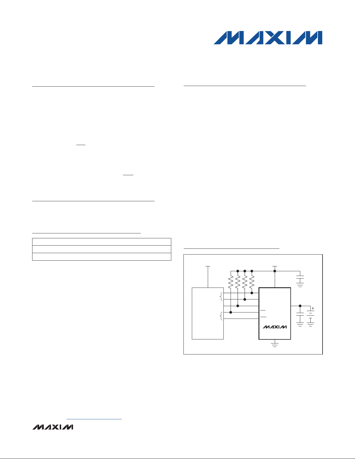
典型工作电路
+3.3V+3.3V
BAT
DS3231M
注意:该器件某些版本的规格可能与发布的规格不同,会以勘误表的形式给出。通过不同销售渠道可能同时获得器件的多个版本。欲了解器件勘误
表信息,请点击:
本文是英文数据资料的译文,文中可能存在翻译上的不准确或错误。如需进一步确认,请在您的设计中参考英文资料。
有关价格、供货及订购信息,请联络
或访问
Maxim
china.maxim-ic.com/errata
_______________________________________________________________ Maxim Integrated Products 1
的中文网站:
china.maxim-ic.com
。
Maxim
亚洲销售中心:
。
10800 852 1249 (
北中国区),
10800 152 1249 (
南中国区),
Page 2
5ppm、I2C
±
实时时钟
ABSOLUTE MAXIMUM RATINGS
Voltage Range on Any Pin Relative to GND ........-0.3V to +6.0V
Operating Temperature Range .......................... -40NC to +85NC
Storage Temperature Range ............................ -55NC to +125NC
Stresses beyond those listed under “Absolute Maximum Ratings” may cause permanent damage to the device. These are stress ratings only, and functional
operation of the device at these or any other conditions beyond those indicated in the operational sections of the specifications is not implied. Exposure to absolute
maximum rating conditions for extended periods may affect device reliability.
DS3231M
Lead Temperature (soldering, 10s) ................................+260NC
Soldering Temperature (reflow) ......................................+260NC
RECOMMENDED OPERATING CONDITIONS
(TA = -40NC to +85NC, unless otherwise noted.) (Note 1)
PARAMETER SYMBOL CONDITIONS MIN TYP MAX UNITS
Supply Voltage
Logic 1 V
Logic 0 V
V
V
BAT
CC
IH
IL
2.3 3.3 5.5
2.3 3.0 5.5
0.7 x
V
CC
-0.3
VCC +
0.3 x
V
0.3
CC
V
V
V
ELECTRICAL CHARACTERISTICS—FREQUENCY AND TIMEKEEPING
(VCC or V
T
= +25NC, unless otherwise noted.)
A
1Hz Frequency Tolerance
1Hz Frequency Stability vs. V
Voltage
Timekeeping Accuracy tK
32kHz Frequency Tolerance
= +3.3V, TA = -40NC to +85NC, unless otherwise noted. Typical values are at VCC = +3.3V, V
BAT
PARAMETER SYMBOL CONDITIONS MIN TYP MAX UNITS
Measured over R 10s interval Q5
OUT
A
OUT
CC
Df/f
Df/V Q1
Df/f
DC ELECTRICAL CHARACTERISTICS—GENERAL
(VCC = +2.3V to +5.5V, TA = -40NC to +85NC, unless otherwise noted. Typical values are at VCC = +3.3V, V
+25NC, unless otherwise noted.)
PARAMETER SYMBOL CONDITIONS MIN TYP MAX UNITS
Active Supply Current
(I2C Active: Includes
Temperature Conversion Current)
Standby Supply Current
2
(I
C Inactive: Includes
Temperature Conversion Current)
Temperature Conversion Current
2
C Inactive)
(I
I
CCA
I
CCS
I
CCSCONV
VCC = +3.63V 200
V
= V
CC
CCMAX
VCC = +3.63V 130
V
= V
CC
CCMAX
VCC = +3.63V 575
= V
V
CC
CCMAX
= +3.0V, and
BAT
Q0.432
= +3.0V, and TA =
BAT
Seconds/
Q2.5
300
200
650
ppm
ppm/V
Day
%
µA
µA
µA
2
Page 3
5ppm、I2C
±
DC ELECTRICAL CHARACTERISTICS—GENERAL (continued)
(VCC = +2.3V to +5.5V, TA = -40NC to +85NC, unless otherwise noted. Typical values are at VCC = +3.3V, V
+25NC, unless otherwise noted.)
PARAMETER SYMBOL CONDITIONS MIN TYP MAX UNITS
Power-Fail Voltage V
Logic 0 Output
(32KHZ, INT/SQW, SDA)
Logic 0 Output
(RST)
Output Leakage
(32KHZ, INT/SQW, SDA)
Input Leakage
(SCL)
RST I/O Leakage
Leakage I
V
BAT
Temperature Accuracy TEMP
Temperature Conversion Time t
Pushbutton Debounce PB
Reset Active Time t
Oscillator Stop Flag (OSF) Delay t
V
V
I
I
I
BATLKG
CONV
RST
OSF
PF
OL
OL
LO
LI
OL
ACCVCC
DB
IOL = 3mA 0.4 V
IOL = 1mA 0.4 V
or V
(Note 2) 125 200 ms
BAT
= +3.3V
2.45 2.575 2.70 V
-0.1 +0.1 µA
-0.1 +0.1 µA
-200 +10 µA
25 100 nA
10 ms
250 ms
250 ms
实时时钟
= +3.0V, and TA =
BAT
Q3 NC
DS3231M
DC ELECTRICAL CHARACTERISTICS—V
(VCC = 0V, V
and T
= +25NC, unless otherwise noted.)
A
Active Battery Current
2
(I
C Active) (Note 3)
Timekeeping Battery Current
2
(I
C Inactive) (Note 3)
Temperature Conversion Current
2
(I
C Inactive)
Data Retention Current
(Oscillator Stopped and I2C
Inactive)
= +2.3V to +5.5V, TA = -40NC to +85NC, unless otherwise noted. Typical values are at VCC = 0V, V
BAT
PARAMETER SYMBOL CONDITIONS MIN TYP MAX UNITS
V
= +3.63V 70
I
BATA
I
BATT
I
BATTC
I
BATDR
BAT
= V
V
BAT
V
BAT
V
BAT
V
BAT
V
BAT
TA = +25NC
BATMAX
= +3.63V, EN32KHZ = 0 2 3.0
= V
BATMAX
= +3.63V 575
= V
BATMAX
CURRENT CONSUMPTION
BAT
, EN32KHZ = 0 2 3.5
AC ELECTRICAL CHARACTERISTICS—POWER SWITCH
(TA = -40NC to +85NC, unless otherwise noted.) (Figure 2)
PARAMETER SYMBOL CONDITIONS MIN TYP MAX UNITS
V
Fall Time, V
CC
V
PFMIN
Rise Time, V
V
CC
V
PFMAX
Recovery at Power-Up t
PFMAX
PFMIN
to
to
t
VCCF
t
VCCR
REC
(Note 4) 250 300 ms
300
0
= +3.0V,
BAT
150
650
100 nA
µA
µA
µA
Fs
Fs
3
Page 4

5ppm、I2C
±
实时时钟
AC ELECTRICAL CHARACTERISTICS—I2C INTERFACE
(VCC or V
and T
SCL Clock Frequency f
Bus Free Time Between STOP
DS3231M
and START Conditions
Hold Time (Repeated) START
Condition
Low Period of SCL t
High Period of SCL t
Data Hold Time t
Data Set-Up Time t
START Set-Up Time t
SDA and SCL Rise Time t
SDA and SCL Fall Time t
STOP Set-Up Time t
SDA, SCL Input Capacitance C
Note 1: All voltages are referenced to ground.
Note 2: The parameter t
Note 3: Includes the temperature conversion current (averaged).
Note 4: This delay applies only if the oscillator is enabled. If the EOSC bit is 1, t
Note 5: Interface timing shown is for fast-mode (400kHz) operation. This device is also backward-compatible with standard mode
Note 6: C
= +2.3V to +5.5V, TA = -40NC to +85NC, unless otherwise noted. Typical values are at VCC = +3.3V, V
BAT
= +25NC, unless otherwise noted.) (Note 5, Figure 1)
A
PARAMETER SYMBOL CONDITIONS MIN TYP MAX UNITS
SCL
t
BUF
t
HD:STA
LOW
HIGH
HD:DAT
SU:DAT
SU:STA
R
SU:STO
BIN
is the period of time the oscillator must be stopped for the OSF flag to be set.
OSF
The state of RST does not affect the I2C interface or RTC functions.
I2C timing.
: Total capacitance of one bus line in picofarads.
B
(Note 6)
(Note 6)
F
is bypassed and RST immediately goes high.
REC
0 400 kHz
1.3
0.6
1.3
0.6
0 0.9
100 ns
0.6
20 +
0.1C
20 +
0.1C
0.6
B
B
10 pF
300 ns
300 ns
BAT
= +3.0V,
Fs
Fs
Fs
Fs
Fs
Fs
Fs
4
Page 5
SDA
t
BUF
t
LOW
SCL
t
HD:STA
STOP START REPEATED
NOTE: TIMING IS REFERENCED TO V
图
时序
1.I2C
ILMAX
AND V
IHMIN
t
R
t
HD:DAT
.
t
HIGH
t
F
t
SU:DAT
START
t
SU:STA
5ppm、I2C
±
t
HD:STA
实时时钟
t
SP
t
SU:STO
时序图
DS3231M
V
CC
RST
图
电源开关时序
2.
图
按钮复位时序
3.
V
PFMAX
V
PFMIN
t
VCCF
RST
t
VCCR
t
REC
PB
DB
t
RST
5
Page 6
5ppm、I2C
±
实时时钟
= +25°C, unless otherwise noted.)
(T
A
150
DS3231M
140
130
120
110
100
90
80
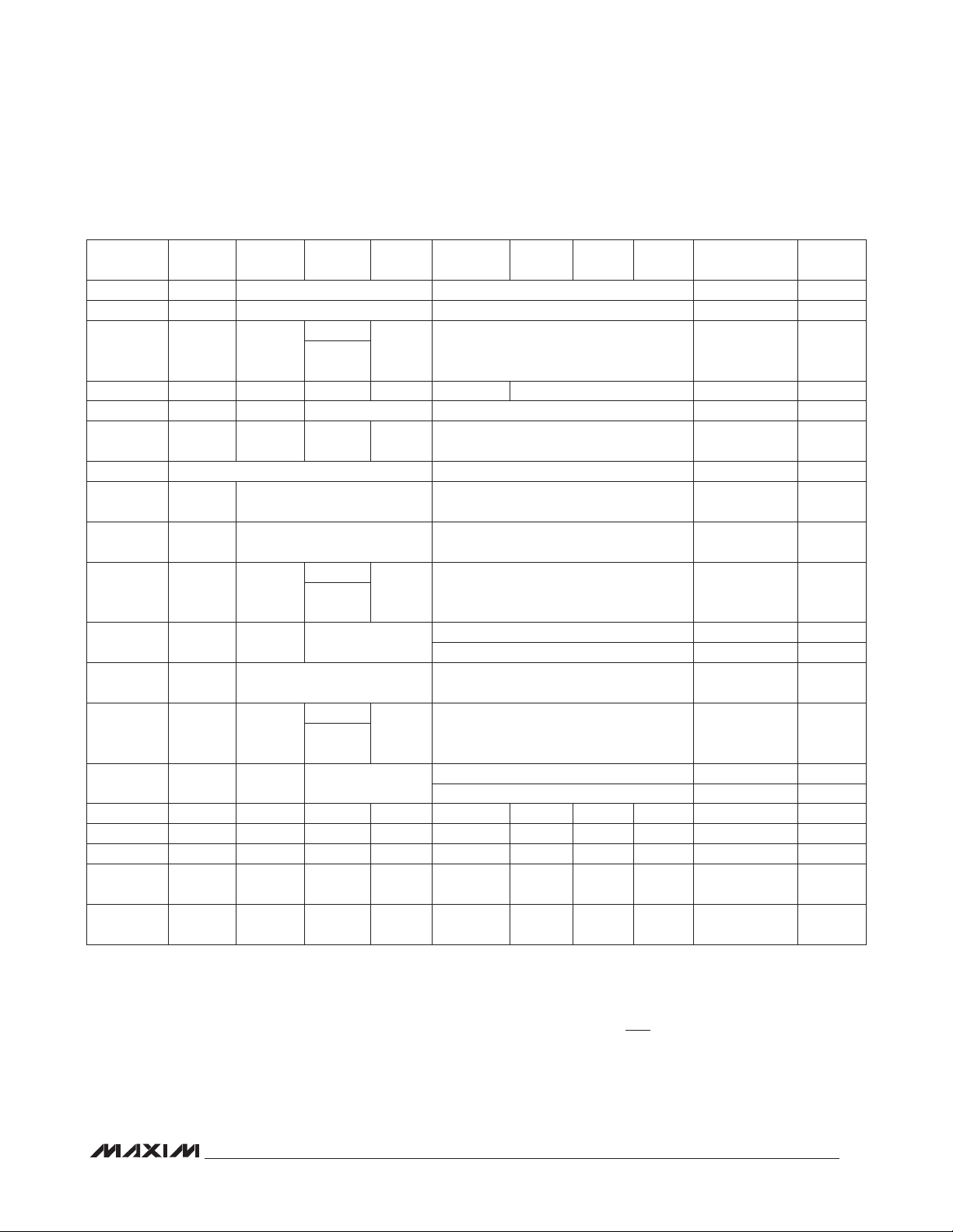
SUPPLY CURRENT (µA)
70
60
50
0.5
0.4
POWER-SUPPLY CURRENT
vs. POWER-SUPPLY VOLTAGE
V
= 2.3V, EN32KHZ = 1, I
BAT
+85°C
INCREASE BELOW V
DUE TO INTERNAL PULLUP
RESISTOR ON RST
2 6
SUPPLY VOLTAGE (V)
OUT
= 0mA
+25°C
-40°C
PF
543
INT/SQW OUTPUT VOLTAGE
vs. OUTPUT CURRENT
VCC = 2.3V,
= 0V,
V
BAT
= +25°C
T
A
DS3231M toc01
DS3231M toc03
BATTERY-SUPPLY CURRENT
vs. BATTERY-SUPPLY VOLTAGE
4.0
VCC = 0V, EN32KHZ = 1, BBSQW = 0
3.5
3.0
2.5
2.0
SUPPLY CURRENT (µA)
1.5
1.0
2 6
SUPPLY VOLTAGE (V)
+85°C
+25°C
-40°C
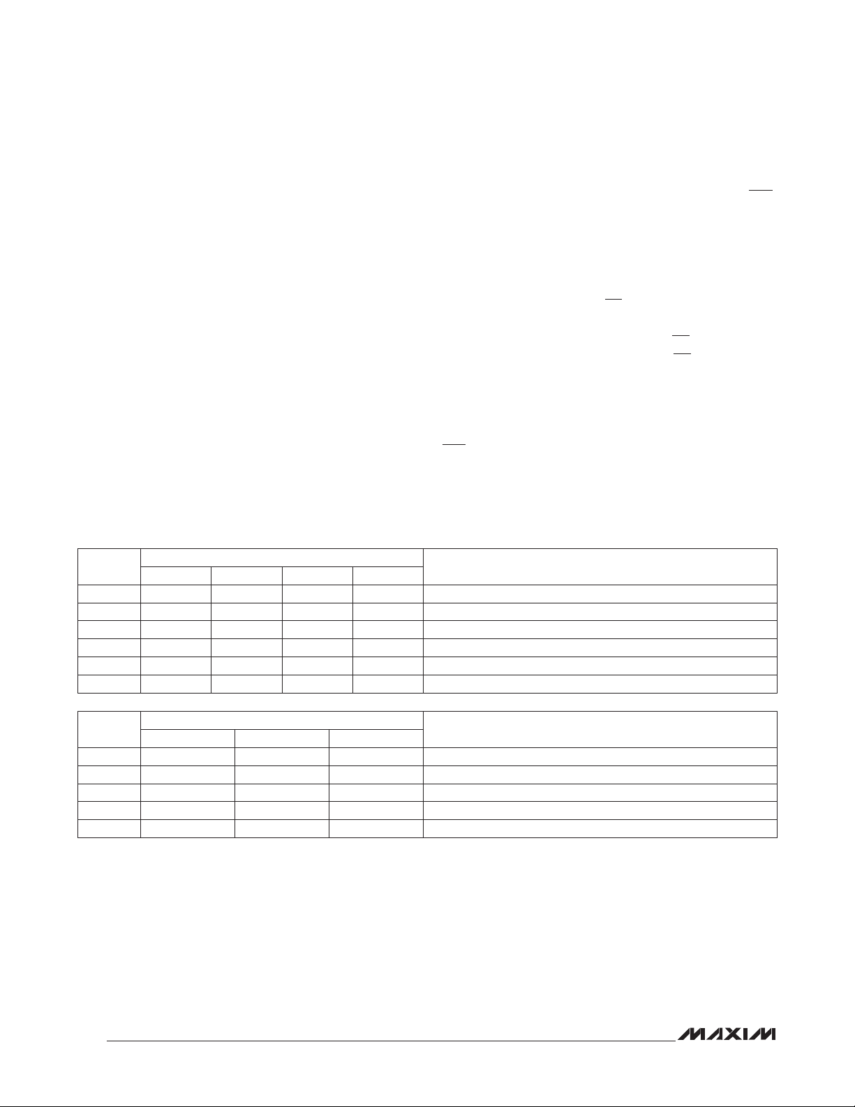
RST OUTPUT VOLTAGE
vs. OUTPUT CURRENT
0.5
VCC = 2.45V,
= 3.0V,
V
BAT
= +25°C
T
A
0.4
典型工作特性
DS3231M toc02
543
DS3231M toc04
0.3
0.2
OUTPUT VOLTAGE (V)
0.1
0
0 10
OUTPUT CURRENT (mA)
RST OUTPUT VOLTAGE
vs. POWER SUPPLY VOLTAGE
6
V
= 3.0V,
BAT
TA = +25°C
5
4
3
TRACKS WITH V
2
OUTPUT VOLTAGE (V)
1
0
0 6
SUPPLY VOLTAGE (V)
0.3
0.2
OUTPUT VOLTAGE (V)
0.1
8642
0
0 5
OUTPUT CURRENT (mA)
4321
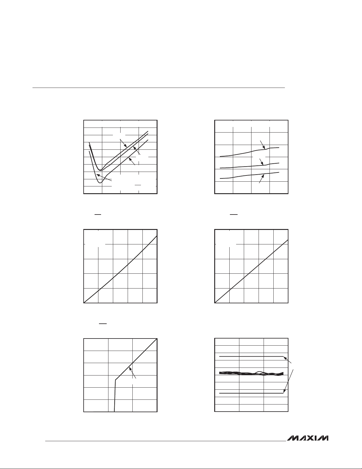
FREQUENCY ERROR
vs. TEMPERATURE
10
VCC = 3.3V
8
DS3231M toc05
CC
42
6
4
2
0
-2
-4
FREQUENCY ERROR (ppm)
-6
-8
-10
-50 100
TEMPERATURE (°C)
500
DS3231M toc06
LIMITS
6
Page 7

5ppm、I2C
±
实时时钟
DS3231M
TOP VIEW
引脚配置
引脚
8 SO 16 SO
1 1 32KHZ
2 2 V
3 3
32KHZ SCL
V
INT/SQW
RST
N.C.
N.C.
N.C.
N.C.
名称 功能
CC
INT/
SQW
+
1
2
CC
3
DS3231M
4
5
6
7
8
SO
32.768kHz输出(50%
EN32KHZ
用于主电源的直流电源引脚。该引脚应使用
低电平有效中断或
5.5V
定。当
时都会触发
为中断输出并禁止闹钟功能。
位使能后,可在任何一路电源供电时提供时钟输出。如不使用该引脚,可保持开路。
的电源电压。如不使用该引脚,可保持开路。该多功能引脚的功能由控制寄存器
INTCN
INT/SQW引脚(
16
SDA
15
V
14
BAT
13
GND
12
N.C.
11
N.C.
10
N.C.
9
N.C.
占空比)。该漏极开路输出引脚要求外接上拉电阻。通过状态寄存器
方波输出。该漏极开路输出引脚要求外接上拉电阻,上拉电阻连接到
1Hz
设定为0时,引脚输出
如果使能闹钟功能)。由于首次上电时
1Hz
TOP VIEW
INT/SQW
0.1μF至1.0μF
方波;当
32KHZ
CC
INTCN
+
1
2
DS3231M
3
4
SO
电容进行去耦。不用时,请接地。
87SCL
SDAV
V
6
GNDRST
5
BAT
引脚说明
中的
(0Fh)
5.5V
或低于
(0Eh)的INTCN
设定为1时,计时寄存器与任一闹钟寄存器相匹配
位设定为1,因此该引脚缺省设置
INTCN
位决
4 4
— 5–12 N.C.
5 13 GND
6 14 V
RST
BAT
低电平有效复位引脚。该引脚为漏极开路输入/输出。引脚指示
至低于
低电平有效、漏极开路输出还具有去抖按钮输入功能。该引脚可由按钮复位请求来触发。引脚内部通过
标称值为
RST
无连接。这些引脚必须接地。
地。
备用电源输入。器件将
件将
在使用锂电池时,可防止反向充电。更多信息请参考
,
V
立即进入高电平。
V
BAT
引脚被拉低。若
RST
PF
50kΩ(RPU)
输入用作备用电源时,无需使用电容。如果不使用
的上拉电阻连接至
输入用作主电源时,该引脚应使用
V
BAT
超过
V
CC
并持续
V
PF
,无需外接上拉电阻。如果禁止晶体振荡器,
V
CC
时间,
t
RST
china.maxim-ic.com/qa/info/ul
相对于
V
CC
引脚通过内部上拉电阻拉至高电平。
RST
0.1μF至1.0μF
,则将该引脚接地。器件经过UL认证,
V
BAT
指标的状态。如果
V
PF
t
REC
的低泄漏电容进行去耦。器
。
下降
V
CC
被屏蔽,
7
Page 8

5ppm、I2C
±
实时时钟
8 SO 16 SO
DS3231M
引脚
7 15 SDA
8 16 SCL
V
BAT
V
CC
RST
GND
名称 功能
N
串行数据输入
可高达
5.5V,与V
串行时钟输入。该引脚为
压无关。
DS3231M
R
PU
POWER
CONTROL
输出。该引脚为
/
电压无关。
CC
I2C
TIME-BASE
RESONATOR
TEMP
SENSOR
引脚说明(续
串口的数据输入/输出。此漏极开路引脚要求外接上拉电阻。上拉电压
I2C
串口的时钟输入,用于同步串口数据传输。上拉电压可高达
DIVIDER
DIGITAL
ADJUSTMENT
FACTORY TRIM
1Hz
INTERRUPT
OR 1Hz
SELECT
N
N
5.5V,与V
32KHZ
INT/SQW
CC
方框图
)
电
SDA
SCL
I2C
INTERFACE
DS3231M
电系统
在
-40°C至+85°C
秒/天之内。
闹钟。
方波。时钟/日历提供秒、分、时、星期、日期、月和年信息。
少于
8
串行 实 时时 钟
(MEMS)
INT/SQW
天的月份,将自动调整月末的日期,并包括闰年补偿。
31
驱动。振荡器提供稳定、精确的参考时钟,
温度范围内,
为低功耗时钟/日历,提供两个可编程日历
RTC
提供由闹钟条件决定的中断信号或者
由内 部 带 温 度补偿的 微 机
(RTC)
的精度保 持在
RTC
CONTROL AND STATUS
REGISTERS
详细说明
±
0.432
1Hz
CLOCK/CALENDAR
WITH ALARM
时钟可工作在24小时或带
寄存器通过
用于监视
至备用电源。
示电源故障。
总线接口访问。温补电压基准和比较器电路
I2C
电平,以检测电源故障,并在必要时自动切换
V
CC
引脚提供外部按钮输入功能,并可用于指
RST
AM/PM
指示的12小时格式。内部
方框图
给出了该器件的主要组成部分,在以下章节中将对每
个主要模块分别进行说明。
工作原理
Page 9

+3.3V
V
CC
5ppm、I2C
±
实时时钟
DS3231M
高精度时基
高精度时基由温度传感器、振荡器和数字调节控制逻辑电路
组成。控制器读取片内温度传感器的输出,通过调节最终的
输出以保持所要求的精度。器件在工厂经过校准,能够
1Hz
V
BAT
在整个工作温度范围内保持极高精度。采用
时,每秒钟进行一次校准。采用
秒钟进行一次校准,以节省电能。
这不会影响器件的长期计时精度。器件还具有一个老化补偿
寄存器,能够在工厂校准值上增加一个补偿常数
为器件供电时,每
V
BAT
时基无需频繁校准,
1Hz
为器件供电
V
CC
(
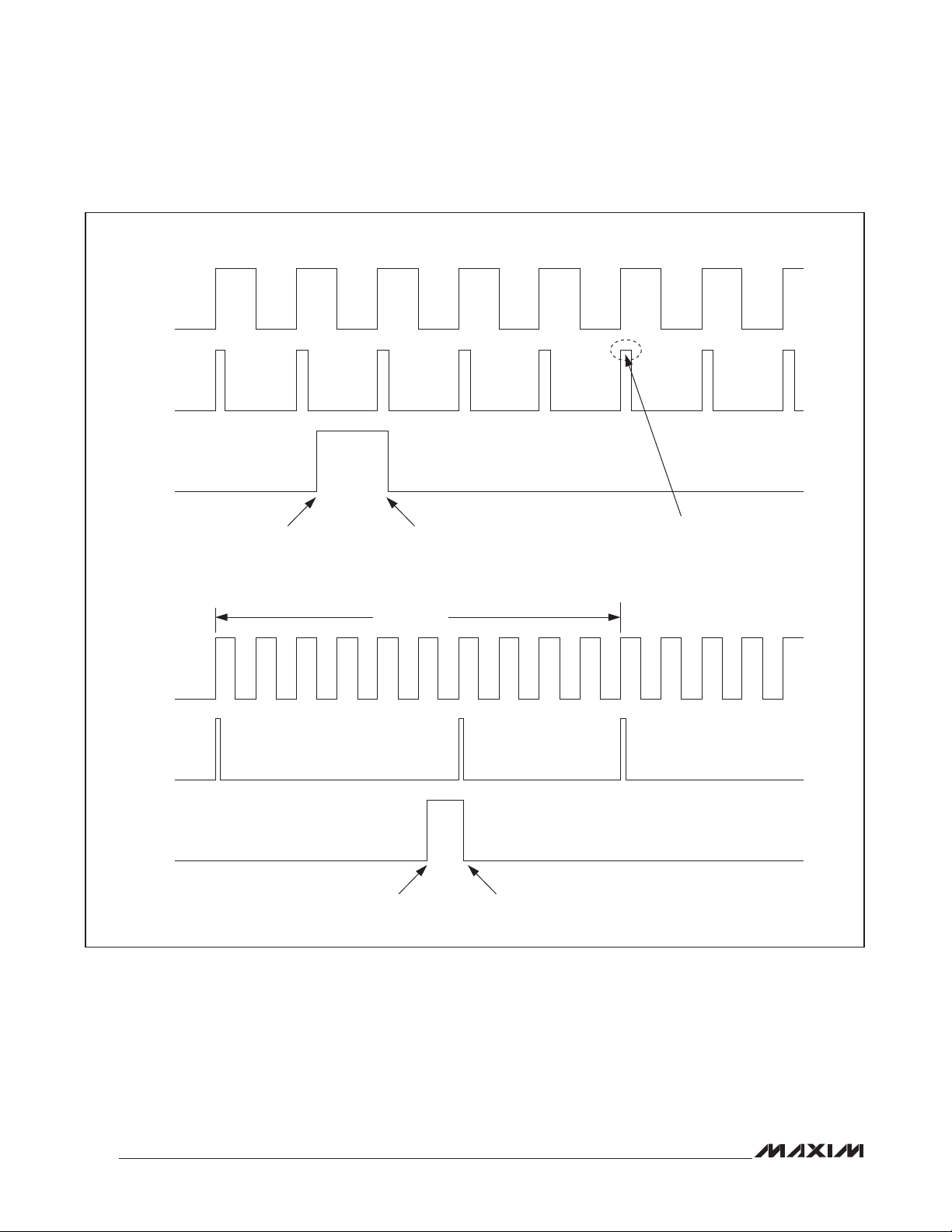
10
正或负)。
图
图
图
4.
5.
6.
单电源
单电源
双电源
(VCC)
(V
BAT
电源配置
DS3231M
电,双电源配置下提供一 个备用电源,在 未连接系统主电
V
CC
V
BAT
)
+3.3V
V
CC
V
BAT
源时保持计时电路正常工作。
图
4
地。当
执行一次温度转换。
图5所示为采用
地。
秒钟执行一次温度转换。
图
6
V
BAT
比较器电路监测
于
V
该器件由
V
BAT
当
VCC<V
作为电源时,每秒钟执行一次温度转换。当选择
电源时,每
为保护电池,
V
PF
不启动。典型的振 荡器启动时间在
或者有效的
可以配置为采用单电源
所示为采用
VCC<V
输出被禁止,并通过内部上拉电阻连接至地。每
RST
所 示 为双电 源配 置, 系 统 正常工作 时采 用
用作备用电源。该配置下,带温度补偿的电压基准和
时,器件由
PF
V
CC
供电(见表1)。
PF
10
以上 之前,或者向器件写入一个有效的
I2C
供电的单电 源配置,其中
V
CC
时,触发
PF
V
BAT
电压,并提供电源选择功能。当
V
CC
V
CC
供电。当
时,触发
秒钟执行一次温度转换。
首次加到 器 件上时 振 荡器在
V
BAT
地址写入后大约2秒钟,器件会测量一次温
RST输出(
供电的单电 源 配置,其中
供电。当
V
CC
低于
V
V
RST输出(
或
(V
CC
低电平有效)。每秒钟
V
BAT
或双电源供
)
V
BAT
V
CC
V
低于
CC
并低于
PF
低电平有效)。当选择
V
PF
V
但高于
时,器件由
BAT
V
地址 之前并
I2C
秒以内。在
1
V
CC
输入接
输入接
供电,
CC
V
V
BAT
BAT
V
CC
加电后
10
高
CC
时,
V
CC
作为
达到
表
电源控制
1.
CONFIGURATION CONDITION I/O ACTIVE I/O INACTIVE
V
V
Only
CC
(Figure 4)
V
Only
BAT
(Figure 5)
Dual Supply
(Figure 6)
> V
CC
< V
V
CC
EOSC = 0
EOSC = 1
V
> V
CC
V
< V
CC
PF
PF
PF
PF
VCC > V
< V
V
CC
BAT
BAT
I
CCA
I
BATA
I
CCA
I
CCA
I
BATA
VCC > V
VCC < V
BAT
BAT
I
CCS
I
BATT
I
BATDR
I
CCS
I
CCS
I
BATT
RST
Inactive (High)
Active (Low)
Disabled (Low)
Inactive (High)
Active (Low)
9
Page 10

5ppm、I2C
±
实时时钟
度,并 使用计算的 修正值校准振荡器。一旦振荡器运行起
来,只要电源
器件也将持续测量温度并校准振荡器 频率。
上电或向器件写入一个有效的
时间和日期寄存器被复位至
DD/YYDOWHH:MM:SS)
DS3231M
不同工作模式具有不同的
并且串口处于工作状态时,有效电池电流为
止时,电池电流为保持计时的电流
度转换电流
必须能够承受周期性的较大 脉冲电流,同时还需保 持有效
的电压值。数据保持电流
时的器件电流。在不必保留时间和日期信息时(例如最终产
品在等待运给客户时
器件提供连接至
件不在复位周期,会持续监视
到一个边沿转换,器件通过拉低
时器定时结束
依旧保持低电平,器件持续监视信号以检测上升沿。一旦检
测到按钮释放,器件强制
间。
RST
产生内部电源故障报警信号,并强制拉低
超过
以使供电电源稳定下来。如果在
将会跳过
I
还用来指示电源故障情况。当
电平时,
V
PF
t
REC
或者
(V
CC
。温度转换电流
)
BATTC
RST输入/
(PBDB)
RST
,
RST
有效就会一直保持运行状态,
V
)
BAT
电源首次
V
CC
地址时(如果
I2C
V
BAT
01/01/000100:00:00(MM/
。
V
电流。当器件采用
V
BAT
I
(
BATT
I
BATTC
I
,该模式可以降低对电池的要求。
)
后,器件继续监视
是振荡器停止
BATDR
输出引脚的按钮控制功能。若器
信号的下降沿。如果检测
RST
完成开关去抖。内部定
RST
RST
引脚为低电平 并 保持
RST
V
CC
RST
引脚保持低电平大约
加载时振荡器没有工作,
V
CC
立刻变为高电平。无论通过按钮或电源
V
。当串口禁
I
BATA
其中包括平均温
的定义源于系统
(EOSC=1)
按钮复位功能
信号。如果信号
低于
V
引脚。当
250ms(t
加电),
BAT
BAT
t
RST
时,会
PF
工作
供电
V
REC
时
CC
)
失效检测拉低
输出和手动复位监测功能仅在
采用带温度补偿的振荡器提供
时、星期、日期、月和年信息。少于
整月末日期,其中包括闰年的修正。时钟可工作在
带
AM/PM
钟。可以使能
者
1Hz
只要
果与该器件连接的微控制器由于
有可能造成微控制器与该器件的
控制器在从该器件读数据时发生复位。当微控制器复位时,
通过在
口置于已知状态。此时,微控制器应该在
SDA
表2给出了该器件计时寄存 器的地址映射表。在多字节访问
过程中,当地址指针到达寄存器空间的末尾
返回到地址
至地址
继续运行的同时,可从辅助寄存器中读取时间信息。这样在
读操作期间发 生 主寄存 器更 新 时, 可 以 避免 重 新 读取寄
,
存器。
指示的12小时格式。时钟提供两个可编程日历闹
方波信号,功能选择由控制寄存器中的
或
V
CC
SDA
拉低,产生一个
00h
输出,都不会影响器件的内部工作。
RST
供电时有效。
V
CC
实时时钟
信号时,
INT/SQW
1Hz
产生由闹钟条 件决定的中断信号或
RTC
天的月份,将自动调
31
INTCN
处于有效电压范围,即可访问
V
BAT
掉电或其它因素复位,
V
CC
通信不同步,例如 :微
I2C
达到高电平之前触发
,可以将器件的
SCL
SCL
START
条件。
(12h)
00h。在I2C的START
时,当前的时间会传输至辅助寄存器中。在时钟
条件下或者地址指针递增
RST
(RTC)
提供秒、分、
小时或
24
位控制。
接口
I2C
接口。如
I2C
接
I2C
为高电平时将
地址映射表
时,将会
10
Page 11
5ppm、I2C
±
表
计时寄存器
2.
ADDRESS
00h 0 10 Seconds Seconds Seconds 00–59
01h 0 10 Minutes Minutes Minutes 00–59
02h 0
03h 0 0 0 0 0 Day Day 1–7
04h 0 0 10 Date Date Date 01–31
05h Century 0 0
06h 10 Year Year Year 00–99
07h A1M1 10 Seconds Seconds
08h A1M2 10 Minutes Minutes
09h A1M3
0Ah A1M4
0Bh A2M2 10 Minutes Minutes
0Ch A2M3
0Dh A2M4
0Eh
0Fh OSF 0 0 0 EN32KHZ BSY A2F A1F Status —
10h SIGN DATA DATA DATA DATA DATA DATA DATA Aging Offset —
11h SIGN DATA DATA DATA DATA DATA DATA DATA
12h DATA DATA 0 0 0 0 0 0
注:除非另有说明,初次上电时的寄存器状态未做定义。
BIT 7
MSB
EOSC
BIT 6 BIT 5 BIT 4 BIT 3 BIT 2 BIT 1
AM/PM
12/24
12/24
DY/DT
12/24
DY/DT
BBSQW CONV NA NA INTCN A2IE A1IE Control —
20
Hours
AM/PM
20
Hours
10 Date
AM/PM
20
Hours
10 Date
10
Hours
10
Month
10
Hours
10
Hours
Hour Hours
Month Month/Century
Hour Alarm 1 Hours
Day Alarm 1 Day 1–7
Date Alarm 1 Date 1–31
Hour Alarm 2 Hours
Day Alarm 2 Day 1–7
Date Alarm 2 Date 1–31
BIT 0
LSB
实时时钟
FUNCTION RANGE
Alarm 1
Seconds
Alarm 1
Minutes
Alarm 2
Minutes
Temperature
MSB
Temperature
LSB
DS3231M
1–12 +
AM/PM
00–23
01–12 +
Century
00–59
00–59
1–12 +
AM/PM
00–23
00–59
1–12 +
AM/PM
00–23
—
—
时钟和日历
可以通过读取适当的寄存器字节获得时钟和日历信息。表
给出了
来设定或者初始化时钟和日历数据。时钟和日历寄存器的内
容采用二–十进制编码
寄存器的配置说明。通过写入适当的寄存器字节
RTC
格式。器件可以运行于12小时
(BCD)
或者24小时模式。小时寄存器的第6位定义为12小时或
小时模式选择位。该位 为高时,选择12小时模式。在12小
2
时模式下,第
小时模式下,第5位为20小时位
24
存器由
99
5
位为
AM/PM
指示位,逻辑高时为PM。在
(20至23小时)
溢出至00时,会转换世纪位(月寄存器的第7位)。
24
。当年寄
11
Page 12
5ppm、I2C
±
实时时钟
星期寄存器在午夜时递增。对应于星期的值由用户定义,但
是该值必须连续
依次类推
作。读取或写入时间和日期寄存器时,辅助缓存器用于防止
内部寄存器更新时可能出现的错误。读取时间和日期寄存器
时,辅助缓存器在任何
返回到零时与内部寄存器同步。时间信息从这些辅助寄存器
DS3231M
读取,此时时钟继续保 持 运行状态。这样在读操作期间发
生主寄存器更新时可以避免重新读取寄存器。任何时候写秒
寄存器时,倒计时链都会复位。在该器件应答后进行写传输
操作。一旦倒计时链复位,为避免翻转问题,必须在
之内写入剩余的时间和日期寄存器。
该器 件包含两个星期/日期闹钟。闹钟1可通 过 写入寄存 器
07h至0Ah
设定,参见表
表
闹钟屏蔽位
3.
DY/DT
X 1 1 1 1 Alarm once a second
X 1 1 1 0 Alarm when seconds match
X 1 1 0 0 Alarm when minutes and seconds match
X 1 0 0 0 Alarm when hours, minutes, and seconds match
0 0 0 0 0 Alarm when date, hours, minutes, and seconds match
1 0 0 0 0 Alarm when day, hours, minutes, and seconds match
即,如果1等于星期日,那么2等于星期一,
(
。不合逻辑的时间和日期输入会导致不确定的操
)
I2CSTART
来设定。闹钟2可通过写入寄存器
。可对闹钟进行 编程(通过 控制寄存 器的闹
2
ALARM 1 REGISTER MASK BITS (BIT 7)
A1M4 A1M3 A1M2 A1M1
条件下或者寄存器指针
0Bh至0Dh
秒钟
1
闹钟
来
钟使能位和
SQW
。当每个闹钟的屏蔽位均为逻辑0时,闹钟只有在计时寄
2)
存器中的值与存储于星期
时才会告警。闹钟也可以编程为每秒、分、时、星期或日期
重复告警。表
会导致不合逻辑的操作。
第
6位)
反映星期几还是月份中的日期。如果
钟将是与月份日期匹配的结果。如果
钟则是与星期几匹配的结果。当
的设 定值相匹配时,相应的闹钟标志位
辑
。如果对应的闹钟中断使能
1
辑1,并且
INT/SQW
匹配情况。
INTCN位)
输出。每个星期/日期闹钟寄存器的第7位是屏蔽位(表
给出了可能的设置。如 果不按照表中配 置,
3
用于控制存储于寄存 器第0位至第5位的闹钟值是
INTCN
信号。在时间和日期寄存器每秒更新时都会检测
,从而 在闹钟匹 配 条 件下触 发
日期闹钟寄存器的对应值相匹配
/
DY/DT位(
闹钟星期/日期寄存器的
设为逻辑0,闹
DY/DT
设为逻辑1,闹
DY/DT
寄存器值与闹钟寄存器
RTC
A1F或A2F
A1IE或A2IE
位设 定 为逻辑1时,闹 钟条 件 将 会触发
ALARM RATE
位也设定为逻
INT/
置为逻
DY/DT
X 1 1 1 Alarm once per minute (00 seconds of every minute)
X 1 1 0 Alarm when minutes match
X 1 0 0 Alarm when hours and minutes match
0 0 0 0 Alarm when date, hours, and minutes match
1 0 0 0 Alarm when day, hours, and minutes match
12
ALARM 2 REGISTER MASK BITS (BIT 7)
A2M4 A2M3 A2M2
ALARM RATE
Page 13
5ppm、I2C
±
BIT 7 BIT 6 BIT 5 BIT 4 BIT 3 BIT 2 BIT 1 BIT 0
EOSC
0 0 0 1 1 1 0 0
BBSQW CONV NA NA INTCN A2IE A1IE
控制寄存器
实时时钟
DS3231M
(0Eh)
BIT 7
BIT 6
BIT 5
BITS 4:3
BIT 2
BIT 1
BIT 0
使能振荡器。设定为逻辑
:
EOSC
电时,该位清零
止时,所有寄存器数据处于静态。
电池备份的方波使能。设定为逻辑
BBSQW
设定为逻辑0时,若
CONV
精度。器件执行温度补偿算法的速度无法达到每秒钟一次,由用户启动的温度转换不会影响内部更新周期。
从写入开始直到温度转换完成期间一直保持为
使用
NA
INTCN
若计时寄存器与任一个闹钟寄存器相匹配,则会触发
而与
A2IE
时)。当
A1IE
时)。当
:
转换温度。该位设定为
:
位。详细信息请参见图7。
CONV
不适用。这些位不影响器件工作,可以设置为
:
中断控制。该位控制
:
位的状态无关。初次上电时,
INTCN
闹钟
中断使能。该位设定为逻辑1时,允许状态寄存器中的闹钟2标志位
2
:
位设定为0或者
A2IE
闹钟
中断使能。该位设定为逻辑1时,允许状态寄存器中的闹钟1标志位
1
:
位设定为0或者
A1IE
(逻辑0)
V
CC
。当该器件由
降至
时,启动振荡器。设定为逻辑1时,在器件电源切换至
0
供电时,振荡器与
V
CC
,并且当
以下,则
V
PF
1
INT/SQW
时,强制温度传感器将温度转换成数字码,并执行温度补偿算法以更新振荡器的
1
1
INT/SQW
输出信号。
INTCN=0、VCC<V
引脚变为高阻态。初次上电时,该位被禁止(逻辑0)。
,转换完后
。
0或1
设定为0时,
INTCN
INT/SQW输出(
位设定为逻辑1。
INTCN
位的状态无关,始终保持运行状态。当振荡器被禁
EOSC
时,该位使能
PF
CONV和BSY
均变为0。在监视用户启动转换的状态时应该
INT/SQW
如果也使能闹钟的话)。相应的闹钟标志总是置位,
引脚输出
时振荡器停止。初次上
V
BAT
方波输出。当
1Hz
方波。
1Hz
INTCN
(A2F)触发INT/SQW信号(当INTCN=1
INTCN
设定为0时,
位不启动中断信号。初次上电时,
A2F
位被禁止(逻辑0)。
A2IE
(A1F)触发INT/SQW信号(当INTCN=1
INTCN
设定为0时,
位不启动中断信号。初次上电时,
A1F
位被禁止(逻辑0)。
A1IE
设定为1时,
BBSQW
CONV
位
13
Page 14
5ppm、I2C
±
INTERNAL 1Hz
DS3231M
BSY
CONV
实时时钟
VCC POWERED
CLOCK
图
7.CONV
V
BAT
INTERNAL 1Hz
CLOCK
BSY
CONV
控制位和
THE USER SETS THE CONV BIT
POWERED
状态位的工作情况
BSY
THE DEVICE CLEARS THE CONV BIT
AFTER THE TEMPERATURE CONVERSION
10 SECONDS
THE USER SETS THE CONV BIT
BSY IS HIGH DURING
THE TEMPERATURE CONVERSION
HAS COMPLETED
THE DEVICE CLEARS THE CONV BIT
AFTER THE TEMPERATURE CONVERSION
HAS COMPLETED
14
Page 15

5ppm、I2C
±
BIT 7 BIT 6 BIT 5 BIT 4 BIT 3 BIT 2 BIT 1 BIT 0
OSF 0 0 0 EN32KHZ BSY A2F A1F
1 0 0 0 1 X X X
实时时钟
状态寄存器
DS3231M
(0Fh)
振荡器停止标志。该位为逻辑
:
OSF
无论何时振荡器停止工作,该位均置为逻辑
初次上电。
BIT 7
BITS 6:4
BIT 3
BIT 2
BIT 1
BIT 0
1)
与
2)V
CC
在电池备份模式下,
3)
影响振荡器的外部因素(即噪声、泄漏等)。
4)
未使用
EN32KHZ
化上电时,该位为逻辑
:
BSY
换后,该位清零。详细信息请参见
:
A2F
逻辑
1
:
A1F
,则触发
辑
1
上的电压都不足以支持振荡器工作。
V
BAT
。这些位没有意义,读操作时固定为0。
(0)
使能
32.768kHz
:
忙。该位表示器件正在执行温度转换功能。温度传感器的转换控制信号使该位置为逻辑
闹钟
标志。闹钟2标志位为逻辑1时表示时间与闹钟2寄存器匹配。如果
2
,则触发
闹钟
INT/SQW
标志。闹钟1标志位为逻辑1时表示时间与闹钟1寄存器匹配。如果
1
INT/SQW
位关闭。
EOSC
输出。该位控制
,使能
1
引脚。写入逻辑0时
引脚。写入逻辑0时
BIT 7 BIT 6 BIT 5 BIT 4 BIT 3 BIT 2 BIT 1 BIT 0
SIGN DATA DATA DATA DATA DATA DATA DATA
0 0 0 0 0 0 0 0
表示振荡器现在停止工作,或者曾经停止工作,可用于判定计时数据的有效性。
1
32KHZ
方框图
。该位保持为逻辑1,直到写入逻辑0清除。以下情况能够造成
1
输出,如果振荡器使能,则产生
。
位清零。该位仅能写入逻辑0,试图写入逻辑1的操作不改变原逻辑值。
A2F
位清零。该位仅能写入逻辑0,试图写入逻辑1的操作不改变原逻辑值。
A1F
32.768kHz
方波信号。
位为逻辑1,并且
A2IE
位为逻辑1,并且
A1IE
输出的使能和禁止。设定为逻辑0时,
32KHZ
输出变为高阻态。初始
32KHZ
;当器件完成温度转
1
老化补偿寄存器
INTCN
INTCN
置位:
OSF
位设定为
位设定为逻
(10h)
老化补偿寄存器用于在工厂设定的时基校准值上增加或减去一个用户提供的数值。如果只是要求达到
则不需要使用老化补偿寄存器。
老化补偿值采用
频率变化
(ppm)
的补码形式,第7位为符号
2
相同。正补偿值会减慢时基,而负补偿值会加快时基。
(SIGN)
位。一个
通常对应于
LSB
0.12ppm
的频率变化。在整个工作温度范围内,每个
ElectricalCharacteristics
表中规定的精度,
对应的
LSB
15
Page 16

5ppm、I2C
±
实时时钟
温度寄存器(高字节
BIT 7 BIT 6 BIT 5 BIT 4 BIT 3 BIT 2 BIT 1 BIT 0
SIGN DATA DATA DATA DATA DATA DATA DATA
DS3231M
0 0 0 0 0 0 0 0
温度寄存器
BIT 7 BIT 6 BIT 5 BIT 4 BIT 3 BIT 2 BIT 1 BIT 0
DATA DATA 0 0 0 0 0 0
0 0 0 0 0 0 0 0
温度 值 采用10位编 码表示,具有
低2位(小数部分)位于地址
在
初次上电或
V
CC
用户启动的转换结束后都会更新温度寄存器,温度寄存器是只读的。
器件的从地址字节为
件识别位、器件地 址和
地址必须与分配给器件的地址相匹配。
下列术语常用于
主机器件:主机器件用于控制总线上的从机器件。主机
器件产生
从机器件:从机器件按照主机请求发送、接收数据。
= 11h)
低字节
(
= 12h)
。例如,
12h
供电下首次进行
V
BAT
。发送到器件的第一个字节包括器
D0h
R/W位(图8)。I2C
数据传输的说明。
I2C
时钟脉冲以及
SCL
MSB
1 1 10 R/W000
DEVICE
IDENTIFIER
的分辨率,访问地 址为
0.25°C
0001100101b=+25.25°C
通信时,开始读取温度值,之后每秒(采用
I2C
串口工作原理
I2C
I2C
主机 发 送的器件
START和STOP
LSB
READ/
WRITE BIT
从地址
I2C
条件。
定义
11h和12h
。温度编码为2的补码格 式。高8位(整数部分)位于地址
。上电复位后,寄存器的缺省温度值设定为
供电
V
总线空闲或不忙:在
和
SCL
从器件通常启动低功耗模式。
START
机之间的数据传输。
电平到低电平的跳变将产生一个
序如图
STOP
数据传输。
平的跳变将产生一个
重复
START
采用重复
动一次新的数据传输。读操作期间,重复
通常表示对一 个特定存储地址启动一次数据传输。重
复
START
际时序如图
)或每10秒(采用V
CC
STOP和START
都无效且处于逻辑高电平状态。当总线空闲时,
条件:主机产生
SCL
所示。
1
条件:主机产生
保持高电平期间,
SCL
STOP
条件:在一次数据传输结束后,主机可以
START
条件指示在当前数据传输后将立即启
条件的产生方式与普通
所示。
1
温度寄存器
0°C
BAT
START
STOP
条件启动一次新的与从
保持高电平期间,
条件以终止与从机之间的
条件,实际时序如图1所示。
(11h至12h)
,控制器启动温度转换。
读取一次。每次由
供电
)
条件之间,
SDA
START
条件,实际时
由低电平到高电
SDA
START
START
条件相同,实
11h
SDA
由高
条件
,
图
16
8.I2C
从机地址字节
Page 17

5ppm、I2C
±
实时时钟
写位:
个
SCL
(见图1),SDA
上升沿,数据移入器件。
读位:写操作结束后,主机应在读位期间释放
并在
图
1)
据通过
据位有效。注意,由主机产生所有
从机读取数据位的时钟。
应答
常在字节传输的第
期间的主机 或写操作期间的从机
进行
ACK和NACK
答器件已经收到的数据,
示器件没有收到数据。
写字节:写字节操作包括
高有效位在前
照写位定义完成
应答。
读字节:读字节操作包括从机向主机发送的8位信息和
主机发送给从机的
义读取从机向主机发送的
主机按照写位定义发送
节。主机应在读取最后一个字节后发 送
通信,使从机将
从机地址字节:
后发送的从机地址字节进行响应。从机地址字节包含
位高有效位从机地址和最 低有效位
机地址为
的跳变只能发生在
SDA
脉冲为高电平以及所要求的建立、保持时间内
上的数据必须保持有效且不变。在
的低电平期间。在整
SCL
SDA
的下一个上升沿之前保持适当的建立时间(见
SCL
。在前一个
移出,并在当前
SDA
(ACK和NACK)
。器件在第9位期间发送1,以
ACK
脉冲的下降沿,器件将 每一位数
SCL
脉冲的上升沿保持数
SCL
时钟,包括从
SCL
:应答
位发送。接收数据的器件(读操作
9
或非应答
(ACK)
在第9位期间发送
)
(NACK)
NACK
的时序与其它位的写操作相同。
用于终止读过程或表
NACK
主机传送到从机的8位信息(最
和从机发送给主机的1位应答。主机按
)
位数据的发送,按照读位定义读 取
8
1位ACK或NACK
位信息(最高有效位在前),
8
,以继续接收其它数据字
ACK
。主机按照读位定
ACK
NACK
的控制权交还给主机。
SDA
总线的每个从机将对
I2C
,用户不能修改该地址。
D0h
START
位。器件的从
R/W
R/W=0时(
SCL
总线,
通
响应。
应
,终止
条件之
为
,表示主 机将向从机 写入数据。
D0h)
,主机将从 从机读取数据。如果写入错误的从机
D1h)
地址,器件将判定主机与其它
次发送
START
存储器地址:
址以确定 从机存储数据的位置。写操作期间,存储器
地址始终为从机地址字节之后发送的第二个字节。
时序举例请参见图9。
I2C
向从机写入单个字节:主机必须产生
机地址字节
产生
0
STOP
间读取从机发送的应答位。
向从机写入多个字节:为了向从机写入多个字节,主机
应产生
存储器地址、写入多个数据字节并产生
从从机读取单个字节:与写操作中利用指定的存储器地
址字节定义数据写入的位置不同,读操作地址对应于
存储器地址计数器的当前位置。为了从从机读取单个字
节,主 机 发送
然后读取数据字节并以
生
STOP
储器地址计数器,因此使用该方法在读操作时修改地
址计数器。
读操作时的地址计数器修改:可以采用空写操作将地
址计数器指向一个特定值。为此,主机可以产生一个
START
7
读取数据的存储器地址, 产生一次重复
写从机地址字节
读取的数据,最后发送
条件指定起始存储器位置的读操作示例,请参见图6。
条件之前忽略通信操作。
写操作期间,主机必须发送存储器地
I2C
(R/W=0)
条件。注意,主机必须在整个字节写操作期
START
条件、写从机地址字节
START
条件。由于实际应用中,无法要求主机跟踪存
条件,写从机地址字节
、写存储器地址、写数据字节并
条件,写从机地 址
(R/W=1)
I2C
指示终止传输,然后产
NACK
(R/W=0)
,并以
条件。采用重复
STOP
R/W=1时(
器件通信,并在下一
条件、写从
START
(R/W=0)
STOP
(R/W=1)
,写入需要
START
ACK或NACK
通信
I2C
、写
条件。
条件,
响应
START
为
,
DS3231M
17
Page 18

5ppm、I2C
±
2
C WRITE TRANSACTION
TYPICAL I
MSB LSB MSB LSB MSB LSB
START
1 1 0 1 0 0 0
实时时钟
SLAVE
R/W
ACK
b7 b6 b5 b4 b3 b2 b1 b0
SLAVE
b7 b6 b5 b4 b3 b2 b1 b0
ACK
SLAVE
ACK
STOP
READ/
WRITE
D0h 0Eh
1 1 0 1 0 0 0 0 0 0 0 0 1 1 1 0
SLAVE
ACK
D0h
SLAVE
ACK
D0h 04h
SLAVE
ACK
D0h 0Ch
SLAVE
ACK
0Eh
DS3231M
EXAMPLE I
A)
B)
C)
D)
图
9.I2C
2
C TRANSACTIONS
SINGLE BYTE WRITE
-WRITE CONTROL REGISTER
TO 44h
SINGLE BYTE READ
-READ CONTROL REGISTER
MULTIBYTE WRITE
-WRITE DATE REGISTER
TO "02" AND MONTH
REGISTER TO "11"
MULTIBYTE READ
-READ ALARM 2 HOURS
AND DATE VALUES
传输
SLAVE
ADDRESS
START
START
START 1 1 0 1 0 0 0 0 0 0 0 0 0 1 0 0
START 1 1 0 1 0 0 0 0 0 0 0 0 1 1 0 0
从从机读取多个字节:可以通过读操作在一次数据传
输过程中读取多个字节。从从机读取多个字节时,主机
在终止传输之前,如果需要继续读取另一个字节,只
需简单地发出
个字节后,必须发出
条件。
STOP
以应答数据字节。主机读取最后一
ACK
指示 终止传输,然后产生
NACK
应用信息
电源去耦
使用
DS3231M
电容对
1.0μF
质量的表贴陶瓷电容。表贴元件可减小引线电感、提高性能,
陶瓷电容具有较好的高频响应,适用于去耦应用。
如果在电 池 供电期间无 需 进 行 通信,可以省去
电容。
时,为获得最佳工作性能,采用
和
V
/或V
CC
电源进行去耦。尽可能采用高
BAT
0.1μF和/
V
BAT
REGISTER ADDRESS
SLAVE
0 1 0 0 0 1 0 0
ACK
SLAVE
ACK
SLAVE
0 0 0 0 0 0 1 0
ACK
SLAVE
ACK
或
去耦
DATA
44h
SLAVE
STOP
ACK
REPEATED
START
02h
REPEATED
START
D1h
1 1 0 1 0 0 0 1
SLAVE
ACK
D1h
1 1 0 1 0 0 0 1 VALUE
32KHZ和INT/SQW
SLAVE
ACK
0 0 0 1 0 0 0 1
SLAVE
ACK
DATA
VALUE
11h
DATA
SLAVE
ACK
MASTER
NACK
STOP
MASTER
ACK
为漏极开路输出,因此需要外接上拉电
阻,以 实现逻辑高电平。上拉电阻值通常在
之间。
也为漏极开路输出,但引脚内部提供了上拉 至
RST
50k
Ω
电阻
,无需外接上拉电阻。
(RPU)
SDA和SCL
为漏极开路输出,需要外接上拉电阻,以实现逻辑高
SDA
电平。
由于器件不使用时钟扩展功能,因此
开路 输出
带上拉电阻)或
(
CMOS
主机。
器件具有
的冗余电池充电保护电路,可防止对任何
Maxim
外部电池充电。
SCL
输出驱动器(推挽 输出)的
STOP1 1 0 1 0 0 0 0 0 0 0 0 1 1 1 0
DATA
MASTER
NACK
使用漏极开路输出
至
1k
Ω
上拉电阻
可以连接具有漏极
电池充电保护
STOPVALUE
10M
V
CC
Ω
的
18
Page 19

如需最近的封装外形信息和焊盘布局,请查询
封装图中可能包含不同的尾缀字符,但封装图只与封装有关,与
封装类型 封装编码 外形编号 焊盘布局编号
16 SO W16+2
8 SO S8+4
china.maxim-ic.co m/packages
RoHS
状态无关。
5ppm、I2C
±
实时时钟
。请注意,封装编码中的“+”、“#”或“-”仅表示
21-0042 90-0107
21-0041 90-0096
封装信息
状态。
RoHS
DS3231M
19
Page 20

5ppm、I2C
±
实时时钟
修订号 修订日期 说明 修改页
0 6/10
最初版本。
DS3231M
修订历史
—
Maxim
北京
免费电话:
电话:
传真:
Maxim不对Maxim
20 Maxim Integrated Products, 120 San Gabriel Drive, Sunnyvale, CA 94086 408-737-7600
©
2010MaximIntegratedProducts Maxim是MaximIntegratedProducts,Inc.
北京办事处
8328信箱
010-6211 5199
010-6211 5299
邮政编码
800 810 0310
100083
产品以外的任何电路使用负责,也不提供其专利许可。
保留在任何时间、没有任何通报的前提下修改产品资料和规格的权利。
Maxim
的注册商标。
 Loading...