

Page 1
www.maxim-ic.com
DS3171/DS3172/DS3173/DS3174
Single/Dual/Triple/Quad
DS3/E3 Single-Chip Transceivers
GENERAL DESCRIPTION
The DS3171, DS3172, DS3173, and DS3174
(DS317x) combine a DS3/E3 framer(s) and LIU(s) to
interface to as many as four DS3/E3 physical copper
lines.
APPLICATIONS
Access Concentrators Multiservice Access
SONET/SDH ADM
and Muxes
PBXs
Digital Cross Connect
Test Equipment
Platform (MSAP)
Multiservice Protocol
Platform (MSPP)
PDH Multiplexer/
Demultiplexer
Routers and Switches Integrated Access Device
(IAD)
ORDERING INFORMATION
PART TEMP RANGE PIN-PACKAGE
DS3171
DS3171N -40°C to +85°C
DS3172
DS3172N -40°C to +85°C
DS3173
DS3173N -40°C to +85°C
DS3174
DS3174N -40°C to +85°C
Note: Add the “+” suffix for the lead-free package option.
0°C to +70°C
0°C to +70°C
0°C to +70°C
0°C to +70°C
400 TE-PBGA (27mm x
27mm, 1.27mm pitch)
400 TE-PBGA (27mm x
27mm, 1.27mm pitch)
400 TE-PBGA (27mm x
27mm, 1.27mm pitch)
400 TE-PBGA (27mm x
27mm, 1.27mm pitch)
400 TE-PBGA (27mm x
27mm, 1.27mm pitch)
400 TE-PBGA (27mm x
27mm, 1.27mm pitch)
400 TE-PBGA (27mm x
27mm, 1.27mm pitch)
400 TE-PBGA (27mm x
27mm, 1.27mm pitch)
FUNCTIONAL DIAGRAM
DS3/E3
PORTS
DS3/
E3
LIU
DS3/E3
FRAMER/
FORMATTER
DS317x
SYSTEM
BACKPLANE
FEATURES
Single (DS3171), Dual (DS3172), Triple
(DS3173), or Quad (DS3174) Single-Chip
Transceiver for DS3 and E3
All Four Devices are Pin Compatible for Ease of
Port Density Migration in the Same Printed
Circuit Board Platform
Each Port Independently Configurable
Performs Receive Clock/Data Recovery and
Transmit Waveshaping for DS3 and E3
Jitter Attenuator can be Placed Either in the
Receive or Transmit Paths
Interfaces to 75Ω Coaxial Cable at Lengths Up to
380 meters, or 1246 feet (DS3) or 440 meters, or
1443 feet (E3)
Uses 1:2 Transformers on Both Tx and Rx
On-Chip DS3 (M23 or C-Bit) and E3 (G.751 or
G.832) Framer(s)
Ports Independently Configurable for DS3, E3
Built-In HDLC Controllers with 256-Byte FIFOs
for the Insertion/Extraction of DS3 PMDL, G.751
Sn Bit, and G.832 NR/GC Bytes
On-Chip BERTs for PRBS and Repetitive Pattern
Generation, Detection, and Analysis
Large Performance-Monitoring Counters for
Accumulation Intervals of at Least 1 Second
Flexible Overhead Insertion/Extraction Ports for
DS3, E3 Framers
Note: Some revisions of this device may incorporate deviations from published specifications known as errata. Multiple revisions of any device
may be simultaneously available through various sales channels. For information about device errata, click here: www.maxim-ic.com/errata
1
REV: 110206
.
Page 2

DS3171/DS3172/DS3173/DS3174
FEATURES (CONTINUED)
Loopbacks Include Line, Diagnostic, Framer,
Payload, and Analog with Capabilities to Insert
AIS in the Directions Away from Loopback
Directions
Ports can be Disabled to Reduce Power
Integrated Clock Rate Adapter to Generate the
Remaining Internally Required 44.736MHz (DS3)
and 34.368MHz (E3) from a Single Clock
Reference Source at One of Three Standard
Frequencies (DS3, E3, STS-1)
Pin Compatible with the DS318x Family of
Devices and the DS316x Family of Devices
8-/16-Bit Generic Microprocessor Interface
Low-Power (~1.73W) 3.3V Operation (5V
Tolerant I/O)
Small High-Density Thermally Enhanced Plastic
BGA Packaging (TE-PBGA) with 1.27mm Pitch
Industrial Temperature Operation:
-40°C to +85°C
IEEE1149.1 JTAG Test Port
DETAILED DESCRIPTION
The DS3171 (single), DS3172 (dual), DS3173 (triple), and DS3174 (quad) perform framing, formatting, and line
transmission and reception. These devices contain integrated LIU(s), framer/formatter for M23 DS3, C-bit DS3,
G.751 E3, G.832 E3, or a combination of the above signal formats.
Each LIU has independent receive and transmit paths. The receiver LIU block performs clock and data recovery
from a B3ZS- or HDB3-coded AMI signal and monitors for loss of the incoming signal, or can be bypassed for
direct clock and data inputs. The receiver LIU block optionally performs B3ZS/HDB3 decoding. The transmitter LIU
drives standard pulse-shape waveforms onto 75Ω coaxial cable or can be bypassed for direct clock and data
outputs. The jitter attenuator can be placed in either transmit or receive data path when the LIU is enabled. The
DS3/E3 framers transmit and receive serial data in properly formatted M23 DS3, C-bit DS3, G.751 E3, or G.832 E3
data streams. Unused functions can be powered down to reduce device power. The DS317x DS3/E3 SCTs
conform to the telecommunications standards listed in Section 4
.
2
Page 3
DS3171/DS3172/DS3173/DS3174
Ω
Ω
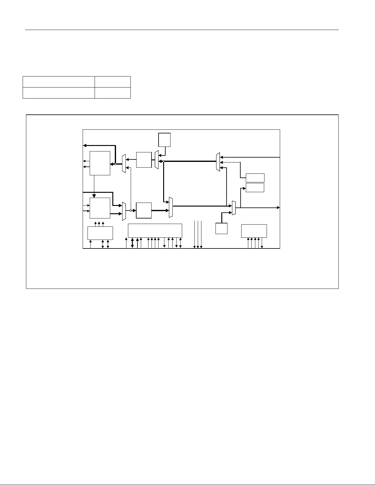
1 BLOCK DIAGRAMS
Figure 1-1 shows the external components required at each LIU interface for proper operation. Figure 1-2 shows
the functional block diagram of one channel DS3/E3 LIU.
Figure 1-1. LIU External Connections for a DS3/E3 Port of a DS317x Device
Transmit
Each DS3/E3 LIU Interface
TXP
330
(1%)
TXN
1:2ct
Receive
RXP
330
(1%)
RXN
1:2ct
Figure 1-2. DS317x Functional Block Diagram
VDD
VDD
VDD
VSS
VSS
VSS
0.01uF
0.01uF
0.01uF
0.1uF
0.1uF
0.1uF
1uF
1uF
1uF
Ground
Plane
3.3V
Power
Plane
TOHCLKn
TOHSOFn
TOHn
TCLKOn/TGCLKn
TSOFOn/TDENn
TOHENn
TAIS
TPOSn/
RNEGn/
TDATn
TNEGn
TLCLKn
TXPn
TXNn
RDATn
RLCVn
RLCLKn
RXPn
RXNn
DS3/E3
Transmit
LIU
ALB
DS3/E3
Receive
LIU
Clock Rate
Adapter
CLKB
CLKA
CLKC
RST
B3ZS/
HDB3
Encoder
LLB
B3ZS/
HDB3
Decoder
A[10:1]
D[15:0]
TUA1
DLB
Microprocessor
Interface
CS
ALE
RD/DS
WR/ R/W
A[0]/BSWAP
RDY
MODE
FEAC
INT
WIDTH
DS3 / E3
Transmit
Formatter
Trail
Trace
Buffer
DS3 / E3
Receive
Framer
GPIO[8:1]
ROHn
ROHCLKn
ROHSOFn
HDLC
UA1
GEN
DS317x
PLB
TX BERT
RX BERT
IEEE P1149.1
JTAG Test
Access Port
JTMS
JTRST
JTCLK
JTDI
JTDO
TCLKIn
TSERn
TSOFIn
RSERn
RCLKOn/RGCLKn
RSOFOn/RDENn
n = port # (1-4)
3
Page 4

DS3171/DS3172/DS3173/DS3174
TABLE OF CONTENTS
1 BLOCK DIAGRAMS 3
2 APPLICATIONS 12
3 FEATURE DETAILS 13
3.1 GLOBAL FEATURES........................................................................................................................................ 13
3.2 RECEIVE DS3/E3 LIU FEATURES .................................................................................................................. 13
3.3 RECEIVE DS3/E3 FRAMER FEATURES............................................................................................................ 13
3.4 TRANSMIT DS3/E3 FORMATTER FEATURES.................................................................................................... 13
3.5 TRANSMIT DS3/E3 LIU FEATURES ................................................................................................................ 14
3.6 JITTER ATTENUATOR FEATURES..................................................................................................................... 14
3.7 CLOCK RATE ADAPTER FEATURES ................................................................................................................. 14
3.8 HDLC OVERHEAD CONTROLLER FEATURES ................................................................................................... 14
3.9 FEAC CONTROLLER FEATURES..................................................................................................................... 14
3.10 TRAIL TRACE BUFFER FEATURES ................................................................................................................... 15
3.11 BIT ERROR RATE TESTER (BERT) FEATURES ................................................................................................15
3.12 LOOPBACK FEATURES ................................................................................................................................... 15
3.13 MICROPROCESSOR INTERFACE FEATURES...................................................................................................... 15
3.14 TEST FEATURES ............................................................................................................................................ 15
4 STANDARDS COMPLIANCE 16
5 ACRONYMS AND GLOSSARY 17
6 MAJOR OPERATIONAL MODES 18
6.1 DS3/E3 SCT MODE ..................................................................................................................................... 18
6.2 DS3/E3 CLEAR CHANNEL MODE ................................................................................................................... 20
7 MAJOR LINE INTERFACE OPERATING MODES 21
7.1 DS3HDB3/B3ZS/AMI LIU MODE ................................................................................................................. 21
7.2 HDB3/B3ZS/AMI NON-LIU LINE INTERFACE MODE .......................................................................................23
7.3 UNI LINE INTERFACE MODE........................................................................................................................... 24
8 PIN DESCRIPTIONS 25
8.1 SHORT PIN DESCRIPTIONS............................................................................................................................. 25
8.2 DETAILED PIN DESCRIPTIONS......................................................................................................................... 28
8.3 PIN FUNCTIONAL TIMING ................................................................................................................................36
8.3.1 Line IO.................................................................................................................................................. 36
8.3.2 DS3/E3 Framing Overhead Functional Timing .................................................................................... 39
8.3.3 DS3/E3 Serial Data Interface............................................................................................................... 40
8.3.4 Microprocessor Interface Functional Timing ........................................................................................ 42
8.3.5 JTAG Functional Timing....................................................................................................................... 47
9 INITIALIZATION AND CONFIGURATION 48
9.1 MONITORING AND DEBUGGING .......................................................................................................................49
10 FUNCTIONAL DESCRIPTION 50
10.1 PROCESSOR BUS INTERFACE ......................................................................................................................... 50
10.1.1 8/16 Bit Bus Widths.............................................................................................................................. 50
10.1.2 Ready Signal (
10.1.3 Byte Swap Modes ................................................................................................................................ 50
10.1.4 Read-Write / Data Strobe Modes......................................................................................................... 50
10.1.5 Clear on Read / Clear on Write Modes ................................................................................................ 50
10.1.6 Global Write Method ............................................................................................................................51
10.1.7 Interrupt and Pin Modes....................................................................................................................... 51
10.1.8 Interrupt Structure ................................................................................................................................ 51
10.2 CLOCKS ........................................................................................................................................................ 52
10.2.1 Line Clock Modes................................................................................................................................. 52
RDY
) ............................................................................................................................. 50
4
Page 5

DS3171/DS3172/DS3173/DS3174
10.2.2
Sources of Clock Output Pin Signals ................................................................................................... 54
10.2.3 Line IO Pin Timing Source Selection ................................................................................................... 57
10.2.4 Clock Structures On Signal IO Pins ..................................................................................................... 59
10.2.5 Gapped Clocks..................................................................................................................................... 60
10.3 RESET AND POWER-DOWN ............................................................................................................................ 60
10.4 GLOBAL RESOURCES..................................................................................................................................... 63
10.4.1 Clock Rate Adapter (CLAD)................................................................................................................. 63
10.4.2 8 kHz Reference Generation ............................................................................................................... 64
10.4.3 One Second Reference Generation..................................................................................................... 66
10.4.4 General-Purpose IO Pins..................................................................................................................... 66
10.4.5 Performance Monitor Counter Update Details..................................................................................... 67
10.4.6 Transmit Manual Error Insertion .......................................................................................................... 68
10.5 PER PORT RESOURCES ................................................................................................................................. 69
10.5.1 Loopbacks............................................................................................................................................ 69
10.5.2 Loss Of Signal Propagation ................................................................................................................. 71
10.5.3 AIS Logic.............................................................................................................................................. 71
10.5.4 Loop Timing Mode ............................................................................................................................... 74
10.5.5 HDLC Overhead Controller.................................................................................................................. 74
10.5.6 Trail Trace ............................................................................................................................................ 74
10.5.7 BERT.................................................................................................................................................... 74
10.5.8 SCT port pins ....................................................................................................................................... 74
10.5.9 Framing Modes .................................................................................................................................... 76
10.5.10 Line Interface Modes............................................................................................................................76
10.6 DS3/E3 FRAMER / FORMATTER ..................................................................................................................... 78
10.6.1 General Description .............................................................................................................................78
10.6.2 Features ............................................................................................................................................... 78
10.6.3 Transmit Formatter............................................................................................................................... 79
10.6.4 Receive Framer.................................................................................................................................... 79
10.6.5 C-Bit DS3 Framer/Formatter................................................................................................................ 83
10.6.6 M23 DS3 Framer/Formatter................................................................................................................. 86
10.6.7 G.751 E3 Framer/Formatter................................................................................................................. 88
10.6.8 G.832 E3 Framer/Formatter................................................................................................................. 90
10.7 HDLC OVERHEAD CONTROLLER.................................................................................................................... 96
10.7.1 General Description .............................................................................................................................96
10.7.2 Features ............................................................................................................................................... 96
10.7.3 Transmit FIFO ...................................................................................................................................... 97
10.7.4 Transmit HDLC Overhead Processor .................................................................................................. 97
10.7.5 Receive HDLC Overhead Processor ................................................................................................... 98
10.7.6 Receive FIFO ....................................................................................................................................... 98
10.8 TRAIL TRACE CONTROLLER............................................................................................................................ 99
10.8.1 General Description .............................................................................................................................99
10.8.2 Features ............................................................................................................................................... 99
10.8.3 Functional Description........................................................................................................................ 100
10.8.4 Transmit Data Storage....................................................................................................................... 100
10.8.5 Transmit Trace ID Processor ............................................................................................................. 100
10.8.6 Transmit Trail Trace Processing ........................................................................................................ 100
10.8.7 Receive Trace ID Processor .............................................................................................................. 100
10.8.8 Receive Trail Trace Processing ......................................................................................................... 101
10.8.9 Receive Data Storage ........................................................................................................................ 101
10.9 FEAC CONTROLLER ................................................................................................................................... 102
10.9.1 General Description ...........................................................................................................................102
10.9.2 Features ............................................................................................................................................. 102
10.9.3 Functional Description........................................................................................................................ 102
10.10 LINE ENCODER/DECODER ............................................................................................................................ 104
10.10.1 General Description ........................................................................................................................... 104
10.10.2 Features............................................................................................................................................. 104
10.10.3 B3ZS/HDB3 Encoder ......................................................................................................................... 104
5
Page 6

DS3171/DS3172/DS3173/DS3174
10.10.4
10.10.5 Receive Line Interface ....................................................................................................................... 105
10.10.6 B3ZS/HDB3 Decoder......................................................................................................................... 105
10.11 BERT......................................................................................................................................................... 107
10.11.1 General Description ........................................................................................................................... 107
10.11.2 Features............................................................................................................................................. 107
10.11.3 Configuration and Monitoring............................................................................................................. 107
10.11.4 Receive Pattern Detection ................................................................................................................. 108
10.11.5 Transmit Pattern Generation.............................................................................................................. 110
10.12 LIU—LINE INTERFACE UNIT ......................................................................................................................... 111
10.12.1 General Description ........................................................................................................................... 111
10.12.2 Features............................................................................................................................................. 111
10.12.3 Detailed Description........................................................................................................................... 112
10.12.4 Transmitter......................................................................................................................................... 112
10.12.5 Receiver ............................................................................................................................................. 113
Transmit Line Interface ...................................................................................................................... 105
11 OVERALL REGISTER MAP 116
12 REGISTER MAPS AND DESCRIPTIONS 119
12.1 REGISTERS BIT MAPS.................................................................................................................................. 119
12.1.1 Global Register Bit Map ..................................................................................................................... 119
12.1.2 HDLC Register Bit Map...................................................................................................................... 122
12.1.3 T3 Register Bit Map ...........................................................................................................................124
12.1.4 E3 G.751 Register Bit Map ................................................................................................................ 124
12.1.5 E3 G.832 Register Bit Map ................................................................................................................ 125
12.1.6 Clear Channel Register Bit Map ........................................................................................................ 126
12.2 GLOBAL REGISTERS ....................................................................................................................................127
12.2.1 Register Bit Descriptions.................................................................................................................... 127
12.3 PER PORT COMMON.................................................................................................................................... 134
12.3.1 Register Bit Descriptions.................................................................................................................... 134
12.4 BERT......................................................................................................................................................... 144
12.4.1 BERT Register Map ........................................................................................................................... 144
12.4.2 BERT Register Bit Descriptions ......................................................................................................... 144
12.5 B3ZS/HDB3 LINE ENCODER/DECODER .......................................................................................................152
12.5.1 Transmit Side Line Encoder/Decoder Register Map ......................................................................... 152
12.5.2 Receive Side Line Encoder/Decoder Register Map .......................................................................... 153
12.6 HDLC......................................................................................................................................................... 157
12.6.1 HDLC Transmit Side Register Map.................................................................................................... 157
12.6.2 HDLC Receive Side Register Map..................................................................................................... 161
12.7 FEAC CONTROLLER ................................................................................................................................... 165
12.7.1 FEAC Transmit Side Register Map.................................................................................................... 165
12.7.2 FEAC Receive Side Register Map..................................................................................................... 167
12.8 TRAIL TRACE............................................................................................................................................... 170
12.8.1 Trail Trace Transmit Side................................................................................................................... 170
12.8.2 Trail Trace Receive Side Register Map ............................................................................................. 172
12.9 DS3/E3 FRAMER ........................................................................................................................................ 176
12.9.1 Transmit DS3 ..................................................................................................................................... 176
12.9.2 Receive DS3 Register Map................................................................................................................ 178
12.9.3 Transmit G.751 E3 ............................................................................................................................. 187
12.9.4 Receive G.751 E3 Register Map ....................................................................................................... 189
12.9.5 Transmit G.832 E3 Register Map ......................................................................................................195
12.9.6 Receive G.832 E3 Register Map ....................................................................................................... 198
12.9.7 Transmit Clear Channel ..................................................................................................................... 207
12.9.8 Receive Clear Channel ...................................................................................................................... 208
13 JTAG INFORMATION 210
13.1 JTAG DESCRIPTION .................................................................................................................................... 210
13.2 JTAG TAP CONTROLLER STATE MACHINE DESCRIPTION ............................................................................. 211
13.3 JTAG INSTRUCTION REGISTER AND INSTRUCTIONS ...................................................................................... 213
6
Page 7

DS3171/DS3172/DS3173/DS3174
13.4
JTAG ID CODES......................................................................................................................................... 214
13.5 JTAG FUNCTIONAL TIMING.......................................................................................................................... 214
13.6 IO PINS ...................................................................................................................................................... 214
14 PIN ASSIGNMENTS 215
15 PACKAGE INFORMATION 218
15.1 400-LEAD TE-PBGA (27MM X 27MM, 1.27MM PITCH) (56-G6003-003) ....................................................... 218
16 PACKAGE THERMAL INFORMATION 219
17 DC ELECTRICAL CHARACTERISTICS 220
18 AC TIMING CHARACTERISTICS 222
18.1 FRAMER AC CHARACTERISTICS ...................................................................................................................224
18.2 LINE INTERFACE AC CHARACTERISTICS ....................................................................................................... 224
18.3 MISC PIN AC CHARACTERISTICS.................................................................................................................. 225
18.4 OVERHEAD PORT AC CHARACTERISTICS...................................................................................................... 225
18.5 MICRO INTERFACE AC CHARACTERISTICS ....................................................................................................226
18.6 CLAD JITTER CHARACTERISTICS ................................................................................................................. 229
18.7 LIU INTERFACE AC CHARACTERISTICS ........................................................................................................ 229
18.7.1 Waveform Templates ......................................................................................................................... 229
18.7.2 LIU Input/Output Characteristics........................................................................................................ 231
18.8 JTAG INTERFACE AC CHARACTERISTICS ..................................................................................................... 233
19 REVISION HISTORY 234
7
Page 8

DS3171/DS3172/DS3173/DS3174
LIST OF FIGURES
Figure 1-1. LIU External Connections for a DS3/E3 Port of a DS317x Device ........................................................... 3
Figure 1-2. DS317x Functional Block Diagram ........................................................................................................... 3
Figure 2-1. Four-Port DS3/E3 Line Card ................................................................................................................... 12
Figure 6-1. DS3/E3 SCT Mode.................................................................................................................................. 19
Figure 6-2. DS3/E3 Clear Channel Mode.................................................................................................................. 20
Figure 7-1. HDB3/B3ZS/AMI LIU Mode..................................................................................................................... 22
Figure 7-2. HDB3/B3ZS/AMI Non-LIU Line Interface Mode...................................................................................... 23
Figure 7-3. UNI Line Interface Mode ......................................................................................................................... 24
Figure 8-1. TX Line IO B3ZS Functional Timing Diagram......................................................................................... 36
Figure 8-2. TX Line IO HDB3 Functional Timing Diagram ........................................................................................ 37
Figure 8-3. RX Line IO B3ZS Functional Timing Diagram......................................................................................... 37
Figure 8-4. RX Line IO HDB3 Functional Timing Diagram ........................................................................................ 38
Figure 8-5. TX Line IO UNI Functional Timing Diagram............................................................................................ 38
Figure 8-6. RX Line IO UNI Functional Timing Diagram ........................................................................................... 39
Figure 8-7. DS3 Framing Receive Overhead Port Timing......................................................................................... 39
Figure 8-8. E3 G.751 Framing Receive Overhead Port Timing ................................................................................ 39
Figure 8-9. E3 G.832 Framing Receive Overhead Port Timing ................................................................................ 39
Figure 8-10. DS3 Framing Transmit Overhead Port Timing...................................................................................... 40
Figure 8-11. E3 G.751 Framing Transmit Overhead Port Timing ............................................................................. 40
Figure 8-12. E3 G.832 Framing Transmit Overhead Port Timing ............................................................................. 40
Figure 8-13. DS3 SCT Mode Transmit Serial Interface Pin Timing........................................................................... 41
Figure 8-14. E3 G.751 SCT Mode Transmit Serial Interface Pin Timing .................................................................. 41
Figure 8-15. E3 G.832 SCT Mode Transmit Serial Interface Pin Timing .................................................................. 41
Figure 8-16. DS3 SCT Mode Receive Serial Interface Pin Timing............................................................................ 42
Figure 8-17. E3 G.751 SCT Mode Receive Serial Interface Pin Timing ................................................................... 42
Figure 8-18. E3 G.832 SCT Mode Receive Serial Interface Pin Timing ................................................................... 42
Figure 8-19. 16-Bit Mode Write.................................................................................................................................. 43
Figure 8-20. 16-Bit Mode Read ................................................................................................................................. 43
Figure 8-21. 8-Bit Mode Write.................................................................................................................................... 44
Figure 8-22. 8-Bit Mode Read ................................................................................................................................... 44
Figure 8-23. 16-Bit Mode without Byte Swap ............................................................................................................ 45
Figure 8-24. 16-Bit Mode with Byte Swap ................................................................................................................. 45
Figure 8-25. Clear Status Latched Register on Read................................................................................................ 46
Figure 8-26. Clear Status Latched Register on Write................................................................................................ 46
Figure 8-27. RDY Signal Functional Timing Write..................................................................................................... 47
Figure 8-28. RDY Signal Functional Timing Read..................................................................................................... 47
Figure 10-1. Interrupt Structure ................................................................................................................................. 52
Figure 10-2. Internal TX Clock................................................................................................................................... 55
Figure 10-3. Internal RX Clock .................................................................................................................................. 56
Figure 10-4. Example IO Pin Clock Muxing............................................................................................................... 60
Figure 10-5. Reset Sources....................................................................................................................................... 61
Figure 10-6. CLAD Block ........................................................................................................................................... 63
Figure 10-7. 8KREF Logic ......................................................................................................................................... 65
Figure 10-8. Performance Monitor Update Logic ...................................................................................................... 68
Figure 10-9. Transmit Error Insert Logic.................................................................................................................... 69
Figure 10-10. Loopback Modes................................................................................................................................. 70
Figure 10-11. ALB Mux.............................................................................................................................................. 70
Figure 10-12. AIS Signal Flow ................................................................................................................................... 73
Figure 10-13. Framer Detailed Block Diagram .......................................................................................................... 78
Figure 10-14. DS3 Frame Format.............................................................................................................................. 80
Figure 10-15. DS3 Subframe Framer State Diagram................................................................................................ 80
Figure 10-16. DS3 Multiframe Framer State Diagram............................................................................................... 81
Figure 10-17. G.751 E3 Frame Format ..................................................................................................................... 88
Figure 10-18. G.832 E3 Frame Format ..................................................................................................................... 91
Figure 10-19. MA Byte Format .................................................................................................................................. 91
8
Page 9

DS3171/DS3172/DS3173/DS3174
Figure 10-20. HDLC Controller Block Diagram ......................................................................................................... 96
Figure 10-21. Trail Trace Controller Block Diagram .................................................................................................. 99
Figure 10-22. Trail Trace Byte (DT = Trail Trace Data)........................................................................................... 101
Figure 10-23. FEAC Controller Block Diagram........................................................................................................ 102
Figure 10-24. FEAC Codeword Format................................................................................................................... 103
Figure 10-25. Line Encoder/Decoder Block Diagram.............................................................................................. 104
Figure 10-26. B3ZS Signatures ............................................................................................................................... 106
Figure 10-27. HDB3 Signatures............................................................................................................................... 106
Figure 10-28. BERT Block Diagram ........................................................................................................................ 107
Figure 10-29. PRBS Synchronization State Diagram.............................................................................................. 109
Figure 10-30. Repetitive Pattern Synchronization State Diagram........................................................................... 110
Figure 10-31. LIU Functional Diagram..................................................................................................................... 111
Figure 10-32. DS3/E3 LIU Block Diagram............................................................................................................... 112
Figure 10-33. Receiver Jitter Tolerance .................................................................................................................. 115
Figure 13-1. JTAG Block Diagram........................................................................................................................... 210
Figure 13-2. JTAG TAP Controller State Machine .................................................................................................. 211
Figure 13-3. JTAG Functional Timing...................................................................................................................... 214
Figure 14-1. DS3174 Pin Assignments—400-Lead PBGA ..................................................................................... 215
Figure 14-2. DS3173 Pin Assignments—400-Lead PBGA ..................................................................................... 216
Figure 14-3. DS3172 Pin Assignments—400-Lead PBGA ..................................................................................... 216
Figure 14-4. DS3171 Pin Assignments—400-Lead PBGA ..................................................................................... 217
Figure 18-1. Clock Period and Duty Cycle Definitions............................................................................................. 222
Figure 18-2. Rise Time, Fall Time, and Jitter Definitions......................................................................................... 222
Figure 18-3. Hold, Setup, and Delay Definitions (Rising Clock Edge) .................................................................... 222
Figure 18-4. Hold, Setup, and Delay Definitions (Falling Clock Edge).................................................................... 223
Figure 18-5. To/From Hi Z Delay Definitions (Rising Clock Edge) .......................................................................... 223
Figure 18-6. To/From Hi Z Delay Definitions (Falling Clock Edge) ......................................................................... 223
Figure 18-7. Micro Interface Nonmultiplexed Read/Write Cycle ............................................................................. 227
Figure 18-8. Micro Interface Multiplexed Read Cycle.............................................................................................. 228
Figure 18-9. E3 Waveform Template....................................................................................................................... 230
Figure 18-10. DS3 Pulse Mask Template................................................................................................................ 231
9
Page 10

DS3171/DS3172/DS3173/DS3174
LIST OF TABLES
Table 4-1. Standards Compliance ............................................................................................................................. 16
Table 7-1. HDB3/B3ZS/AMI LIU Mode Configuration Registers ............................................................................... 21
Table 7-2. HDB3/B3ZS/AMI Non-LIU Mode Configuration Registers ....................................................................... 23
Table 7-3. UNI Line Interface Mode Configuration Registers.................................................................................... 24
Table 8-1. DS3174 Short Pin Descriptions................................................................................................................ 25
Table 8-2. Detailed Pin Descriptions ......................................................................................................................... 28
Table 9-1. Configuration of Port Register Settings .................................................................................................... 49
Table 10-1. LIU Enable Table.................................................................................................................................... 54
Table 10-2. All Possible Clock Sources Based on Mode and Loopback................................................................... 54
Table 10-3. Source Selection of TLCLK Clock Signal ............................................................................................... 55
Table 10-4. Source Selection of TCLKOn (internal TX clock) ................................................................................... 56
Table 10-5. Source Selection of RCLKO Clock Signal (internal RX clock) ............................................................... 56
Table 10-6. Transmit Line Interface Signal Pin Valid Timing Source Select ............................................................. 57
Table 10-7. Transmit Framer Pin Signal Timing Source Select ................................................................................ 58
Table 10-8. Receive Line Interface Pin Signal Timing Source Select....................................................................... 58
Table 10-9. Receive Framer Pin Signal Timing Source Select ................................................................................. 59
Table 10-10. Reset and Power-Down Sources ......................................................................................................... 62
Table 10-11. CLAD IO Pin Decode............................................................................................................................ 64
Table 10-12. Global 8 kHz Reference Source Table................................................................................................. 65
Table 10-13. Port 8 kHz Reference Source Table..................................................................................................... 65
Table 10-14. GPIO Global Signals ............................................................................................................................ 66
Table 10-15. GPIO Pin Global Mode Select Bits....................................................................................................... 66
Table 10-16. GPIO Port Alarm Monitor Select .......................................................................................................... 67
Table 10-17. Loopback Mode Selections .................................................................................................................. 69
Table 10-18. Line AIS Enable Modes........................................................................................................................ 73
Table 10-19. Payload (Downstream) AIS Enable Modes.......................................................................................... 74
Table 10-20. TSOFIn Input Pin Functions ................................................................................................................. 75
Table 10-21. TSOFOn/TDENn/Output Pin Functions................................................................................................ 75
Table 10-22. TCLKOn/TGCLKn Output Pin Functions.............................................................................................. 75
Table 10-23. RSOFOn/RDENn Output Pin Functions............................................................................................... 75
Table 10-24. RCLKOn/RGCLKn Output Pin Functions............................................................................................. 76
Table 10-25. Framing Mode Select Bits FM[2:0] ....................................................................................................... 76
Table 10-26. Line Mode Select Bits LM[2:0].............................................................................................................. 77
Table 10-27. C-Bit DS3 Frame Overhead Bit Definitions .......................................................................................... 83
Table 10-28. M23 DS3 Frame Overhead Bit Definitions ........................................................................................... 86
Table 10-29. G.832 E3 Frame Overhead Bit Definitions........................................................................................... 91
Table 10-30. Payload Label Match Status................................................................................................................. 95
Table 10-31. Pseudorandom Pattern Generation.................................................................................................... 108
Table 10-32. Repetitive Pattern Generation ............................................................................................................ 108
Table 10-33. Transformer Characteristics ............................................................................................................... 113
Table 10-34. Recommended Transformers............................................................................................................. 114
Table 11-1. Global and Test Register Address Map ............................................................................................... 117
Table 11-2. Per Port Register Address Map............................................................................................................ 118
Table 12-1. Global Register Bit Map........................................................................................................................ 119
Table 12-2. Port Register Bit Map ........................................................................................................................... 120
Table 12-3. BERT Register Bit Map ........................................................................................................................ 120
Table 12-4. Line Register Bit Map ........................................................................................................................... 121
Table 12-5. HDLC Register Bit Map ........................................................................................................................ 122
Table 12-6. FEAC Register Bit Map ........................................................................................................................ 122
Table 12-7. Trail Trace Register Bit Map................................................................................................................. 123
Table 12-8. T3 Register Bit Map.............................................................................................................................. 124
Table 12-9. E3 G.751 Register Bit Map................................................................................................................... 124
Table 12-10. E3 G.832 Register Bit Map................................................................................................................. 125
Table 12-11. Clear Channel Register Bit Map......................................................................................................... 126
Table 12-12. Global Register Map........................................................................................................................... 127
10
Page 11

DS3171/DS3172/DS3173/DS3174
Table 12-13. Per Port Common Register Map ........................................................................................................ 134
Table 12-14. BERT Register Map............................................................................................................................ 144
Table 12-15. Transmit Side B3ZS/HDB3 Line Encoder/Decoder Register Map ..................................................... 152
Table 12-16. Receive Side B3ZS/HDB3 Line Encoder/Decoder Register Map ...................................................... 153
Table 12-17. Transmit Side HDLC Register Map .................................................................................................... 157
Table 12-18. Receive Side HDLC Register Map ..................................................................................................... 161
Table 12-19. FEAC Transmit Side Register Map .................................................................................................... 165
Table 12-20. FEAC Receive Side Register Map ..................................................................................................... 167
Table 12-21. Transmit Side Trail Trace Register Map............................................................................................. 170
Table 12-22. Trail Trace Receive Side Register Map.............................................................................................. 172
Table 12-23. Transmit DS3 Framer Register Map .................................................................................................. 176
Table 12-24. Receive DS3 Framer Register Map ................................................................................................... 178
Table 12-25. Transmit G.751 E3 Framer Register Map .......................................................................................... 187
Table 12-26. Receive G.751 E3 Framer Register Map ........................................................................................... 189
Table 12-27. Transmit G.832 E3 Framer Register Map .......................................................................................... 195
Table 12-28. Receive G.832 E3 Framer Register Map ........................................................................................... 198
Table 12-29. Transmit Clear Channel Register Map ............................................................................................... 207
Table 12-30. Receive Clear Channel Register Map................................................................................................ 208
Table 13-1. JTAG Instruction Codes ....................................................................................................................... 213
Table 13-2. JTAG ID Codes .................................................................................................................................... 214
Table 14-1. Pin Assignment Breakdown ................................................................................................................. 215
Table 17-1. Recommended DC Operating Conditions ............................................................................................ 220
Table 17-2. DC Electrical Characteristics ................................................................................................................ 220
Table 17-3. Output Pin Drive ................................................................................................................................... 221
Table 18-1. Framer Port Timing............................................................................................................................... 224
Table 18-2. Line Interface Timing ............................................................................................................................ 224
Table 18-3. Misc Pin Timing .................................................................................................................................... 225
Table 18-4. Overhead Port Timing .......................................................................................................................... 225
Table 18-5. Micro Interface Timing.......................................................................................................................... 226
Table 18-6. DS3 Waveform Template ..................................................................................................................... 229
Table 18-7. DS3 Waveform Test Parameters and Limits ........................................................................................ 229
Table 18-8. E3 Waveform Test Parameters and Limits........................................................................................... 230
Table 18-9. Receiver Input Characteristics—DS3 Mode......................................................................................... 231
Table 18-10. Receiver Input Characteristics—E3 Mode ......................................................................................... 232
Table 18-11. Transmitter Output Characteristics—DS3 Modes .............................................................................. 232
Table 18-12. Transmitter Output Characteristics—E3 Mode .................................................................................. 232
Table 18-13. JTAG Interface Timing........................................................................................................................ 233
11
Page 12
2 APPLICATIONS
• Access Concentrators
• Multiservice Access Platforms
• ATM and Frame Relay Equipment
• Routers and Switches
• SONET/SDH ADM
• SONET/SDH Muxes
• PBXs
• Digital Cross Connect
• PDH Multiplexer/Demultiplexer
• Test Equipment
• Integrated Access Device (IAD)
Figure 2-1
Figure 2-1. Four-Port DS3/E3 Line Card
shows an application for the DS3174.
DS3171/DS3172/DS3173/DS3174
Four
DS3/E3
Lines
Four
DS3/E3
Lines
T3/E3 Line Card (#1)
T3/E3
Trans-
formers
DS3174
Quad
DS3/E3
SCT
T3/E3 Line Card (#n)
T3/E3
Trans-
formers
DS31 74
Quad
DS3/E3
SCT
DS3/E 3
Backplane
Signals
Digital Cross
Connect (DCS)
DS3/E3
Backplane
Signals
DS3/E3
Backplane
Singals
T3/E3 Line Card (#n+1)
DS3174
Quad
DS3/E3
SCT
T3/E3
Trans-
formers
T3/E3 Line Card (#n+n)
DS3174
Quad
DS3/E3
SCT
T3/E3
Trans-
formers
12
Page 13

DS3171/DS3172/DS3173/DS3174
3 FEATURE DETAILS
The following sections describe the features provided by the DS3171 (single), DS3172 (dual), DS3173 (triple), and
DS3174 (quad) single-chip transceivers (framers and LIUs, SCTs).
3.1 Global Features
• Supports the following transmission protocols:
• C-bit DS3
• M23 DS3
• G.751 E3
• G.832 E3
• Clear-channel serial data at line rates up to 52 Mbits/s
• Optional transmit loop timed clock(s) mode using the associated port’s receive clock(s)
• Optional transmit clock mode using references generated by the internal Clock Rate Adapter (CLAD)
• Requires only a single reference clock for all three LIU data rates using internal CLAD
• The LIU can be powered down and bypassed for direct logic IO to/from line circuits.
• Jitter attenuator can be placed in either transmit or receive path when the LIU is enabled.
• Clock, data and control signals can be inverted for a direct interface to many other devices
• Detection of loss of transmit clock and loss of receive clock
• Automatic one-second, external or manual update of performance monitoring counters
• Each port can be placed into a low-power standby mode when not being used
• Framing and line code error insertion available
3.2 Receive DS3/E3 LIU Features
• AGC/Equalizer block handles from 0 dB to 15 dB of cable loss
• Loss-of-lock PLL status indication
• Interfaces directly to a DSX monitor signal (20 dB flat loss) using built-in pre-amp
• Digital and analog Loss of Signal (LOS) detectors (ANSI T1.231 and ITU G.775)
• Per-channel power-down control
3.3 Receive DS3/E3 Framer Features
• Frame synchronization for M23 or C-bit Parity DS3, or G.751 E3 or G.832 E3
• B3ZS/HDB3/AMI decoding
• Detection and accumulation of bipolar violations (BPV), code violations (CV), excessive zeros occurrences
(EXZ), F-bit errors, M-bit errors, FAS errors, LOF occurrences, P-bit parity errors, CP-bit parity errors, BIP-8
errors, and far end block errors (FEBE)
• Detection of RDI, AIS, DS3 idle signal, loss of signal (LOS), severely errored framing event (SEFE), change of
frame alignment (COFA), receipt of B3ZS/HDB3 codewords, DS3 application ID bit, DS3 M23/C-bit format
mismatch, G.751 national bit, and G.832 RDI (FERF), payload type, and timing marker bits
• HDLC port for DS3 path maintenance data link (PMDL), G.751 national bit or G.832 NR or GC channels
• FEAC port for DS3 FEAC channel
• 16-byte Trail Trace Buffer port for G.832 trail access point identifier
• DS3 M23 C bits and stuff bits configurable as payload or overhead, stored in registers for software inspection
• Most framing overhead fields presented on the receive overhead port
3.4 Transmit DS3/E3 Formatter Features
• Insertion of framing overhead for M23 or C-bit parity DS3, or G.751 E3 or G.832 E3
• B3ZS/HDB3 encoding
• Generation of RDI, AIS, and DS3 idle signal
• Automatic or manual insertion of bipolar violations (BPVs), excessive zeros (EXZ) occurrences, F-bit errors, M-
bit errors, FAS errors, P-bit parity errors, CP-bit parity errors, BIP-8 errors, and far end block errors (FEBE)
• HDLC port for DS3 path maintenance data link (PMDL), G.751 national bit or G.832 NR or GC channels
13
Page 14

DS3171/DS3172/DS3173/DS3174
• FEAC port for DS3 FEAC channel can be configured to send one codeword, one codeword continuously, or
two different codewords back-to-back to send DS3 Line Loopback commands
• 16-byte Trail Trace Buffer port for the G.832 trail access point identifier
• Insertion of G.832 payload type, and timing marker bits from registers
• DS3 M23 C bits configurable as payload or overhead, as overhead they can be controlled from registers or the
transmit overhead port
• Most framing overhead fields can be sourced from transmit overhead port
• Formatter bypass mode for clear channel or externally defined format applications
3.5 Transmit DS3/E3 LIU Features
• Wide 50+20% transmit clock duty cycle
• Line Build-Out (LBO) control
• Tri-state line driver outputs support protection switching applications
• Per-channel power-down control
• Output driver monitor status indication
3.6 Jitter Attenuator Features
• Fully integrated and requiring no external components
• Can be placed in transmit or receive path
• FIFO depth of 16 bits
• Standard compliant transmission jitter and wander
3.7 Clock Rate Adapter Features
• Generation of the internally needed DS3 (44.736 MHz) and E3 (34.368 MHz) clocks a from single input
reference clock
• Input reference clock can be 51.84 MHz, 44.736MHz or 34.368 MHz
• Internally derived clocks can be used as references for LIU and jitter attenuator
• Derived clocks can be transmitted off-chip for external system use
• Standards compliant jitter and wander requirements.
3.8 HDLC Overhead Controller Features
• Each port has a dedicated HDLC controller for DS3/E3 framer link management
• 256-byte receive and transmit FIFOs
• Handles all of the normal Layer 2 tasks including zero stuffing/de-stuffing, FCS generation/checking, abort
generation/checking, flag generation/detection, and byte alignment
• Programmable high and low water marks for the transmit and receive FIFOs
• Terminates the Path Maintenance Data Link in DS3 C-bit Parity mode and optionally the G.751 Sn bit or the
G.832 NR or GC channels
• RX data is forced to all ones during LOS, LOF and AIS detection to eliminate false packets
3.9 FEAC Controller Features
• Each port has a dedicated FEAC controller for DS3/E3 link management
• Designed to handle multiple FEAC codewords without Host intervention
• Receive FEAC automatically validates incoming codewords and stores them in a 4-byte FIFO
• Transmit FEAC can be configured to send one codeword, one codeword continuously, or two different
codewords back-to-back to send DS3 Line Loopback commands
• Terminates the FEAC channel in DS3 C-Bit Parity mode and optionally the Sn bit in E3 mode
14
Page 15

DS3171/DS3172/DS3173/DS3174
3.10 Trail Trace Buffer Features
• Each port has a dedicated Trail Trace Buffer for E3-G.832 link management
• Extraction and storage of the incoming G.832 trail access point identifier in a 16-byte receive register
• Insertion of the outgoing trail access point identifier from a 16-byte transmit register
• Receive trace identifier unstable status indication
3.11 Bit Error Rate Tester (BERT) Features
• Each port has a dedicated BERT tester
• Generation and detection of pseudo-random patterns and repetitive patterns from 1 to 32 bits in length
• Pattern insertion/extraction in DS3/E3 payload or entire data stream to and from the line interface
• Large 24-bit error counter allows testing to proceed for long periods without host intervention
• Errors can be inserted in the generated BERT patterns for diagnostic purposes (single bit errors or specific bit-
error rates)
3.12 Loopback Features
• Analog interface loopback – ALB (transmit to receive)
• Line facility loopback – LLB (receive to transmit) with optional transmission of unframed all-one AIS payload
toward system/trunk interface
• Framer diagnostic loopback – DLB (transmit to receive) with automatic transmission of DS3 AIS or unframed
all-one AIS signal toward line/tributary interface(s)
• DS3/E3 framer payload loopback – PLB (receive to transmit) with optional transmission of unframed all-one
AIS payload toward system/trunk interface
• Simultaneous line facility loopback and framer diagnostic loopback
3.13 Microprocessor Interface Features
• Multiplexed or non-multiplexed address bus modes
• 8-bit or 16-bit data bus modes
• Byte swapping option in 16-bit data bus mode
• Read/Write and Data Strobe modes
• Ready handshake output signal
• Global reset input pin
• Global interrupt output pin
• Two programmable I/O pins per port
3.14 Test Features
• Five pin JTAG port
• All functional pins are inout pins in JTAG mode
• Standard JTAG instructions: SAMPLE/PRELOAD, BYPASS, EXTEST, CLAMP, HIGHZ, IDCODE
• RAM BIST on all internal RAM
• Hi-Z pin to force all digital output and inout pins into HIZ
• TEST pin for manufacturing scan test modes
15
Page 16

DS3171/DS3172/DS3173/DS3174
4 STANDARDS COMPLIANCE
Table 4-1. Standards Compliance
SPECIFICATION SPECIFICATION TITLE
ANSI
T1.102-1993
T1.107-1995
T1.231-1997
T1.404-1994
ETSI
ETS 300 686
TBR 24
ETS EN 300 689
ETS 300 689
IETF
RFC 2496 Definition of Managed Objects for the DS3/E3 Interface Type, January, 1999
ISO
ISO 3309:1993
ITU-T
G.703 Physical/Electrical Characteristics of Hierarchical Digital Interfaces, 1991
G.704
G.751
G.775
G.823
G.824
G.832
I.432 B-ISDN User-Network Interface – Physical Layer Specification, March, 1993
O.151
Q.921 ISDN User-Network Interface – Data Link Layer Specification, March 1993
Telcordia
GR-499-CORE Transport Systems Generic Requirements (TSGR): Common Requirements, Issue 2,
GR-820-CORE Generic Digital Transmission Surveillance, Issue 1, November 1994
IEEE
IEEE Std 11491990
Digital Hierarchy – Electrical Interfaces
Digital Hierarchy – Formats Specification
Digital Hierarchy – Layer 1 In-Service Digital Transmission Performance Monitoring
Network-to-Customer Installation – DS3 Metallic Interface Specification
Business TeleCommunications; 34Mbps and 140Mbits/s digital leased lines (D34U, D34S,
D140U and D140S); Network interface presentation, 1996
Business TeleCommunications; 34Mbit/s digital unstructured and structured lease lines;
attachment requirements for terminal equipment interface, 1997
Access and Terminals (AT); 34Mbps Digital Leased Lines (D34U and D34S); Terminal
equipment interface, July 2001
Business TeleCommunications (BTC); 34 Mbps digital leased lines (D34U and D34S),
Terminal equipment interface, V 1.2.1, 2001-07
Information Technology – Telecommunications & information exchange between systems –
High Level Data Link Control (HDLC) procedures – Frame structure, Fifth Edition, 1993
Synchronous Frame Structures Used at 1544, 6312, 2048, 8488 and 44 736 kbit/s
Hierarchical Levels, July, 1995
Digital Multiplex Equipment Operating at the Third Order Bit Rate of 34,368 kbit/s and the
Fourth Order bit Rate of 139,264 kbit/s and Using Positive Justification, 1993
Loss Of Signal (LOS) and Alarm Indication Signal (AIS) Defect Detection and Clearance
Criteria, November, 1994
The Control of Jitter and Wander Within Digital Networks Which are Based on the 2048
kbit/s Hierarchy, 1993
The Control of Jitter and Wander within Digital Networks that are Based on the 1544kbps
Hierarchy, 1993
Transport of SDH Elements on PDH Networks – Frame and Multiplexing Structures,
November, 1995
Error Performance Measuring Equipment Operating at the Primary Rate and Above,
October, 1992
December 1998
IEEE Standard Test Access Port and Boundary-Scan Architecture, (Includes IEEE Std
1149-1993) October 21, 1993
16
Page 17

DS3171/DS3172/DS3173/DS3174
5 ACRONYMS AND GLOSSARY
Definition of the terms used in this Datasheet:
• CCM – Clear Channel Mode
• CLAD – Clock Rate Adapter
• Clear Channel – A Datastream with no framing included, also known as Unframed
• FRM – Frame Mode
• FSCT – Framer Single Chip Transceiver Mode
• HDLC – High Level Data Link Control
• Packet – HDLC packet
• SCT – Single Chip Transceiver (Framer and LIU)
• SCT Mode – DS3/E3 Framer and LIU,
• Unchannelized – See Clear Channel
17
Page 18

DS3171/DS3172/DS3173/DS3174
6 MAJOR OPERATIONAL MODES
The major operational modes are determined by the FM[2:0] framer mode bits and a few other control bits. Unused
features are powered down and the data paths are held in reset. The configuration registers of the unused features
can be written to and read from. The function of some IO pins change in different operational modes. The line
interface operational mode is determined by the LM[2:0] bits.
6.1 DS3/E3 SCT Mode
This mode is for standard operation that uses the device in the single chip transceiver mode. It utilizes the
framer/formatter as well as the transmit/receive LIU.
FRAME MODE FM[2:0]
DS3 C-bit Framed 000
DS3 M23 Framed 001
E3 G.751 Framed 010
E3 G.832 Framed 011
LIU MODE LM[2:0] TZSD & RZSD
JA Off, B3ZS or HDB3 001 0 0
TLEN
PORT.CR2
JA RX, B3ZS or HDB3 010 0 0
JA TX, B3ZS or HDB3 011 0 0
JA Off, AMI 001 1 0
JA RX, AMI 010 1 0
JA TX, AMI 011 1 0
18
Page 19
Figure 6-1. DS3/E3 SCT Mode
TPOSn/
TDATn
TNEGn
TLCLKn
TXPn
TXNn
DS3/E3
Transmit
LIU
B3ZS/
HDB3
Encoder
TAIS
TUA1
TCLKOn/TGCLKn
TSOFOn/TDENn
TOHn
TOHENn
DS3 / E3
Transmit
Formatter
TOHCLKn
TOHSOFn
DS3171/DS3172/DS3173/DS3174
DS317x
TCLKIn
TSERn
TSOFIn
RNEGn/
RDATn
RLCVn
RLCLKn
RXPn
RXNn
ALB
DS3/E3
Receive
LIU
Clock Rate
Adapter
CLKB
CLKA
CLKC
RST
LLB
B3ZS/
HDB3
Decoder
Microprocessor
A[10:1]
D[15:0]
A[0]/BSWAP
Interface
CS
ALE
RD/DS
Trail
FEAC
Trace
HDLC
INT
WIDTH
Buffer
DS3 / E3
Receive
Framer
GPIO[8:1]
ROHn
ROHCLKn
ROHSOFn
UA1
GEN
PLB
DLB
RDY
MODE
WR/ R/W
TX BERT
RX BERT
IEEE P1149.1
JTAG Test
Access Port
JTMS
JTRST
JTCLK
JTDI
JTDO
RSERn
RCLKOn/RGCLKn
RSOFOn/RDENn
n = port # (1-4)
19
Page 20
DS3171/DS3172/DS3173/DS3174
6.2 DS3/E3 Clear Channel Mode
This mode bypasses the framer/formatter for unchannelized datastreams that don’t include DS3 framing or E3
framing.
MODE FM[2:0]
Clear Channel 1XX
Figure 6-2. DS3/E3 Clear Channel Mode
TAIS
TPOSn/
RNEGn/
TDATn
TNEGn
TLCLKn
TXPn
TXNn
RDATn
RLCVn
RLCLKn
RXPn
RXNn
DS3/E3
Transmit
LIU
ALB
DS3/E3
Receive
LIU
B3ZS/
HDB3
Encoder
LLB
B3ZS/
HDB3
Decoder
TUA1
DLB
PLB
TX BERT
RX BERT
TCLKIn
TSERn
TSOFIn
RSERn
RCLKOn/RGCLKn
RSOFOn/RDENn
Clock Rate
Adapter
CLKB
CLKA
CLKC
RST
Microprocessor
A[10:1]
D[15:0]
A[0]/BSWAP
Interface
CS
ALE
RD/DS
UA1
GEN
INT
RDY
MODE
WIDTH
WR/ R/W
GPIO[8:1]
ROHn
ROHCLKn
ROHSOFn
TCLKOn/
TGCLKn
IEEE P1149.1
JTAG Test
Access Port
JTMS
JTRST
JTCLK
JTDI
n = port # (1-4)
JTDO
20
Page 21

DS3171/DS3172/DS3173/DS3174
7 MAJOR LINE INTERFACE OPERATING MODES
The line interface modes provide the following functions:
1. Enabling/disabling of RX and TX LIU.
2. Enabling/Disabling of jitter attenuator (JA).
3. Selection of the location of JA, i.e. RX or TX path.
4. Selection of the line coding type: i.e. B3ZS/HDB3/AMI or UNI.
7.1 DS3HDB3/B3ZS/AMI LIU Mode
The TZCDS and RZCDS bits in the line encoder/decoder block select between no encoding/decoding (AMI) and
encoding/decoding (B3ZS, HDB3). When the HDB3/B3ZS line decoder/encoder is enabled, the framing modes (FM
bits) select between B3ZS and HDB3 line coding. The DS3 modes select the B3ZS line code while the E3 modes
select the HDB3 line code.
Table 7-1. HDB3/B3ZS/AMI LIU Mode Configuration Registers
MODE LM[2:0] LINE.TCR.TZSD &
LINE.RCR.RZSD
JA Off, B3ZS or HDB3 001 0 0
JA RX, B3ZS or HDB3 010 0 0
JA TX, B3ZS or HDB3 011 0 0
JA Off, AMI 001 1 0
JA RX, AMI 010 1 0
JA TX, AMI 011 1 0
TLEN
PORT.CR2
21
Page 22
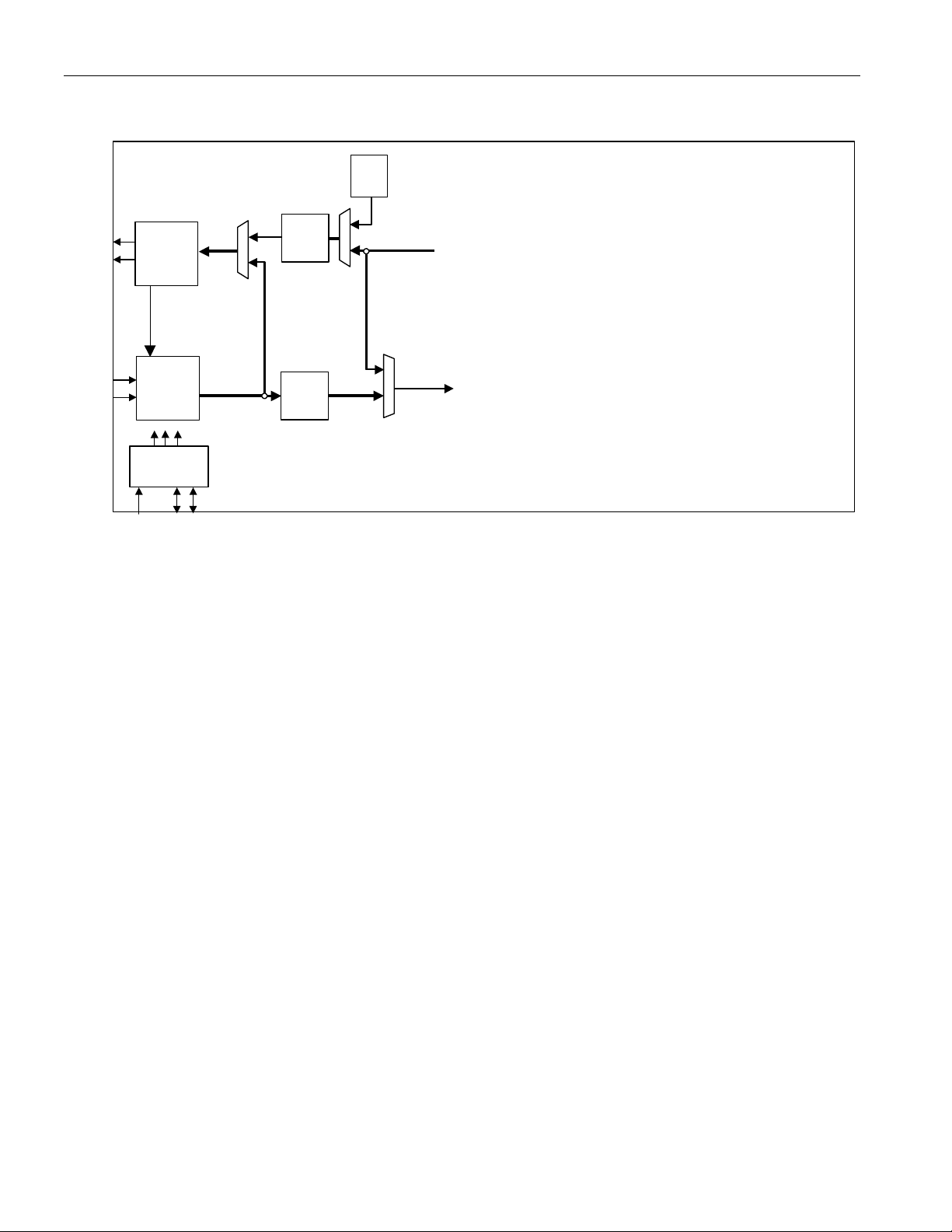
Figure 7-1. HDB3/B3ZS/AMI LIU Mode
TAIS
TUA1
B3ZS/
TXPn
TXNn
DS3/E3
Transmit
LIU
HDB3
Encoder
FROM FRAMING LOGIC
OR EXTERNAL PINS
DS3171/DS3172/DS3173/DS3174
RXPn
RXNn
ALB
DS3/E3
Receive
LIU
Clock Rate
Adapter
CLKB
CLKA
LLB
B3ZS/
HDB3
Decoder
DLB
TO FRAMING LOGIC
OR EXTERNAL PINS
n = port # (1-4)
CLKC
22
Page 23
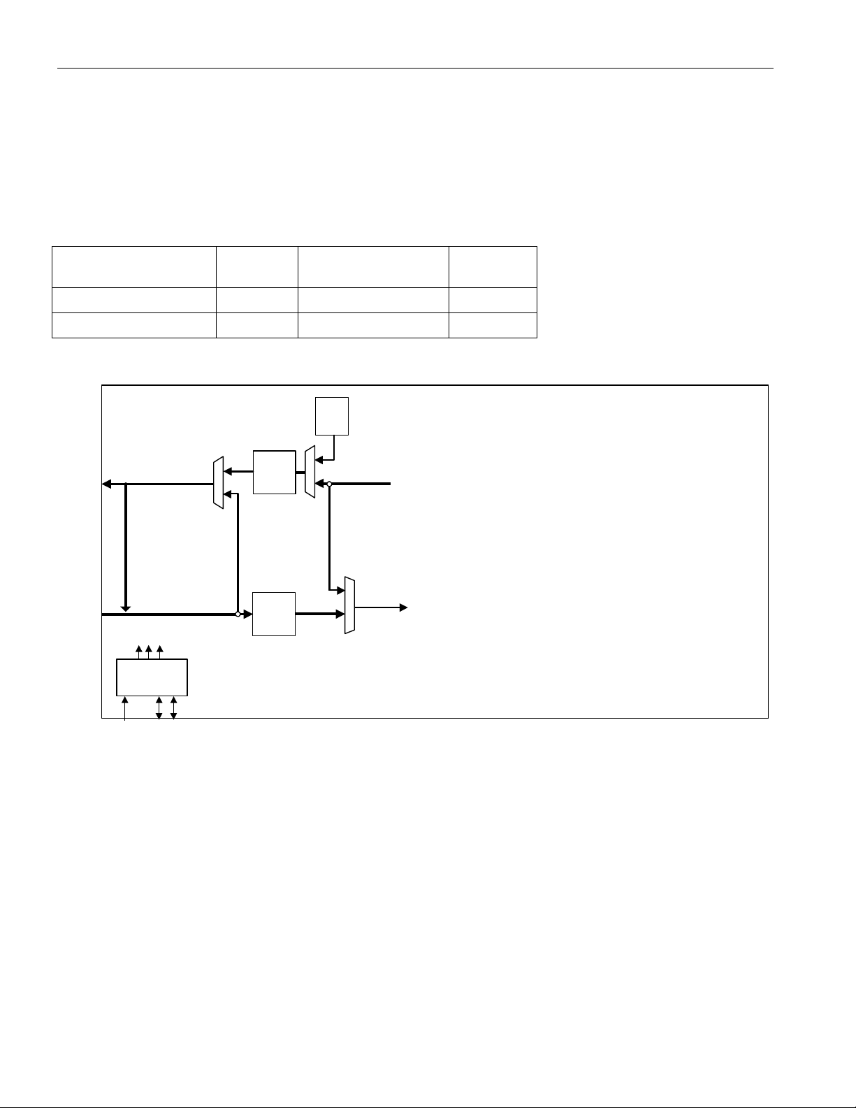
DS3171/DS3172/DS3173/DS3174
7.2 HDB3/B3ZS/AMI Non-LIU Line Interface Mode
The Non-LIU Line Interface Mode disables the LIU and a digital representation of AMI is output/input on the
TPOSn/TNEGn signals and the RPOSn/RNEGn signals. Selection between AMI and HDB3/B3ZS is made via the
LINE.TCR Register. HDB3 and B3ZS selection is controlled by the configuration selected by the FM bits. The DS3
modes select the B3ZS line code while the E3 modes select the HDB3 line code.
Table 7-2. HDB3/B3ZS/AMI Non-LIU Mode Configuration Registers
MODE LM[2:0] LINE.TCR.TZSD &
LINE.RCR.RZSD
TLEN
PORT.CR2
LIU Off, B3ZS or HDB3 000 0 1
LIU Off, AMI 000 1 1
Figure 7-2. HDB3/B3ZS/AMI Non-LIU Line Interface Mode
TAIS
TUA1
B3ZS/
TPOSn
TNEGn
TLCLKn
RLCLKn
RPOSn
RNEGn
ALB
HDB3
Encoder
LLB
B3ZS/
HDB3
Decoder
FROM FRAMING LOGIC
OR EXTERNAL PINS
DLB
TO FRAMING LOGIC
OR EXTERNAL PINS
Clock Rate
Adapter
n = port # (1-4)
CLKB
CLKA
CLKC
23
Page 24
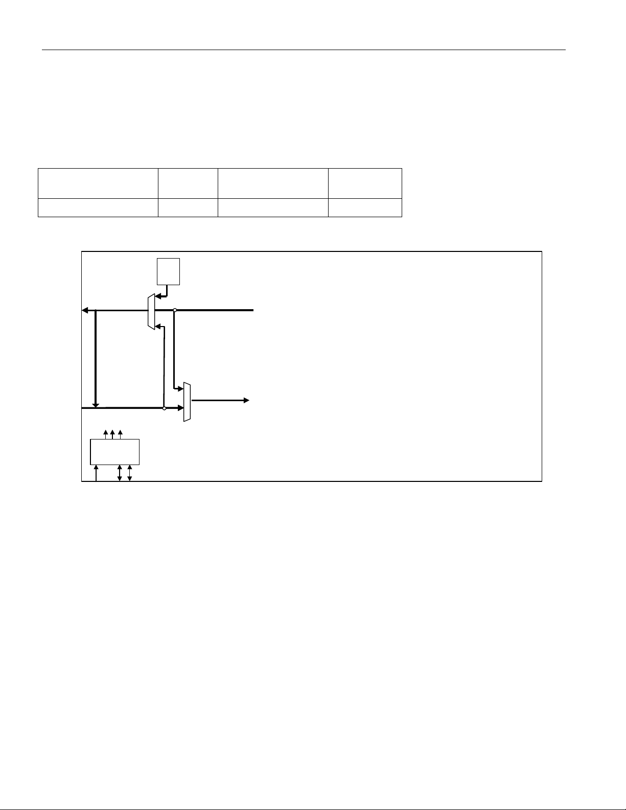
DS3171/DS3172/DS3173/DS3174
7.3 UNI Line Interface Mode
This mode is valid for all framing modes, providing a digital NRZ input/output on RDATn and TDATn and clocked
by RLCLKn and TLCLKn. The B3ZS/HDB3 decoder/encoder block is disabled except for the BPV counter, which is
used to count RLCV errors.
Table 7-3. UNI Line Interface Mode Configuration Registers
MODE LM[2:0] LINE.TCR.TZSD &
LINE.RCR.RZSD
TLEN
PORT.CR2
Unipolar Mode 1XX X 1
Figure 7-3. UNI Line Interface Mode
TUA1
TDATn
TLCLKn
RLCLKn
RDATn
ALB
Clock Rate
Adapter
LLB
DLB
FROM FRAMING LOGIC
OR EXTERNAL PINS
TO FRAMING LOGIC
OR EXTERNAL PINS
CLKA
CLKB
CLKC
n = port #
(1-4)
24
Page 25
DS3171/DS3172/DS3173/DS3174
8 PIN DESCRIPTIONS
Note: In JTAG mode, all digital pins are bidirectional to increase the effectiveness of board level ATPG patterns for
isolation of interconnect failures.
8.1 Short Pin Descriptions
Table 8-1. DS3174 Short Pin Descriptions
n=1,2,3,4 (port number); Ipu (input with pullup), Oz (output tri-stateable), (needs an external pullup or pulldown resistor to keep from floating),
Oa (Analog output), Ia (Analog input), IO (Bidirectional inout); all unused input pins without pullup should be tied low.
NAME TYPE FUNCTION
PORT 4 PORT 3 PORT 2 PORT
1
Line IO
TLCLKn O Transmit Line Clock Output V11 C11 Y8 A8
TPOSn / TDATn O Transmit Positive AMI / Data V14 C14 V4 C4
TNEGn O Transmit Negative AMI W14 B14 U4 D4
TXPn Oa Transmit Positive analog W6 B6 M2 J2
TXNn Oa Transmit Negative analog Y6 A6 M1 J1
RLCLKn I Receive Clock Input Y12 A12 W8 B8
RXPn Ia Receive Positive analog W5 B5 R2 F2
RXNn Ia Receive Negative analog Y5 A5 R1 F1
RPOSn / RDATn Ia Positive AMI / Data W15 B15 Y3 A3
RNEGn / RLCVn Ia Negative AMI / Line Code Violation Y15 A15 W3 B3
DS3/E3 Overhead Interface
TOHn I Transmit Overhead U11 D11 U8 D8
TOHENn I Transmit Overhead Enable T14 E14 T5 E5
TOHCLKn O Transmit Overhead Clock T11 E11 V8 C8
TOHSOFn O Transmit Overhead Start Of Frame T12 E12 V7 C7
ROHn O Receive Overhead T10 E10 U10 D10
ROHCLKn O Receive Overhead Clock T13 E13 U5 D5
ROHSOFn O Receive Overhead Start Of Frame U14 D14 Y2 B2
DS3/E3 Serial Data
TCLKIn I Transmit Line Clock Input Y14 A14 W4 B4
TSOFIn I Transmit Start Of Frame Input U12 D12 W7 B7
TSERn I Transmit Serial Data V13 C13 T6 E6
TCLKOn / TGCLKn O Transmit Clock Output / Gapped Clock Y13 A13 U7 D7
TSOFOn / TDENn O Transmit Framer Start Of Frame / Data Enable V12 C12 Y7 A7
RSERn O Receive Serial Data W11 B11 T9 E9
RCLKOn / RGCLKn O Receive / Clock Output / Gapped Clock Y11 A11 U9 D9
RSOFOn / RDENn O Receive Framer Start Of Frame / Data Enable W12 B12 T8 E8
PIN #
25
Page 26

DS3171/DS3172/DS3173/DS3174
NAME TYPE FUNCTION PIN #
Microprocessor Interface
D[15]
D[14]
D[13]
D[12]
D[11]
D[10]
D[9]
D[8]
D[7]
D[6]
D[5]
D[4]
D[3]
D[2]
D[1]
D[0]
A[10]
A[9]
A[8]
A[7]
A[6]
A[5]
A[4]
A[3]
A[2]
A[1]
IO Data [15:0] J5
T4
R4
P4
N4
V3
U3
T3
P3
N3
W2
U2
T2
P2
U1
P1
I Address [10:1] C3
D3
E3
G3
H3
D2
E2
G2
H2
E1
A[0] / BSWAP Address [0] / Byte Swap H1
ALE I Address Latch Enable N2
CS
RD / DS
I Chip Select (active low) L3
I Read Strobe (active low) / Data Strobe (active
K3
low)
WR / R/W
RDY
INT
I
Write Strobe (active low) / R/W Select
Oz Ready handshake (active low) K2
Oz Interrupt (active low) L4
K4
MODE I Mode select RD/WR or DS strobe mode B1
WIDTH I WIDTH select 8 or 16-bit interface L5
Misc I/O
GPIO[8]
GPIO[7]
GPIO[6]
GPIO[5]
GPIO[4]
GPIO[3]
GPIO[2]
GPIO[1]
TEST
HIZ
RST
IO General-Purpose IO [8:1] V2
V1
C2
C1
P5
R5
G5
F5
I Test enable (active low) M3
I High impedance test enable (active low) R3
I Reset (active low) B16
JTAG
JTCLK I JTAG Clock F3
JTMS Ipu JTAG Mode Select (with pull-up) F4
JTDI Ipu JTAG Data Input (with pull-up) J3
JTDO Oz JTAG Data Output G4
26
Page 27

DS3171/DS3172/DS3173/DS3174
NAME TYPE FUNCTION PIN #
JTRST
Ipu JTAG Reset (active low with pull-up) E4
CLAD
CLKA I Clock A K1
CLKB IO Clock B L1
CLKC IO Clock C L2
POWER
VSS PWR Ground, 0 Volt potential K10, K9, K8, J10, J9, J8,
H10, H9, M7, M6, L7. L6,
K7. K6, J7, J6, A1, N10,
N9, M10, M9, M8, L10, L9,
L8, R12, R11, R10, R9,
P12, P11, P10, P9, Y1,
N12, N11, M13, M12, M11,
L13, L12, L11, M15, M14,
L15, L14, K15, K14, J15,
J14, Y20, K13, K12, K11,
J13, J12, J11, H12, H11,
G12, G11, G10, G9, F12,
F11, F10, F9, A20
VDD PWR Digital 3.3V H8, H7, H6, G8, G7, G6,
F8, F7, F6, A2, R8, R7, R6,
P8, P7, P6, N8, N7, N6,
W1, R15, R14, R13, P15,
P14, P13, N15, N14, N13,
Y19, H15, H14, H13, G15,
G14, G13, F15, F14, F13,
B20
AVDDRn PWR Analog 3.3V for receive LIU on port n Y4, A4, T1, D1
AVDDTn PWR Analog 3.3V for transmit LIU on port n T7, E7, N1, J4
AVDDJn PWR Analog 3.3V for jitter attenuator on port n V6, C6, N5, G1
AVDDC PWR Analog 3.3V for CLAD K5
No Connects
NC NC No Connect, Unused A9, A10, A16–A19, B9,
B10, B13, B17–B19, C5,
C9, C10, C15–C20, D6,
D13, D15–D20, E15–E20,
F16–F20, G16–G20, H4,
H5, J16–J20, K16–K20,
L16–L20, M4, M5, M16-
M20, N16–N20, P16–P20,
R16–R20, T15–T20, U6,
U13, U15–U20, V5, V9,
V10, V16–V20, W9, W10,
W13, W16–W20, Y9, Y10,
Y15–Y18
27
Page 28
DS3171/DS3172/DS3173/DS3174
8.2 Detailed Pin Descriptions
Table 8-2. Detailed Pin Descriptions
n=1,2,3,4 (port number); Ipu (input with pullup), Oz (output tri-stateable) (needs an external pullup or pulldown resistor to keep from floating), Oa
(Analog output), Ia (analog input), IO (Bidirectional inout); all unused input pins without pullup should be tied low.
PIN NAME TYPE PIN DESCRIPTION
LINE IO
Transmit Line Clock Output
TLCLKn: This signal is available when the transmit line interface pins are enabled
(PORT.CR2.
TLCLKn O
TPOSn /
TDATn
TNEGn O
TXPn Oa
TXNn Oa
TNEG signals, but can also be used as the reference for the TSOFIn, TSERn, and TSOFOn /
TDENn signals.
This output signal can be inverted.
o DS3: 44.736 MHz +
o E3: 34.368 MHz +
Transmit Positive AMI / Data Output
TPOSn: When the port line interface is configured for B3ZS, HDB3 or AMI mode and the
transmit line interface pins are enabled (PORT.CR2.
positive pulse should be transmitted on the line. The signal is updated on the positive clock
edge of the referenced clock pin if the clock pin signal is not inverted, otherwise it is updated on
the falling edge of the clock. The signal is typically referenced to the TLCLKn line clock output
pins, but it can be referenced to the TCLKOn, TCLKIn, RLCLKn or RCLKOn pins. This output
signal can be disabled when the TX LIU is enabled.
This output signal can be inverted.
O
TDATn: When the port line interface is configured for UNI mode and the transmit line interface
pins are enabled (PORT.CR2.TLEN), the un-encoded transmit signal is output on this pin. The
signal is updated on the positive clock edge of the referenced clock pin if the clock pin signal is
not inverted, otherwise it is updated on the falling edge of the clock. The signal is typically
referenced to the TLCLK line clock output pins, but it can be referenced to the TCLKOn,
TCLKIn, RLCLKn or RCLKOn pins
This output signal can be inverted.
o DS3: 44.736 Mbps +20ppm
o E3: 34.368 Mbps +
Transmit Negative AMI / Line OH Mask
TNEGn: When the port line is configured for B3ZS, HDB3 or AMI mode and the transmit line
interface pins are enabled (PORT.CR2.
should be transmitted on the line. The signal is updated on the positive clock edge of the
referenced clock pin if the clock pin signal is not inverted, otherwise it is updated on the falling
edge of the clock. The signal is typically referenced to the TLCLKn line clock output pins, but it
can be referenced to the TCLKOn, TCLKIn, RLCLKn or RCLKOn pins.
This output signal can be inverted.
o DS3: 44.736 Mbps +20ppm
o E3: 34.368 Mbps +
Transmit Positive Analog
TXPn: This pin and the TXNn pin form a differential AMI output which is coupled to the
outbound 75Ω coaxial cable through a 2:1 step-down transformer (Figure 1-1
enabled when the TX LIU is enabled and the output is enabled to be driven. When it is not
enabled, it is in a high impedance state.
o DS3: 44.736 Mbps +
o E3: 34.368 Mbps +
Transmit Negative Analog
TXNn: This pin and the TXPn pin form a differential AMI output which is coupled to the
outbound 75Ω coaxial cable through a 2:1 step-down transformer (Figure 1-1
enabled when the TX LIU is enabled and the output is enabled to be driven. When it is not
enabled, it is in a high impedance state.
o DS3: 44.736 Mbps +
o E3: 34.368 Mbps +
TLEN). This clock is typically used as the clock reference for the TDATn and
20 ppm
20 ppm
TLEN), a high on this pin indicates that a
20ppm
TLEN), a high on this pin indicates that a negative pulse
20ppm
). This output is
20ppm
20ppm
). This output is
20ppm
20ppm
28
Page 29

PIN NAME TYPE PIN DESCRIPTION
Receive Positive analog
RXPn: This pin and the RXNn pin form a differential AMI input which is coupled to the outbound
RXPn Ia
RXNn Ia
RLCLKn I
RPOSn /
RDATn
RNEGn /
RLCVn
Iad
Iad
75Ω coaxial cable through a 2:1 step-up transformer (Figure 1-1
RX LIU is enabled and is ignored when the LIU is disabled.
o DS3: 44.736 Mbps +20ppm
o E3: 34.368 Mbps +
Receive Negative analog
RXNn: This pin and the RXPn pin form a differential AMI input which is coupled to the outbound
75Ω coaxial cable through a 2:1 step-up transformer (Figure 1-1
LIU is enabled and is ignored when the LIU is disabled.
o DS3: 44.736 Mbps +
o E3: 34.368 Mbps +
Receive Line Clock Input
RLCLKn: This clock is typically used for the reference clock for the RPOSn / RDATn, RNEGn /
RLCVn signals but can also be used as the reference clock for the RSERn, RSOFOn / RDENn,
TSOFIn, TSERn, TSOFOn / TDENn, TPOSn / TDATn and TNEGn signals. This input is ignored
when the LIU is enabled.
This input signal can be inverted.
o DS3: 44.736 MHz +
o E3: 34.368 MHz +
Receive Positive AMI / Data
RPOSn: When the port line is configured for B3ZS, HDB3 or AMI mode and the LIU is disabled,
a high on this pin indicates that a positive pulse has been detected using an external LIU. The
signal is sampled on the positive clock edge of the referenced clock pin if the clock pin signal is
not inverted, otherwise it is sampled on the falling edge of the clock. The signal is typically
referenced to the RLCLKn line clock input pins, but it can be referenced to the RCLKOn output
pins.
This input signal can be inverted.
RDATn: When the port line interface is configured for UNI mode, the un-encoded receive signal
is input on this pin. The signal is sampled on the positive clock edge of the referenced clock pin
if the clock pin signal is not inverted, otherwise it is sampled on the falling edge of the clock.
The signal is typically referenced to the RLCLKn line clock input pins, but it can be referenced
to the RCLKOn output pins.
This input signal can be inverted.
o DS3: 44.736 Mbps +
o E3: 34.368 Mbps +
Receive Negative AMI / Line Code Violation / Line OH Mask input
RNEGn: When the port line is configured for B3ZS, HDB3 or AMI mode and the LIU is disabled,
a high on this pin indicates that a negative pulse has been detected using an external LIU. The
signal is sampled on the positive clock edge of the referenced clock pin if the clock pin signal is
not inverted, otherwise it is sampled on the falling edge of the clock. The signal is typically
referenced to the RLCLKn line clock input pins, but it can be referenced to the RCLKOn output
pins.
This input signal can be inverted.
o DS3: 44.736 Mbps +
o E3: 34.368 Mbps +
RLCVn: When the port line interface is configured for UNI mode, the BPV counter in the
encoder/decoder block is incremented each clock when this signal is high. The signal is
sampled on the positive clock edge of the referenced clock pin if the clock pin signal is not
inverted, otherwise it is sampled on the falling edge of the clock. The signal is typically
referenced to the RLCLKn line clock input pins, but it can be referenced to the RCLKOn output
pins.
This input signal can be inverted.
20ppm
20ppm
20ppm
20 ppm
20 ppm
20ppm
20ppm
20ppm
20ppm
DS3171/DS3172/DS3173/DS3174
). This input is used when the
). This input is used when the
29
Page 30

PIN NAME TYPE PIN DESCRIPTION
DS3/E3 OVERHEAD INTERFACE
Transmit Overhead
TOHn: When the port framer is configured for one of the DS3 or E3 framing modes, this signal
will be used to over-write the DS3 or E3 framing overhead bits when TOHENn is active. In T3
TOHn I
TOHENn I
TOHCLKn O
TOHSOFn O
ROHn O
ROHCLKn O
ROHSOFn O
mode, the X-bits, P-bits, M-bits, F-bits, and C-bits are input. In G.751 E3 mode, all of the FAS,
RAI, and National Use bits are input. In G.832 E3 mode, all of the FA1, FA2, EM, TR, MA, NR,
and GC bytes are input. The TOHSOFn signal marks the start of the framing bit sequence. This
signal is sampled at the same time as the TOHCLKn signal transitions high to low.
This signal can be inverted.
Transmit Overhead Enable / Start Of Frame Input
TOHENn: When the port framer is configured for one of the DS3 or E3 framing modes, this
signal will be used the determine which DS3 or E3 framing overhead bits to over-write with the
signal on the TOHn pins. The TOHSOFn signal marks the start of the framing bit sequence.
This signal is sampled at the same time as the TOHCLKn signal transitions high to low.
This signal can be inverted.
Transmit Overhead Clock
TOHCLKn: When the port framer is configured for one of the DS3 or E3 framing modes, this
clock is used for the transmit overhead port signals TOHn, TOHENn and TOHSOFn. The
TOHSOFn output signal is updated and the TOHn and TOHENn input signals are sampled at
the same time this clock signal transitions from high to low. The external logic is expected to
sample TOHSOFn signal and update the TOHn and TOHENn signals on the rising edge of this
clock signal. This clock is a low frequency clock.
This signal can be inverted.
Transmit Overhead Start Of Frame
TOHSOFn: When the port framer is configured for one of the DS3 or E3 framing modes, this
signal is used to mark the start of a DS3 or E3 overhead sequence on the TOHn pins. In T3
mode, the first X-bit is marked. In G.751 E3 mode, the first bit of the FAS word is marked. In
G.832 E3 mode, the first bit of the FA1 byte is marked. The sequence starts on the same high
to low transition of the TOHCLKn clock that this signal is high. This signal is updated at the
same time as the TOHCLKn signal transitions high to low.
This signal can be inverted.
Receive Overhead
ROHn: When the port framer is configured for one of the DS3 or E3 framing modes, this signal
outputs the value of the receive overhead bits. The ROHSOFn signal marks the start of the
framing bit sequence. In T3 mode, the X-bits, P-bits, M-bits, F-bits, and C-bits are output (Note:
In M23 mode, the C-bits are extracted even though they are marked as data at the payload
interface). In G.751 E3 mode, all of the FAS, RAI, and National Use bits are output. In G.832
E3 mode, all of the FA1, FA2, EM, TR, MA, NR, and GC bytes are output.
This signal is updated at the same time as the ROHCLKn signal transitions high to low.
This signal can be inverted.
Receive Overhead Clock
ROHCLKn: When the port framer is configured for one of the DS3 or E3 framing modes, this
clock is used for the receive overhead port signals ROHn and ROHSOFn. The ROHSOFn and
ROHn output signals are updated at the same time this clock signal transitions from high to low.
The external logic is expected to sample ROHSOFn and ROHn signal on the rising edge of this
clock signal. This clock is a low frequency clock.
This signal can be inverted.
Receive Overhead Start Of Frame
ROHSOFn: When the port framer is configured for one of the DS3 or E3 framing modes this
signal is used to mark the start of a DS3 or E3 overhead sequence on the ROHn pins. In T3
mode, the first X-bit is marked. In G.751 E3 mode, the first bit of the FAS word is marked. In
G.832 E3 mode, the first bit of the FA1 byte is marked. The sequence starts on the same high
to low transition of the ROHCLKn clock that this signal is high. This signal is updated at the
same time as the ROHCLKn signal transitions high to low.
This signal can be inverted.
DS3171/DS3172/DS3173/DS3174
30
Page 31

PIN NAME TYPE PIN DESCRIPTION
DS3/E3 SERIAL DATA OVERHEAD INTERFACE
Transmit Line Clock Input
TCLKIn: This clock is typically used for the reference clock for the TSOFIn, TSERn, and
TSOFOn / TDENn signals but can also be used as the reference for the TPOSn / TDATn and
TCLKIn I
TSOFIn I
TSERn I
TCLKOn /
TGCLKn
TNEGn signals. This clock is not used when the part is in loop time mode or the CLAD clocks
are used as the transmit clock source. (PORT.CR3.CLADC)
This input signal can be inverted.
o DS3: 44.736 MHz +
o E3: 34.368 MHz +
Transmit Start Of Frame Input
See Table 10-20.
TSOFIn: This signal can be used to align the start of the DS3 or E3 frames on the TSERn pin to
an external signal. In SCT modes, the TSOFIn signal can be used to align the start of frame
signal position on the TSERn/TOHn
Pin to the rising edge of a signal on this pin. The signal edge does not need to occur on every
frame and can be tied high or low. The signal is sampled on the positive clock edge of the
referenced clock pin if the clock pin signal is not inverted, otherwise it is sampled on the falling
edge of the clock. The signal is typically referenced to the TCLKIn transmit clock input pins, but
it can be referenced to the TLCLKn, TCLKOn, RCLKOn and RLCLKn clock pins.
This signal can be inverted.
Transmit Serial Data
TSERn: When the port framer is configured for either the DS3 or E3 SCT modes, this pin is
used as the source of the DS3/E3 payload data. When the port is configured for a clear channel
mode, this pin is used as the source of the DS3/E3 data signal. The signal is sampled on the
positive clock edge of the referenced clock pin if the clock pin signal is not inverted, otherwise it
is sampled on the falling edge of the clock. The signal is typically referenced to the TCLKIn
transmit clock input pins, but it can be referenced to the TLCLKn, TCLKOn / TGCLKn, RCLKOn
and RLCLKn clock pins
This signal can be inverted.
o DS3: 44.736 Mbps +
o E3: 34.368 Mbps +
Transmit Clock Output / Gapped Clock
See Table 10-22
TCLKOn: When the port is configured for unframed SCT or framed SCT modes and TCLKOn is
selected, this clock output is enabled. This clock is the same clock as the internal framer
transmit clock. This clock is typically used for the reference clock for the TSOFIn, TSERn, and
TSOFOn / TDENn signals but can also be used as the reference for the TPOSn / TDATn and
TNEGn signals.
This signal can be inverted.
O
o DS3: 44.736 MHz +
o E3: 34.368 MHz +
TGCLKn: When the port is configured for framed DS3/E3 mode and TGCLKn is selected, this
gated output clock is enabled. This gapped clock is the same clock as the internal framer
transmit clock and is gated by TDENn. This clock is typically used for the reference clock for the
TSERn signal.
This signal can be inverted.
.
20 ppm
20 ppm
20ppm
20ppm
20 ppm
20 ppm
DS3171/DS3172/DS3173/DS3174
31
Page 32

PIN NAME TYPE PIN DESCRIPTION
Framer Start Of Frame / Data Enable
TSOFOn /
TDENn
RSERn O
RCLKOn /
RGCLKn
RSOFOn /
RDENn
O
O
O
See Table 10-21
TSOFOn: When the port framer is configured for the DS3 or E3 framed modes and the
TSOFOn pin function is selected, this signal is used to indicate the start of the DS3/E3 frame on
the TSERn pin. This signal pulses high three clocks before the first overhead bit in a DS3 or E3
frame that will be input on TSERn. The signal is updated on the positive clock edge of the
referenced clock pin if the clock pin signal is not inverted, otherwise it is updated on the falling
edge of the clock. The signal is typically referenced to the TCLKIn transmit clock input pins, but
it can be referenced to the TLCLKn, TCLKOn, RCLKOn and RLCLKn clock pins.
This signal can be inverted.
TDENn: When the port framer is configured for the DS3 or E3 framed modes and the TDENn
pin function is selected, this signal is used to mark the DS3/E3 frame bits on the TSERn pin.
The signal goes high three clocks before the start of DS3/E3 payload bits and goes low three
clocks before the end of the DS3/E3 payload bits. The signal is updated on the positive clock
edge of the referenced clock pin if the clock pin signal is not inverted, otherwise it is updated on
the falling edge of the clock. The signal is typically referenced to the TCLKIn transmit clock
input pins, but it can be referenced to the TLCLKn, TCLKOn, RCLKOn and RLCLKn clock pins.
This signal can be inverted.
Receive Serial Data
RSERn: When the port framer is configured for the DS3 or E3 framed modes, this pin outputs
the receive data signal from the LIU or receive line pins. The signal is updated on the positive
clock edge of the referenced clock pin if the clock pin signal is not inverted, otherwise it is
updated on the falling edge of the clock. The signal is typically referenced to the RCLKOn
receive clock output pin, but it can be referenced to the RGCLKn and RLCLKn clock pins.
This signal can be inverted
o DS3: 44.736 Mbps +
o E3: 34.368 Mbps +
Receive Clock Output / Gapped Clock
See Table 10-24
RCLKOn: When the port framer is configured for the DS3 or E3 framed modes and RCLKOn is
selected, this clock output signal is active. It is the same as the internal receive framer clock.
This clock is typically used for the reference clock for the RSERn, RSOFOn / RDENn signals
but can also be used as the reference for the RPOSn / RDATn, RNEGn / RLCVn, TSOFIn,
TSERn, TSOFOn / TDENn, TPOSn / TDATn and TNEGn signals.
This signal can be inverted.
o DS3: 44.736 MHz +
o E3: 34.368 MHz +
RGCLKn: When the port is configured for DS3/E3 framed mode and RGCLKn is selected, this
gated clock output signal is active. It is the same as the internal receive framer clock gated by
RDENn. This clock is typically used for the reference clock for the RSERn.
This signal can be inverted
Receive Framer Start Of Frame /Data Enable
See Table 10-23
RSOFOn: When the port framer is configured for the DS3 or E3 framed modes and the
RSOFOn pin function is enabled, this signal is used to indicate the start of the DS3/E3 frame.
This signal indicates the first DS3/E3 overhead bit on the RSERn pin when high. The signal is
updated on the positive clock edge of the referenced clock pin if the clock pin signal is not
inverted, otherwise it is updated on the falling edge of the clock. The signal is typically
referenced to the RCLKOn receive clock output pin, but it can be referenced to the RLCLKn
clock input pin.
This signal can be inverted.
RDENn: When the port framer is configured for the DS3 or E3 framed modes and the RDENn
pin function is enabled, this signal is used to indicate the DS3/E3 payload bit positions of the
data on the RSERn pin. The signal goes high during each DS3/E3 payload bit and goes low
during each DS3/E3 overhead bit. The signal is updated on the positive clock edge of the
referenced clock pin if the clock pin signal is not inverted, otherwise it is updated on the falling
edge of the clock. The signal is typically referenced to the RCLKOn receive clock output pin,
but it can be referenced to the RLCLKn clock input pin.
This signal can be inverted.
.
20ppm
20ppm
.
20 ppm
20 ppm
.
DS3171/DS3172/DS3173/DS3174
32
Page 33

PIN NAME TYPE PIN DESCRIPTION
MICROPROCESSOR INTERFACE
Bi-directional 16 or 8-bit data bus
This bus is tri-state when RST pin is low or CS pin is high.
D[15:0] IO
A[10:1] I
A[0] /
BSWAP
ALE I
CS
RD /
DS
WR /
R/W
RDY
INT
MODE I
WIDTH I
Oz
Oz
D[15:0]: A 16-bit or 8-bit data bus used to input data during register writes, and data outputs
during register reads. The upper 8 bits are not used and never driven in 8-bit bus mode.
Weak pull up resistors or bus holders should be used for each pin.
Address bus (minus LSB)
A[10:1]: identifies the specific 16 bit registers, or group of 8 bit registers, being accessed. A[10]
must be tied to ground for the DS3181 and DS3182 versions.
Address bus LSB / Byte Swap
A[0]: This signal is connected to the lower address bit in 8-bit systems. (WIDTH=0)
1 = Output register bits 15:8 on D[7:0], D[15:8] not driven
BSWAP: This signal is tied high or low in 16-bit systems.
(WIDTH=1)
Address Latch Enable
ALE: This signal is used to latch the address on the A[10:0] pins in multiplexed address
systems. When it is high the address is fed through the address latch to the internal logic.
When it transitions to low, the address is latched and held internally until the signal goes back
high. ALE should be tied high for non-multiplexed address systems.
Chip Select (active low)
I
CS: This signal must be low during all accesses to the registers
Read Strobe (active low) / Data Strobe (active low)
RD: Read Strobe mode (MODE=0):
I
DS: Data Strobe mode (MODE=1):
Write Strobe (active low) / R/W Select
WR: Write Strobe mode (MODE=0):
I
R/W: Data Strobe mode (MODE=1):
Ready handshake (active low)
RDY: This ready signal is driven low when the current read or write cycle is in progress. When
the current read or write cycle is not ready it is driven high. When device is not selected, it is not
driven.
Interrupt (active low)
This signal is tri-state when RST pin is low.
INT: This interrupt signal is driven low when an event is detected on any of the enabled
interrupt sources in any of the register banks. When there are no active and enabled interrupt
sources, the pin can be programmed to either drive high or not drive high. The reset default is
to not drive high when there is no active and enabled interrupt source. All interrupt sources are
disabled when RST=0 and they must be programmed to be enabled.
Mode select RD/WR or DS strobe mode
MODE: 1 = Data Strobe Mode, 0 = Read/Write Strobe Mode
Data bus width select 8 or 16-bit interface
WIDTH: 1 = 16-bits, 0 = 8 bits
0 = Output register bits 7:0 on D[7:0], D[15:8] not driven
1 = Output register bits 15:8 on D[7:0], 7:0 on D[15:8]
0 = Output register bits 7:0 on D[7:0], 15:8 on D[15:8]
RD is low during a register read.
DS is low during either a register read or a write.
WR is low during a register write.
R/W is high during a register read cycle, and low during a register write cycle.
DS3171/DS3172/DS3173/DS3174
33
Page 34

PIN NAME TYPE PIN DESCRIPTION
MISC I/O
General-Purpose IO 1
GPIO1 IO
GPIO2 IO
GPIO3 IO
GPIO4 IO
GPIO5 IO
GPIO6 IO
GPIO7 IO
GPIO8 IO
TEST
HIZ
RST
JTCLK I
JTMS Ipu
JTDI Ipu
JTDO Oz
JTRST
Ipu
GPIO1: This signal is configured to be a general-purpose IO pin, or an alarm output signal for
port 1.
General-Purpose IO 2
GPIO2: This signal is configured to be a general-purpose IO pin, or the 8KREFO output signal,
or an alarm output signal for port 1.
General-Purpose IO 3
GPIO3: This signal is configured to be a general-purpose IO pin, or an alarm output signal for
port 2.
General-Purpose IO 4
GPIO4: This signal is configured to be a general-purpose IO pin, or the 8KREFI input signal, or
an alarm output signal for port 2. When configured for 8KREFI mode the signal frequency
should be 8,000 Hz +/- 500 ppm and about 50% duty cycle.
General-Purpose IO 5
GPIO5: This signal is configured to be a general-purpose IO pin, or an alarm output signal for
port 3.
General-Purpose IO 6
GPIO6: This signal is configured to be a general-purpose IO pin, or the TMEI input signal, or an
alarm output signal for port 3. When configured for TMEI input, the signal low time and high
time must be greater than 500 ns.
General-Purpose IO 7
GPIO7: This signal is configured to be a general-purpose IO pin, or an alarm output signal for
port 4.
General-Purpose IO 8
GPIO8: This signal is configured to be a general-purpose IO pin, or the PMU input signal, or an
alarm output signal for port 4. When configured for PMU input, the signal low time and high time
must be greater than 500 ns.
Test enable (active low)
I
TEST: This signal enables the internal scan test mode when low. For normal operation tie high.
This is an asynchronous input.
High impedance test enable (active low)
I
HIZ: This signal puts all digital output and bi-directional pins in the high impedance state when
it low and JTRST is low. For normal operation tie high. This is an asynchronous input.
Reset (active low)
RST: This signal resets all the internal processor registers and logic when low. This pin should
I
be low while power is applied and set high after the power is stable. This is an asynchronous
input.
JTAG
JTAG Clock
JTCLK: This clock input is typically a low frequency (less than 10 MHz) 50% duty cycle clock
signal.
JTAG Mode Select (with pull-up)
JTMS: This input signal is used to control the JTAG controller state machine and is sampled on
the rising edge of JTCLK.
JTAG Data Input (with pull-up)
JTDI: This input signal is used to input data into the register that is enabled by the JTAG
controller state machine and is sampled on the rising edge of JTCLK.
JTAG Data Output
JTDO: This output signal is the output of an internal scan shift register enabled by the JTAG
controller state machine and is updated on the falling edge of JTCLK. The pin is in the high
impedance mode when a register is not selected or when the JTRST signal is high. The pin
goes into and exits the high impedance mode after the falling edge of JTCLK
JTAG Reset (active low with pullup)
JTRST: This input forces the JTAG controller logic into the reset state and forces the JTDO pin
into high impedance when low. This pin should be low while power is applied and set high after
the power is stable. The pin can be driven high or low for normal operation, but must be high for
JTAG operation.
DS3171/DS3172/DS3173/DS3174
34
Page 35

PIN NAME TYPE PIN DESCRIPTION
CLAD
Clock A
CLKA I
CLKB IO
CLKC IO
VSS PWR
VDD PWR
AVDDRn PWR
AVDDTn PWR
AVDDJn PWR
AVDDC PWR
CLKA: This clock input is a DS3 signal(44.736MHz +/-20ppm) when the CLAD is disabled or it
is one of the CLAD reference clock signals when the CLAD is enabled.
Clock B
CLKB: This pin is a E3(34.368 MHz +/-20 ppm) input signal when the CLAD is disabled or it
can be enabled to output a generated clock when the CLAD is enabled. The pin is driven low
when it is not selected to output a clock signal and the CLAD is enabled. Refer to Table 10-11.
Clock C
CLKC: This pin is a STS-1 (51.84 MHz +/-20ppm) input signal when the CLAD is disabled or it
can be enabled to output a generated clock when the CLAD is enabled. The pin is driven low
when it is not selected to output a clock signal and the CLAD is enabled. Refer to Table 10-11.
POWER
Ground, 0 Volt potential
Common to digital core, digital IO and all analog circuits
Digital 3.3V
Common to digital core and digital IO
Analog 3.3V for receive LIU on port n
Powers receive LIU on port n
Analog 3.3V for transmit LIU on port n
Powers transmit LIU on port n
Analog 3.3V for jitter attenuator on port n
Powers jitter attenuator on port n
Analog 3.3V for CLAD
Powers clock rate adapter common to all ports
DS3171/DS3172/DS3173/DS3174
35
Page 36
DS3171/DS3172/DS3173/DS3174
8.3 Pin Functional Timing
8.3.1 Line IO
8.3.1.1 B3ZS/HDB3/AMI Mode Transmit Pin Functional Timing
There is no suggested time alignment between the TXPn, TXNn and TX LINE signals and the TLCLKn clock signal.
The TX DATA signal is not a readily available signal, it is meant to represent the data value of the other signals.
The TXPn and TXNn signals are only available when the line is in B3ZS/HDB3 or AMI mode and the LIU is
enabled. The TPOSn, TNEGn and TLCLKn signals are only available when the line is in B3ZS/HDB3 or AMI mode
and the transmit line pins are enabled. The TPOSn, TNEGn and TLCLKn pins can be enabled at the same as the
LIU is enabled.
The TPOSn and TNEGn signals change a small delay after the positive edge of the reference clock if the clock pin
is not inverted; otherwise they change after the negative edge. The TLCLKn clock pin is the clock reference
typically used for the TPOSn and TNEGn signals, but they can be time referenced to the TCLKIn, TCLKOn,
RLCLKn or RCLKOn clock pins. The TPOSn and TNEGn pins can be inverted, but the polarity of TXPn and TXNn
cannot be inverted.
TXPn and TXNn are differential analog output pins. They are biased around ½ VDD and pulse above and below
the bias voltage by about 1 Volt. These signals are connected to the windings of a 1:2 step down transformer and
the other winding of the transformer creates the TX LINE signal. The TX LINE signal is a bipolar signal that pulses
about 1 Volt positive and 1 Volt negative above and below ground (0 volts). See Figure 1-1
external connections.
for a diagram of the
Figure 8-1
and Figure 8-2 show the relationship between the analog and the digital outputs.
Figure 8-1. TX Line IO B3ZS Functional Timing Diagram
TLCLK
(TX DATA)
TPOS
TNEG
TXP
TXN
(TX LINE)
BIAS V
0 V
B
BV
B
+
-
B
V
V
V
B3ZS CODEWORD
36
Page 37

Figure 8-2. TX Line IO HDB3 Functional Timing Diagram
TLCLK
(TX DATA)
TPOS
DS3171/DS3172/DS3173/DS3174
TNEG
TXP
TXN
(TX LINE)
BIAS V
0 V
B
BV
B
+
-
BV
V
V
HDB3 CODEWORD
8.3.1.2 B3ZS/HDB3/AMI Mode Receive Pin Functional Timing
There is no suggested time alignment between the RXPn, RXNn and RX LINE signals and the RLCLKn clock
signal. The RX DATA signal is not an always readily available signal, it is meant to represent the data value of the
other signals. The signal on RSERn will be the same as the RX DATA signal except delayed.
The RXPn and RXNn pins are only available when the line is in B3ZS/HDB3 or AMI mode and the LIU is enabled.
The RPOSn, RNEGn and RLCLKn pins are only available when the line is in B3ZS/HDB3 or AMI mode and the LIU
is disabled.
The RPOSn and RNEGn signals are sampled at the rising edge of the reference clock signal if the clock pin is not
inverted; otherwise they are sampled at the negative edge. The RLCLKn clock pin is the clock reference used for
the RPOSn and RNEGn signals. The RPOSn and RNEGn pins can be inverted.
RXPn and RXNn are differential analog input pins. They are biased around ½ VDD and pulse above and below the
bias voltage by about 1 Volt with zero cable length. These signals are connected to the windings of a 1:2 step up
transformer and the other winding of the transformer is connected to the RX LINE signal. The RX LINE signal is a
bipolar signal that pulses about 1 Volt positive and 1 Volt negative above and below ground (0 volts) with zero
cable length. See Figure 1-1
for a diagram of the external connections.
Figure 8-3
and Figure 8-4 show the relationship between the analog and the digital outputs.
Figure 8-3. RX Line IO B3ZS Functional Timing Diagram
RLCLK
(RX DATA)
RPOS
V
V
V
B3ZS CODEWORD
37
RNEG
RXP
RXN
(RX LINE)
BIAS V
0 V
B
BV
B
+
-
B
Page 38

Figure 8-4. RX Line IO HDB3 Functional Timing Diagram
RLCLK
(RX DATA)
RPOS
DS3171/DS3172/DS3173/DS3174
RNEG
RXP
RXN
(RX LINE)
BIAS V
0 V
B
BV
B
+
-
BV
V
V
HDB3 CODEWORD
8.3.1.3 UNI Mode Transmit Pin Functional Timing
The TDATn pin is available when the line interface is in the UNI mode and the transmit line pins are enabled
The TDATn signal changes a small delay after the positive edge of the reference clock signal if the clock pin is not
inverted, other wise they change after the negative edge. The TLCLKn clock pin is the clock reference typically
used for the TDATn signal, but the TDATn can be time referenced to the TCLKIn, TCLKOn, RLCLKn or RCLKOn
clock pins. The TDATn pins can be inverted. See Figure 8-5
.
Figure 8-5. TX Line IO UNI Functional Timing Diagram
TLCLK
TDAT
8.3.1.4 UNI Mode Receive Pin Functional Timing
The RDATn pin is available when the line interface is in the UNI mode. The RLCVn pin is available when the line
interface is in the UNI
All bits on the RDATn pin, will come out the RSERn pin, if the RSERn pin is enabled.
The signal on the RLCVn pin enables the BPV counter, which is in the line interface, to increment each clock it is
high.
The RDATn and RLCVn signals are sampled at the rising edge of the reference clock signal if the clock pin is not
inverted; otherwise they are sampled at the negative edge. The RLCLKn clock pin is the clock reference used for
the RDATn and RLCVn signals. The RDATn and RLCVn pins can be inverted. See Figure 8-6
.
38
Page 39
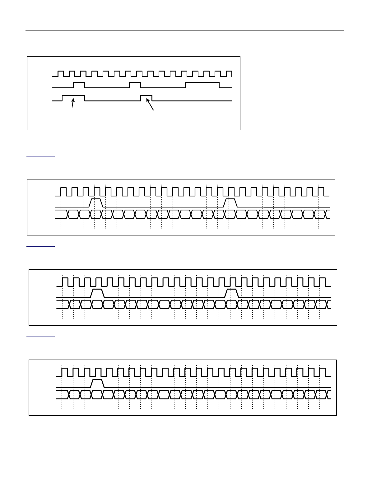
Figure 8-6. RX Line IO UNI Functional Timing Diagram
RLCLK
RDAT
RLVC
INC BPV COUNTER TWICE INC BPV COUNTER ONCE
8.3.2 DS3/E3 Framing Overhead Functional Timing
Figure 8-7 shows the relationship between the DS3 receive overhead port pins.
Figure 8-7. DS3 Framing Receive Overhead Port Timing
ROHCLK
ROHSOF
FAS
ROH
Figure 8-8
FAS
FAS
FAS
FAS
3
2
4
FAS
10
NA
1
FAS
FAS
FAS7FAS
6
5
FAS
FAS
9
8
A
10
1234567891011121314 16171819202122232415
shows the relationship between the E3 G.751 receive overhead port pins.
FAS
N
1
DS3171/DS3172/DS3173/DS3174
2
FAS3FAS
FAS
4
5
FAS
FAS
8
6
FAS
FAS
10
9
Figure 8-8. E3 G.751 Framing Receive Overhead Port Timing
ROHCLK
ROHSOF
ROH
FAS
10
FAS
FAS
FAS
3
2
4
FAS
FAS
5
8
FAS7FAS
6
FAS
FAS
A
10
9
FAS
NA
1
FAS
N
1
1 2 3 4 5 6 7 8 9 10 11 12 13 14 16 17 18 19 20 21 22 23 2415
Figure 8-9
shows the relationship between the E3 G.832 receive overhead port pins.
Figure 8-9. E3 G.832 Framing Receive Overhead Port Timing
ROHCLK
ROHSOF
ROH
FA1
FA1
FA1
3
2
4
FA1
FA1
FA17FA1
6
5
FA2
8
1
GC
7
6
1
8
FA1
GC
GC
FA2
FA2
3
2
1 2 3 4 5 6 7 8 9 10 11 12 13 14 16 17 18 19 20 21 22 23 2415
FA2
FA2
5
4
FAS
FA2
2
6
FAS3FAS
FA27FA2
4
5
8
6
FAS
FAS
FAS
FAS
FAS
10
9
8
1
3
2
EM
EM
EM
EM
EM
5
4
39
Page 40

Figure 8-10
shows the relationship between the DS3 transmit overhead port pins.
Figure 8-10. DS3 Framing Transmit Overhead Port Timing
TOHCLK
TOHSOF
TOHEN
TOH
X1 F13C12F12 C13 F14 F21
F74C73F73
F11
C11
X2
C21
F22
1 2 3 4 5 6 7 8 9 1011121314 16171819202122232415
Figure 8-11
shows the relationship between the E3 G.751 transmit overhead port pins.
Figure 8-11. E3 G.751 Framing Transmit Overhead Port Timing
TOHCLK
TOHSOF
DS3171/DS3172/DS3173/DS3174
F23C22
C23 F24
F31 C31P1 C32F32
TOHEN
TOH
FAS
10
FAS
FAS
FAS
3
2
4
FAS
FAS
5
8
FAS7FAS
6
FAS
FAS
A
10
9
FAS
NA
1
FAS
N
1
2
FAS3FAS
FAS
4
6
5
FAS
8
FAS
9
9
FAS
FAS
FAS
1234567891011121314 16171819202122232415
Figure 8-12
shows the relationship between the E3 G.832 transmit overhead port pins.
Figure 8-12. E3 G.832 Framing Transmit Overhead Port Timing
TOHCLK
TOHSOF
TOHEN
TOH
FA1
FA1
FA1
3
2
4
FA1
FA1
FA17FA1
6
5
FA2
8
1
GC
7
6
1
8
FA1
GC
GC
FA2
FA2
FA2
3
2
4
1234567891011121314 16171819202122232415
8.3.3 DS3/E3 Serial Data Interface
8.3.3.1 DS3/E3 SCT Mode Transmit Serial Interface Pin Functional Timing
The TSERn pin is used to input DS3 or E3 payload data bits in all framing modes as well as the C-bits, which can
be treated as payload, in DS3 M23 and E3 G.751 framing modes. The TDENn signal is used to determine the DS3
or E3 payload bit positions on TSERn. The TDENn signal goes high three clocks before the first bit of a payload
sequence is clocked into the TSERn pin and it goes low three clocks before the payload sequence is stopped
being clocked in to the TSERn pin. The TSOFOn signal pulses high three clocks before the start of the DS3 or E3
overhead bit position on TSERn. The TSOFIn pin is used to set the DS3 or E3 frame position. When the TSOFIn
pin transitions low to high, the first DS3/E3 overhead bit position on TSERn will be forced to align to it
FA2
FA2
FA27FA2
6
5
EM
8
1
EM
EM
3
2
EM
EM
5
4
Figure 8-13
to Figure 8-15 show the relationship between the SCT transmit port pins.
40
Page 41
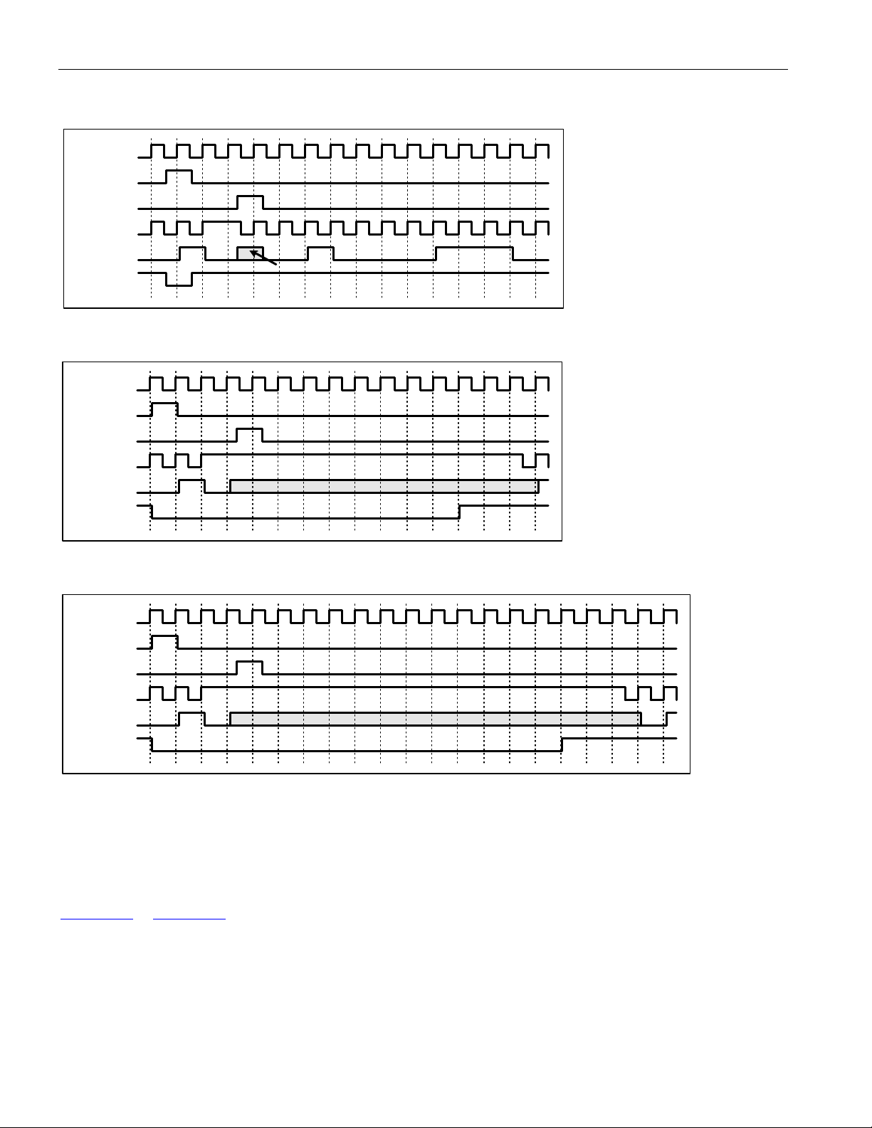
DS3171/DS3172/DS3173/DS3174
Figure 8-13. DS3 SCT Mode Transmit Serial Interface Pin Timing
TCLKO or
TCLKI
TSOFO
TSOFI
DS3 TGCLK
DS3 TSER
DS3 TDEN
TSER DATA IS OVERWRITTEN WITH OH
6 7 8 9 10 11 12 1312345 1415
Figure 8-14. E3 G.751 SCT Mode Transmit Serial Interface Pin Timing
TCLKO or
TCLKI
TSOFO
TSOFI
E3 TGCLK
E3 TSER
E3 TDEN
TSER DATA IS OVERWRITTEN WITH OH
6 7 8 9 10 11 12 1312345 1415
Figure 8-15. E3 G.832 SCT Mode Transmit Serial Interface Pin Timing
TCLKO or
TCLKI
TSOFO
TSOFI
E3 TGCLK
E3 TSER
E3 TDEN
TSER DATA IS OVERWRITTEN WITH OH
6789101112131 2 3 4 5 14 15 16 17 18 19 20
8.3.3.2 DS3/E3 SCT Mode Receive Serial Interface Pin Functional Timing
The RSERn signal has the DS3 or E3 payload as well as the DS3 or E3 overhead bits. The RDENn signal is used
to enable external logic for payload processing and will be high during the DS3 or E3 payload bits and low during
the DS3 or E3 overhead bits. The RGCLKn signal can also be used to clock only the DS3 or E3 payload bits into
external logic since the clock is stopped during the DS3 or E3 overhead bits. The RSOFOn signal marks the first
overhead bit of the DS3 or E3 frame.
Figure 8-16
to Figure 8-18 show the relationship between the SCT receive port pins.
41
Page 42
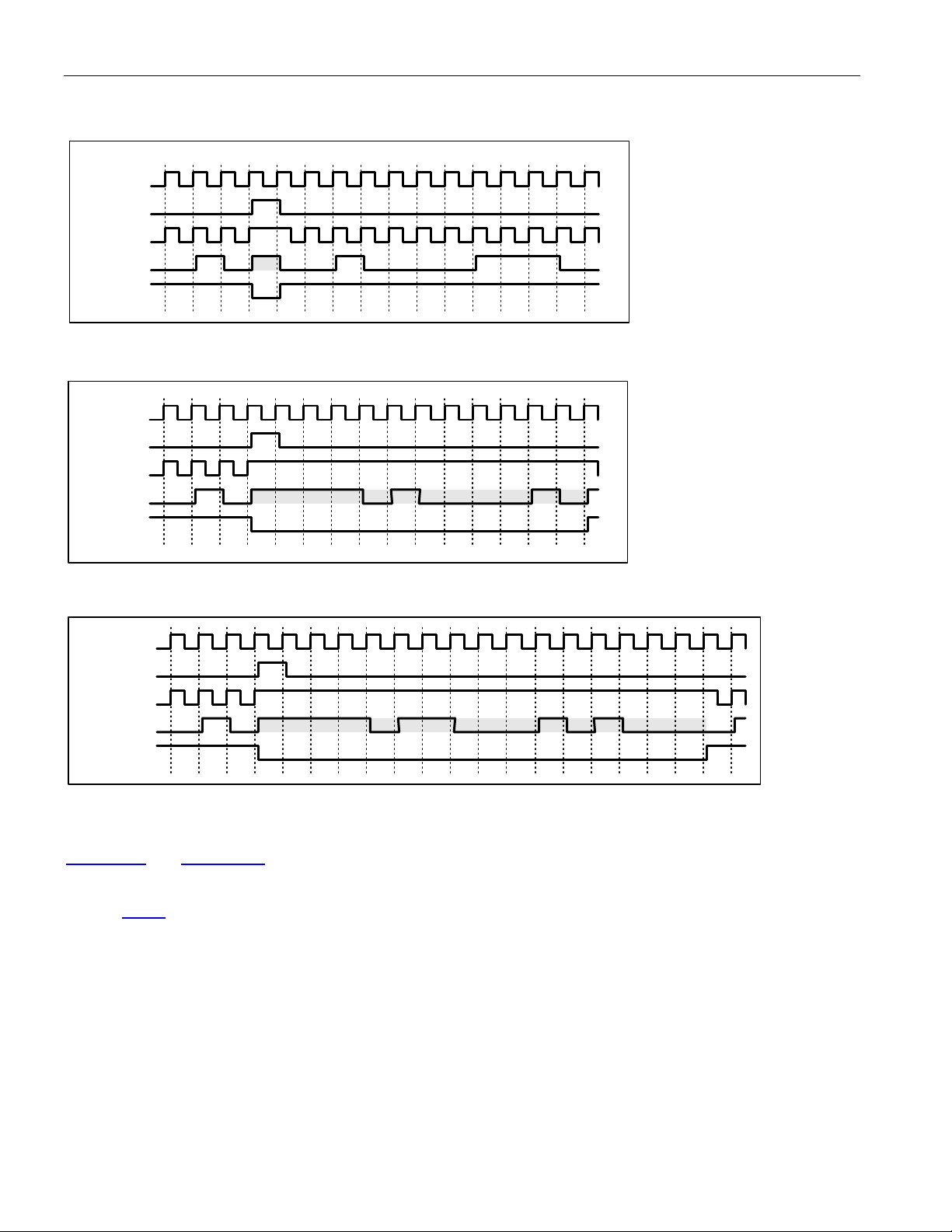
Figure 8-16. DS3 SCT Mode Receive Serial Interface Pin Timing
RCLKO or
RCLKI
RSOFO
DS3 RGCLK
DS3171/DS3172/DS3173/DS3174
DS3 RSER
DS3 RDEN
X1
6 7 8 9 10 11 12 1312345 1415
Figure 8-17. E3 G.751 SCT Mode Receive Serial Interface Pin Timing
RCLKO or
RCLKI
RSOFO
E3 RGCLK
E3 RSER
E3 RDEN
FAS 1111010000
6 7 8 9 10 11 12 1312345 1415
A
N
Figure 8-18. E3 G.832 SCT Mode Receive Serial Interface Pin Timing
RCLKO or
RCLKI
RSOF
E3 RGCLK
E3 RSER
FA1 11110110
FA2 00101000
E3 RDEN
6 7 8 9 10 11 12 131 2 3 4 5 14 15 16 17 18 19 20
8.3.4 Microprocessor Interface Functional Timing
Figure 8-19 and Figure 8-21 show examples of a 16-bit databus and an 8-bit databus, respectively. In 16-bit mode,
the A[0]/BSWAP signal controls whether or not to byte swap. In 8-bit mode, the A[0]/BSWAP signal is used as the
LSB of the address bus (A[0]). The selection of databus size is determined by the WIDTH input signal. See also
Section 10.1.1
.
42
Page 43

Figure 8-19. 16-Bit Mode Write
A[0]/BSWAP
DS3171/DS3172/DS3173/DS3174
A[10:1]
D[15:0]
CS
WR
RD
RDY
Note: Address 0x2B0 = 0x1234
0x2B0
0x1234
Z
Figure 8-20. 16-Bit Mode Read
A[0]/BSWAP
A[10:1]
D[15:0]
CS
0x2B0
0x1234
Z
WR
RD
RDY
Note: Address 0x2B0 = 0x1234
ZZ
43
Page 44

Figure 8-21. 8-Bit Mode Write
A[0]/BSWAP
DS3171/DS3172/DS3173/DS3174
A[10:1]
D[7:0]
CS
WR
RD
RDY
Note: Address 0x2B0 = 0x34
0x2B1 = 012
0x2B0
0x34
Z
Figure 8-22. 8-Bit Mode Read
A[0]/BSWAP
A[10:1]
D[7:0]
CS
0x2B0
0x34
0x2B0
0x12
Z
Z
Z
0x2B0
0x12
WR
RD
RDY
Note: Address 0x2B0 = 0x34
0x2B1 = 012
ZZ
ZZ
Figure 8-23
and Figure 8-24 are examples of databuses without and with byte swapping enabled, respectively.
When the A[0]/BSWAP pin is set to 0, byte swapping is disabled, and when one, byte swapping is enabled. This
pin should be static and not change while operating. Note: Address bit A[0] is not used in 16-bit mode. See also
Section 10.1.2
.
44
Page 45
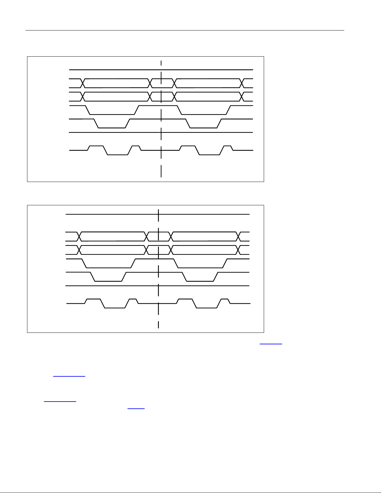
Figure 8-23. 16-Bit Mode without Byte Swap
A[0]/BSWAP
DS3171/DS3172/DS3173/DS3174
A[10:1]
D[15:0]
CS
WR
RD
RDY
Note: Address 0x2B0 = 0x1234
0x2B2 = 0x5678
0x2B0 0x2B2
0x1234 0x5678
Z
Z
Figure 8-24. 16-Bit Mode with Byte Swap
A[0]/BSWAP
A[10:1]
D[15:0]
CS
0x2B0
0x3412
Z
Z
0x2B2
0x7856
WR
RD
RDY
Note: Address 0x2B0 = 0x1234
0x2B2 = 0x5678
Z
Z
Z
Z
Clearing status latched registers on a read or write access is selectable via the GL.CR1
.LSBCRE register bit.
Clearing on read clears all bits in the register, while the clear on write clears only those bits which are written with a
‘1’ when the user writes to the status latched register.
To use the Clear on Read method, the user must only read the status latched register. All bits are set to zero after
the read. Figure 8-25
shows a read of a status latched register and another read of the same register verifying the
register has cleared.
To use the Clear on Write method, the user must write the register with ones in the bit locations that he desires to
clear. Figure 8-26
that he wrote a ‘1.’ See also Section 10.1.5
shows a read, a write, and then a subsequent read revealing the results of clearing of the bits
.
45
Page 46
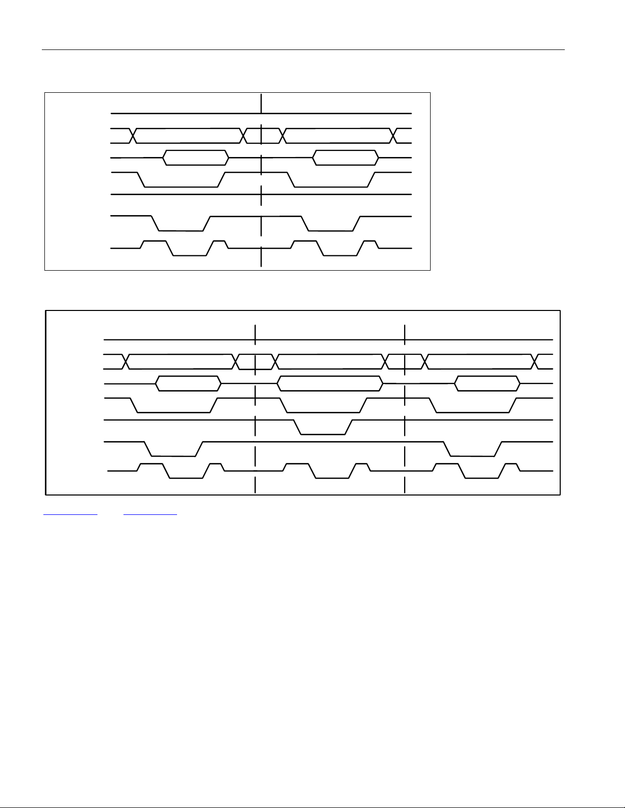
Figure 8-25. Clear Status Latched Register on Read
A[0]/BSWAP
DS3171/DS3172/DS3173/DS3174
A[10:1]
D[15:0]
CS
WR
RD
RDY
0x1C0
0xFFFF
Z
Z
Z
0x1C0
0x0000
Figure 8-26. Clear Status Latched Register on Write
A[0] /B SW AP
A[10: 1]
D[15:0]
CS
WR
0x1C0
0xFFFF
0x1C0
0x5555
Z
0x1C0
0xAAAA
RD
RDY
Figure 8-27
Z
Z
Z
and Figure 8-28show exaggerated views of the Ready Signal to describe the difference in access
Z
Z
Z
times to write or read to or from various memory locations on the DS317x device. Some registers will have a faster
access time than others will and if needed, the user can implement the RDY signal to maximize efficiency of read
and write accesses.
46
Page 47
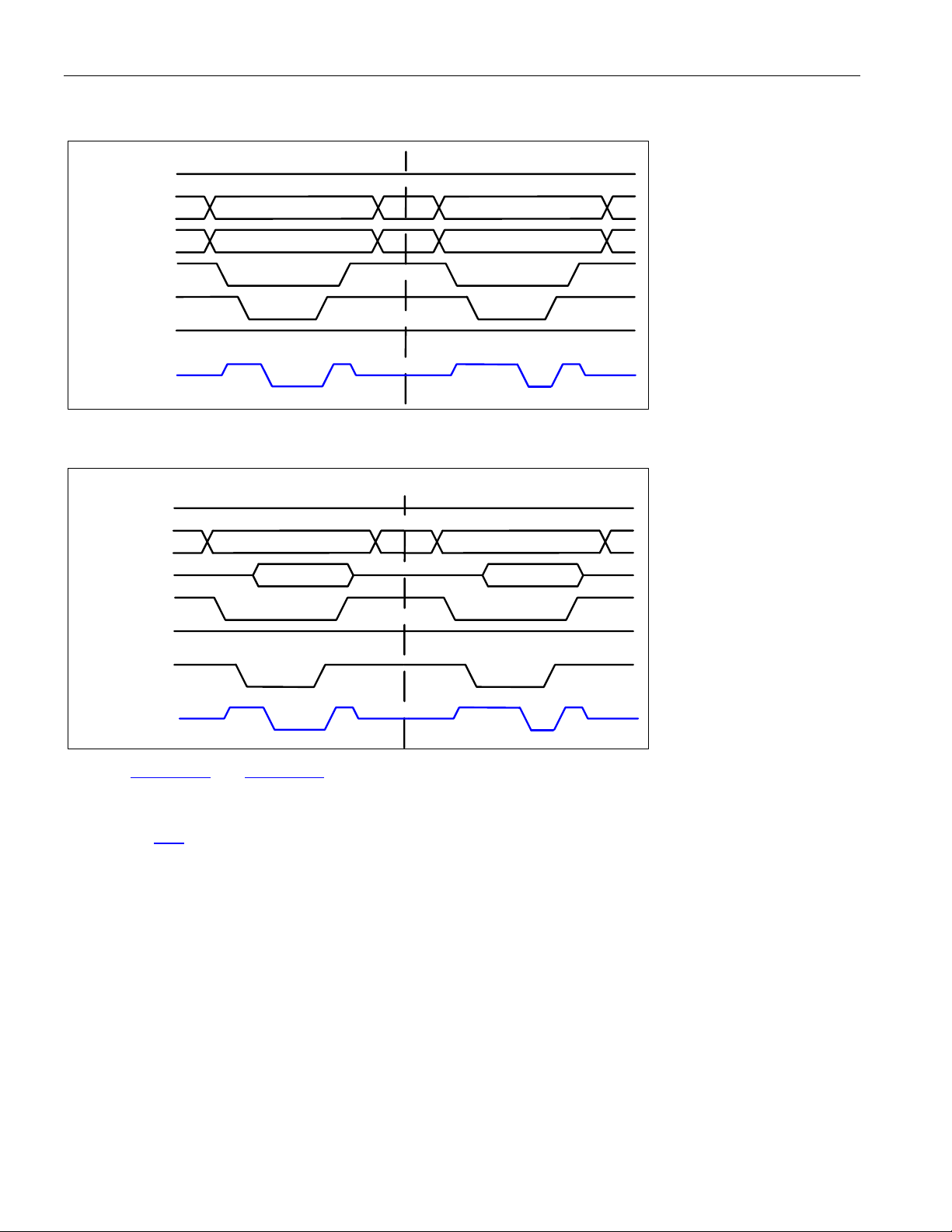
Figure 8-27. RDY Signal Functional Timing Write
A[0]/BSWAP
DS3171/DS3172/DS3173/DS3174
A[10:1]
D[15:0]
CS
WR
RD
RDY
0x2B0 0x3A4
0x1234 0x0078
Z
Z
Z
Figure 8-28. RDY Signal Functional Timing Read
A[0]/BSWAP
A[10:1]
D[15:0]
CS
WR
0x1C0
0xFFFF
0x3A4
Z
0xFFFF
RD
RDY
See also Figure 18-7
Z
and Figure 18-8.
8.3.5 JTAG Functional Timing
See Section 13.5.
Z
Z
Z
47
Page 48

DS3171/DS3172/DS3173/DS3174
9 INITIALIZATION AND CONFIGURATION
STEP 1: Check Device ID Code:
Before any testing can be done, device ID code, which is stored in GL.IDR, should be checked against device ID
codes shown below to ensure correct device is being used.
Current device ID codes are:
o DS3171 rev 1.0: 0044h
o DS3172 rev 1.0: 0045h
o DS3173 rev 1.0: 0046h
o DS3174 rev 1.0: 0047h
STEP 2: Initialize the Device.
Before configuring for operation, make sure the device is in a known condition with all registers set to their default
value by initiating a Global Reset (see Section 10.3
Global Reset bit (GL.CR1.RST). A Port Reset is not necessary since the global reset includes a reset of all ports to
their default values.
STEP 3: Clear the Reset.
). A Global Reset can be initiated via the RST pin or by the
It is necessary to clear the RST bit to begin normal operation.
After clearing the RST bit, the device is configured for default mode.
Default mode:
Framer: C-bit DS3
LIU: Disabled
STEP 4: Clear the Data Path Resets and the Port Power-Down bit.
The default value of the Data Path Resets is one, which keeps the internal logic in the reset status. The user needs
to clear the following bits:
GL.CR1.RSTDP = 0
PORT.CR1.RSTDP = 0
PORT.CR1.PD = 0
STEP 5: Configure the CLAD
If using the LIU, configure the CLAD (which supplies the clock to the Receive LIU) via the CLAD bits in
the GL.CR2
Note: The user must supply a DS3, E3, or STS-1 clock to the CLKA pin.
STEP 6: Select the clock source for the transmitter.
Loop Time (use the receive clock): Set PORT.CR3
CLAD Source: Set PORT.CR3.CLADC = 0
TCLKI Source: Set PORT.CR3
If using the CLAD, properly configure the CLAD by setting the CLAD bits in GL.CR2.
STEP 7: Configure the Framing Mode and the Line Mode..
PORT.CR2.LM[2:0] = 011 (LIU on, JA in Rx side) or another setting. See Table 10-26
PORT.CR2.FM[2:0] set to correct mode. See Table 10-25.
STEP 8: Disable Payload AIS (downstream AIS) and Line AIS
PORT.CR1.PAIS[2:0] = 111
PORT.CR1.LAIS[1:0] = 11
STEP 9: Enable each port (for non-LIU modes)
PORT.CR2.TLEN = 1
register.
.LOOPT = 1
.CLADC = 1
48
Page 49

DS3171/DS3172/DS3173/DS3174
Table 9-1. Configuration of Port Register Settings
Note: The Line Mode has been configured with the LIU enabled and the JA in the receive path (LM[2:0] = 011) for
all modes. Only Port 1 registers have been displayed.
Test the DS317x with the following configuration settings.
MODE PORT.CR1
0x040
DS3 C-Bit SCT 0x7C00 0000 0011 0000 0111 0x0000 0x0000
DS3 M13 SCT 0x7C00 0000 0011 0000 1111 0x0000 0x0000
E3.751 SCT 0x7C00 0000 0011 0001 0111 0x0000 0x0000
E3.823 SCT 0x7C00 0000 0011 0001 111X 0x0000 0x0000
Considerations
For best performance of the CLAD to meet jitter requirements across the temperature range, especially @ -40 C,
the following test registers should be set after reset:
Address 0x20B = 0x11
Address 0x20F = 0x11
PORT.CR2
0x042
PORT.CR3
0x044
PORT.CR4
0x046
9.1 Monitoring and Debugging
To determine if the device is receiving a good signal and that the chip is correctly configured for its environment,
check the following status registers.
Receive Loss of Lock – PORT.SR
from the incoming signal. This may indicate that the LIU’s master clock does not match the frequency of the
incoming signal. Verify that the CLAD is configured to match the clock input on the CLKA, CLKB, and CLKC pins
(DS3, E3, STS-1). See Table 10-11
.RLOL – The clock recovery circuit of the LIU was unable to recover the clock
.
Loss of Signal – LINE.RSR
there is no signal on the line, or that the signal is attenuated beyond recovery.
Loss of Frame – T3.RSR1
synchronize to the incoming data. Verify that the FM bits have been correctly configured for the correct mode of
traffic (DS3, E3 G.751, E3 G.832)
Other helpful techniques to utilize in diagnosing a problem include using Line Loopback and Diagnostic Loopback.
These features help to isolate and identify the source of the problem. Line Loopback will loop the receive input to
the transmit output, eliminating the transmit side input from the equation. Diagnostic Loopback will loop the transmit
output before the LIU to the receive framer, eliminating the analog Receive LIU and the receive side analog
circuitry.
One other potential problem is the Line Encoding/Decoding. The device needs to be configured in the same
mode as the far end piece of equipment. If the far end piece of equipment is transmitting and receiving HDB3/B3ZS
encoded data, the DS317x also must be configured to do the same. This is controlled by the LINE.TCR.TZSD and
the LINE.RCR.RZSD bits.
.LOS – This indicates that the LIU is unable to recover the clock and data because
.LOF (or E3751.RSR1 or E3832.RSR1) – This indicates that the framer was unable to
49
Page 50

DS3171/DS3172/DS3173/DS3174
10 FUNCTIONAL DESCRIPTION
10.1 Processor Bus Interface
10.1.1 8/16 Bit Bus Widths
The external processor bus can be sized for 8 or 16 bits using the WIDTH pin. When in 8-bit mode (WIDTH=0), the
address is composed of all the address bits including A[0], the lower 8 data lines D[7:0] are used and the upper 8
data lines D[15:8] are not used and never driven during a read cycle. When in 16-bit mode (WIDTH=1), the
address bus does not include A[0] (the LSB of the address bus is not routed to the chip) and all 16 data lines
D[15:0] are used. See Figure 8-19
10.1.2 Ready Signal (RDY)
The RDY signal allows the microprocessor to use the minimum bus cycle period for maximum efficiency. When this
signal goes low, the RD or WR cycle can be terminated. See Figure 8-27
NOTE: The RDY signal will not go active if the user attempts to read or write unused ports or unused registers not
assigned to any design blocks. The RDY signal will go active if the user writes or reads reserved registers or
unused registers within design blocks.
10.1.3 Byte Swap Modes
and Figure 8-21 for functional timing diagrams.
for functional timing diagrams.
The processor interface can operate in byte swap mode when the data bus is configured for 16-bit operation. The
A[0]/BSWAP pin is used to determine whether byte swapping is enabled. This pin should be static and not change
while operating. When the A[0]/BSWAP pin is low the upper register bits REG[15:8] are mapped to the upper
external data bus lines D[15:8], and the lower register bits REG[7:0] are mapped to the lower external data bus
lines D[7:0]. When the A[0]/BSWAP pin is high the upper register bits REG[15:8] are mapped to the lower external
data bus lines D[7:0], and the lower register bits REG[7:0] are mapped to the upper external data bus lines D[15:8].
See Figure 8-23
and Figure 8-24 for functional timing diagrams.
10.1.4 Read-Write / Data Strobe Modes
The processor interface can operate in either read-write strobe mode or data strobe mode. When MODE=0 the
read-write strobe mode is enabled and a negative pulse on RD performs a read cycle, and a negative pulse on WR
performs a write cycle. When MODE=1 the data strobe mode is enabled and a negative pulse on DS when R/W is
high performs a read cycle, and a negative pulse on DS when R/W is low performs a write cycle. The read-write
strobe mode is commonly called the “Intel” mode, and the data strobe mode is commonly called the “Motorola”
mode.
10.1.5 Clear on Read / Clear on Write Modes
The latched status register bits can be programmed to clear on a read access or clear on a write access. The
global control register bit GL.CR1.LSBCRE controls the mode that all of the latched registers are cleared. When
LSBCRE=0, the latched register bits will be cleared when the register is written to and the write data has the
register bits to clear set. When LSBCRE=1, the latched register bits that are set will be cleared when the register is
read.
The clear on write mode expects the user to use the following protocol:
1. Read the latched status register
2. Write to the registers with the bits set that need to be cleared.
This protocol is useful when multiple uncoordinated software tasks access the same latched register. Each task
should only clear the bits with which it is concerned; the other tasks will clear the bits with which they are
concerned.
50
Page 51

DS3171/DS3172/DS3173/DS3174
The clear on read mode is simpler since the bits that were read as being set will be cleared automatically. This
method will work well in a software system where multiple tasks do not read the same latched status register. The
latched status register bits in clear on read mode are carefully designed not to miss events that occur while a
register is being read when the latched bit has not already been set. Refer to Figure 8-25
and Figure 8-26.
10.1.6 Global Write Method
All of the ports can be written to simultaneously using the global write method. This method is enabled by setting
the GL.CR1
the same register on all valid ports. A valid port is a port that is available in a particular packaged part. For
example, port four would not be valid in a DS3173 device. After reset, the global write method is not enabled.
When the GWM bit is set, read data from the port registers is not valid and read data from the global and test
registers is valid. The data value read back from a port register should be ignored.
.GWM bit. When the global write method is enabled, a write to a register on any valid port will write to
10.1.7 Interrupt and Pin Modes
The interrupt (INT) pin is configurable to drive high or float when not active. The GL.CR1.INTM bit controls the pin
configuration, when it is set the INT pin will drive high when not active. After reset, the INT pin will be in high
impedance mode until an interrupt source is active and enabled to drive the interrupt pin.
10.1.8 Interrupt Structure
The interrupt structure is designed to efficiently guide the user to the source of an enabled interrupt source. The
status bits in the global status (GL.SR) and global status latched register (GL.SRL) are read to determine if the
interrupt source is a global event, a global performance monitor update or whether it came from one of the ports. If
the interrupt event came from one of the ports then the port status register (PORT.SR) and port status register
latched (PORT.SRL) can be read to determine if the interrupt source is a common port event like the performance
monitor update or LIU or whether it came from one of the DS3/E3 Framers, BERT, HDLC, FEAC or Trail Trace
status registers. If the interrupt came from one of the DS3/E3 Framers, BERT, HDLC, FEAC or Trail Trace status
registers, then one of those registers will need to be read to determine the event that caused the interrupt.
The source of an interrupt can be determined by reading three status registers: the global, port and block status
registers.
When a mode is not enabled, then interrupts from that source will not occur. For example, if E3 framing mode is
enabled, an interrupt source that is defined in DS3 framing, but not in E3 framing, cannot create a new interrupt.
Note that when modes are changed, the latched status bits of the new mode, as well as any other mode, may get
set. If the data path reset is set during or after the mode change, the latched status bits will be automatically
cleared. If the data path reset is not used to clear the latched status bits, then the registers must be cleared by
reading or writing to them based on the register clear method selected.
51
Page 52
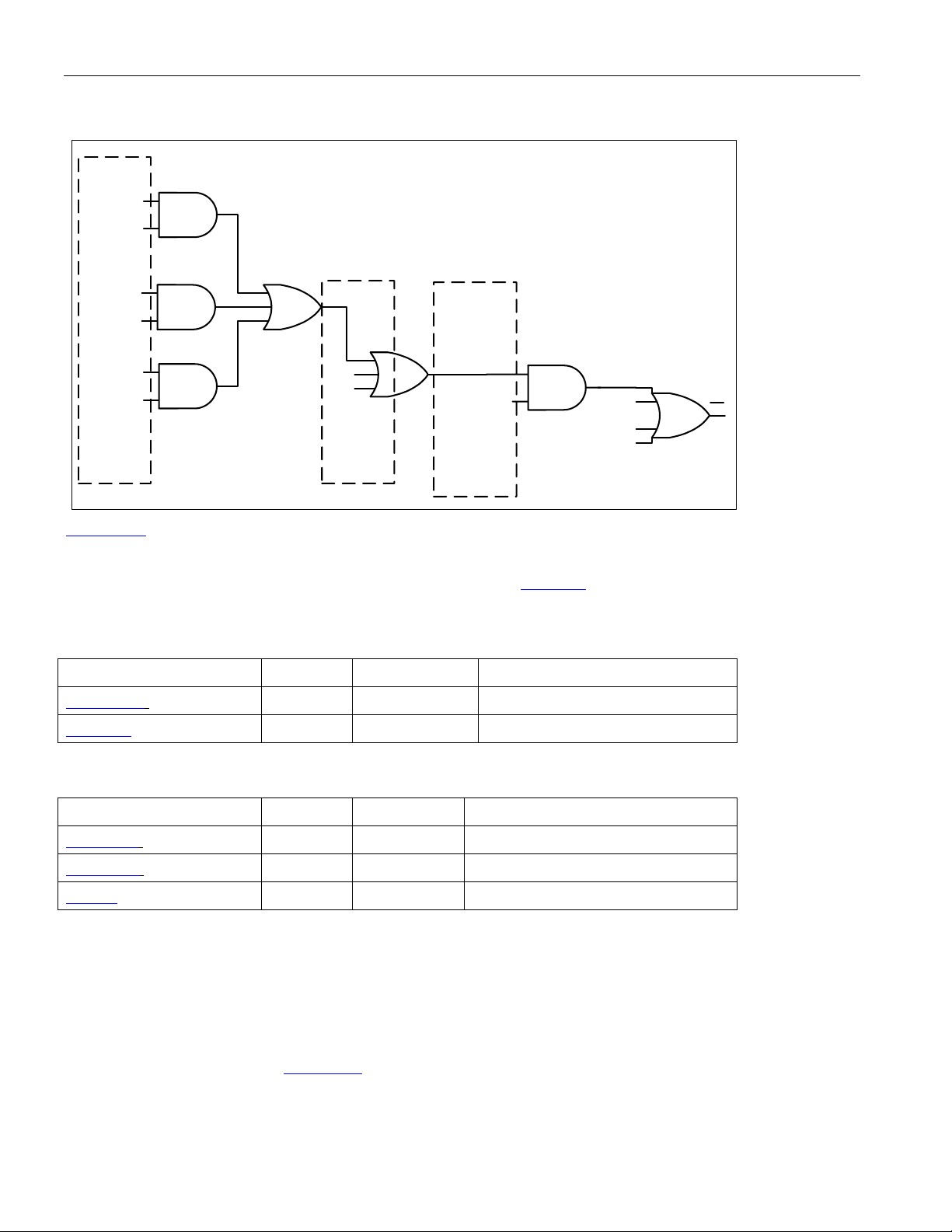
Figure 10-1. Interrupt Structure
SRL bit
SRIE bit
DS3171/DS3172/DS3173/DS3174
SRL bit
SRIE bit
SRL bit
SRIE bit
BLOCK LATCHED
STATUS and
INTERRUPT
ENABLE
REGISTERS
PORT.ISR bit
PORT INTERRUPT
STATUS
REGISTER
GL.ISR.PISRn
GL.ISRIE.
PISRIEn
GLOBAL
INTERRUPT
STATUS REGISTER
and INTERRUPT
ENABLE REGISTER
PORT
INTERRUPTS
GLOBAL
INTERRUPTS
INT
Figure 10-1
not only tells the user how to determine which event caused the interrupt, it also tells the user how to
enable a particular interrupt. Each block has a Status Register Interrupt Enable register that must be set in order to
enable an interrupt. The next step is to unmask the interrupt at the port level, on a per port basis. This is controlled
in the Global Interrupt Status Register Interrupt Enable register (GL.ISRIE
). Now the device is ready to drive the
INT pin low when a particular status bit gets set.
For example, in order to enable DS3 Out of Frame interrupts on Port 2, the following registers would need to be
written:
Register bit Address Value Written Note
T3.RSRIE1.OOFIE 0x2BC 0x0002 Unmask OOF interrupt on Port 2
GL.ISRIE.PISRIE2 0x010 0x0020 Unmask Port 2 interrupts
The following status registers bits will be set upon reception of OOF on Port 2:
Register bit Address Value Read Note
T3.RSRL1.OOFL 0x2B8 0x0002 DS3 Out of Frame on Port 2
PORT.ISR.FMSR 0x250 0x0001 Framer Block Interrupt Active, Port 2
GL.ISR.PISR2 0x010 0x0020 Port 2 Interrupt Active
10.2 Clocks
10.2.1 Line Clock Modes
10.2.1.1 Loop Timing Enabled
When loop timing is enabled (PORT.CR3
source. The TCLKIn pins are not used as a clock source. Because loop timing is enabled, the loopback functions
(LLB, PLB and DLB) do not cause the clock sources to switch when they are activated. The transmit and receive
.LOOPT), the transmit clock source is the same as the receive clock
52
Page 53

DS3171/DS3172/DS3173/DS3174
signal pins can be timed to a single clock reference without concern about having the clock source change during
loopbacks.
10.2.1.1.1 LIU Enabled, Loop Timing Enabled
In this mode, the receive LIU sources the clock for both the receive and transmit logic. The RCLKOn, TCLKOn and
TLCLKn clock output pins will be the same. The transmit or receive line payload signal pins can be timed to any of
these clock. The use of the RCLKOn pin as the timing source is suggested. If RCLKOn is used as the timing
source, be sure to set PORT.CR3
.RFTS = 0 for output timing.
10.2.1.1.2 LIU Disabled, Loop Timing Enabled
In this mode, the RLCLKn pins are the source of the clock for both the receive and transmit logic. The RCLKOn,
TCLKOn and TLCLKn clock output pins will both be the same as the RLCLKn clock. The transmit or receive line
payload signals can be timed to any of these clock pins. The use of the RLCLKn pin as the timing source is
suggested. If RLCLKn is used as the timing source, be sure to set PORT.CR3.RFTS = 1 for input timing.
10.2.1.2 Loop Timing Disabled
When loop timing is disabled, the transmit clock source can be different than the receive clock source. The
loopback functions, LLB, PLB and DLB, will cause the clock sources to switch when they are activated. Care must
be taken when selecting the clock reference for the transmit and receive signals.
The most versatile clocking option has the receive line interface signals timed to RLCLKn, the transmit line
interface signals timed to TLCLKn, the receive framer signals timed to RCLKOn, and the transmit framer signals
timed to TCLKOn. This clocking arrangement works in all modes.
When LLB is enabled, the clock on the TLCLKn pins will switch to the clock from the RLCLKn pins or RX LIU. It is
recommended that the transmit line interface signals be timed to the TLCLKn pins. If TLCLKn is used as the timing
source, be sure to set PORT.CR3
.TLTS = 0 for output timing.
When PLB is enabled, the TCLKIn pin will not be used and the internal transmit clock is switched to the internal
receive clock. The clock on the TCLKOn pins will switch to the clock from the RLCLKn pins or RX LIU. The framer
input signals will be ignored while PLB is enabled. It is recommended that the transmit line interface signals be
timed to the TCLKOn pins.
When DLB is enabled, the internal receive clock is switched to the internal transmit clock which is sourced from the
TCLKIn pins or one of the CLAD clocks, and the clock on the RLCLKn pins or from the RX LIU will not be used.
The clock on the RCLKOn pins will switch to the clock on the TCLKIn pins or one of the CLAD clocks. The receive
line signals from the RX LIU or line interface pins will be ignored. It is recommended that the receive framer pins be
timed to the RCLKOn pins. If TCLKOn is used as the timing source, be sure to set PORT.CR3
.TFTS = 0 for output
timing.
When both DLB and LLB are enabled, the TLCLKn clock pins are connected to either the RX LIU recovered clock
or the RLCLKn clock pins, and the RCLKOn clock pins will be connected to the TCLKIn clock pins or one of the
CLAD clocks. It is recommended that the transmit line signals be timed to the TLCLKn pins, the receive line
interface signals be timed to the RLCLKn pins, the receive framer signals be timed to the RCLKOn pins, and the
transmit framer signals be timed to the TCLKOn pins.
10.2.1.2.1 LIU Enabled - CLAD Timing Disabled – no LB
In this mode, the receive LIU sources the clock for the receive logic and the TCLKIn pins source the clock for the
transmit logic.
10.2.1.2.2 LIU Enabled - CLAD Timing Enabled – no LB
In this mode, the receive LIU sources the clock for the receive logic and one of the CLAD clocks sources the clock
for the transmit logic.
10.2.1.2.3 LIU Disabled - CLAD Timing Disabled – no LB
In this mode, the RLCLKn pins source the clock for the receive logic and the TCLKIn pins source the clock for the
transmit logic.
53
Page 54

DS3171/DS3172/DS3173/DS3174
10.2.1.2.4 LIU Disabled - CLAD Timing Enabled – no LB
In this mode, the RLCLKn pins source the clock for the receive logic and one of the CLAD clocks sources the clock
for the transmit logic.
10.2.2 Sources of Clock Output Pin Signals
The clock output pins can be sourced from many clock sources. The clock sources are the transmit input clocks
pins (TCLKIn), the receive clock input pins (RLCLKn), the recovered clock in the receive LIUs, and the clock
signals in the clock rate adapter circuit (CLAD). The default clock source for the receive logic is the RLCLKn pin if
the LIU is disabled; otherwise the default clock is sourced from the RX LIU clock when the RX LIU is enabled. The
default clock source for the transmit logic is the CLAD clocks.
The LIU is enabled based on the line mode bits(LM[2:0]) (See Table 10-26
and CLADC are located in the port configuration registers. LIUEN is not a register bit; it is a variable based on the
line mode bits. Table 10-1
decodes the LM bits for LiUEN selection.
). The bits LM[2:0], LBM[2:0], LOOPT
Table 10-1. LIU Enable Table
LM[2:0] LIUEN LIU Status
000 0 Disabled
001 1 Enabled
010 1 Enabled
011 1 Enabled
1XX 0 Disabled
Table 10-2 identifies the framer clock source and the line clock source depending on the mode that the device is
configured. Putting the device in loopback will typically mux in a different clock than the normal clock source.
Table 10-2. All Possible Clock Sources Based on Mode and Loopback
Rx FRAMER
MODE LOOPBACK
Loop Timed Any
Normal None
Normal LLB
Normal PLB
Normal DLB Same as Tx
Normal LLB and DLB Same as Tx
Table 10-3 identifies the source of the output signal TLCLKn based on certain variables and register bits.
CLOCK
SOURCE
RLCLKn or
RXLIU
RLCLKn or
RXLIU
RLCLKn or
RXLIU
RLCLKn or
RXLIU
Tx FRAMER
CLOCK
SOURCE
Same as Rx Same as Rx
TCLKIn or
CLAD
TCLKIn or
CLAD
Same as Rx Same as Rx
TCLKIn or
CLAD
TCLKIn or
CLAD
Tx LINE
CLOCK
SOURCE
Same as Tx
Same as Rx
Same as Tx
RLCLKn or
RXLIUn
54
Page 55

Table 10-3. Source Selection of TLCLK Clock Signal
DS3171/DS3172/DS3173/DS3174
Signal LOOPT
TLCLKn
Figure 10-2
PORT.
CR3
1 XXX NA 1 X RX LIU
1 XXX NA 0 X RLCLKn
0 010 LLB 1 X RX LIU
0 110 LLB 1 X RX LIU
0 010 LLB 0 X RLCLKn
0 110 LLB 0 X RLCLKn
0 011 PLB 1 X RX LIU
0 011 PLB 0 X RLCLKn
0 000 NO X 0 CLAD
0 001 NO X 0 CLAD
0 100 NO X 0 CLAD
0 10X NO X 0 CLAD
0 111 NO X 0 CLAD
0 000 NO X 1 TCLKIn
0 001 NO X 1 TCLKIn
0 100 NO X 1 TCLKIn
0 10X NO X 1 TCLKIn
0 111 NO X 1 TCLKIn
shows the source of the TCLKOn signals.
(PORT.CR4)
LBM[2:0]
LLB or
PLB
LIUEN CLADC
(PORT.
CR3)
Source
Figure 10-2. Internal TX Clock
PORT.CR3.
CLADC
CLAD
TCLKI
0
1
RCLKO
Table 10-4
identifies the source of the output signal TCLKOn based on certain variables and register bits.
PAYLOAD
LOOPBACK
0
TCLKO
1
55
Page 56

Table 10-4. Source Selection of TCLKOn (internal TX clock)
DS3171/DS3172/DS3173/DS3174
Signal LOOPT
PORT.CR3
TCLKOn
Figure 10-3
shows the source of the RCLKOn signals.
1 XXX 1 X RX LIU
1 XXX 0 X RLCLKn
0 PLB (011) 1 X RX LIU
0 PLB (011) 0 X RLCLKn
0 PLB disabled X 0 CLAD
0 PLB disabled X 1 TCLKIn
LBM[2:0] (PORT.CR4)
Figure 10-3. Internal RX Clock
LIUEN
RLCLK
0
LIUEN CLADC
DIAGNOSTIC
LOOPBACK
0
Source
(PORT.
CR3)
Rx LIU CLOCK
1
RCLKO
1
TCLKO
Table 10-5
identifies the source of the output signal RCLKOn based on certain variables and register bits.
Table 10-5. Source Selection of RCLKO Clock Signal (internal RX clock)
Signal LOOPT
PORT.CR3
RCLKOn
1 XXX 1 X RX LIU
1 XXX 0 X RLCLKn
0 DLB disabled 1 X RX LIU
0 DLB disabled & ALB
0 DLB (1XX) X 0 CLAD
0 DLB (1XX) or ALB
0 DLB (1XX) 1 1 TCLKIn
LBM[2:0]
(PORT.CR4)
disabled
(001)
LIUEN CLADC
(PORT.
CR3)
0 X RLCLKn
0 1 TCLKIn
Source
56
Page 57

DS3171/DS3172/DS3173/DS3174
10.2.3 Line IO Pin Timing Source Selection
The line IO pins can use any input clock pin (RLCLKn or TCLKIn) or output clock pin (TLCLKn, RCLKOn, or
TCLKOn) for its clock pin and meet the AC timing specifications as long as the clock signal is valid for the mode the
part is in. The clock select bit for the transmit line IO signal group PORT.CR3
output clock timing.
10.2.3.1 Transmit Line Interface Pins Timing Source Selection
(TPOSn/TDATn, TNEGn)
The transmit line interface signal pin group has the same functional timing clock source as the TLCLKn pin
described in Table 10-3
output pin is always a valid output clock for external logic to use for these signals when PORT.CR3
The transmit line timing select bit (TLTS) is used to select input or output clock pin timing. When TLTS=0, output
clock timing is selected. When TLTS=1, input clock timing is selected. If TLTS is set for input clock timing and an
output clock pin is used, or if TLTS is set for output clock timing and an input clock pin is used, then the setup, hold
and delay timings, as specified in Section 18.1
modes in which there is no input clock pin available for external timing since the clock source is derived internally
from the RX LIU or the CLAD.
. Other clock pins can be used for the external timing. The TLCLKn transmit line clock
will not be valid. There are some combinations of TLTS=1 and other
.TLTS selects the correct input or
.TLTS=0.
Table 10-6. Transmit Line Interface Signal Pin Valid Timing Source Select
LOOPT
1 XXX X X 0 TLCLKn, TCLKOn, RCLKOn
1 XXX 0 X 1 RLCLKn
1 XXX 1 X 1 No valid timing to any input clock pin
0 DLB (100) X X 0 TLCLKn, TCLKOn, RCLKOn
0 LLB (010) or PLB (011) X X 0 TLCLKn, RCLKOn
0 DLB&LLB (110) X X 0 TLCLKn
0 not DLB (100),
not LLB (010), not PLB (011)
and not LLB&DLB (110)
0 not LLB (010) and not PLB (011)
and not LLB&DLB (110)
0 not LLB (010) and not PLB (011)
and not LLB&DLB (110)
0 LLB (010) or PLB (011)
0 LLB (010) or PLB (011)
10.2.3.2 Transmit Framer Pin Timing Source Selection
(TSERn, TSOFIn, TSOFOn/TDENn)
LBM[2:0]
or DLB&LLB (110)
or DLB&LLB (110)
LIUEN
X X 0 TLCLKn, TCLKOn (default)
X 0 1 No valid timing to any input clock pin
X 1 1 TCLKIn
0 X 1 RLCLKn
1 X 1 No valid timing to any input clock pin
CLADC
Valid Timing to These Clock Pins
TLTS
The transmit framer signal pin group has the same functional timing clock source as the TCLKO pin described in
Table 10-4
valid output clock for external logic to use for these signals when TFTS=0.
The transmit framer select bit (TFTS) is used to select input or output clock pin timing. When TFTS=0, output clock
timing is selected. When TFTS=1, input clock timing is selected. If TFTS is set for input clock timing and an output
clock pin is used, or If TFTS is set for output clock timing and an input clock pin is used, then the setup, hold and
delay timings, as specified in Section 18.1
modes in which there is no input clock pin available for external timing since the clock source is derived internally
from the RX LIU or the CLAD.
. Other clock pins can be used for the external timing. The TCLKO transmit clock output pin is always a
will not be valid. There are some combinations of TFTS=1 and other
57
Page 58

Table 10-7. Transmit Framer Pin Signal Timing Source Select
DS3171/DS3172/DS3173/DS3174
LOOPT
1 XXX X X 0 TCLKOn, TLCLKn, RCLKOn
1 XXX 0 X 1 RLCLKn
1 XXX 1 X 1 No valid timing to any input clock pin
0 PLB (011) or DLB (100) or
0 PLB (011) or DLB (100) 1 X 0 TCLKOn, TLCLKn, RCLKOn
0 DLB&LLB (110) X X 0 TCLKOn, RCLKOn
0 LLB (010) X X 0 TCLKOn
0 not LLB, DLB or PLB (00X) X X 0 TCLKOn, TLCLKn
0 not PLB (011) X 0 1 No valid timing to any input clock pin
0 not PLB (011) X 1 1 TCLKIn
0 PLB (011) 0 X 1 RLCLKn
0 PLB (011) 1 X 1 No valid timing to any input clock pin
10.2.3.3 Receive Line Interface Pin Timing Source Selection
(RPOSn/RDATn, RNEGn/RLCVn)
The receive line interface signal pin group must clocked in with the RLCLK clock input pin. When the LIU is
enabled, the receive line interface pins are not used so there is no valid clock reference.
LBM[2:0]
ALB(001)
LIUEN
0 X 0 TCLKOn, TLCLKn, RCLKOn
CLADC
Valid Timing to These Clock Pins
TFTS
Table 10-8. Receive Line Interface Pin Signal Timing Source Select
LOOPT
X XXX 0 X RLCLKn
X XXX 1 X No valid timing to any clock pin
10.2.3.4 Receiver Framer Pin Timing Source Selection
(RSERn, RSOFOn/RDENn)
The receive framer signal pin group has the same functional timing clock source as the RCLKOn pin described in
Table 10-5
Other clock pins can be used for the external timing. The RCLKOn receive clock output pin is always a valid output
clock for external logic to use for these signals when PORT.CR3
The receive framer timing select bit (RFTS) is used to select input or output clock pin timing. When RFTS=0, output
clock timing is selected. When RFTS=1, input clock timing is selected. If RFTS is set for input clock timing and an
output clock pin is used, or If RFTS is set for output clock timing and an input clock pin is used, then the setup, hold
and delay timings, as specified in Section 18.1
other modes in which there is no input clock pin available for external timing since the clock source is derived
internally from the RX LIU or the CLAD.
.
LBM[2:0]
LIUEN
will not be valid. There are some combinations of RFTS=1 and
Valid Timing to These Clock Pins
CLADC
.RFTS=0.
58
Page 59

Table 10-9. Receive Framer Pin Signal Timing Source Select
DS3171/DS3172/DS3173/DS3174
LOOPT
1 XXX X X 0 RCLKOn, TLCLKn, TCLKOn
1 XXX 0 X 1 RLCLKn
1 XXX 1 X 1 No valid timing to any input clock pin
0 PLB (011) or DLB (100) or
0 PLB (011) or DLB (100) 1 X 0 RCLKOn, TLCLKn, TCLKOn
0 DLB&LLB (110) X X 0 RCLKOn, TCLKOn
0 LLB (010) X X 0 RCLKOn, TLCLKn
0 not LLB, DLB or PLB (00X) X X 0 RCLKOn
0 DLB (100) or LLB&DLB(110) X 0 1 No valid timing to any input clock pin
0 DLB (100) or LLB&DLB(110) X 1 1 TCLKIn
0 not DLB (100) and
0 not DLB (100) and
LBM[2:0]
ALB(001)
not LLB&DLB(110)
not LLB&DLB(110)
LIUEN
0 X 0 RCLKOn, TLCLKn, TCLKOn
0 X 1 RLCLKn
1 X 1 No valid timing to any input clock pin
CLADC
Valid Timing to These Clock Pins
RFTS
10.2.4 Clock Structures On Signal IO Pins
The signals on the input pins (TSOFIn, TSERn) can be used with any of the clock pins for setup/hold timing on
clock input and output pins. There will be a flop at each input whose clock is connected to the signal from the input
or output clock source pins with as little delay as possible from the signal on the clock IO pins. This means using
the input clock signal before the delays of the internal clock tree to clock the input signals, and using the output
clock signals used to drive the output clock pins to clock the input signals.
The signals on the output pins (TPOSn/TDATn, TNEGn, TSOFOn/TDENn, RSERn, RSOFOn/RDENn) can be with
any of the clock sources for delay timing. There will be a flop at each output whose clock is connected to the signal
from the input or output clock source pins with as little delay as possible from the signal on the clock IO pins. This
means using the input clock signal before the delays of the internal clock tree to clock the input signals, and using
the output clock signals used to drive the output clock pins to clock the input signals.
59
Page 60
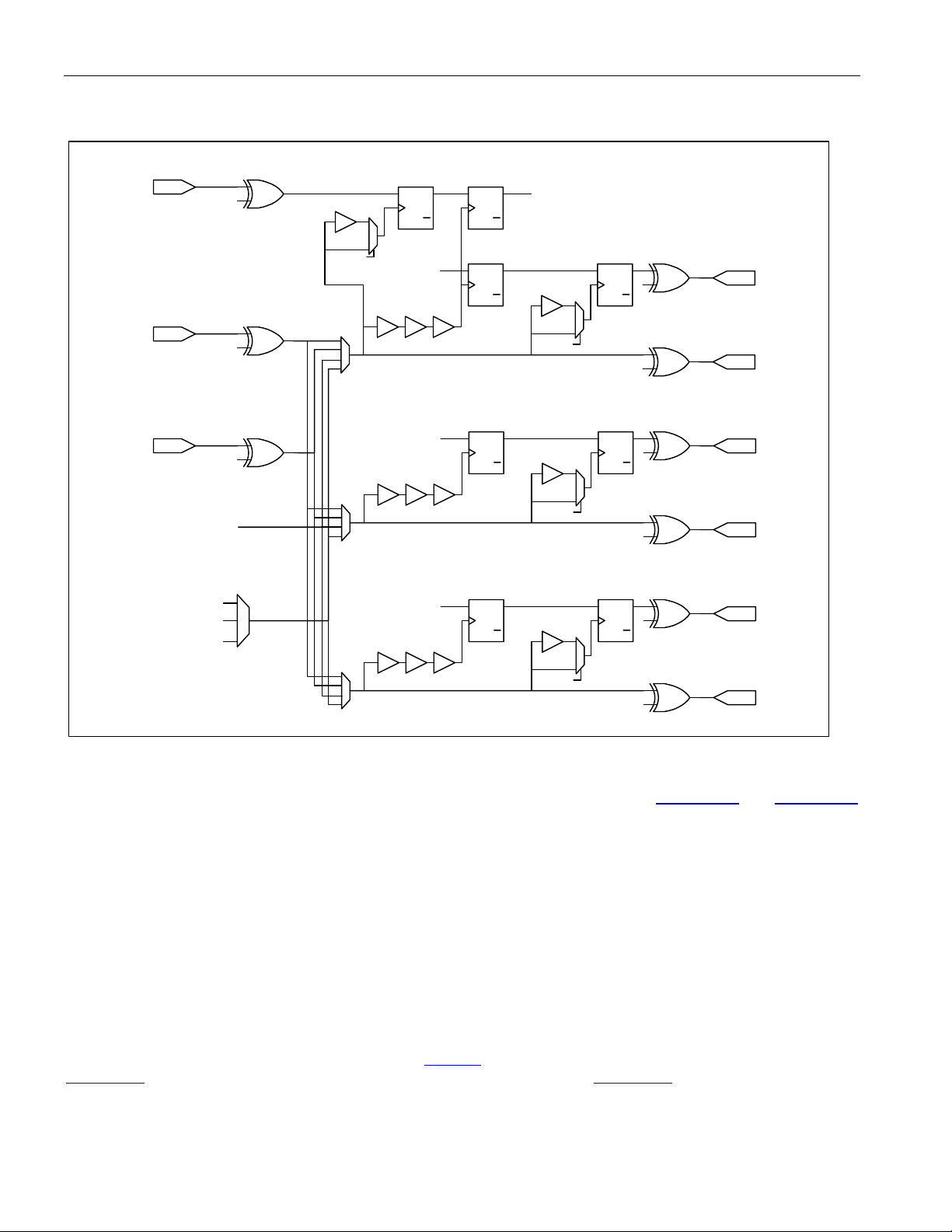
Figure 10-4. Example IO Pin Clock Muxing
DS3171/DS3172/DS3173/DS3174
TSER
PIN INVERT
TCLKI
PIN INVERT
RLCLK
PIN INVERT
RX LIU CLK
CLAD CLOCKS
DS3 CLK
E3 CLK
STS-1 CLK
DELAY
TFTS
SET
D
Q
0
1
Q
CLR
INTERNAL
SIGNAL
CLOCK TREE
INTERNAL
SIGNAL
CLOCK TREE
INTERNAL
SIGNAL
CLOCK TREE
Q
Q
Q
Q
INTERNAL
SIGNAL
DELAY
0
1
TFTS
SET
D
CLR
Q
Q
PIN INVERT
TDEN
TCLKO
SET
D
CLR
SET
D
CLR
PIN INVERT
SET
D
Q
DELAY
Q
CLR
SET
D
Q
Q
PIN INVERT
CLR
0
1
TLTS
TPOS
TLCLK
PIN INVERT
SET
D
Q
DELAY
Q
CLR
SET
D
Q
Q
PIN INVERT
CLR
0
1
RFTS
RSER
RCLKO
PIN INVERT
10.2.5 Gapped Clocks
The transmit and receive output clocks can be gapped in certain configurations. See Table 10-22 and Table 10-24
for the configuration settings. The gapped clocks are active during DS3 or E3 framed payload bits overhead bits
depending on which mode the device is configured for.
In the internal DS3 or E3 frame modes, the transmit gapped clock is created by the logical OR of the TCLKOn and
TDENn signals creating a positive or negative clock edge for each payload bit, the receive gapped clock is created
by the logical OR of the RCLKOn and RDENn signals.
When the output clock is disabled, the gapped output signal is high during clock periods if the pin is not inverted,
otherwise it will be low.
The gapped clocks are very useful when the data being clocked does not need to be aligned with any frame
structure. The data is simply clocked one bit at a time as a continuous data stream.
10.3 Reset and Power-Down
The device can be reset at a global level via the GL.CR1.RST bit or the RST pin and at the port level via the
PORT.CR1
reset using the power on reset signal from one of the LIUs as well as from the JTRST pin.
.RST bit and each port can be explicitly powered down via the PORT.CR1.PD bit. The JTAG logic is
60
Page 61
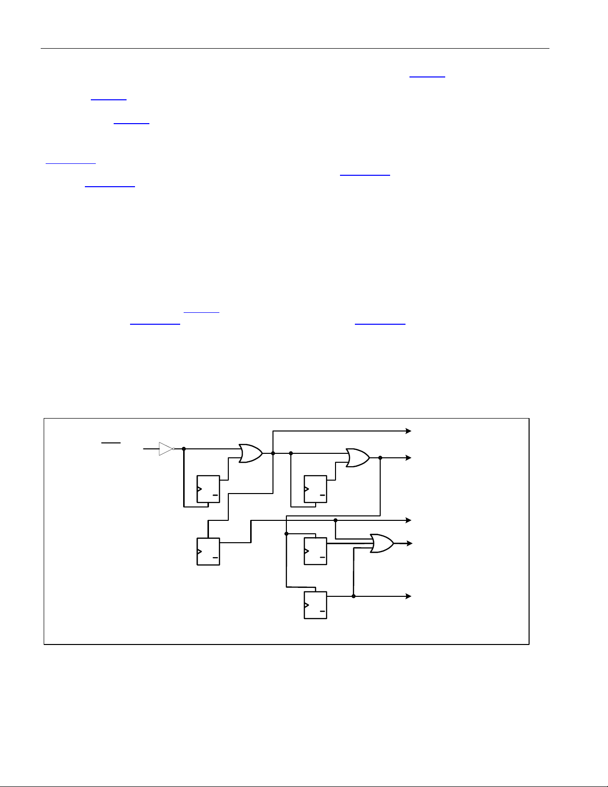
DS3171/DS3172/DS3173/DS3174
The external RST pin and the global reset bit in the global configuration register (GL.CR1
.RST) are combined to
create an internal global reset signal. The global reset signal resets all the status and control registers on the chip,
except the GL.CR1
.RST bit, to their default values and resets all the other flops in the global logic and ports to their
reset values. The processor bus output signals are also forced to be HIZ when the RST pin is active (low). The
global reset bit (GL.CR1
.RST) stays set after a one is written to it, but is reset to zero when the external RST pin is
active or when a zero is written to it.
At the port level, the global reset signal combines with the port-reset bit in the port control register
(PORT.CR1
the port to their default values and resets all the other flops, except PORT.CR1
.RST) to create a port-reset signal. The port reset signal resets all the status and control registers on
.RST, to their reset values. The port
reset bit (PORT.CR1.RST) stays set after a one is written to it, but is reset to zero when the global reset signal is
active or when a zero is written to it.
The data path reset function is a little different from the “general” reset function. The data path reset signal does not
reset the control register bits, but it does reset all of the status registers, counters and flops, the “general” reset
signal resets everything including the control register bits, excluding the reset bit. All clocks are functional, being
controlled by configuration bits, while data path reset is active. The LIU and CLAD circuits will be operating
normally during data path reset, which allows the internal phase locked loops to settle as quickly as possible. The
LIU will be sending all zeros (LOS) since data path reset will be forcing the transmit TPOSn and TNEGn to logic
zero. (NOTE: The BERT data path and control registers are reset when the global data path reset or the port data
path reset or the port power-down signal is active.)
The global data path reset bit (GL.CR1
.RSTDP) gets set to one when the global reset signal is active. The port
data path reset bit (PORT.CR1.RSTDP) and the port power-down bit (PORT.CR1.PD) bit get set to one when the
global reset signal is active or the port reset signal is active. These control bits will be cleared when a zero is
written to them if the global reset signal or the port-reset signal is not active. The global data path reset signal is
active when the global data path reset bit is set. The port data path reset signal is active when either the global
data path reset bit or the port data path reset bit is set. The port power-down signal is active when the port powerdown bit is set.
Figure 10-5. Reset Sources
Global Reset
RST pin
NOTE: Assumes
active high signals
SET
Q
D
GL.CR1. RST
Q
CLR
SET
Q
D
GL.CR1. RSTDP
Q
CLR
SET
Q
D
PORT.CR1.
Q
CLR
SET
Q
D
Q
CLR
PORT.CR1.
RSTDP
SET
Q
D
Q
CLR
PORT.CR1. PD
RST
Port Reset
Global Data Path Reset
Port Data Path Reset
Port Power Down
61
Page 62

DS3171/DS3172/DS3173/DS3174
Table 10-10. Reset and Power-Down Sources
Register bit states - F0: Forced to 0, F1: Forced to 1, 0: Set to 0, 1: Set to 1, X: Don’t care
Forced: Internally controlled
Set: User controlled
PIN REGISTER BITS INTERNAL SIGNALS
RST
0 F0 F1 F0 F1 F1 1 1 1 1 1
1 1 F1 F0 F1 F1 1 1 1 1 1
1 0 1 1 F1 F1 0 1 1 1 1
1 0 1 0 X 1 0 1 0 1 1
1 0 1 0 X 0 0 1 0 1 0
1 0 0 1 F1 F1 0 0 1 1 1
1 0 0 0 1 1 0 0 0 1 1
1 0 0 0 1 0 0 0 0 1 0
1 0 0 0 0 1 0 0 0 1 1
1 0 0 0 0 0 0 0 0 0 0
The reset signals in the device are asynchronous so they no not require a clock to put the logic into the reset state.
Clock signals may be needed to make the logic come out of the reset state.
The power-down function disables the appropriate clocks to cause the logic to generate a minimum of power. It
also puts the LIU circuits into the power-down mode. The 8KREF and ONESEC circuits can be powered down by
disabling the 8KREF source. The CLAD can also be powered down by disabling it.
After a global reset, all of the control and status registers in all ports are set to their default values and all the other
flops are reset to their reset values. The global register GL.CR1
and PORT.CR1.PD bits in all ports, are set after the global reset. A valid initialization sequence would be to clear
the PORT.CR1
desired modes, then clear the GL.CR1
ports to start up in a repeatable sequence. The device can also be initialized by clearing the GL.CR1.RSTDP,
PORT.CR1
modes, and clearing all of the latched status bits. The second initialization scheme could cause the device to
temporarily go into modes of operation that were not requested, but will quickly go into the requested modes of
operation.
G:RST
G:RSTDP
.PD bits in the ports that are to be active, write to all of the configuration registers to set them in the
.RSTDP and PORT.CR1.PD them writing to all of the configuration registers to set them in the desired
P:RST
P:RSTDP
P:PD
Global
reset
Global dp
reset
Port reset
.RSTDP, and the port register PORT.CR1.RSTDP
.RSTDP and PORT.CR1.RSTDP bits. This would cause the logic in the
Port dp
reset
Port power
dn
Some of the IO pins are put in a known state at reset. The transmit LIU outputs TXPn and TXNn are quiet and will
not drive positive or negative pulses. The global IO pins (GPIO[7:0]) are set as inputs at global reset. The port
output pins (TLCLKn, TPOSn/TDATn, TNEGn, TOHCLKn, TOHSOFn, TSOFOn/TDENn, TCLKOn/TGCLKn,
ROHn, ROHCLKn, ROHSOFn, RSERn, RSOFOn/RDENn, RCLKOn/RGCLKn) are driven low at global or port
reset and should stay low until after the port power-down PORT.CR1
PORT.CR1
inputs at global reset. The processor port tri-state output pins (D[15:0], RDY, INT) are forced into the high
impedance state when the RST pin is active, but not when the GL.CR1
After reset, the device will be in the default configuration:: The latched status bits are enabled to be cleared on
write. The CLAD is disabled. The global 8KREF and one-second timers are disabled. The line interface is in B3ZS
mode and the LIU is disabled and the transmit line pins are also disabled. The frame mode is DS3 C-bit with
automatic downstream AIS on LOS or OOF is enabled and automatic RDI on LOF, LOS, SEF or AIS is enabled
.RSTDP bits are cleared. The CLAD clock pins CLKA, CLKB and CLKC are the LIU reference clock
.RST bit is active.
62
.PD and port data path reset
Page 63

DS3171/DS3172/DS3173/DS3174
and automatic FEBE is enabled. Transmit clock comes from the CLAD CLKA pin. The pin inversion on all pins is
disabled.
Individual blocks are reset and powered down when not used determined by the settings in the line mode bits
PORT.CR2
.LM[2:0] and framer mode bits PORT.CR2.FM[2:0].
10.4 Global Resources
10.4.1 Clock Rate Adapter (CLAD)
The clock rate adapter is used to create multiple clocks for LIU reference clocks or transmit clocks from a single
clock reference input on the CLKA pin. The clock frequency applied to this pin must be at the DS3 (44.736 MHz),
E3 (34.368 MHz) and STS-1 (51.84 MHz) clock rates. Given one of these clocks the other two clocks will be
generated. The internally generated signals can be driven on output pins (CLKB and CLKC) for external use.
The receive LIU is supplied a reference clock from the CLAD. The receive LIU selects the clock frequency based
upon the mode the user selects via the FM bits. The CLAD output is also available as a transmit clock source if
selected via the PORT.CR2
The user must supply at least one of the three rates (DS3, E3, STS-1) to the CLKA pin. The CLAD[3:0] bits inform
the PLL of the frequency applied to the pins. Selection of the output clock of the CLAD applied to the LIU and
optionally the transmitter is controlled by the FM bits (located in PORT.CR2
to the user. The user may supply any of the three clock rates and use the CLAD to convert the rate to the particular
clock rate needed for his application.
.CLADC register bit.
). The CLAD allows maximum flexibility
Figure 10-6. CLAD Block
CLKA
CLKB
CLKC
DS3 clock
CLAD
E3 clock
CC52 clock
CLAD MODE
The clock rate adapter can also be disabled and all three clocks supplied externally using the CLKA, CLKB and
CLKC pins as clock inputs. When the CLAD is disabled, the three reference clocks DS3, E3 and STS-1 will need to
be applied to the CLKA, CLKB and CLKC pins, respectively. If any of the three frequencies is not required, it does
not need to be applied to the CLAD CLK pins.
63
Page 64

DS3171/DS3172/DS3173/DS3174
The CLAD MODE inputs to the clock rate adapter are composed of CLAD[3:0] control bits (located in the GL.CR2
Register) which determines which pins are input and output and which clock rate is on which pin. When
CLAD[3:0]=00XX, the PLL circuits are disabled and the signals on the input clock pins are used as the internal LIU
reference clocks. When CLAD[3:0]=(01XX or 10XX or 11XX), none, one or two PLL circuits are enabled to
generate the required clocks as determined by the CLAD[3:0] bits and the framing mode (FM[2:0]) and the line
mode (LM[2:0]) control bits. If a clock rate is not required on the CLAD output clock pins or for a reference clock for
any of the LIU, then the PLL used to generate that clock is disabled and powered down.
For example, in a design that only has the ports running at DS3 rates, then CLAD[3:0] can be set = 0100 and the
DS3 clock signal on the CLKA pin will be used as the DS3 LIU reference clock and no PLL circuit will be disabled.
Table 10-11. CLAD IO Pin Decode
GL.CR2.
CLAD[3:0]
00 XX DS3 clock input E3 clock input STS-1 clock input
01 00 DS3 clock input Low output Low output
01 01 DS3 clock input E3 clock output Low output
01 10 DS3 clock input Low output STS-1 clock output
01 11 DS3 clock input STS-1 clock output E3 clock output
10 00 E3 clock input Low output Low output
10 01 E3 clock input DS3 clock output Low output
10 10 E3 clock input Low output STS-1 clock output
10 11 E3 clock input STS-1 clock output DS3 clock output
11 00 STS-1 clock input Low output Low output
11 01 STS-1 clock input E3 output Low output
11 10 STS-1 clock input Low output DS3 clock output
11 11 STS-1 clock input DS3 clock output E3 clock output
CLKA PIN CLKB PIN CLKC PIN
10.4.2 8 kHz Reference Generation
The global 8KREF signal is used to generate the one-second-reference signal by dividing it by 8000. This signal
can be derived from almost any clock source on the chip as well as the general-purpose IO pin GPIO4. The port
8KREF signal can be sourced from either the global 8KREF signal or from the transmit or receive port clock or from
the receive 8KREF signal. The minimum input frequency stability of the 8KREF input pin is +/- 500 ppm.
The global 8KREF signal can come from an external 8000 Hz reference connected to the GPIO4 general-purpose
IO pin by setting the GL.CR2
pin when the GL.CR2
The global 8KREF signal can be derived from the CLAD PLL or pins or come from any of the port 8KREF signals
by clearing GL.CR2
The port 8KREF signal can be derived from the transmit clock input pin or from the receive LIU or input clock pin.
The PORT.CR3.
The 8KREF 8.000 kHz signal is a simple divisor of 44736 kHz (DS3 divided by 5592) or 33368 kHz (E3 divided by
4296). The correct divisor for the port 8KREF source is selected by the mode the port is configured for. The CLAD
clock chosen for the clock source selects the correct divisor for the global 8KREF. The 8KREF signal is only as
accurate as the clock source chosen to generate it.
Table 10-12
lists the selectable sources for global 8 kHz reference sources.
.G8KOS bit is set.
.G8KIS bit and selecting the source using the GL.CR2.G8KRS[2:0] bits.
P8KRS[1:0] bits are used to select which source.
.G8KIS bit. The global 8KREF signal can be output on the GPIO2 general-purpose IO
64
Page 65

Table 10-12. Global 8 kHz Reference Source Table
DS3171/DS3172/DS3173/DS3174
GL.CR2.
G8KIS
GL.CR2.
G8KRS[2:0]
Source
0 000 None, the 8KHZ divider is disabled.
0 001 Derived from CLAD DS3 clock output or CLKA pin if CLAD
is disabled. (Note: CLAD is disabled after reset)
0 010 Derived from CLAD E3 clock output or CLKB pin if CLAD is
disabled
0 011 Derived from CLAD STS-1 clock output or CLKC pin if CLAD
is disabled
0 100 Port 1 8KREF source selected by P8KRS[1:0]
0 101 Port 2 8KREF source selected by P8KRS[1:0]
0 110 Port 3 8KREF source selected by P8KRS[1:0]
0 111 Port 4 8KREF source selected by P8KRS[1:0]
1 XXX GPIO4 pin
Table 10-13
lists the selectable sources for port 8 kHz reference sources.
Table 10-13. Port 8 kHz Reference Source Table
PORT.CR3.P8KRS[1:0] Source
0X Undefined
10 Internal receive framer clock
11 Internal transmit framer clock
The 8 kHz reference logic tree is shown below.
Figure 10-7. 8KREF Logic
G8KRS[1:0]
FROM CLAD
DS3 CLK
E3 CLK
CC52 CLK
GPIO4
P8KRS
RX CLOCK
TX CLOCK
G8KRS[1:0]
0
1
CLOCK DIVIDER
1
2
3
OTHER
PORT
8KREF
CLOCK DIVIDER
0
1
2
3
G8KRS[2]
0
1
G8KREF
0
1
GLOBAL 8KREF
PORT 8KREF
FRAME MODE
65
Page 66

DS3171/DS3172/DS3173/DS3174
10.4.3 One Second Reference Generation
The one-second-reference signal is used as an option to update the performance registers on a precise onesecond interval. The generated internal signal should be about 50% duty cycle and it is derived from the Global 8
kHz reference signal by dividing it by 8000. The low to high edge on this signal will set the GL.SRL
one second detect bit which can generate an interrupt when the GL.SRIE.ONESIE interrupt enable bit is set. The
low to high edge can also be used to generate performance monitor updates when GL.CR1.GPM[1:0]=1X.
.ONESL latched
10.4.4 General-Purpose IO Pins
There are eight general-purpose IO pins that can be used for general IO, global signals and per port alarm signals.
Each pin is independently configurable to be a general-purpose input, general-purpose output, global signal or port
alarm. Two of the GPIO pins are assigned to each port and can be programmed to output one or two alarm
statuses using one or two GPIO pins. One of the two pins assigned to each port can be programmed as global
input or output signals. When the device is bonded out (or has ports powered down) to have 1, 2 or 3 ports active,
the GPIO pins associated with the disabled ports will still operate as either general-purpose inputs, generalpurpose outputs or global signals. When the ports are disabled and GL.GIOCR
be an output driving low. The 8KREFI, TMEI, and PMU signals that can be sourced by the GPIO pin will be driven
low into the core logic when the GPIO pin is not selected for the source of the signal.
.GPIOx[1:0] = 01, the GPIO pin will
Table 10-14
lists the purpose and control thereof of the General-Purpose IO Pins.
Table 10-14. GPIO Global Signals
Pin Global signal Control bit
GPIO2 8KREFO output GL.CR2.G8KOS
GPIO4 8KREFI input GL.CR2.G8KIS
GPIO6 TMEI input GL.CR1.MEIMS
GPIO8 PMU input GL.CR1.GPM[1:0]
Table 10-15 describes the selection of mode for the GPIO Pins.
Table 10-15. GPIO Pin Global Mode Select Bits
n = port 1 to 4, x = A or B, valid when a GPIO pin is not selected for a global signal
GL.GIOCR
.GPIOnSx
00 Input
01 Port alarm status selected by port
10 Output logic 0
11 Output logic 1
GPIO pin mode
GPIO
Table 10-16 lists the various port alarm monitors that can be output on the GPIO pins. The GPIO(A/B)[3:0] bits are
located in the PORT.CR4 Register.
66
Page 67

Table 10-16. GPIO Port Alarm Monitor Select
PORT.CR4
GPIO(A/B)[3:0]
LINE LOS
DS3/E3 OOF
DS3/E3 LOF
DS3/E3 AIS
DS3/E3 RAI
DS3 IDLE
0000 X
0001 X
0010 X
0011 X
0100 X
0101 X
0110
0111
1000
1001
1010
1011 X X X
1100
1101 X X X
1110 X X
1111 X X X X X X
DS3171/DS3172/DS3173/DS3174
10.4.5 Performance Monitor Counter Update Details
The performance monitor counters are designed to count at least one second of events before saturating to the
maximum count. There is a status bit associated with some of the performance monitor counters that is set when
the its counter is greater than zero, and a latched status bit that gets set when the counter changes from zero to
one. There is also a latched status bit that gets set on every event that causes the error counter to increment.
There is a read register for each performance monitor counter. The count value of the counter gets loaded into this
register and the counter is cleared when the update-clear operation is performed. If there is an event to be counted
at the exact moment (clock cycle) that the counter is to be cleared then the counter will be set to a value of one so
that that event will be counted.
The Performance Monitor Update signal affects the counter registers of the following blocks: the BERT, the DS3/E3
framer, the Line Encoder/Decoder.
The update-clear operation is controlled by the Performance Monitor Update signal (PMU). The update-clear
operation will update the error counter registers with the value of the error counter and also reset each counter.
The PMU signal can be created in hardware or software. The hardware sources can come from the one-second
counter or one of the general-purpose IO pins, which can be programmed to source this signal. The software
sources can come from one of the per-port control register bits or one of the global control register bits. When
using the software update method, the PMU control bit should be set to initiate the process and when the PMS
status bit gets set, the PMU control bit should be cleared making it ready for the next update. When using the
hardware update method, the PMS bit will be set shortly after the hardware signal goes high, and cleared shortly
after the hardware signal goes low. The latched PMS signal can be used to generate an interrupt for reading the
count registers. If the port is not configured for global PMU signals, the PMS signal from that port should be
blocked from affecting the global PMS status.
67
Page 68

Figure 10-8. Performance Monitor Update Logic
DS3171/DS3172/DS3173/DS3174
PORT.CR1.PMUM
PORT.CR1.PMU
GL.CR1.GPMU
GPIO8(GPMU) PIN
ONE SEC
GL.CR1.GPM
00
01
1X
other port counters
0
PMU PMS
1
PERF
COUNTER
GTZ
other ports
GL.SR.GPMS
PORT.SR.PMS
10.4.6 Transmit Manual Error Insertion
Transmit errors can be inserted in some of the functional blocks. These errors can be inserted using register bits in
the functional blocks, using the global GL.CR1.TMEI bit, using the port PORT.CR1.TMEI bit, or by using the GPIO6
pin configured for TMEI mode.
There is a transmit error insertion register in the functional blocks that allow error insertion. The MEIMS bit controls
whether the error is inserted using the bits in the error insertion register or using error insertion signals external to
that block. When bit MEIMS=0, errors are inserted using other bits in the transmit error insertion register. When bit
MEIMS=1, errors are inserted using a signal generated in the port or global control registers or using the external
GPIO6 pin configured for TMEI operation.
68
Page 69

Figure 10-9. Transmit Error Insert Logic
BERT.TEICR.MEIMS
DS3171/DS3172/DS3173/DS3174
PORT.CR.MEIMS
PORT.CR.TMEI
GL.CR1.MEIMS
GL.CR1.TMEI
GPIO6 PIN
(TMEI)
BERT.TEICR error
0
1
0
1
insertion bit
T3.TEIR error
insertion bit
0
BERT ERROR
INSERT
1
T3.TEIR.MEIMS
0
T3 ERROR
INSERT
1
0
1
10.5 Per Port Resources
10.5.1 Loopbacks
There are several loop back paths available. The following table lists the loopback modes available for analog
loopback (ALB), line loopback (LLB), payload loopback (PLB) and diagnostic loopback (DLB). The LBM bits are
located in PORT.CR4.
Table 10-17. Loopback Mode Selections
LBM[2:0] ALB LLB PLB DLB
000 0 0 0 0
001 1 0 0 0
010 0 1 0 0
011 0 0 1 0
10X 0 0 0 1
110 0 1 0 1
111 0 0 0 1
69
Page 70
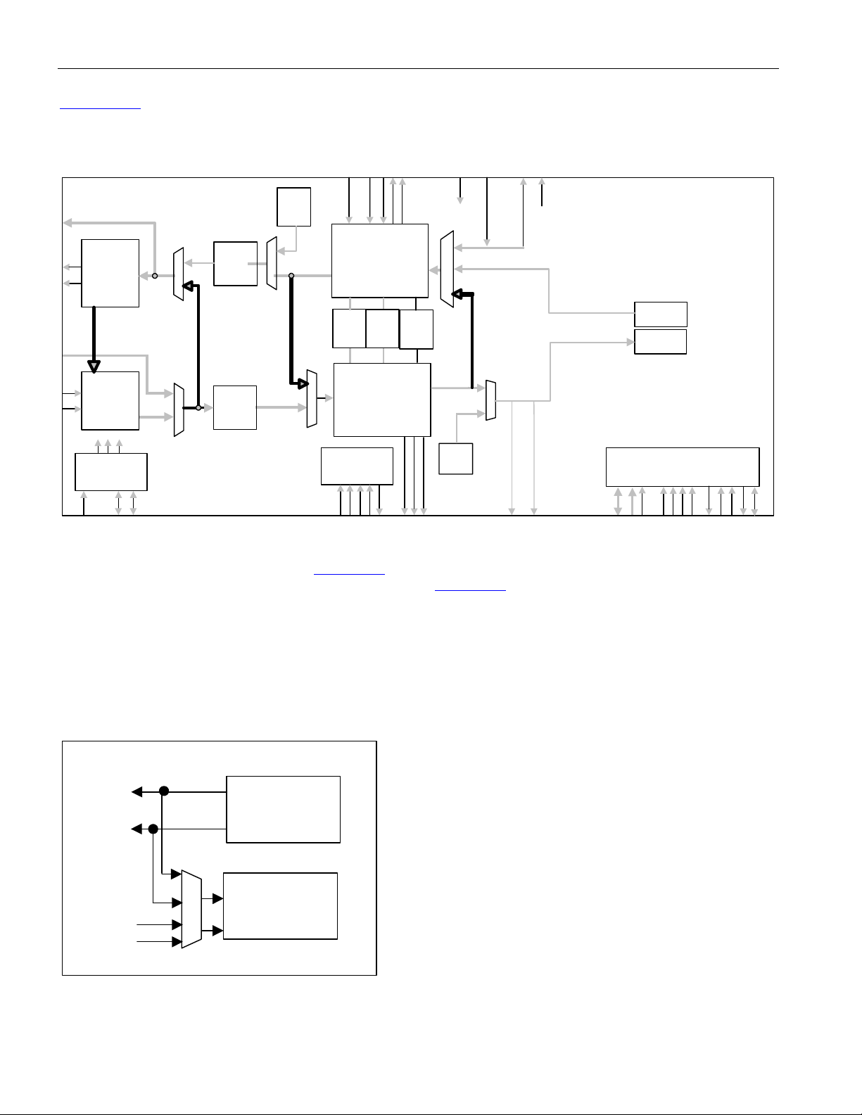
Figure 10-10
highlights where each loopback mode is located and gives an overall view of the various loopback
paths available.
Figure 10-10. Loopback Modes
TAIS
TUA1
DS3171/DS3172/DS3173/DS3174
DS3/E3
Transmit
LIU
ALB
DS3/E3
Receive
LIU
Clock Rate
Adapter
B3ZS/
HDB3
Encoder
LLB
B3ZS/
HDB3
Decoder
DLB
DS3 / E3
Transmit
Formatter
Trail
FEAC
Trace
Buffer
DS3 / E3
Receive
Framer
IEEE P1149.1
JTAG Test
Access Port
HDLC
UA1
GEN
TX BERT
PLB
RX BERT
Microprocessor
Interface
10.5.1.1 Analog Loopback (ALB)
Analog loopback is enabled by setting PORT.CR4
when the port is configured for loop-timed mode (set via the PORT.CR3
.LBM[2:0] = 001. Analog loopback mode will not be enabled
.LOOPT bit).
The analog loopback is a loopback as close to the pins as possible. When both the TX and RX LIU are enabled, it
loops back TXPn and TXNn to RXPn and RXNn, respectively. If the transmit signals on TXPn and TXNn are not
terminated properly, this loopback path may have data errors or loss of signal. When the LIU is not enabled, it
loops back TLCLKn,TPOSn / TDATn,TNEGn to RLCLKn, RPOSn / RDATn , RNEGn.
Figure 10-11. ALB Mux
TXP
TXN
RXP
RXN
TX
LIU
RX
LIU
70
Page 71

10.5.1.2 Line Loopback (LLB)
DS3171/DS3172/DS3173/DS3174
Line loopback is enabled by setting PORT.CR4
.LBM[2:0] = X10. DLB and LLB are enabled at the same time when
LBM[2:0] = 110, and only LLB is enabled when LBM[2:0] = 010.
The clock from the receive LIU or the RLCLKn pin will be output to the transmit LIU or TCLKOn pin. The POS and
NEG data from the receive LIU or the RPOSn and RNEGn pin will be sampled with the receive clock to time it to
the LIU or pin interface.
When LLB is enabled, unframed all ones AIS can optionally be automatically enabled on the receive data path.
This AIS signal will be output on the RSERn pin in SCT modes. When DLB and LLB are enabled, the AIS signal
will not be transmitted.
Refer to Figure 10-10
.
10.5.1.3 Payload Loopback (PLB)
Payload loopback is enabled by setting PORT.CR4
.LBM[2:0] = 011.
The payload loopback copies the payload data from the receive framer to the transmit framer which then re-frames
the payload before transmission. Payload loopback is operational in all framing modes.
When PLB is enabled, unframed all ones AIS transmission can optionally be automatically enabled on the receive
data path. This AIS signal will be output on the RSER. In all PLB modes, the TSOFIn input pin is ignored.
The external transmit output pins TDENn and TSOFOn/TDENn can optionally be disabled by forcing a zero when
PLB is enabled.
Refer to Figure 10-10
.
10.5.1.4 Diagnostic Loopback (DLB)
Diagnostic loopback is enabled by setting PORT.CR4
.LBM[2:0] = 1XX. DLB and LLB are enabled at the same time
when LBM[2:0] = 110, only DLB is enabled when LBM[2:0] = 10X or 111.
The Diagnostic loopback sends the transmit data, before line encoding, back to the receive side.
Transmit AIS can still be enabled using PORT.CR1
Refer to Figure 10-10
.
.LAIS[2:0] even when DLB is enabled.
10.5.2 Loss Of Signal Propagation
The Loss Of Signal (LOS) is detected in the line decoder logic. In unipolar (UNI) line interface modes LOS is never
detected. The LOS signal from the line decoder is sent to the DS3/E3 framer and the top-level payload AIS logic
except when DLB is activated. When DLB is activated the LOS signal to the framer and AIS logic is never active.
The LOS status in the line decoder status register is valid in all frame and loop back modes, though it is always off
in the line interface is in the UNI mode.
10.5.3 AIS Logic
There is AIS logic in both the framers and at the top-level logic of the ports. The framer AIS is enabled by setting
the TAIS bit in the appropriate framer transmit control register (T3, E3-G.751, E3-G.832, or Clear Channel). The
top level AIS is enabled by setting the PORT.CR1
all ones pattern or a DS3 framed 101010… pattern depending on the FM[2:0] mode bits. The DS3 Framed Alarm
Indication Signal (AIS) is a DS3 signal with valid F-bits, M-bits, and P-bits (P
set to one, all C-bits (CXY) are set to zero, and the payload bits are set to a 1010 pattern starting with a one
immediately after each overhead bit. The DS3 framed AIS pattern is only available in DS3 modes. The unframed all
ones pattern is available in all framing modes including the DS3 modes. The transmit line interface can send both
unframed all ones AIS and DS3 framed AIS patterns from either the AIS generator in the framer or the AIS
generator at the top level.
.LAIS[2:0] bits (see Table 10-18). The AIS signal is an unframed
1 and P2). The X-bits (X1 and X2) are
The AIS signal generated in the framer can be initiated and terminated without introducing any errors in the signal.
When the unframed AIS signal is initiated or terminated, there will be no BPV or CV errors introduced, but there will
71
Page 72

DS3171/DS3172/DS3173/DS3174
be framing errors if a framed mode is enabled. When the DS3 framed AIS signal is initiated or terminated, in
addition to no BPV or CV errors, there should be no framing or P-bit (parity) or CP-bit errors introduced.
The AIS signal generated at the top level will not generate BPV errors but may generate P-bit and CP-bit errors
when the signal is initiated and terminated. The framed DS3 AIS signal will not cause the far end receiver to resync when the signal is initiated, but it may cause a re-sync when terminated if the DS3 frame position in the
framer is changed while the DS3 AIS signal is being generated. A sequence of events can be executed which will
enable the initiation and termination of DS3 AIS or unframed all ones at the top level without any errors introduced.
The sequence will only work when the automatic AIS generation is not enabled. CV and P-bit errors can occur
when AIS is automatically generated and cannot be avoided. This sequence to generate an error free DS# AIS at
the top level is to have the DS3 AIS or unframed all ones signal initiate in the DS3 framer, and a few frames sent
before initiating or terminating the DS3 AIS or unframed all ones at the top level. After the top level AIS signal is
activated, the AIS signal in the framer can be terminated, DLB activated and diagnostic patterns generated. The
DS3 AIS signal generated at the top level will not change frame alignment after starting even if the DS3 frame
position in the framer is changed.
The transmit line AIS generator at the top level can generate AIS signals even when the framer is looped back
using DLB, but not when the line is looped back using LLB. The AIS signal generated in the framer will be looped
back to the receive side when DLB is activated.
The receive framer can detect both unframed all ones AIS and DS3 framed AIS patterns. When in DS3 framing
modes, both framed DS3 AIS and unframed all ones can be detected. In E3 framing modes E3 AIS, which is
unframed all ones, is detected.
The receive payload interface going to the RSERn pin or the BERT logic can have an unframed all ones AIS signal
replacing the receive signal, this is called Payload AIS. The all ones AIS signal is generated from either the DS3/E3
framer or the downstream top level unframed all ones AIS generator. The unframed all ones AIS signal generated
in the framer will be looped back to the transmit side when PLB is activated. The unframed all ones AIS signal
generated at the top level will be sent to the RSERn pin and other receive logic, but not to the transmit side while
PLB is activated. The top level AIS generator is used when a downstream AIS signal is desired while payload loop
back is activated and is enabled by default after rest and must be cleared during configuration. Note that the
downstream AIS circuit in the framer, when a DS3 mode is selected, enforces the OOF to be active for 2.5 ms
before activating when automatic AIS in the framer is enabled. The top level downstream AIS will be generated
with no delay when OOF is detected when automatic AIS at the top level is enabled.
There is no detection of any AIS signal on the transmit payload signal from the TSERn pin or anywhere on the
transmit data path.
The transmit AIS generator at the top level can also be activated with a software bit or automatically when DLB is
activated. The receive AIS generator in the framer can be activated with a software bit, and automatically when
AIS, LOS or OOF are detected. The receive payload AIS generator at the top level can be activated with a software
bit or automatically when LOS, DS3/E3 OOF, LLB or PLB is activated.
72
Page 73

Figure 10-12
shows the AIS signal flow through the device.
Figure 10-12. AIS Signal Flow
DS3171/DS3172/DS3173/DS3174
FRAMER
0
1
TAIS
DS3/UA1
AIS
detector
UA1
AIS
DS3/
UA1
AIS
TRANSMIT
LINE/TRIBUTARY
SIDE
Table 10-18
lists the LAIS decodes for various line AIS enable modes.
LINE
RECEIVE
LINE
LLB
optional
0
1
B3ZS/
HDB3
encoder
optional
B3ZS/
HDB3
decoder
0
1
TAIS
DS3/
UA1
AIS
TSOFO
1
0
DLB
Table 10-18. Line AIS Enable Modes
LAIS[1:0]
PORT.CR1
00 DS3 Automatic AIS when DLB is enabled
Frame Mode Description AIS Code
(PORT.CR4
.LBM = 1XX)
0
1
DAIS
0
1
PLB
UA1
AIS
DS3AIS
0
1
DAIS
TRANSMIT
PAYLOAD
SYSTEM/
TRUNK SIDE
RECEIVE
PAYLOAD
00 E3 Automatic AIS when DLB is enabled UA1
01 Any Send UA1 UA1
10 DS3 Send AIS DS3AIS
10 E3 Send AIS UA1
11 Any Disable none
73
Page 74

Table 10-19
lists the PAIS decodes for various payload AIS enable modes.
Table 10-19. Payload (Downstream) AIS Enable Modes
DS3171/DS3172/DS3173/DS3174
PAIS[2:0]
PORT.CR1
000 Always UA1
001 When LLB (no DLB) active UA1
010 When PLB active UA1
011 When LLB(no DLB) or PLB active UA1
100 When LOS (no DLB) active UA1
101 When OOF active UA1
110 When OOF, LOS. LLB (no DLB), or
111 Never none
When AIS is sent AIS Code
UA1
PLB active
10.5.4 Loop Timing Mode
Loop timing mode is enabled by setting the PORT.CR3.LOOPT bit. This mode replaces the clock from the TCLKIn
pin with the internal receive clock from either the RLCLKn pin if the RX LIU is disabled, or the recovered clock from
the RX LIU if it is enabled. The loop-timing mode can be activated in any framing or line interface mode.
10.5.5 HDLC Overhead Controller
The data signal to the receive HDLC controller will be forced to a one while still being clocked when the framer
(DS3, E3), to which the HDLC is connected, detects LOF or AIS. Forcing the data signal to all ones will cause an
HDLC packet abort if the data started to look like a packet instead of allowing a bad, and possibly very long, HDLC
packet.
10.5.6 Trail Trace
There is a single Trail Trace controller for use in line maintenance protocols. The E3-G.832 framer has access to
the trail trace controller.
10.5.7 BERT
There is a Bit Error Rate Test (BERT) circuit for each port for use in generating and detecting test signals in the
payload bits. The BERT can generate and detect PRBS patterns up to 2^32-1 bits as well as repeating patterns up
to 32 bits long. The generated BERT signal replaces the data on the TSERn pin in SCT modes when the BERT is
enabled by setting the PORT.CR1.BENA.
When the BERT is enabled The TDENn and RDENn pins will still be active but the data on the TSERn pin will be
discarded.
10.5.8 SCT port pins
The SCT port pins have multiple functions based on the framing mode the device is in as well as other pin mode
select bits.
10.5.8.1 Transmit SCT port pins
The transmit SCT pins are TSOFIn, TSERn, TSOFOn / TDENn, and TCLKOn / TGCLKn. They have different
functions based on the framing mode and other pin mode bits. Unused input pin functions should drive a logic zero
into the device circuits expecting a signal from that pin. The control bits that configure the pins’ modes are
PORT.CR2
.FM[2:0], PORT.CR3.TPFPE, PORT.CR3.TSOFOS and PORT.CR3.TCLKS.
74
Page 75

Table 10-20
multiplexed pins.
to Table 10-22 describe the function selected by the FM bits and other pin mode bits for the
Table 10-20. TSOFIn Input Pin Functions
DS3171/DS3172/DS3173/DS3174
FM[2:0] PORT.CR2
0XX (FSCT) TSOFIn
1XX (FBM) Not used
Pin function
Table 10-21. TSOFOn/TDENn/Output Pin Functions
FM[2:0] PORT.CR2
0XX (FSCT) 0 TDENn
0XX (FSCT) 1 TSOFOn
1XX (FBM) X Low
TSOFOS
PORT.CR3
Pin function
Table 10-22. TCLKOn/TGCLKn Output Pin Functions
FM[2:0]
PORT.CR2
0XX (FSCT) 0 TGCLKn TDENn
0XX (FSCT) 1 TCLKOn none
1XX (FBM) X TCLKOn none
10.5.8.2 Receive SCT port pins
TCLKS
PORT.CR3
Pin function Gap source
The receive SCT pins are RSERn, RSOFOn / RDENn and RCLKOn / RGCLKn. They have different functions
based on the framing mode and other pin mode bits. Unused input pin functions should drive a logic zero into the
device circuits expecting a signal from that pin. The control bits that configure these pins are PORT.CR2
PORT.CR3
Table 10-23
multiplexed pins.
.RPFPE, PORT.CR3.RSOFOS and PORT.CR3.RCLKS.
to Table 10-24 describe the function selected by the FM bits and other pin mode bits for the
.FM[2:0],
Table 10-23. RSOFOn/RDENn Output Pin Functions
FM[2:0]
PORT.CR2
0XX (FSCT) 0 RDENn
0XX (FSCT) 1 RSOFOn
1XX (CLR) X Low
1XX (CSCT) X High
RSOFOS
PORT.CR3
Pin function
75
Page 76
Table 10-24. RCLKOn/RGCLKn Output Pin Functions
DS3171/DS3172/DS3173/DS3174
FM[2:0]
PORT.CR2
0XX (FSCT) 0 RGCLKn RDENn
0XX (FSCT) 1 RCLKOn none
1XX (FBM) X RCLKOn none
RCLKS
PORT.CR3
Pin function Gap source
10.5.9 Framing Modes
The framing modes are selected independently of the line interface modes using the PORT.CR2.FM[2:0] control
bits. Different blocks are used in different framing modes. The bit error test (BERT) function can be enabled in any
mode. The LIU, JA and line encoder/decoder blocks are selected by the line mode (LM[2:0]) code.
Table 10-25. Framing Mode Select Bits FM[2:0]
FM[2:0] Description Line Code Figure
000 DS3 C-bit Framed B3ZS/AMI/UNI Figure 6-1
001 DS3 M13 Framed B3ZS/AMI/UNI Figure 6-1
010 E3 G.751 Framed HDB3/AMI/UNI Figure 6-1
011 E3 G.832 Framed HDB3/AMI/UNI Figure 6-1
100 DS3 Rate Clear Channel B3ZS/AMI/UNI Figure 6-2
11X E3 Rate Clear Channel HDB3/AMI/UNI Figure 6-2
10.5.10 Line Interface Modes
The line interface modes can be selected semi-independently of the framing modes using the PORT.CR2.LM[2:0]
control bits. The major blocks controlled are the transmit LIU (TX LIU), receive LIU (RX LIU), jitter attenuator (JA)
and the line encoder/decoder. The line encoder/decoder is used for B3ZS, HDB3 and AMI line interface encoding
modes. The line encoder-decoder block is not used for line encoding or decoding in the UNI mode but the BPV
counter in it can be used to count external pulses on the RNEGn / RCLVn pin. The jitter attenuator (JA) can be off
(OFF) or put in either the transmit (TX) or receive (RX) path with the TX LIU or RX LIU. Both TX LIU and RX LIU
can be enabled (ON) or disabled (OFF).
The “Analog Loop Back” (ALB) is available when the LIU is enabled or disabled. It is an actual loop back of the
analog positive and negative pulses from the TX LIU to the RX LIU when the LIU is enabled. If the LIU is disabled,
it is a digital loop back of the TLCLK, TPOS, TNEG signals to the RLCLK, RPOS and RNEG signals.
When the line is configured for B3ZS/HDB3/AMI line codes, the line codes are determined by the framing mode
and the TZCDS and RZCDS bits control the AMI line mode selection bits in the line encoder/decoder blocks. The
DS3 modes select the B3ZS line coding, the E3 modes select the HDB3 line codes. Refer to Table 10-26
configuration.
for
76
Page 77

Table 10-26. Line Mode Select Bits LM[2:0]
DS3171/DS3172/DS3173/DS3174
LINE.TCR.TZSD &
LINE.RCR.RZSD
0 000 B3ZS/HDB3 OFF OFF
0 001 B3ZS/HDB3 ON OFF
0 010 B3ZS/HDB3 ON TX
0 011 B3ZS/HDB3 ON RX
1 000 AMI OFF OFF
1 001 AMI ON OFF
1 010 AMI ON TX
1 011 AMI ON RX
X 1XX UNI OFF OFF
LM[2:0]
(PORT.CR2)
Line Code LIU JA
77
Page 78

DS3171/DS3172/DS3173/DS3174
10.6 DS3/E3 Framer / Formatter
10.6.1 General Description
The Receive DS3/E3 Framer receives a unipolar DS3/E3 signal, determines frame alignment and extracts the
DS3/E3 overhead in the receive direction. The Transmit DS3/E3 Formatter receives a DS3/E3 payload, generates
framing, inserts DS3/E3 overhead, and outputs a unipolar DS3/E3 signal in the transmit direction.
The Receive DS3/E3 Framer receives a DS3/E3 signal from the Receive LIU or RDATn (or RPOSn and RNEGn),
determines the frame alignment, extracts the DS3/E3 overhead, and outputs the payload with frame and overhead
The Transmit DS3/E3 Formatter receives a DS3/E3 payload on TSERn, generates a DS3/E3 frame, optionally
inserts DS3/E3 overhead, and transmits the DS3/E3 signal.
Refer to Figure 10-13
for the location of the DS3/E3 Framer/Formatter blocks in the DS3174, 3, 2, 1 devices.
Figure 10-13. Framer Detailed Block Diagram
TAIS
TUA1
DS3/E3
Transmit
LIU
ALB
DS3/E3
Receive
LIU
Clock Rate
Adapter
B3ZS/
HDB3
Encoder
LLB
B3ZS/
HDB3
Decoder
DLB
DS3 / E3
Transmit
Formatter
Trail
FEAC
Trace
Buffer
DS3 / E3
Receive
Framer
IEEE P1149.1
JTAG Test
Access Port
HDLC
UA1
GEN
PLB
TX BERT
RX BERT
Microprocessor
Interface
10.6.2 Features
10.6.2.1 Transmit Formatter
• Programmable DS3 or E3 formatter – Accepts a DS3 (M23 or C-bit) or E3 (G.751 or G.832) signal and
performs DS3/E3 overhead generation.
• Arbitrary framing format support – Generates a signal with an arbitrary framing format. The line
overhead/stuff periods are added into the data stream using an overhead mask signal.
• Generates alarms and errors – DS3 alarm conditions (AIS, RDI, and Idle) and errors (framing, parity, and
FEBE), or E3 alarm conditions (AIS and RDI/RAI) and errors (framing, parity, and REI) can be inserted into the
outgoing data stream.
• Externally controlled serial DS3/E3 overhead insertion port – Can insert all DS3 or E3 overhead via a
serial interface. DS3/E3 overhead insertion is fully controlled via the serial overhead interface.
• HDLC overhead insertion – An HDLC channel can be inserted into the DS3 or E3 data stream.
• FEAC insertion – A FEAC channel can be inserted into the DS3 or E3 data stream.
• Trail Trace insertion – Inputs and inserts the G.832 E3 TR byte.
78
Page 79

DS3171/DS3172/DS3173/DS3174
10.6.2.2 Receive Framer
• Programmable DS3 or E3 framer – Accepts a DS3 (M23 or C-bit) or E3 (G.751 or G.832) signal and performs
DS3/E3 overhead termination.
• Arbitrary framing format support – Accepts a signal with an arbitrary framing format. The Line overhead/stuff
periods are removed from the data stream using an overhead mask signal.
• Detects alarms and errors – Detects DS3 alarm conditions (SEF, OOMF, OOF, LOF, COFA, AIS, AIC, RDI,
and Idle) and errors (framing, parity, and FEBE), or E3 alarm conditions (OOF, LOF, COFA, AIS, and RDI/RAI)
and errors (framing, parity, and REI).
• Serial DS3/E3 overhead extraction port – Extracts all DS3 or E3 overhead and outputs it on a serial
interface.
• HDLC overhead extraction – An HDLC channel can be extracted from the DS3 or E3 data stream.
• FEAC extraction – A FEAC channel can be extracted from the DS3 or E3 data stream.
• Trail Trace extraction – Extracts and outputs the G.832 E3 TR byte.
10.6.3 Transmit Formatter
The Transmit Formatter receives a DS3 or E3 data stream and performs framing generation, error insertion,
overhead insertion, and AIS/Idle generation for C-bit DS3, M23 DS3, G.751 E3, or G.832 E3 framing protocols.
The bits in a byte are transmitted MSB first, LSB last. When they are input serially, they are input in the order they
are to be transmitted. The bits in a byte in an outgoing signal are numbered in the order they are transmitted, 1
(MSB) to 8 (LSB). However, when a byte is stored in a register, the MSB is stored in the highest numbered bit (7),
and the LSB is stored in the lowest numbered bit (0). This is to differentiate between a byte in a register and the
corresponding byte in a signal.
10.6.4 Receive Framer
The Receive Framer receives the incoming DS3, or E3, line/tributary data stream, performs appropriate framing,
and terminates and extracts the associated overhead bytes.
The Receive Framer processes a C-bit format DS3, M23 format DS3, G.751 format E3, or G.832 format E3 data
stream, performing framing, performance monitoring, overhead extraction, and generates downstream AIS, if
necessary.
The bits in a byte are received MSB first, LSB last. When they are output serially, they are output MSB first, LSB
last. The bits in a byte in an incoming signal are numbered in the order they are received, 1 (MSB) to 8 (LSB).
However, when a byte is stored in a register, the MSB is stored in the highest numbered bit (7), and the LSB is
stored in the lowest numbered bit (0). This is to differentiate between a byte in a register and the corresponding
byte in a signal.
Some bits, bit groups, or bytes (data) are integrated before being stored in a register. Integration requires the data
to have the same new data value for five consecutive occurrences before the new data value will be stored in the
data register. Unless stated otherwise, integrated data may have an associated unstable indication. Integrated data
is considered unstable if the received data value does not match the currently stored (integrated) data value or the
previously received data value for eight consecutive occurrences. The unstable condition is terminated when the
same value is received for five consecutive occurrences.
10.6.4.1.1 Receive DS3 Framing
DS3 framing determines the DS3 frame boundary. In order to identify the DS3 frame boundary, first the subframe
boundary must be found. The subframe boundary is found by identifying the subframe alignment bits F
and F
, which have a value of one, zero, zero, and one, respectively. See Figure 10-14. Once the subframe
X4
boundary is found, the multiframe frame boundary can be found. The multiframe boundary is found by identifying
the multiframe alignment bits M
, M2, and M3, which have a value of zero, one, and zero respectively. The DS3
1
framer is an off-line framer that only updates the data path frame counters when either an out of frame (OOF) or an
out of multiframe (OOMF) condition is present. The use of an off-line framer reduces the average time required to
reframe, and reduces data loss caused by burst error. The DS3 framer has a Maximum Average Reframe Time
(MART) of approximately 1.0 ms.
, FX2, FX3,
X1
79
Page 80

Figure 10-14. DS3 Frame Format
DS3171/DS3172/DS3173/DS3174
X
X
P
P
M
M
M
1
2
1
2
1
2
3
F
11
F
21
F
31
F
41
F
51
F
61
F
71
C
11
C
21
C
31
C
41
C
51
C
61
C
71
F
12
F
22
F
32
F
42
F
52
F
62
F
72
C
12
C
22
C
32
C
42
C
52
C
62
C
72
F
13
F
23
F
33
F
43
F
53
F
63
F
73
C
13
C
23
C
33
C
43
C
53
C
63
C
73
F
14
F
24
F
34
F
44
F
54
F
64
F
74
7 SubFrames
680 Bits
The subframe framer continually searches four adjacent bit positions for a subframe boundary. A subframe
alignment bit (F-bit) checker checks each bit position. All four bit positions must fail before any other bit positions
are checked for a subframe boundary. There are 170 possible bit positions that must be checked, and four
positions are checked simultaneously. Therefore up to 43 checks may be needed to identify the subframe
boundary. The subframe framer enables the multiframe frame once it has identified a subframe boundary. Refer to
Figure 10-15
for the subframe framer state diagram.
Figure 10-15. DS3 Subframe Framer State Diagram
Sync
A
l
l
r
o
d
e
l
i
a
f
s
n
o
e
i
t
v
i
s
s
t
o
i
p
b
-
t
i
F
b
6
3
1
All 4 bit positions failed
d
e
i
f
i
r
4
b
i
t
p
o
s
i
t
i
o
n
s
f
a
i
l
e
d
LoadVerify
2 F-bits loaded
80
Page 81
DS3171/DS3172/DS3173/DS3174
The multiframe framer checks for a multiframe boundary. When the multiframe framer identifies a multiframe
boundary, it updates the data path frame counters if either an OOF or OOMF condition is present. The multiframe
framer waits until a subframe boundary has been identified. Then, each bit position is checked for the multiframe
boundary. The multiframe boundary is found by identifying the three multiframe alignment bits (M-bits). Since there
are seven multiframe bits and three bits are required to identify the multiframe boundary, up to 9 checks may be
needed to find the multiframe boundary. Once the multiframe boundary is identified, it is checked in each
subsequent frame. The data path frame counters are updated if the three multiframe alignment bits are error free,
and an OOF or OOMF condition exists. If the multiframe framer checks more than fifteen multiframe bit (X-bits, Pbits, and M-bits) positions without identifying the multiframe boundary, the multiframe framer times out, and forces
the subframe framer back into the load state. Refer to Figure 10-16 for the multiframe framer state diagram.
10.6.4.1.2 Receive DS3 Performance Monitoring
Performance monitoring checks the DS3 frame for alarm conditions and errors. The alarm conditions detected are
OOMF, OOF, SEF, LOF, COFA, LOS, AIS, Idle, RUA1, and RDI. The errors accumulated are framing, P-bit parity,
C-bit parity (C-bit format only), and Far-End Block Error (FEBE) (C-bit format only) errors.
An Out Of MultiFrame (OOMF) condition is declared when a multiframe alignment bit (M-bit) error has been
detected in two or more of the last four consecutive DS3 frames, or when a manual resynchronization is requested.
An OOMF condition is terminated when no M-bit errors have been detected in the last four consecutive DS3
frames, or when the DS3 framer updates the data path frame counters. Figure 10-16 shows the multiframe framer
state diagram.
Figure 10-16. DS3 Multiframe Framer State Diagram
Sync
M
-
b
i
d
e
i
f
i
t
n
e
d
i
s
t
i
b
-
M
r
o
r
r
e
t
i
b
-
M
Timeout
t
e
r
r
o
r
a
n
d
t
i
m
e
o
u
t
LoadVerify
2 multiframe loaded
If multiframe alignment OOF is disabled, an Out Of Frame (OOF) condition is declared when three or more out of
the last sixteen consecutive subframe alignment bits (F-bits) have been errored, or a manual resynchronization is
requested. If multiframe alignment OOF is enabled, an OOF condition is declared when three or more out of the
last sixteen consecutive F-bits have been errored, when an OOMF condition is declared, or when a manual
resynchronization is requested. If multiframe alignment OOF is disabled, an OOF condition is terminated when
none of the last sixteen consecutive F-bits has been errored, or when the DS3 framer updates the data path frame
counters. If multiframe alignment OOF is enabled, an OOF condition is terminated when an OOMF condition is not
81
Page 82

DS3171/DS3172/DS3173/DS3174
active and none of the last sixteen consecutive F-bits has been errored, or when the DS3 framer updates the data
path frame counters. Multiframe alignment OOF is programmable (on or off).
A Severely Errored Frame (SEF) condition is declared when three or more out of the last sixteen consecutive F-bits
have been errored, or when a manual resynchronization is requested. An SEF condition is terminated when an
OOF condition is absent.
A Loss Of Frame (LOF) condition is declared by the LOF integration counter when it has been active for a total of T
ms. The LOF integration counter is active (increments count) when an OOF condition is present, it is inactive (holds
count) when an OOF condition is absent, and it is reset when an OOF condition is absent for T continuous ms. T is
programmable (0, 1, 2, or 3). An LOF condition is terminated when an OOF condition is absent for T continuous
ms.
A Change Of Frame Alignment (COFA) is declared when the DS3 framer updates the data path frame counters
with a frame alignment that is different from the current data path DS3 frame alignment.
A Loss Of Signal (LOS) condition is declared when the B3ZS encoder is active, and it declares an LOS condition.
An LOS condition is terminated when the B3ZS encoder is inactive, or it terminates an LOS condition.
An Alarm Indication Signal (AIS) is a DS3 signal with valid F-bits and M-bits. The X-bits (X
the P-bits (P
and P2) are set to zero, all C-bits (CXY) are set to zero, and the payload bits are set to a 1010 pattern
1
and X2) are set to one,
1
starting with a one immediately after each DS3 overhead bit. An AIS signal is present when a DS3 frame is
received with valid F-bits and M-bits, both X-bits set to one, both P-bits set to zero, all C-bits set to zero, and all but
seven or fewer payload data bits matching the DS3 overhead aligned 1010 pattern. An AIS signal is absent when a
DS3 frame is received that does not meet the aforementioned criteria for an AIS signal being present. The AIS
integration counter declares an AIS condition when it has been active for a total of 10 to 17 DS3 frames. The AIS
integration counter is active (increments count) when an AIS signal is present, it is inactive (holds count) when an
AIS signal is absent, and it is reset when an AIS signal is absent for 10 to 17 consecutive DS3 frames. An AIS
condition is terminated when an AIS signal is absent for 10 to 17 consecutive DS3 frames.
A Receive Unframed All 1’s (RUA1) condition is declared if in each of 4 consecutive 2047 bit windows, five or less
zeros are detected and an OOF condition is continuously present . A RUA1 condition is terminated if in each of 4
consecutive 2047 bit windows, six or more zeros are detected or an OOF condition is continuously absent.
An Idle Signal (Idle) is a DS3 signal with valid F-bits, M-bits, and P-bits (P
to one, C
, C32, and C33 are set to zero, and the payload bits are set to a 1100 pattern starting with 11 immediately
31
and P2). The X-bits (X1 and X2) are set
1
after each overhead bit. In C-bit mode, an Idle signal is present when a DS3 frame is received with valid F-bits, Mbits, and P-bits, both X-bits set to one, C
, C32, and C33 set to zero, and all but seven or fewer payload data bits
31
matching the T3 overhead aligned 1100 pattern. In M23 mode, an Idle signal is present when a T3 frame is
received with valid F-bits, M-bits, and P-bits, both X-bits set to one, and all but seven or fewer payload data bits
matching the overhead aligned 1100 pattern. An Idle signal is absent when a DS3 frame is received that does not
meet aforementioned criteria for an Idle signal being present. The Idle integration counter declares an Idle
condition when it has been active for a total of 10 to 17 DS3 frames. The Idle integration counter is active
(increments count) when an Idle signal is present, it is inactive (holds count) when an Idle signal is absent, and it is
reset when an Idle signal is absent for 10 to 17 consecutive DS3 frames. An Idle condition is terminated when an
Idle signal is absent for 10 to 17 consecutive DS3 frames.
A Remote Defect Indication (RDI) condition (also called a far-end SEF/AIS defect condition) is declared when four
consecutive DS3 frames are received with the X-bits (X
and X2) set to zero. An RDI condition is terminated when
1
four consecutive DS3 frames are received with the X-bits set to one.
A DS3 Framing Format Mismatch (DS3FM) condition is declared when the DS3 format programmed (M13, C-bit)
does not match the incoming DS3 signal framing format. A DS3FM condition is terminated when the incoming DS3
signal framing format is the same format as programmed. Framing errors are determined by comparing F-bits and
M-bits to their expected values. The type of framing errors accumulated is programmable (OOFs, F & M, F, or M).
An OOF error increments the count whenever an OOF condition is first detected . An F & M error increments the
count once for each F-bit or M-bit that does not match its expected value (up to 31 per DS3 frame). An F error
increments the count once for each F-bit that does not match its expected value (up to 28 per DS3 frame). An M
error increments the count once for each M-bit that does not match its expected value (up to 3 per DS3 frame).
82
Page 83

DS3171/DS3172/DS3173/DS3174
P-bit parity errors are determined by calculating the parity of the current DS3 frame (payload bits only), and
comparing the calculated parity to the P-bits (P
match P
or P2, a single P-bit parity error is declared.
1
and P2) in the next DS3 frame. If the calculated parity does not
1
C-bit parity errors (C-bit format only) are determined by calculating the parity of the current DS3 frame (payload bits
only), and comparing the calculated parity to the C-bits in subframe three (C
If the calculated parity does not match C
, C32, or C33, a single C-bit parity error is declared.
31
FEBE errors (C-bit format only) are determined by the C-bits in subframe four (C
, C32, and C33) in the next DS3 frame.
31
, C42, and C43). A value of 111
41
indicates no error and any other value indicates an error.
The receive alarm indication (RAI) bit will be set high in the transmitter when one or more of the indicated alarm
conditions is present, and low when all of the indicated alarm conditions are absent. Setting the receive alarm
indication on LOS, SEF, LOF, or AIS is individually programmable (on or off).
The Application Identification Channel (AIC) is stored in a register bit. It is determined from the C
set to one (C-bit format) if the C
format) if the C
bit is set to zero in four of the last thirty-one consecutive multiframes. Note: The stored AIC bit
11
bit is set to one in thirty-one consecutive multiframes. The AIC is set to zero (M23
11
bit. The AIC is
11
must not change when an LOS, OOF, or AIS condition is present.
A FEBE is transmitted by default upon reception of a DS3 frame in which a C-bit parity error or a framing error is
detected and counted.
10.6.5 C-Bit DS3 Framer/Formatter
10.6.5.1 Transmit C-bit DS3 Frame Processor
The C-bit DS3 frame format is shown in Figure 10-14
. Table 10-27 shows the function of each overhead bit in the
DS3 Frame.
Table 10-27. C-Bit DS3 Frame Overhead Bit Definitions
Bit Definition
X1, X2 Remote Defect Indication
(RDI)
P1, P2 Parity Bits
M1, M2, and M3 Multiframe Alignment Bits
FXY Subframe Alignment Bits
C11 Application Identification
Channel (AIC)
C12 Reserved
C13 Far-End Alarm and Control
(FEAC) signal
C21, C22, and C23 Unused
C31, C32, and C33 C-bit parity bits
C41, C42, and C43 Far-End Block Error (FEBE)
bits
C51, C52, and C53 Path Maintenance Data Link
(or HDLC) bits
C61, C62, and C63 Unused
C71, C72, and C73 Unused
83
Page 84

DS3171/DS3172/DS3173/DS3174
X
and X2 are the Remote Defect Indication (RDI) bits (also referred to as the far-end SEF/AIS bits). P1 and P2 are
1
the parity bits used for line error monitoring. M
alignment bits. C
value of one. C
of one. C
, C32, and C33 are the C-bit parity bits used for path error monitoring. C41, C42, and C43 are the Far-End
31
is the Application Identification Channel (AIC). C12 is reserved for future network use, and has a
11
is the Far-End Alarm and Control (FEAC) signal. C21, C22, and C23 are unused, and have a value
13
Block Error (FEBE) bits used for remote path error monitoring. C
(or HDLC) bits. C
, C62, and C63 are unused, and have a value of one. C71, C72, and C73 are unused, and have a
61
, M2, and M3 are the multiframe alignment bits. FXY are the subframe
1
, C52, and C53 are the path maintenance data link
51
value of one. The X-bit, P-bit, M-bit, C-bit, and F-bit positions are overhead bits, and the other bit positions in the
T3 frame are payload bits regardless of how they are marked by TDEN.
10.6.5.2 Transmit C-Bit DS3 Frame Generation
C-bit DS3 frame generation receives the incoming payload data stream, and overwrites all of the overhead bit
locations.
The multiframe alignment bits (M
, M2, and M3) are overwritten with the values zero, one, and zero (010)
1
respectively.
The subframe alignment bits (F
, FX2, FX3, and FX4) are overwritten with the values one, zero, zero, and one (1001)
X1
respectively.
The X-bits (X
and X2) are both overwritten with the Remote Defect Indicator (RDI). The RDI source is
1
programmable (automatic, 1, or 0). If the RDI is generated automatically, the X-bits are set to zero when one or
more of the indicated alarm conditions is present, and set to one when all of the indicated alarm conditions are
absent. Automatically setting RDI on LOS, SEF, LOF, or AIS is individually programmable (on or off).
The P-bits (P
and P2) are both overwritten with the calculated payload parity from the previous DS3 frame. The
1
payload parity is calculated by performing modulo 2 addition of all of the payload bits after all frame processing has
been completed. P-bit generation is programmable (on or off). The P-bits will be generated if either P-bit generation
is enabled or frame generation is enabled.
The bits C
The bit C
The bits C
The bits C
, C12, C21, C22, C23, C61, C62, C63, C71, C72, and C73 are all overwritten with a one.
11
is overwritten with the Far-End Alarm and Control (FEAC) data input from the transmit FEAC controller.
13
, C32, and C33 are all overwritten with the calculated payload parity from the previous DS3 frame.
31
, C42, and C43 are all overwritten with the Far-End Block Error (FEBE) bit. The FEBE bit can be
41
generated automatically or inserted from a register bit. The FEBE bit source is programmable (automatic or
register). If the FEBE bit is generated automatically, it is zero when at least one C-bit parity error has been detected
during the previous frame.
The bits C
, C52, and C53 are overwritten with the path maintenance data link input from the HDLC controller.
51
Once all of the DS3 overhead bits have been overwritten, the data stream is passed on to error insertion. If frame
generation is disabled, the incoming DS3 signal is passed on to error insertion. Frame generation is programmable
(on or off). Note: P-bit generation may still be performed even if frame generation is disabled.
10.6.5.3 Transmit C-bit DS3 Error Insertion
Error insertion inserts various types of errors into the different DS3 overhead bits. The types of errors that can be
inserted are framing errors, P-bit parity errors, C-bit parity errors, and Far-End Block Error (FEBE) errors.
The framing error insertion mode is programmable (F-bit, M-bit, SEF, or OOMF). An F-bit error is a single subframe
alignment bit (F
error in all the subframe alignment bits in a subframe (F
alignment bit (M
A P-bit parity error is generated by is inverting the value of the P-bits (P
) error. An M-bit error is a single multiframe alignment bit (M1, M2, or M3) error. An SEF error is an
XY
, M2, or M3) error in two consecutive DS3 frames.
1
, FX2, FX3, and FX4). An OOMF error is a single multiframe
X1
and P2) in a single DS3 frame. P-bit parity
1
error(s) can be inserted one error at a time, or continuously. The P-bit parity error insertion mode (single or
continuous) is programmable.
A C-bit parity error is generated by is inverting the value of the C
, C32, and C33 bits in a single DS3 frame. C-bit
31
parity error(s) can be inserted one error at a time, or continuously. The C-bit parity error insertion mode (single or
continuous) is programmable.
84
Page 85

DS3171/DS3172/DS3173/DS3174
A FEBE error is generated by forcing the C
, C42, and C43 bits in a single multiframe to zero. FEBE error(s) can be
41
inserted one error at a time, or continuously. The FEBE error insertion rate (single or continuous) is programmable.
Each error type (framing, P-bit parity, C-bit parity, or FEBE) has a separate enable. Continuous error insertion
mode inserts errors at every opportunity. Single error insertion mode inserts an error at the next opportunity when
requested. the framing multi-error modes (SEF or OOMF) insert the indicated number of error(s) at the next
opportunities when requested; i.e., a single request will cause multiple errors to be inserted. The requests can be
initiated by a register bit(TSEI) or by the manual error insertion input (TMEI). The error insertion initiation type
(register or input) is programmable. The insertion of each particular error type is individually enabled. Once all error
insertion has been performed, the data stream is passed on to overhead insertion.
10.6.5.4 Transmit C-Bit DS3 Overhead Insertion
Overhead insertion can insert any (or all) of the DS3 overhead bits into the DS3 frame. The DS3 overhead bits X
X
, P1, P2, MX, FXY, and CXY can be sourced from the transmit overhead interface (TOHCLK, TOH, TOHEN, and
2
TOHSOF). The P-bits (P
and P2) and C31, C32, and C33 bits are received as an error mask (modulo 2 addition of
1
1
the input bit and the internally generated bit). The DS3 overhead insertion is fully controlled by the transmit
overhead interface. If the transmit overhead data enable signal (TOHEN) is driven high, then the bit on the transmit
overhead signal (TOH) is inserted into the output data stream. Insertion of bits using the TOH signal overwrites
internal overhead insertion.
10.6.5.5 Transmit C-Bit DS3 AIS/Idle Generation
C-bit DS3 AIS/Idle generation overwrites the data stream with AIS or an Idle signal. If transmit Idle is enabled, the
data stream payload is forced to a 1100 pattern with two ones immediately following each DS3 overhead bit. M
M
, and M3 bits are overwritten with the values zero, one, and zero (010) respectively. FX1, FX2, FX3, and FX4 bits are
2
overwritten with the values one, zero, zero, and one (1001) respectively. X
P
1
, P
, C32, and C33 are overwritten with the calculated payload parity from the previous output DS3 frame.
2, C31
and X2 are overwritten with 11. And,
1
1
If transmit AIS is enabled, the data stream payload is forced to a 1010 pattern with a one immediately following
each DS3 overhead bit. M
F
, FX2, FX3, and FX4 bits are overwritten with the values one, zero, zero, and one (1001) respectively. X1 and X2
X1
are overwritten with 11. P
output DS3 frame. And, C
, M2, and M3 bits are overwritten with the values zero, one, and zero (010) respectively.
1
1
, P
X1
, C32, and C33 are overwritten with the calculated payload parity from the previous
2, C31
, CX2, and CX3 (X ≠ 3) are overwritten with 000. AIS will overwrite a transmit Idle signal.
10.6.5.5.1 Receive C-Bit DS3 Frame Format
The DS3 frame format is shown in Figure 10-14
referred to as the far-end SEF/AIS bits). P
and P2 are the parity bits used for line error monitoring. M1, M2, and M3
1
are the multiframe alignment bits that define the multiframe boundary. F
define the subframe boundary. Note: Both the M-bits and F-bits define the DS3 frame boundary. C
Application Identification Channel (AIC). C
12
Far-End Alarm and Control (FEAC) signal. C
are the C-bit parity bits used for path error monitoring. C
used for remote path error monitoring. C
C
, and C63 are unused, and have a value of one. C71, C72, and C73 are unused, and have a value of one.
62
, C52, and C53 are the path maintenance data link (or HDLC) bits. C61,
51
. X1 and X2 are the Remote Defect Indication (RDI) bits (also
are the subframe alignment bits that
XY
is the
11
is reserved for future network use, and has a value of one. C13 is the
, C22, and C23 are unused, and have a value of one. C31, C32, and C33
21
, C42, and C43 are the Far-End Block Error (FEBE) bits
41
,
,
10.6.5.5.2 Receive C-Bit DS3 Overhead Extraction
Overhead extraction extracts all of the DS3 overhead bits from the C-bit DS3 frame. All of the DS3 overhead bits
X
, X2, P1, P2, MX, FXY, and CXY are output on the receive overhead interface (ROH, ROHSOF, and ROHCLK). The
1
P
, P2, C31, C32, and C33 bits are output as an error indication (modulo 2 addition of the calculated parity and the
1
bit). The C
bit is sent over to the receive FEAC controller. The C51, C52, and C53 bits are sent to the receive HDLC
13
overhead controller.
85
Page 86

10.6.6 M23 DS3 Framer/Formatter
10.6.6.1 Transmit M23 DS3 Frame Processor
DS3171/DS3172/DS3173/DS3174
The M23 DS3 frame format is shown in Figure 10-14
are the Remote Defect Indication (RDI) bits (also referred to as the far-end SEF/AIS bits). P
bits used for line error monitoring. M
alignment bits. C
is the Application Identification Channel (AIC). CX1, CX2, and CX3 are the stuff control bits for
11
, M2, and M3 are the multiframe alignment bits. FXY are the subframe
1
. Table 10-28 defines the framing bits for M23 DS3. X1 and X2
and P2 are the parity
1
tributary #X. The X-bit, P-bit, M-bit, C-bit, and F-bit positions are overhead bits, and the remainder of the bit
positions in the T3 frame are payload bits regardless of how they are marked by TDEN.
Table 10-28. M23 DS3 Frame Overhead Bit Definitions
Bit Definition
X1, X2 Remote Defect Indication
(RDI)
P1, P2 Parity Bits
M1, M2, and M3 Multiframe Alignment Bits
FXY Subframe Alignment Bits
C11 Application Identification
Channel (AIC)
CX1, CX2, and CX3 Stuff Control Bits for Tributary
#X
10.6.6.2 Transmit M23 DS3 Frame Generation
M23 DS3 frame generation receives the incoming payload data stream, and overwrites all of the DS3 overhead bit
locations.
The multiframe alignment bits (M
, M2, and M3) are overwritten with the values zero, one, and zero (010)
1
respectively.
The subframe alignment bits (F
, FX2, FX3, and FX4) are overwritten with the values one, zero, zero, and one (1001)
X1
respectively.
The X-bits (X
and X2) are both overwritten with the Remote Defect Indicator (RDI). The RDI source is
1
programmable (automatic, 1, or 0). If the RDI is generated automatically, the X-bits are set to zero when one or
more of the indicated alarm conditions is present, and set to one when all of the indicated alarm conditions are
absent. Automatically setting RDI on LOS, SEF, LOF, or AIS is individually programmable (on or off).
The P-bits (P
and P2) are both overwritten with the calculated payload parity from the previous DS3 frame. The
1
payload parity is calculated by performing modulo 2 addition of all of the payload bits after all frame processing has
been completed. P-bit generation is programmable (on or off). The P-bits will be generated if either P-bit generation
is enabled or frame generation is enabled.
If C-bit generation is enabled, the bit C
bits (C
) are overwritten with zeros. If C-bit generation is disabled, then all of the C-bit timeslots (CXY) will be
XY
is overwritten with an alternating one zero pattern, and all of the other C-
11
treated as payload data, and passed through. C-bit generation is programmable (on or off). Note: Overhead
insertion may still overwrite the C-bit time slots even if C-bit generation is disabled.
Once all of the DS3 overhead bits have been overwritten, the data stream is passed on to error insertion. If frame
generation is disabled, the incoming DS3 signal is passed on directly to error insertion. Frame generation is
programmable (on or off). Note: P-bit generation may still be performed even if frame generation is disabled.
86
Page 87

DS3171/DS3172/DS3173/DS3174
10.6.6.3 Transmit M23 DS3 Error Insertion
Error insertion inserts various types of errors into the different DS3 overhead bits. The types of errors that can be
inserted are framing errors and P-bit parity errors.
The framing error insertion mode is programmable (F-bit, M-bit, SEF, or OOMF). An F-bit error is a single subframe
alignment bit (F
error in all the subframe alignment bits in a subframe (F
alignment bit (M
A P-bit parity error is generated by is inverting the value of the P-bits (P
) error. An M-bit error is a single multiframe alignment bit (M1, M2, or M3) error. An SEF error is an
XY
, FX2, FX3, and FX4). An OOMF error is a single multiframe
, M2, or M3) error in each of two consecutive DS3 frames.
1
X1
and P2) in a single DS3 frame. P-bit parity
1
error(s) can be inserted one error at a time, or continuously. The P-bit parity error insertion mode (single or
continuous) is programmable.
Each error type (framing or P-bit parity) has a separate enable. Continuous error insertion mode inserts errors at
every opportunity. Single error insertion mode inserts an error at the next opportunity when requested. The framing
multi-error insertion modes (SEF or OOMF) insert the indicated number of error(s) at the next opportunities when
requested; i.e., a single request will cause multiple errors to be inserts. The requests can be initiated by a register
bit(TSEI) or by the manual error insertion input (TMEI). The error insertion request source (register or input) is
programmable. The insertion of each particular error type is individually enabled. Once all error insertion has been
performed, the data stream is passed on to overhead insertion.
10.6.6.4 Transmit M23 DS3 Overhead Insertion
Overhead insertion can insert any (or all) of the DS3 overhead bits into the DS3 frame. The DS3 overhead bits X
X
, P1, P2, MX, FXY, and CXY can be sourced from the transmit overhead interface (TOHCLK, TOH, TOHEN, and
2
TOHSOF). The P-bits (P
and P2) are received as an error mask (modulo 2 addition of the input bit and the
1
1
internally generated bit). The DS3 overhead insertion is fully controlled by the transmit overhead interface. If the
transmit overhead data enable signal (TOHEN) is driven high, then the bit on the transmit overhead signal (TOH) is
inserted into the output data stream. Insertion of bits using the TOH signal overwrites internal overhead insertion.
10.6.6.5 Transmit M23 DS3 AIS/Idle Generation
M23 DS3 AIS/Idle generation overwrites the data stream with AIS or an Idle signal. If transmit Idle is enabled, the
data stream payload is forced to a 1100 pattern with two ones immediately following each DS3 overhead bit. M
M
, and M3 bits are overwritten with the values zero, one, and zero (010) respectively. FX1, FX2, FX3, and FX4 bits are
2
overwritten with the values one, zero, zero, and one (1001) respectively. X
P
are overwritten with the calculated payload parity from the previous output DS3 frame. And, C31, C32, and C33
2
and X2 are overwritten with 11. P1 and
1
1
are overwritten with 000.
If transmit AIS is enabled, the data stream payload is forced to a 1010 pattern with a one immediately following
each DS3 overhead bit. M
, FX2, FX3, and FX4 bits are overwritten with the values one, zero, zero, and one (1001) respectively. X1 and X2
F
X1
are overwritten with 11. P
And, C
, CX2, and CX3 are overwritten with 000. AIS will overwrite a transmit Idle signal.
X1
, M2, and M3 bits are overwritten with the values zero, one, and zero (010) respectively.
1
and P2 are overwritten with the calculated payload parity from the previous DS3 frame.
1
10.6.6.5.1 Receive M23 DS3 Frame Format
The DS3 frame format is shown in Figure 10-14
referred to as the far-end SEF/AIS bits). P
are the multiframe alignment bits that define the multiframe boundary. F
define the subframe boundary. Note: Both the M-bits and F-bits define the DS3 frame boundary. C
Application Identification Channel (AIC). C
. The X1 and X2 are the Remote Defect Indication (RDI) bits (also
and P2 are the parity bits used for line error monitoring. M1, M2, and M3
1
are the subframe alignment bits that
XY
, CX2, and CX3 are the stuff control bits for tributary #X.
X1
is the
11
,
,
10.6.6.5.2 Receive M23 DS3 Overhead Extraction
Overhead extraction extracts all of the DS3 overhead bits from the M23 DS3 frame. All of the DS3 overhead bits
X
, X2, P1, P2, MX, FXY, and CXY are output on the receive overhead interface (ROH, ROHSOF, and ROHCLK). The
1
and P2 bits are output as an error indication (modulo 2 addition of the calculated parity and the bit).
P
1
87
Page 88

DS3171/DS3172/DS3173/DS3174
10.6.6.5.3 Receive DS3 Downstream AIS Generation
Downstream DS3 AIS (all ‘1’s) can be automatically generated on an OOF, LOS, or AIS condition or manually
inserted. If automatic downstream AIS is enabled, downstream AIS is inserted when an LOS or AIS condition is
declared, or no earlier than 2.25 ms and no later than 2.75 ms after an OOF condition is declared. Automatic
downstream AIS is programmable (on or off). If manual downstream AIS insertion is enabled, downstream AIS is
inserted. Manual downstream AIS insertion is programmable (on or off). Downstream AIS is removed when all
OOF, LOS, and AIS conditions are terminated and manual downstream AIS insertion is disabled.
10.6.7 G.751 E3 Framer/Formatter
10.6.7.1 Transmit G.751 E3 Frame Processor
The G.751 E3 frame format is shown in Figure 10-17
bit used to indicate the presence of an alarm to the remote terminal equipment. N is the National use bit reserved
for national use.
. FAS is the Frame Alignment Signal. A is the Alarm indication
Figure 10-17. G.751 E3 Frame Format
FAS
10.6.7.2 Transmit G.751 E3 Frame Generation
G.751 E3 frame generation receives the incoming payload data stream, and overwrites all of the E3 overhead bit
locations.
The first ten bits of the frame are overwritten with the frame alignment signal (FAS), which has a value of
1111010000b.
The eleventh bit of the frame is overwritten with the alarm indication (A) bit. The A bit can be generated
automatically, sourced from the transmit FEAC controller, set to one, or set to zero. The A bit source is
programmable (automatic, FEAC, 1, or 0). If the A bit is generated automatically, it is set to one when one or more
of the indicated alarm conditions is present, and set to zero when all of the indicated alarm conditions are absent.
Automatically setting RDI on LOS, LOF, or AIS is individually programmable (on or off).
A N
4 Rows
1524 Bit Payload
384 bits
The twelfth bit of the frame is overwritten with the national use (N) bit. The N bit can be sourced from the transmit
FEAC controller, sourced from the transmit HDLC overhead controller, set to one, or set to zero. The N bit source
is programmable (FEAC, HDLC, 1, or 0). Note: The FEAC controller will source one bit per frame regardless of
whether the A bit only, the N bit only, or both are programmed to be sourced from the FEAC controller.
Once all of the E3 overhead bits have been overwritten, the data stream is passed on to error insertion. If frame
generation is disabled, the incoming E3 signal is passed on directly to error insertion. Frame generation is
programmable (on or off).
10.6.7.3 Transmit G.751 E3 Error Insertion
Error insertion inserts framing errors into the frame alignment signal (FAS). The type of error(s) inserted into the
FAS is programmable (errored FAS bit or errored FAS). An errored FAS bit is a single bit error in the FAS. An
errored FAS is an error in all ten bits of the FAS (a value of 0000101111b is inserted in the FAS). Framing error(s)
can be inserted one error at a time, or in four consecutive frames. The framing error insertion number (single or
four) is programmable.
88
Page 89

DS3171/DS3172/DS3173/DS3174
Single error insertion mode inserts an error at the next opportunity when requested. The multi-error insertion mode
inserts the indicated number of errors at the next opportunities when requested, i.e., a single request will cause
multiple errors to be inserted. The requests can be initiated by a register bit(TSEI) or by the manual error insertion
input (TMEI). The error insertion initiation type (register or input) is programmable. The insertion of each particular
error type is individually enabled.
Once all error insertion has been performed, the data stream is passed on to overhead insertion.
10.6.7.4 Transmit G.751 E3 Overhead Insertion
Overhead insertion can insert any (or all) of the E3 overhead bits into the E3 frame. The FAS, A bit, and N bit can
be sourced from the transmit overhead interface (TOHCLK, TOH, TOHEN, and TOHSOF). The E3 overhead
insertion is fully controlled by the transmit overhead interface. If the transmit overhead data enable signal (TOHEN)
is driven high, then the bit on the transmit overhead signal (TOH) is inserted into the output data stream. Insertion
of bits using the TOH signal overwrites internal overhead insertion.
10.6.7.5 Transmit G.751 E3 AIS Generation
G.751 E3 AIS generation overwrites the data stream with AIS. If transmit AIS is enabled, the data stream (payload
and E3 overhead) is forced to all ones.
10.6.7.6 Receive G.751 E3 Frame Processor
The G.751 E3 frame format is shown in Figure 10-17
. FAS is the Frame Alignment Signal. A is the Alarm indication
bit used to indicate the presence of an alarm to the remote terminal equipment. N is the National use bit reserved
for national use.
10.6.7.6.1 Receive G.751 E3 Framing
G.751 E3 framing determines the G.751 E3 frame boundary. The frame boundary is found by identifying the frame
alignment signal (FAS), which has a value of 1111010000b. The framer is an off-line framer that updates the data
path frame counters when an out of frame (OOF) condition has been detected. The use of an off-line framer
reduces the average time required to reframe, and reduces data loss caused by burst error. The G.751 E3 framer
checks each bit position for the FAS. The frame boundary is set once the FAS is identified. Since, the FAS check is
performed one bit at a time, up to 1536 checks may be needed to find the frame boundary. The data path frame
counters are updated if an error free FAS is received for two additional frames, and an OOF condition is present, or
if a manual frame resynchronization has been initiated.
10.6.7.6.2 Receive G.751 E3 Performance Monitoring
Performance monitoring checks the E3 frame for alarm conditions. The alarm conditions detected are OOF, LOF,
COFA, LOS, AIS, RUA1, and RAI. An Out Of Frame (OOF) condition is declared when four consecutive frame
alignment signals (FAS) contain one or more errors or at the next FAS check when a manual reframe is requested.
An OOF condition is terminated when three consecutive FASs are error free or the G.751 E3 framer updates the
data path frame counters.
A Loss Of Frame (LOF) condition is declared by the LOF integration counter when it has been active for a total of T
ms. The LOF integration counter is active (increments count) when an OOF condition is present, it is inactive (holds
count) when an OOF condition is absent, and it is reset when an OOF condition is absent for T continuous ms. T is
programmable (0, 1, 2, or 3). An LOF condition is terminated when an OOF condition is absent for T continuous
ms.
A Change Of Frame Alignment (COFA) is declared when the G.751 E3 framer updates the data path frame
counters with a frame alignment that is different from the current data path frame alignment.
A Loss Of Signal (LOS) condition is declared when the HDB3 encoder is active, and it declares an LOS condition.
An LOS condition is terminated when the HDB3 encoder is inactive, or it terminates an LOS condition.
An Alarm Indication Signal (AIS) condition is declared when 4 or less zeros are detected in each of two consecutive
frame periods. An AIS condition is terminated when 5 or more zeros are detected in each of two consecutive frame
periods.
89
Page 90

DS3171/DS3172/DS3173/DS3174
A Receive Unframed All 1’s (RUA1) condition is declared if in each of 4 consecutive 2047 bit windows, five or less
zeros are detected and an OOF condition is continuously present. A RUA1 condition is terminated if in each of 4
consecutive 2047 bit windows, six or more zeros are detected or an OOF condition is continuously absent.
A Remote Alarm Indication (RAI) condition is declared when four consecutive frames are received with the A bit
(first bit after the FAS) set to one. An RAI condition is terminated when four consecutive frames are received with
the A bit set to zero.
Only framing errors are accumulated. Framing errors are determined by comparing the FAS to its expected value.
The type of framing errors accumulated is programmable (OOFs, bit, or word). An OOF error increments the count
whenever an OOF condition is first detected. A bit error increments the count once for each bit in the FAS that does
not match its expected value (up to 10 per frame. A word error increments the count once for each FAS that does
not match its expected value (up to 1 per frame).
The receive alarm indication (RAI) signal is high when one or more of the indicated alarm conditions is present, and
low when all of the indicated alarm conditions are absent. Setting the receive alarm indication on LOS, OOF, LOF,
or AIS is individually programmable (on or off).
10.6.7.6.3 Receive G.751 E3 Overhead Extraction
Overhead extraction extracts all of the E3 overhead bits from the G.751 E3 frame. The FAS, A bit, and N bit are
output on the receive overhead interface (ROH, ROHSOF, and ROHCLK). In addition, the A bit is integrated and
stored in a register along with a change indication, and can be output over the receive FEAC controller. The N bit is
integrated and stored in a register along with a change indication, is sent to the receive HDLC overhead controller,
and can also be sent to the receive FEAC controller. The bit sent to the receive FEAC controller is programmable
(A or N).
10.6.7.6.4 Receive G.751 Downstream AIS Generation
Downstream G.751 E3 AIS can be automatically generated on an OOF, LOS, or AIS condition or manually
inserted. If automatic downstream AIS is enabled, downstream AIS is inserted when an LOS, OOF, or AIS
condition is declared. Automatic downstream AIS is programmable (on or off). If manual downstream AIS insertion
is enabled, downstream AIS is inserted. Manual downstream AIS insertion is programmable (on or off).
Downstream AIS is removed when all OOF, LOS, and AIS conditions are terminated and manual downstream AIS
insertion is disabled. RPDT will be forced to all ones during downstream AIS.
10.6.8 G.832 E3 Framer/Formatter
10.6.8.1 Transmit G.832 E3 Frame Processor
The G.832 E3 frame format is shown in Figure 10-18
.
90
Page 91

Figure 10-18. G.832 E3 Frame Format
FA1
FA2
EM
TR
MA
DS3171/DS3172/DS3173/DS3174
NR
530 Byte Payload
GC
59 Columns
Figure 10-19. MA Byte Format
MSB
1
RDI REI SL SL SL MI MI TM
RDI - Remote Defect Indicator
REI - Remote Error Indicator
SL - Signal Label
MI - Multi-frame Indicator
TM - Timing Marker
Table 10-29
shows the function of each overhead bit in the DS3 frame.
9 Rows
LSB
8
Table 10-29. G.832 E3 Frame Overhead Bit Definitions
Byte Definition
FA1, FA2 Frame Alignment bytes
EM Error Monitoring byte
TR Trail Trace byte
MA Maintenance and Adaption
byte
NR Network Operator byte
GC General-Purpose
Communication Channel byte
91
Page 92

DS3171/DS3172/DS3173/DS3174
FA1 and FA2 are the Frame Alignment bytes. EM is the Error Monitoring byte used for path error monitoring. TR is
the Trail Trace byte used for end-to-end connectivity verification. MA is the Maintenance and Adaptation byte used
for far-end path status and performance monitoring.
NR is the Network Operator byte allocated for network operator maintenance purposes. GC is the General-Purpose
Communications Channel byte allocated for user communications purposes.
10.6.8.2 Transmit G.832 E3 Frame Generation
G.832 E3 frame generation receives the incoming payload data stream, and overwrites all of the E3 overhead byte
locations.
The first two bytes of the first row in the frame are overwritten with the frame alignment bytes FA1 and FA2, which
have a value of F6h and 28h respectively.
The first byte in the second row of the frame is overwritten with the EM byte which is a BIP-8 calculated over all of
the bytes of the previous frame after all frame processing (frame generation, error insertion, overhead insertion,
and AIS generation) has been performed. The first byte in the third row of the frame is overwritten with the TR byte
which is input from the transmit trail trace controller.
The first byte in the fourth row of the frame is overwritten with the MA byte (see Figure 10-19
), which consists of the
RDI bit, REI bit, payload type, multiframe indicator, and timing source indicator.
The RDI bit can be generated automatically, set to one, or set to zero. The RDI source is programmable
(automatic, 1, or 0). If the RDI is generated automatically, it is set to one when one or more of the indicated alarm
conditions is present, and set to zero when all of the indicated alarm conditions are absent. Automatically setting
RDI on LOS, LOF, or AIS is individually programmable (on or off).
The REI bit can be generated automatically or inserted from a register bit. The REI source is programmable
(automatic or register). If REI is generated automatically, it is one when at least one parity error has been detected
during the previous frame.
The payload type is sourced from a register. The three register bits are inserted in the third, fourth, and fifth bits of
the MA byte in each frame.
The multiframe indicator and timing marker bits can be directly inserted from a 3-bit register or generated from a 4bit register. The multiframe indicator and timing marker insertion type is programmable (direct or generated). When
the multiframe indicator and timing marker bits are directly inserted, the three register bits are inserted in the last
three bits of the MA byte in each frame. When the multiframe indicator and timing marker bits are generated, the
four timing source indicator bits are transferred in a four-frame multiframe, MSB first. The multiframe indicator bits
(sixth and seventh bits of the MA byte) identify the phase of the multiframe (00, 01, 10, or 11), and the timing
marker bit (eighth bit of the MA byte) contains the corresponding timing source indicator bit (TMABR register bits
TTI3, TTI2, TTI1, or TTI0 respectively). Note: The initial phase of the multiframe is arbitrarily chosen.
The first byte in the fifth row of the frame is overwritten with the NR byte which can be sourced from a register, from
the transmit FEAC controller, or from the transmit HDLC controller. The NR byte source is programmable (register,
FEAC, or HDLC). Note: The HDLC controller will source eight bits per frame period regardless of whether the NR
byte only, GC byte only, or both are programmed to be sourced from the HDLC controller.
The first byte in the sixth row of the frame is overwritten with the GC byte which can be sourced from a register or
from the transmit HDLC controller. The GC byte source is programmable (register or HDLC).
Once all of the E3 overhead bytes have been overwritten, the data stream is passed on to error insertion. If frame
generation is disabled, the incoming E3 signal is passed on directly to error insertion. Frame generation is
programmable (on or off).
10.6.8.3 Transmit G.832 E3 Error Insertion
Error insertion inserts various types of errors into the different E3 overhead bytes. The types of errors that can be
inserted are framing errors, BIP-8 parity errors, and Remote Error Indication (REI) errors.
The type of framing error(s) inserted is programmable (errored frame alignment bit or errored frame alignment
word). A frame alignment bit error is a single bit error in the frame alignment word (FA1 or FA2). A frame alignment
word error is an error in all sixteen bits of the frame alignment word (the values 09h and D7h are inserted in the
92
Page 93

DS3171/DS3172/DS3173/DS3174
FA1 and FA2 bytes respectively). Framing error(s) can be inserted one error at a time, or four consecutive frames.
The framing error insertion mode (single or four) is programmable.
The type of BIP-8 error(s) inserted is programmable (errored BIP-8 bit, or errored BIP-8 byte). An errored BIP-8 bit
is inverting a single bit error in the EM byte. An errored BIP-8 byte is inverting all eight bits in the EM byte. BIP-8
error(s) can be inserted one error at a time, or continuously. The BIP-8 error insertion mode (single or continuous)
is programmable.
An REI error is generated by forcing the second bit of the MA byte to a one. REI error(s) can be inserted one error
at a time, or continuously. The REI error insertion mode (single or continuous) is programmable.
Each error type (framing, BIP-8, or REI) has a separate enable. Continuous error insertion mode inserts errors at
every opportunity. Single error insertion mode inserts an error at the next opportunity when requested. The framing
multi-error insertion mode inserts the indicated number of errors at the next opportunities when requested. i.e., a
single request will cause multiple errors to be inserted. The requests can be initiated by a register bit(TSEI) or by
the manual error insertion input (TMEI). The error insertion request source (register or input) is programmable. The
insertion of each particular error type is individually enabled. Once all error insertion has been performed, the data
stream is passed on to overhead insertion.
10.6.8.4 Transmit G.832 E3 Overhead Insertion
Overhead insertion can insert any (or all) of the E3 overhead bytes into the E3 frame. The E3 overhead bytes FA1,
FA2, EM, TR, MA, NR, and GC can be sourced from the transmit overhead interface (TOHCLK, TOH, TOHEN, and
TOHSOF). The EM byte is sourced as an error mask (modulo 2 addition of the input EM byte and the generated
EM byte). The E3 overhead insertion is fully controlled by the transmit overhead interface. If the transmit overhead
data enable signal (TOHEN) is driven high, then the bit on the transmit overhead signal (TOH) is inserted into the
output data stream. Insertion of bits using the TOH signal overwrites internal overhead insertion.
10.6.8.5 Transmit G.832 E3 AIS Generation
G.832 E3 AIS generation overwrites the data stream with AIS. If transmit AIS is enabled, the data stream (payload
and E3 overhead) is forced to all ones.
10.6.8.6 Receive G.832 E3 Frame Processor
The G.832 E3 frame format is shown in Figure 10-18
. FA1 and FA2 are the Frame Alignment bytes. EM is the Error
Monitoring byte used for path error monitoring. TR is the Trail Trace byte used for end-to-end connectivity
verification. MA is the Maintenance and Adaptation byte used for far-end path status and performance monitoring
(See Figure 10-19
). NR is the Network Operator byte allocated for network operator maintenance purposes. GC is
the General-Purpose Communications Channel byte allocated for user communications purposes.
10.6.8.7 Receive G.832 E3 Framing
G.832 E3 framing determines the G.832 E3 frame boundary. The frame boundary is found by identifying the frame
alignment bytes FA1 and FA2, which have a value of F6h and 28h respectively. The framer is an off-line framer
that updates the data path frame counters when an out of frame (OOF) condition has been detected. The use of an
off-line framer reduces the average time required to reframe, and reduces data loss caused by burst error. The
G.832 E3 framer checks each bit position for the frame alignment word (FA1 and FA2). The frame boundary is set
once the frame alignment word is identified. Since, the frame alignment word check is performed one bit at a time,
up to 4296 checks may be needed to find the frame boundary. The data path frame counters are updated if an
error free frame alignment word is received for two additional frames, and an OOF condition is present.
10.6.8.8 Receive G.832 E3 Performance Monitoring
Performance monitoring checks the E3 frame for alarm conditions and errors. The alarm conditions detected are
OOF, LOF, COFA, LOS, AIS, RUA1, and RDI. The errors accumulated are framing, parity, and Remote Error
Indication (REI) errors. An Out Of Frame (OOF) condition is declared when four consecutive frame alignment
words (FA1 and FA2) contain one or more errors, when 986 or more frames out of 1,000 frames has a BIP-8 block
error, or at the next framing word check when a manual reframe is requested. An OOF condition is terminated
when three consecutive frame alignment words (FA1 and FA2) are error free or the G.832 E3 framer updates the
data path frame counters.
93
Page 94

DS3171/DS3172/DS3173/DS3174
A Loss Of Frame (LOF) condition is declared by the LOF integration counter when it has been active for a total of T
ms. The LOF integration counter is active (increments count) when an OOF condition is present, it is inactive (holds
count) when an OOF condition is absent, and it is reset when an OOF condition is absent for T continuous ms. T is
programmable (0, 1, 2, or 3). An LOF condition is terminated when an OOF condition is absent for T continuous
ms.
A Change Of Frame Alignment (COFA) is declared when the G.832 E3 framer updates the data path frame
counters with a frame alignment that is different from the current data path frame alignment.
A Loss Of Signal (LOS) condition is declared when the HDB3 encoder is active, and it declares an LOS condition.
An LOS condition is terminated when the HDB3 encoder is inactive, or it terminates an LOS condition.
An Alarm Indication Signal (AIS) condition is declared when 7 or less zeros are detected in each of two consecutive
frame periods that do not contain a frame alignment word. An AIS condition is terminated when 8 or more zeros are
detected in each of two consecutive frame periods.
A Receive Unframed All 1’s (RUA1) condition is declared if in each of 4 consecutive 2047 bit windows, five or less
zeros are detected and an OOF condition is continuously present. A RUA1 condition is terminated if in each of 4
consecutive 2047 bit windows, six or more zeros are detected or an OOF condition is continuously absent.
A Remote Defect Indication (RDI) condition is declared when four consecutive frames are received with the RDI bit
(first bit of MA byte) set to one. An RDI condition is terminated when four consecutive frames are received with the
RDI bit set to zero.
Three types of errors are accumulated, framing, parity, and Remote Error Indication (REI) errors. Framing errors
are determined by comparing FA1 and FA2 to their expected values. The type of framing errors accumulated is
programmable (OOFs, bit, byte, or word). An OOF error increments the count whenever an OOF condition is first
detected. A bit error increments the count once for each bit in FA1 and each bit in FA2 that does not match its
expected value (up to 16 per frame). A byte error increments the count once for each FA byte (FA1 or FA2) that
does not match its expected value (up to 2 per frame). A word error increments the count once for each FA word
(both FA1 and FA2) that does not match its expected value (up to 1 per frame).
Parity errors are determined by calculating the BIP-8 (8-Bit Interleaved Parity) of the current E3 frame (overhead
and payload bytes), and comparing the calculated BIP-8 to the EM byte in the next frame. The type of parity errors
accumulated is programmable (bit or block). A bit error increments the count once for each bit in the EM byte that
does not match the corresponding bit in the calculated BIP-8 (up to 8 per frame). A block error increments the
count if any bit in the EM byte does not match the corresponding bit in the calculated BIP-8 (up to 1 per frame).
REI errors are determined by the REI bit (second bit of MA byte). A one indicates an error and a zero indicates no
errors.
The receive alarm indication (RAI) signal is high when one or more of the indicated alarm conditions is present, and
low when all of the indicated alarm conditions are absent. Setting the receive alarm indication on LOS, OOF, LOF,
or AIS is individually programmable (on or off).
The receive error indication (REI) signal will transition from low to high once for each frame in which a parity error is
detected.
10.6.8.9 Receive G.832 E3 Overhead Extraction
Overhead extraction extracts all of the E3 overhead bytes from the G.832 E3 frame. All of the E3 overhead bytes
FA1, FA2, EM, TR, MA, NR, and GC are output on the receive overhead interface (ROH, ROHSOF, and
ROHCLK).
The EM byte is output as an error indication (modulo 2 addition of the calculated BIP-8 and the EM byte.
The TR byte is sent to the receive trail trace controller.
The payload type (third, fourth, and fifth bits of the MA byte) is integrated and stored in a register with change and
unstable indications. The integrated received payload type is also compared against an expected payload type. If
the received and expected payload types do not match (See Table 10-30
), a mismatch indication is set.
94
Page 95

DS3171/DS3172/DS3173/DS3174
Table 10-30. Payload Label Match Status
EXPECTED RECEIVED STATUS
000 000 Match
000 001 Mismatch
000 XXX Mismatch
001 000 Mismatch
001 001 Match
001 XXX Match
XXX 000 Mismatch
XXX 001 Match
XXX XXX Match
XXX YYY Mismatch
XXX and YYY equal any value other than 000 or 001; XXX ≠ YYY
The multiframe indicator and timing marker bits (sixth, seventh, and eighth bits of the MA byte) can be integrated
and stored in three register bits or extracted, integrated, and stored in four register bits. The bits (three or four) are
stored with a change indication. The multiframe indicator and timing marker storage type is programmable
(integrated or extracted). When the multiframe indicator and timing marker bits are integrated, the last three bits of
the MA byte are integrated and stored in three register bits. When the multiframe indicator and timing marker bits
are extracted, four timing source indicator bits are transferred in a four-frame multiframe, MSB first. The multiframe
indicator bits (sixth and seventh bits of the MA byte) identify the phase of the multiframe (00, 01, 10, or 11). The
timing marker bit (eighth bit of the MA byte) contains the timing source indicator bit indicated by the multiframe
indicator bits (first, second, third, or fourth bit respectively). The four timing source indicator bits are extracted from
the multiframe, integrated, and stored in four register bits with unstable and change indications.
The NR byte is integrated and stored in a register along with a change indication, it is sent to the receive FEAC
controller, and it can be sent to the receive HDLC controller. The byte sent to the receive HDLC controller is
programmable (NR or GC).
The GC byte is integrated and stored in a register along with a change indication, and can be sent to the receive
HDLC controller. The byte sent to the receive HDLC controller is programmable (NR or GC).
10.6.8.10 Receive G.832 Downstream AIS Generation
Downstream G.832 E3 AIS can be automatically generated on an OOF, LOS, or AIS condition or manually
inserted. If automatic downstream AIS is enabled, downstream AIS is inserted when an LOS, OOF, or AIS
condition is declared. Automatic downstream AIS is programmable (on or off). If manual downstream AIS insertion
is enabled, downstream AIS is inserted. Manual downstream AIS insertion is programmable (on or off).
Downstream AIS is removed when all OOF, LOS, and AIS conditions are terminated and manual downstream AIS
insertion is disabled. RPDT will be forced to all ones during downstream AIS.
95
Page 96

DS3171/DS3172/DS3173/DS3174
10.7 HDLC Overhead Controller
10.7.1 General Description
The DS3174,3,2,1 devices contain built-in HDLC controllers (one per port) with 256 byte FIFOs for
insertion/extraction of DS3 PMDL, G.751 Sn bit and G.832 NR/GC bytes.
The HDLC Overhead Controller demaps HDLC overhead packets from the DS3/E3 data stream in the receive
direction and maps HDLC packets into the DS3/E3 data stream in the transmit direction.
The receive direction performs packet processing and stores the packet data in the FIFO. It removes packet data
from the FIFO and outputs the packet data to the microprocessor via the register interface.
The transmit direction inputs the packet data from the microprocessor via the register interface and stores the
packet data in the FIFO. It removes the packet data from the FIFO and performs packet processing.
The bits in a byte are received MSB first, LSB last. When they are output serially, they are output MSB first, LSB
last. The bits in a byte in an incoming signal are numbered in the order they are received, 1 (MSB) to 8 (LSB).
However, when a byte is stored in a register, the MSB is stored in the lowest numbered bit (0), and the LSB is
stored in the highest numbered bit (7). This is to differentiate between a byte in a register and the corresponding
byte in a signal. See Figure 10-20
for the location of HDLC controllers within the DS317x devices.
Figure 10-20. HDLC Controller Block Diagram
TAIS
TUA1
DS3/E3
Transmit
LIU
ALB
DS3/E3
Receive
LIU
Clock Rate
Adapter
B3ZS/
HDB3
Encoder
LLB
B3ZS/
HDB3
Decoder
DLB
DS3 / E3
Transmit
Formatter
FEAC
Trace
Buffer
DS3 / E3
Receive
Framer
IEEE P1149.1
JTAG Test
Access Port
Trail
HDLC
UA1
GEN
TX BERT
PLB
RX BERT
Microprocessor
Interface
10.7.2 Features
• Programmable inter-frame fill – The inter-frame fill between packets can be all 1’s or flags.
• Programmable FCS generation/monitoring – An FCS-16 can be generated and appended to the end of the
packet, and the FCS can be checked and removed from the end of the packet.
• Programmable bit reordering – The packet data can be can be output MSB first or LSB first from the FIFO.
• Programmable data inversion – The packet data can be inverted immediately after packet processing on the
transmit, and immediately before packet processing on the receive.
• Fully independent transmit and receive paths
• Fully independent Line side and register interface timing – The data storage can be read from or written to
via the microprocessor interface while all line side clocks and signals are inactive, and read from or written to
via the line side while all microprocessor interface clocks and signals are inactive.
96
Page 97

DS3171/DS3172/DS3173/DS3174
10.7.3 Transmit FIFO
The Transmit FIFO block contains memory for 256 bytes of data with data status information and controller circuitry
for reading and writing the memory. The Transmit FIFO controller functions include filling the memory, tracking the
memory fill level, maintaining the memory read and write pointers, and detecting memory overflow and underflow
conditions. The Transmit FIFO receives data and status from the microprocessor interface, and stores the data
along with the data status information in memory. The Transmit Packet Processor reads the data and data status
information from the Transmit FIFO. The Transmit FIFO also outputs FIFO fill status (empty/data storage
available/full) via the microprocessor interface. All operations are byte based. The Transmit FIFO is considered
empty when its memory does not contain any data. The Transmit FIFO is considered to have data storage
available when its memory has a programmable number of bytes or more available for storage. The Transmit FIFO
is considered full when it does not have any space available for storage. The Transmit FIFO accepts data from the
register interface until full. If the Transmit FIFO is written to while the FIFO is full, the write is ignored, and a FIFO
overflow condition is declared. The Transmit Packet Processor reads the Transmit FIFO. If the Transmit Packet
Processor attempts to read the Transmit FIFO while it is empty, a FIFO underflow condition is declared.
10.7.4 Transmit HDLC Overhead Processor
The Transmit HDLC Overhead Processor accepts data from the Transmit FIFO, performs bit reordering, FCS
processing, stuffing, packet abort sequence insertion, and inter-frame padding.
A byte is read from the Transmit FIFO with a packet end status. When a byte is marked with a packet end
indication, the output data stream will be padded with FFh and marked with a FIFO empty indication if the Transmit
FIFO contains less than two bytes or transmit packet start is disabled. Transmit packet start is programmable (on
or off). When the Transmit Packet Processor reads the Transmit FIFO while it is empty, the output data stream is
marked with an abort indication. Once the Transmit FIFO is empty, the output data stream will be padded with
interframe fill until the Transmit FIFO contains two or more bytes of data and transmit packet start is enabled.
Bit reordering changes the bit order of each byte. If bit reordering is disabled, the outgoing 8-bit data stream
DT[1:8] with DT[1] being the MSB and DT[8] being the LSB is input from the Transmit FIFO with the MSB in TFD[0]
and the LSB in TFD[7] of the transmit FIFO data TFD[7:0]. If bit reordering is enabled, the outgoing 8-bit data
stream DT[1:8] is input from the Transmit FIFO with the MSB in TFD[7] and the LSB in TFD[0] of the transmit FIFO
data TFD[7:0]. DT[1] is the first bit transmitted on the outgoing data stream.
FCS processing calculates an FCS and appends it to the packet. FCS calculation is a CRC-16 calculation over the
entire packet. The polynomial used for the CRC-16 is x
16
+ x12 + x5 + 1. The CRC-16 is inverted after calculation,
and appended to the packet. For diagnostic purposes, an FCS error can be inserted. This is accomplished by
appending the calculated CRC-16 without inverting it. FCS error insertion is programmable (on or off). When FCS
processing is disabled, the packet is output without appending an FCS. FCS processing is programmable (on or
off).
Stuffing inserts control data into the packet to prevent packet data from mimicking flags. Stuffing is halted during
FIFO empty periods. The 8-bit parallel data stream is multiplexed into a serial data stream, and bit stuffing is
performed. Bit stuffing consists of inserting a '0' directly following any five contiguous '1's. Stuffing is performed
from a packet start until a packet end.
Inter-frame padding inserts inter-frame fill between the packet start and end flags when the FIFO is empty. The
inter-frame fill can be flags or '1's. If the inter-frame fill is flags, flags (minimum two) are inserted until a packet start
is received. If the inter-frame fill is all '1's, an end flag is inserted, ‘1’s are inserted until a packet start is received,
and a start flag is inserted after the ‘1’s. The number of '1's between the end flag and start flag may not be an
integer number of bytes, however, the inter-frame fill will be at least 15 consecutive '1's. If the FIFO is not empty
between a packet end and a packet start, then two flags are inserted between the packet end and packet start. The
inter-frame padding type is programmable (flags or ‘1’s).
Packet abort insertion inserts a packet abort sequences as necessary. If a packet abort indication is detected, a
packet abort sequence is inserted and inter-frame padding is done until a packet start is detected. The abort
sequence is FFh.
Once all packet processing has been completed, the datastream is inserted into the DS3/E3 datastream at the
proper locations. If transmit data inversion is enabled, the outgoing data is inverted after packet processing is
performed. Transmit data inversion is programmable (on or off).
97
Page 98

DS3171/DS3172/DS3173/DS3174
10.7.5 Receive HDLC Overhead Processor
The Receive HDLC Overhead Packet Processor accepts data from the DS3/E3 Framer and performs packet
delineation, inter-frame fill filtering, packet abort detection, destuffing, FCS processing, and bit reordering. If receive
data inversion is enabled, the incoming data is inverted before packet processing is performed. Receive data
inversion is programmable (on or off).
Packet delineation determines the packet boundary by identifying a packet start flag. Each time slot is checked for
a flag sequence (7Eh). Once a flag is found, if it is identified as a start or end flag, and the packet boundary is set.
There may be a single flag (both end and start) between packets, there may be an end flag and a start flag with a
shared zero (011111101111110) between packets, there may be an end flag and a start flag (two flags) between
packets, or there may be an end flag, inter-frame fill, and a start flag between packets. The flag check is performed
one bit at a time.
Inter-frame fill filtering removes the inter-frame fill between a start flag and an end flag. All inter-frame fill is
discarded. The inter-frame fill can be flags (01111110) or all '1's. When inter-frame fill is all ‘1’s, the number of '1's
between the end flag and the start flag may not be an integer number of bytes. When inter-frame fill is flags, the
number of bits between the end flag and the start flag will be an integer number of bytes (flags). Any time there is
less than 16 bits between two flags, the data will be discarded.
Packet abort detection searches for a packet abort sequence. Between a packet start flag and a packet end flag, if
an abort sequence is detected, the packet is marked with an abort indication, and all subsequent data is discarded
until a packet start flag is detected. The abort sequence is seven consecutive ones.
Destuffing removes the extra data inserted to prevent data from mimicking a flag or an abort sequence. After a start
flag is detected, destuffing is performed until an end flag is detected. Destuffing consists of discarding any '0' that
directly follows five contiguous '1's. After destuffing is completed, the serial bit stream is demultiplexed into an 8-bit
parallel data stream and passed on with packet start, packet end, and packet abort indications. If there is less than
eight bits in the last byte, an invalid packet status is set, and the packet is tagged with an abort indication. If a
packet ends with five contiguous '1's, the packet will be processed as a normal packet regardless of whether or not
the five contiguous '1's are followed by a '0'.
FCS processing checks the FCS, discards the FCS bytes, and marks FCS erred packets. The FCS is checked for
errors, and the last two bytes are removed from the end of the packet. If an FCS error is detected, the packet is
marked with an FCS error indication. The HDLC CONTROLLER performs FCS-16 checking. FCS processing is
programmable (on or off). If FCS processing is disabled, FCS checking is not performed, and all of the packet data
is passed on.
Bit reordering changes the bit order of each byte. If bit reordering is disabled, the incoming 8-bit data stream
DT[1:8] with DT[1] being the MSB and DT[8] being the LSB is output to the Receive FIFO with the MSB in RFD[0]
and the LSB in RFD[7] of the receive FIFO data RFD[7:0]. If bit reordering is enabled, the incoming 8-bit data
stream DT[1:8] is output to the Receive FIFO with the MSB in RFD[7] and the LSB in RFD[0] of the receive FIFO
data RFD[7:0]. DT[1] is the first bit received from the incoming data stream.
Once all of the packet processing has been completed, The 8-bit parallel data stream is passed on to the Receive
FIFO with packet start, packet end, and packet error indications.
10.7.6 Receive FIFO
The Receive FIFO block contains memory for 256 bytes of data with data status information and controller circuitry
for reading and writing the memory. The Receive FIFO Controller controls filling the memory, tracking the memory
fill level, maintaining the memory read and write pointers, and detecting memory overflow and underflow
conditions. The Receive FIFO accepts data and data status from the Receive Packet Processor and stores the
data along with data status information in memory. The data is read from the receive FIFO via the microprocessor
interface. The Receive FIFO also outputs FIFO fill status (empty/data available/full) via the microprocessor
interface. All operations are byte based. The Receive FIFO is considered empty when it does not contain any data.
The Receive FIFO is considered to have data available when there is a programmable number of bytes or more
stored in the memory. The Receive FIFO is considered full when it does not have any space available for storage.
98
Page 99

DS3171/DS3172/DS3173/DS3174
The Receive FIFO accepts data from the Receive Packet Processor until full. If a packet start is received while full,
the data is discarded and a FIFO overflow condition is declared. If any other packet data is received while full, the
current packet being transferred is marked with an abort indication, and a FIFO overflow condition is declared.
Once a FIFO overflow condition is declared, the Receive FIFO will discard incoming data until a packet start is
received while the Receive FIFO has sixteen or more bytes available for storage. If the Receive FIFO is read while
the FIFO is empty, the read is ignored, and an invalid data indication given.
10.8 Trail Trace Controller
10.8.1 General Description
Each port has a dedicated Trail Trace Buffer for E3-G.832 link management
The Trail Trace Controller performs extraction and storage of the incoming G.832 trail access point identifier in a
16-byte receive register.
The Trail Trace Controller extracts/inserts E3-G.832 trail access point identifiers using a 16-byte register(one for
transmit, one for receive).
The Trail Trace Controller demaps a 16-byte trail trace identifier from the E3-G.832 TR Byte of the overhead in the
receive direction and maps a trace identifier into the E3-G.832 datastream in the transmit direction.
The receive direction inputs the trace ID data stream, performs trace ID processing, and stores the trace identifier
data in the data storage using line timing. It removes trace identifier data from the data storage and outputs the
trace identifier data to the microprocessor via the microprocessor interface using register timing. The data is forced
to all ones during LOS, LOF and AIS detection to eliminate false messages
The transmit direction inputs the trace identifier data from the microprocessor via the microprocessor interface and
stores the trace identifier data in the data storage using register timing. It removes the trace identifier data from the
data storage, performs trace ID processing, and outputs the trace ID data stream. Refer to Figure 10-21
location of the Trail Trace Controller with the DS317x devices.
for the
Figure 10-21. Trail Trace Controller Block Diagram
DS3/E3
Transmit
LIU
B3ZS/
HDB3
Encoder
ALB
LLB
DS3/E3
Receive
LIU
Clock Rate
Adapter
B3ZS/
HDB3
Decoder
10.8.2 Features
• Programmable trail trace ID – The trail trace ID controller can be programmed to handle a 16-byte trail trace
identifier (trail trace mode).
• Programmable transmit trace ID – All sixteen bytes of the transmit trail trace identifier are programmable.
• Programmable receive expected trace ID – A 16-byte expected trail trace identifier can be programmed.
Both a mismatch and unstable indication are provided.
TAIS
TUA1
DLB
DS3 / E3
Transmit
Formatter
FEAC
Trace
Buffer
DS3 / E3
Receive
Framer
IEEE P1149.1
JTAG Test
Access Port
Trail
HDLC
UA1
GEN
PLB
TX BERT
RX BERT
Microprocessor
Interface
99
Page 100

DS3171/DS3172/DS3173/DS3174
• Programmable trace ID multi-frame alignment – The transmit side can be programmed to perform trail trace
multi-frame alignment insertion. The receive side can be programmed to perform trail trace multi-frame
synchronization.
• Programmable bit reordering – The trace identifier data can be output MSB first or LSB first from the data
storage.
• Programmable data inversion – The trace identifier data can be inverted immediately after trace ID
processing on the transmit side, and immediately before trail ID processing on the receive side.
• Fully independent transmit and receive sides
• Fully independent Line side and register interface timing – The data storage can be read from or written to
via the microprocessor interface while all line side clocks and signals are inactive, and read from or written to
via the line side while all microprocessor interface clocks and signals are inactive.
10.8.3 Functional Description
The bits in a byte are received most significant bit (MSB) first and least significant bit (LSB) last. When they are
output serially, they are output MSB first and LSB last. The bits in a byte in an incoming signal are numbered in the
order they are received, 1 (MSB) to 8 (LSB). However, when a byte is stored in a register, the MSB is stored in the
highest numbered bit (7), and the LSB is stored in the lowest numbered bit (0). This is to differentiate between a
byte in a register and the corresponding byte in a signal.
10.8.4 Transmit Data Storage
The Transmit Data Storage block contains memory for 16 bytes of data and controller circuitry for reading and
writing the memory. The Transmit Data Storage controller functions include filling the memory and maintaining the
memory read and write pointers. The Transmit Data Storage receives data from the microprocessor interface, and
stores the data in memory. The Transmit Trace ID Processor reads the data from the Transmit Data Storage. The
Transmit Data Storage contains the transmit trail trace identifier. Note: The contents of the transmit trail (path) trace
identifier memory will be random data immediately after power-up, and will not change during a reset (RST or DRST
low).
10.8.5 Transmit Trace ID Processor
The Transmit Trace ID Processor accepts data from Transmit Data Storage, processes the data according to the
Transmit Trace ID mode, and outputs the serial trace ID data stream.
10.8.6 Transmit Trail Trace Processing
The Transmit Trail Trace Processing accepts data from the Transmit Data Storage performs bit reordering and
multi-frame alignment insertion.
Bit reordering changes the bit order of each byte. If bit reordering is disabled, the outgoing 8-bit data stream
DT[1:8] with DT[1] being the MSB and DT[8] being the LSB is input from the Transmit Data Storage with the MSB
in TTD[7] and the LSB in TTD[0] of the transmit trace ID data TTD[7:0]. If bit reordering is enabled, the outgoing 8bit data stream DT[1:8] is input from the Transmit Data Storage with the MSB is in TTD[0] and the LSB is in TTD[7]
of the transmit trace ID data TTD[7:0]. DT[1] is the first bit transmitted on the outgoing data stream.
Multi-frame alignment insertion overwrites the MSB of each trail trace byte with the multi-frame alignment signal.
The MSB of the first byte in the trail trace identifier is overwritten with a one, the MSB of the other fifteen bytes in
the trail trace identifier are overwritten with a zero. Multi-frame alignment insertion is programmable (on or off).
If transmit data inversion is enabled, the outgoing data is inverted after trail trace processing is performed. Transmit
data inversion is programmable (on or off). If transmit trail trace identifier idle (Idle) is enabled, the trail trace data is
overwritten with all zeros. Transmit Idle is programmable (on or off).
10.8.7 Receive Trace ID Processor
The Receive Trace ID Processor receives the incoming serial trace ID data stream and processes the incoming
data according to the Receive Trace ID mode, and passes the trace ID data on to Receive Data Storage.
The bits in a byte are received MSB first, LSB last. The bits in a byte in an incoming signal are numbered in the
order they are received, 1 (MSB) to 8 (LSB). However, when a byte is stored in a register, the MSB is stored in the
100
 Loading...