

Page 1
General Description
The DS3050W consists of a static RAM, a nonvolatile
(NV) controller, a year 2000-compliant real-time clock
(RTC), and an internal rechargeable manganese lithium
(ML) battery. These components are encased in a surface-mount module with a 256-ball BGA footprint.
Whenever VCCis applied to the module, it recharges
the ML battery, powers the clock and SRAM from the
external power source, and allows the contents of the
clock registers or SRAM to be modified. When V
CC
is
powered down or out-of-tolerance, the controller writeprotects the memory contents and powers the clock
and SRAM from the battery. The DS3050W also contains a power-supply monitor output (RST), as well as a
user-programmable interrupt output (IRQ/FT).
Applications
RAID Systems and Servers Gaming
POS Terminals Fire Alarms
Industrial Controllers PLCs
Data-Acquisition Systems Routers/Switches
Features
♦ Single-Piece, Reflowable, 27mm x 27mm BGA
Package Footprint
♦ Internal Manganese Lithium Battery and Charger
♦ Integrated Real-Time Clock
♦ Unconditionally Write-Protects the Clock and
SRAM when VCCis Out-of-Tolerance
♦ Automatically Switches to Battery Supply when
VCCPower Failures Occur
♦ Reset Output can be Used as a CPU Supervisor
♦ Interrupt Output can be Used as a CPU Watchdog
Timer
♦ Industrial Temperature Range (-40°C to + 85°C)
♦ UL Recognized
DS3050W
3.3V Single-Piece 4Mb Nonvolatile SRAM
with Clock
______________________________________________ Maxim Integrated Products 1
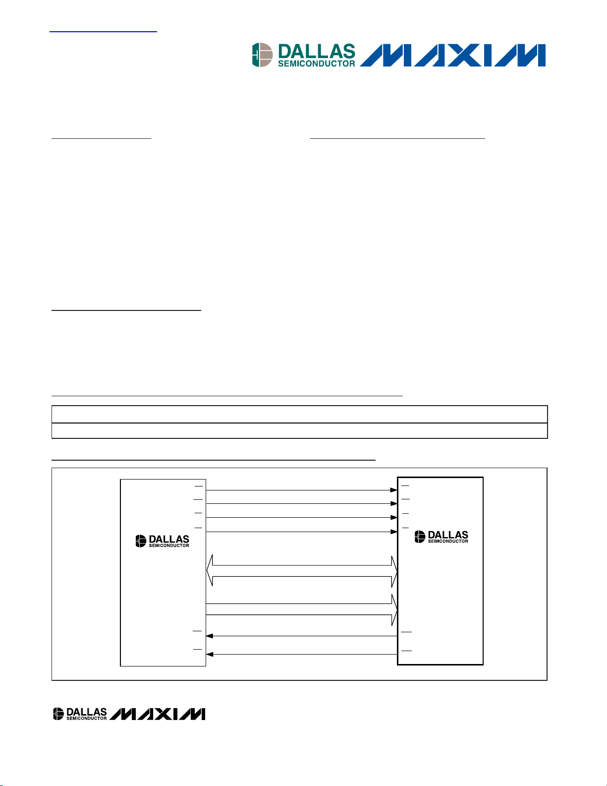
CE
DATA
ADDRESS
INT
RST
A0–18
DQ0–7
CE
19 BITS
8 BITS
MICROPROCESSOR
OR DSP
DS3050W
512k x 8
NV SRAM
AND RTC
WR WE
RD OE
INT
IRQ/FT
CS CS
Typical Operating Circuit
Rev 0; 4/05
For pricing, delivery, and ordering information, please contact Maxim/Dallas Direct! at
1-888-629-4642, or visit Maxim’s website at www.maxim-ic.com.
Ordering Information
Pin Configuration appears at end of data sheet.
PART TEMP RANGE PIN-PACKAGE SPEED
SUPPLY VOLTAGE (%)
DS3050W-100 -40°C to +85°C 256-ball 27mm x 27mm BGA Module 100ns 3.3V ±0.3V
查询DS3050W供应商
Page 2
DS3050W
3.3V Single-Piece 4Mb Nonvolatile SRAM
with Clock
2 _____________________________________________________________________
ABSOLUTE MAXIMUM RATINGS
RECOMMENDED OPERATING CONDITIONS
(TA= -40°C to +85°C.)
Stresses beyond those listed under “Absolute Maximum Ratings” may cause permanent damage to the device. These are stress ratings only, and functional
operation of the device at these or any other conditions beyond those indicated in the operational sections of the specifications is not implied. Exposure to
absolute maximum rating conditions for extended periods may affect device reliability.
Voltage Range on Any Pin Relative to Ground......-0.3V to +4.6V
Operating Temperature Range ...........................-40°C to +85°C
Storage Temperature Range ...............................-40°C to +85°C
Soldering Temperature Range .......See IPC/JEDEC J-STD-020C
PARAMETER
CONDITIONS
UNITS
Supply Voltage V
CC
3.0 3.3 3.6 V
Input Logic 1 V
IH
2.2
V
Input Logic 0 V
IL
0.0 0.4 V
PIN CAPACITANCE
(TA= +25°C.)
PARAMETER
CONDITIONS
UNITS
Input Capacitance C
IN
Not production tested 15 pF
Input/Output Capacitance C
OUT
Not production tested 15 pF
DC ELECTRICAL CHARACTERISTICS
(V
CC
= 3.3V ±0.3V, TA = -40°C to +85°C.)
PARAMETER
CONDITIONS
UNITS
Input Leakage Current I
IL
µA
I/O Leakage Current I
IO
CE = CS = V
CC
µA
Output-Current High I
OH
At 2.4V
mA
Output-Current Low I
OL
At 0.4V 2.0 mA
Output-Current Low RST
At 0.4V (Note 1) 8.0 mA
Output-Current Low IRQ/FT
At 0.4V (Note 1) 7.0 mA
I
CCS1
CE = CS = 2.2V 0.5 7
Standby Current
I
CCS2
CE = CS = V
CC
- 0.2V 0.2 5
mA
Operating Current I
CCO1tRC
= 200ns, outputs open 50 mA
Write Protection Voltage V
TP
2.8
2.9
3.0 V
SYMBOL
SYMBOL
MIN TYP MAX
V
CC
MIN TYP MAX
-1.0 +1.0
-1.0 +1.0
-1.0
IOL RST
IOL IRQ/FT
SYMBOL
MIN TYP MAX
Page 3
DS3050W
3.3V Single-Piece 4Mb Nonvolatile SRAM
with Clock
_____________________________________________________________________ 3
AC ELECTRICAL CHARACTERISTICS
(V
CC
= 3.3V ±0.3V, TA = -40°C to +85°C.)
DS3050W-100
PARAMETER
CONDITIONS
MIN MAX
UNITS
Read Cycle Time
t
RC
100 ns
Access Time
t
ACC
100 ns
OE to Output Valid
t
OE
50 ns
RTC OE to Output Valid
t
OEC
60 ns
CE or CS to Output Valid
t
CO
100 ns
OE or CE or CS to Output Active
t
COE
(Note 2) 5 ns
Output High Impedance from
Deselection
t
OD
(Note 2) 40 ns
Output Hold from Address t
OH
5ns
Write Cycle Time
t
WC
100 ns
Write Pulse Width
t
WP
(Note 3) 75 ns
Address Setup Time
t
AW
0ns
t
WR1
(Note 4) 5
Write Recovery Time
t
WR2
(Note 5) 20
ns
Output High Impedance from WE
t
ODW
(Note 2) 40 ns
Output Active from WE
t
OEW
(Note 2) 5 ns
Data Setup Time
t
DS
(Note 6) 40 ns
t
DH1
(Note 4) 0
Data Hold Time
t
DH2
(Note 5) 20
ns
Chip-to-Chip Setup Time
t
CCS
40 ns
POWER-DOWN/POWER-UP TIMING
(TA = -40°C to +85°C.)
PARAMETER
CONDITIONS
UNITS
VCC Fail Detect to CE, CS, and
WE Inactive
t
PD
(Note 7) 1.5 µs
VCC Slew from VTP to 0V
t
F
µs
VCC Slew from 0V to V
TP
t
R
µs
VCC Valid to CE, CS, and WE
Inactive
t
PU
2ms
VCC Valid to End of Write
Protection
t
REC
ms
VCC Fail Detect to RST Active
t
RPD
(Note 1) 3.0 µs
VCC Valid to RST Inactive
t
RPU
(Note 1) 40 350
ms
SYMBOL
SYMBOL
MIN TYP MAX
150
150
125
525
Page 4
DS3050W
3.3V Single-Piece 4Mb Nonvolatile SRAM
with Clock
4 _____________________________________________________________________
Note 1: IRQ/FT and RST are open-drain outputs and cannot source current. External pullup resistors should be connected to these
pins to realize a logic-high level.
Note 2: These parameters are sampled with a 5pF load and are not 100% tested.
Note 3: t
WP
is specified as the logical AND of CE with WE for SRAM writes, or CS with WE for RTC writes. tWPis measured from
the latter of the two related edges going low to the earlier of the two related edges going high.
Note 4: t
WR1
and t
DH1
are measured from WE going high.
Note 5: t
WR2
and t
DH2
are measured from CE going high for SRAM writes or CS going high for RTC writes.
Note 6: t
DS
is measured from the earlier of CE or WE going high for SRAM writes, or from the earlier of CS or WE going high for
RTC writes.
Note 7: In a power-down condition, the voltage on any pin may not exceed the voltage on V
CC
.
Note 8: The expected t
DR
is defined as accumulative time in the absence of VCCstarting from the time power is first applied by the
user. Minimum expected data-retention time is based upon a maximum of two +230°C convection reflow exposures, followed by a fully charged cell. Full charge occurs with the initial application of V
CC
for a minimum of 96 hours. This parame-
ter is assured by component selection, process control, and design. It is not measured directly during production testing.
Note 9: WE is high for any read cycle.
Note 10: OE = V
IH
or VIL. If OE = VIHduring write cycle, the output buffers remain in a high-impedance state.
Note 11: If the CE or CS low transition occurs simultaneously with or latter than the WE low transition, the output buffers remain in a
high-impedance state during this period.
Note 12: If the CE or CS high transition occurs prior to or simultaneously with the WE high transition, the output buffers remain in a
high-impedance state during this period.
Note 13: If WE is low or the WE low transition occurs prior to or simultaneously with the related CE or CS low transition, the output
buffers remain in a high-impedance state during this period.
DATA RETENTION
(TA= +25°C.)
PARAMETER
CONDITIONS
UNITS
Expected Data-Retention Time
(Per Charge)
t
DR
(Notes 7, 8) 2 3
Years
SYMBOL
MIN TYP MAX
Page 5
DS3050W
3.3V Single-Piece 4Mb Nonvolatile SRAM
with Clock
_____________________________________________________________________ 5
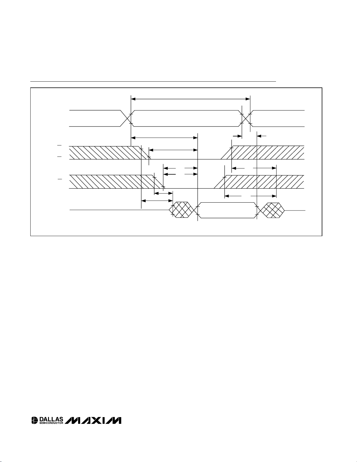
Read Cycle
OUTPUT
DATA VALID
t
RC
t
ACC
t
CO
t
OE
t
OEC
t
OH
t
OD
t
OD
t
COE
t
COE
V
IH
V
IH
V
IL
V
OH
V
OL
V
OH
V
OL
V
IL
V
IH
ADDRESSES
CE
OR
CS
OE
D
OUT
(SEE NOTE 9.)
V
IH
V
IH
V
IH
V
IH
V
IL
V
IL
V
IL
Page 6
DS3050W
3.3V Single-Piece 4Mb Nonvolatile SRAM
with Clock
6 _____________________________________________________________________
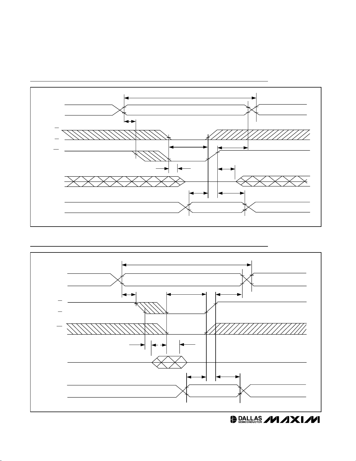
Write Cycle 1
DATA IN STABLE
ADDRESSES
WE
D
OUT
D
IN
t
WC
V
IH
V
IH
V
IH
V
IH
V
IL
V
IL
V
IL
HIGH
IMPEDANCE
V
IH
V
IH
V
IL
V
IL
V
IH
V
IL
V
IL
V
IL
V
IL
t
AW
t
WP
t
OEW
t
DH1
t
DS
t
ODW
t
WR1
(SEE NOTES 2, 3, 4, 6, 10–13.)
CE
OR
CS
Write Cycle 2
t
WC
t
AW
t
DH2
t
DS
t
COE
t
ODW
t
WP
t
WR2
V
IH
V
IL
V
IH
ADDRESSES
WE
D
OUT
D
IN
V
IL
V
IH
V
IL
V
IH
V
IL
V
IL
V
IL
V
IL
V
IH
V
IH
V
IL
V
IH
DATA IN STABLE
V
IL
V
IH
V
IL
(SEE NOTES 2, 3, 5, 6, 10–13.)
CE
OR
CS
Page 7

DS3050W
3.3V Single-Piece 4Mb Nonvolatile SRAM
with Clock
_____________________________________________________________________ 7
Power-Down/Power-Up Condition
t
DR
t
PU
t
F
t
PD
t
RPU
t
RPD
SLEWS WITH
V
CC
t
R
V
OL
V
IH
V
OL
t
REC
V
CC
V
TP
~2.5V
CE,
WE
RST
BACKUP CURRENT
SUPPLIED FROM
LITHIUM BATTERY
(SEE NOTES 1, 7.)
AND
CS
Typical Operating Characteristics
(VCC= 3.3V, TA= +25°C, unless otherwise noted.)
SUPPLY CURRENT
vs. OPERATING FREQUENCY
DS3050W toc01
VCC (V)
SUPPLY CURRENT (mA)
3.53.43.33.23.1
1
2
3
4
5
6
7
0
3.0 3.6
TA = +25°C
5MHz CE-ACTIVATED
50% DUTY CYCLE
1MHz ADDRESS-ACTIVATED
100% DUTY CYCLE
1MHz CE-ACTIVATED
50% DUTY CYCLE
5MHz ADDRESS-ACTIVATED
100% DUTY CYCLE
SUPPLY CURRENT
vs. SUPPLY VOLTAGE
DS3050W toc02
VCC (V)
SUPPLY CURRENT (µA)
3.53.43.33.23.1
600
700
800
900
1000
500
3.0 3.6
VCC = CE = 3.3V,
V
BAT
= V
CHARGE
,
OSC = ON
BATTERY CHARGER CURRENT
vs. BATTERY VOLTAGE
DS3050W toc03
DELTA V BELOW V
CHARGE
(V)
BATTERY CHARGER CURRENT, I
CHARGE
(mA)
0.80.2 0.60.4
1
2
3
4
5
6
7
8
0
01.0
VCC = CE = 3.3V
V
CHARGE
= 2.86V
Page 8

DS3050W
3.3V Single-Piece 4Mb Nonvolatile SRAM
with Clock
8 _____________________________________________________________________
V
CHARGE
PERCENT CHANGE
vs. TEMPERATURE
DS3050W toc04
TEMPERATURE (°C)
VC
HARGE
PERCENT CHANGE FROM 25°C (%)
603510-15
-0.5
0
0.5
1.0
-1.0
-40 85
VCC = 3.3V,
V
BAT
= V
CHARGE
WRITE PROTECTION VOLTAGE
vs. TEMPERATURE
DS3050W toc05
TEMPERATURE (°C)
WRITE PROTECT, V
TP
(V)
603510-15
2.85
2.90
2.95
3.00
2.80
-40 85
DQ OUTPUT-VOLTAGE HIGH
vs. DQ OUTPUT-CURRENT HIGH
DS3050W toc06
IOH (mA)
V
OH
(V)
-1-2-3-4
2.7
2.9
3.1
3.3
3.5
2.5
-5 0
VCC = 3.3V
DQ OUTPUT-VOLTAGE LOW
vs. DQ OUTPUT-CURRENT LOW
DS3050W toc07
IOL (mA)
V
OL
(V)
4321
0.1
0.2
0.3
0.4
0
05
VCC = 3.3V
IRQ/FT OUTPUT-VOLTAGE LOW
vs. OUTPUT-CURRENT LOW
DS3050W toc08
IOL (mA)
V
OL
(V)
15105
0.1
0.2
0.3
0.4
0.5
0.6
0
020
RST OUTPUT-VOLTAGE LOW
vs. OUTPUT-CURRENT LOW
DS3050W toc09
IOL (mA)
V
OL
(V)
15105
0.1
0.2
0.3
0.4
0.5
0.6
0
020
Typical Operating Characteristics (continued)
(VCC= 3.3V, TA= +25°C, unless otherwise noted.)
RST VOLTAGE
vs. V
CC
DURING POWER-UP
DS3050W toc10
VCC POWER-UP (V)
RST VOLTAGE W/PULLUP RESISTOR (V)
3.53.00.5 1.0 1.5 2.0 2.5
0.5
1.0
1.5
2.0
2.5
3.0
3.5
4.0
0
0 4.0
TA = +25°C
Page 9

DS3050W
3.3V Single-Piece 4Mb Nonvolatile SRAM
with Clock
_____________________________________________________________________ 9
Pin Description
BALLS
DESCRIPTION
A1, A2, A3, A4
Ground
B1, B2, B3, B4
Interrupt/Frequency Test
Output
C1, C2, C3, C4
Address Input 15
D1, D2, D3, D4
Address Input 16
E1, E2, E3, E4
Reset Output
F1, F2, F3, F4
Supply Voltage
G1, G2, G3, G4
Write Enable Input
H1, H2, H3, H4 OE Output Enable Input
J1, J2, J3, J4 CE SRAM Chip Enable Input
K1, K2, K3, K4
Data Input/Output 7
L1, L2, L3, L4
Data Input/Output 6
M1, M2, M3, M4
Data Input/Output 5
N1, N2, N3, N4
Data Input/Output 4
P1, P2, P3, P4
Data Input/Output 3
R1, R2, R3, R4
Data Input/Output 2
T1, T2, T3, T4
Data Input/Output 1
U1, U2, U3, U4
Data Input/Output 0
V1, V2, V3, V4
Ground
W1, W2, W3, W4
Ground
Y1, Y2, Y3, Y4
Ground
A17, A18, A19, A20
Ground
B17, B18, B19, B20
Address Input 18
C17,C18,C19, C20
Address Input 17
D17, D18, D19, D20
Address Input 14
E17, E18, E19, E20
Address Input 13
F17, F18, F19, F20
Address Input 12
G17, G18, G19, G20
Address Input 11
H17, H18, H19, H20
Address Input 10
J17, J18, J19, J20 A9 Address Input 9
K17, K18, K19, K20 A8 Address Input 8
L17, L18, L19, L20 A7 Address Input 7
M17, M18, M19, M20 A6 Address Input 6
NAME
GND
IRQ/FT
A15
A16
RST
V
CC
WE
DQ7
DQ6
DQ5
DQ4
DQ3
DQ2
DQ1
DQ0
GND
GND
GND
GND
A18
A17
A14
A13
A12
A11
A10
BALLS NAME DESCRIPTION
N17, N18, N19, N20 A5 Address Input 5
P17, P18, P19, P20 A4 Address Input 4
R17, R18, R19, R20 A3 Address Input 3
T17, T18, T19, T20 A2 Address Input 2
U17, U18, U19, U20 A1 Address Input 1
V17, V18, V19, V20 A0 Address Input 0
W17, W18, W19, W20 GND Ground
Y17, Y18, Y19, Y20 GND Ground
A5, B5, C5, D5 N.C. No Connection
A6, B6, C6, D6 N.C. No Connection
A7, B7, C7, D7 N.C. No Connection
A8, B8, C8, D8 N.C. No Connection
A9, B9, C9, D9 N.C. No Connection
A10, B10, C10, D10 V
A11, B11, C11, D11 N.C. No Connection
A12, B12, C12, D12 N.C. No Connection
A13, B13, C13, D13 N.C. No Connection
A14, B14, C14, D14 N.C. No Connection
A15, B15, C15, D15 N.C. No Connection
A16, B16, C16, D16 N.C. No Connection
U5, V5, W5, Y5 CS RTC Chip Select
U6, V6, W6, Y6 N.C. No Connection
U7, V7, W7, Y7 N.C. No Connection
U8, V8, W8, Y8 N.C. No Connection
U9, V9, W9, Y9 N.C. No Connection
U10, V10, W10, Y10 N.C. No Connection
U11, V11, W11, Y11 N.C. No Connection
U12, V12, W12, Y12 N.C. No Connection
U13, V13, W13, Y13 N.C. No Connection
U14, V14, W14, Y14 N.C. No Connection
U15, V15, W15, Y15 N.C. No Connection
U16, V16, W16, Y16 N.C. No Connection
Supply Voltage
CC
Page 10

DS3050W
3.3V Single-Piece 4Mb Nonvolatile SRAM
with Clock
10 ____________________________________________________________________
Functional Diagram
CURRENT-LIMITING
RESISTOR
BATTERY-CHARGING/SHORTING
PROTECTION CIRCUITRY (U.L. RECOGNIZED)
REDUNDANT LOGIC
DELAY TIMING
CIRCUITRY
CHARGER
CURRENT-LIMITING
RESISTOR
V
TP
REF
V
SW
REF
GND
ML
CE
RST
CE
REDUNDANT
SERIES FET
SRAM
DQ0–7
OE
WE
V
CC
V
CC
UNINTERRUPTED
POWER SUPPLY
FOR THE SRAM
AND RTC
IRQ/FT
DS3050W
OE
WE
A0–A18
A0-A3
REAL-TIME
CLOCK
32.768kHz
WE
OE
CS
CS
Page 11

DS3050W
3.3V Single-Piece 4Mb Nonvolatile SRAM
with Clock
____________________________________________________________________ 11
Detailed Description
The DS3050W is a 4Mb (512k x 8 bits) fully static, NV
memory similar in function and organization to the
DS1250W NV SRAM, but also containing an RTC and
rechargeable ML battery. The DS3050W NV SRAM constantly monitors VCCfor an out-of-tolerance condition.
When such a condition occurs, the lithium energy source
is automatically switched on and write protection is
unconditionally enabled to prevent data corruption. There
is no limit to the number of write cycles that can be executed, and no additional support circuitry is required for
microprocessor interfacing. This device can be used in
place of SRAM, EEPROM, or flash components.
User access to either the SRAM or the real-time clock
registers is accomplished with a byte-wide interface
and discrete control inputs, allowing for a direct interface to many 3.3V microprocessor devices.
The DS3050W RTC contains a full-function, year 2000compliant (Y2KC) clock/calendar with an RTC alarm,
watchdog timer, battery monitor, and power monitor.
RTC registers contain century, year, month, date, day,
hours, minutes, and seconds data in a 24-hour BCD
format. Corrections for day of the month and leap year
are made automatically.
The DS3050W RTC registers are double-buffered into
an internal and external set. The user has direct access
to the external set. Clock/calendar updates to the external set of registers can be disabled and enabled to
allow the user to access static data. Assuming the
internal oscillator is on, the internal registers are contin-
ually updated, regardless of the state of the external
registers, assuring that accurate RTC information is
always maintained.
The DS3050W contains interrupt (IRQ/FT) and reset
(RST) outputs, which can be used to control CPU activ-
ity. The IRQ/FT interrupt output can be used to generate an external interrupt when the RTC register values
match user-programmed alarm values. The interrupt is
always available while the device is powered from the
system supply, and it can be programmed to occur
when in the battery-backed state to serve as a system
wake-up. The IRQ/FT output can also be used as a
CPU watchdog timer. CPU activity is monitored and an
interrupt can be activated if the correct activity is not
detected. The RST output can be used to detect a system power-down or failure and hold the CPU in a safe
state until normal power returns.
The DS3050W constantly monitors the voltage of the
internal battery. The battery-low flag (BLF) in the RTC
FLAGS register is not writeable and should always be a
0 when read. Should a 1 ever be present, the battery
voltage is below ∼2V and the contents of the clock and
SRAM are questionable.
The DS3050W module is constructed on a standard 256ball, 27mm x 27mm BGA substrate. Unlike other surface-mount NV memory modules that require the battery
to be removable for soldering, the internal ML battery
can tolerate exposure to convection reflow soldering
temperatures, allowing this single-piece component to
be handled with standard BGA assembly techniques.
Table 1. RTC/Memory Operational Truth Table
CS WE CE OE MODE ICC OUTPUTS
01 10 RTC Read Active Active
01 11 RTC Read Active High Impedance
00 1X RTC Write Active High Impedance
11 00SRAM Read Active Active
11 01SRAM Read Active High Impedance
10 0X SRAM Write Active High Impedance
1X 1X Standby Standby High Impedance
0X 0X Invalid
(1)
Active Invalid
X = Don’t care.
(1)
= See Figure 4.
Page 12

DS3050W
3.3V Single-Piece 4Mb Nonvolatile SRAM
with Clock
12 ____________________________________________________________________
SRAM Read Mode
The DS3050W executes an SRAM read cycle whenever
CS (RTC chip select) and WE (write enable) are inactive
(high) and CE (SRAM chip enable) is active (low). The
unique address specified by the 19 address inputs (A0
to A18) defines which of the 524,288 bytes of SRAM data
is to be accessed. Valid data will be available to the
eight data output drivers within t
ACC
(access time) after
the last address input signal is stable, providing that CE
and OE (output enable) access times are also satisfied.
If CE and OE access times are not satisfied, then data
access must be measured from the later occurring signal (CE or OE) and the limiting parameter is either tCOfor
CE or tOEfor OE rather than address access.
SRAM Write Mode
The DS3050W executes an SRAM write cycle whenever
CS is inactive (high) and the CE and WE signals are
active (low) after address inputs are stable. The lateroccurring falling edge of CE or WE determines the start of
the write cycle. The write cycle is terminated by the earlier
rising edge of CE or WE. All address inputs must be kept
valid throughout the write cycle. WE must return to the
high state for a minimum recovery time (tWR) before
another cycle can be initiated. The CS and OE control
signal should be kept inactive (high) during SRAM write
cycles to avoid bus contention. However, if the output drivers have been enabled (CE and OE active) then WE dis-
ables the outputs in t
ODW
from its falling edge.
DATA
B7 B6 B5 B4 B3 B2 B1 B0
FUNCTION/RANGE
xxxxFh 10 YEAR YEAR YEAR 00–99
xxxxEh X X X 10 M MONTH MONTH 01–12
xxxxDh X X 10 DATE DATE DATE 01–31
xxxxCh X FT X X X DAY DAY 01–07
xxxxBh X X 10 HOUR HOUR HOUR 00–23
xxxxAh X 10 MINUTES MINUTES MINUTES 00–59
xxxx9h OSC 10 SECONDS SECONDS SECONDS 00–59
xxxx8h W R 10 CENTURY CENTURY CONTROL 00–39
xxxx7h WDS
RB1 RB0
xxxx6h AE Y ABE Y Y Y Y Y
xxxx5h AM4 Y 10 DATE DATE
01–31
xxxx4h AM3 Y 10 HOURS HOURS
ALARM
HOURS
00–23
xxxx3h AM2 10 MINUTES MINUTES
ALARM
MINUTES
00–59
xxxx2h AM1 10 SECONDS SECONDS
ALARM
SECONDS
00–59
xxxx1h Y Y Y Y Y Y Y Y UNUSED
xxxx0h WF AF 0 BLF 0 0 0 0 FLAGS
x = Don’t care address bits.
X = Unused. Read/writeable under write and read bit control.
FT = Frequency test bit.
OSC = Oscillator start/stop bit.
W = Write bit.
R = Read bit.
WDS = Watchdog steering bit.
BMB0–BMB4 = Watchdog multiplier bits.
RB0, RB1 = Watchdog resolution bits.
AE = Alarm flag enable.
Y = Unused. Read/writeable without write and read bit control.
ABE = Alarm in backup mode enable.
AM1–AM4 = Alarm mask bits.
WF = Watchdog flag.
AF = Alarm flag.
0 = Reads as a 0 and cannot be changed.
BLF = Battery low flag.
Clock Operations
Table 2. RTC Register Map
ADDRESS
BMB4 BMB3 BMB2 BMB1 BMB0
WATCHDOG
INTERRUPTS
ALARM DATE
Page 13

DS3050W
3.3V Single-Piece 4Mb Nonvolatile SRAM
with Clock
____________________________________________________________________ 13
RTC Read Mode
The DS3050W executes an RTC read cycle whenever
CE (SRAM chip enable) and WE (write enable) are
inactive (high) and CS (RTC chip select) is active (low).
The least significant 4 address inputs (A0 to A3) define
which of the 16 RTC registers is to be accessed (see
Table 2). Valid data is available to the eight data output
drivers within t
ACC
(access time) after the last address
input signal is stable, providing that CS and OE (output
enable) access times are also satisfied. If CS and OE
access times are not satisfied, then data access must
be measured from the later occurring signal (CS or OE)
and the limiting parameter is either tCOfor CS or t
OEC
for OE rather than address access.
RTC Write Mode
The DS3050W executes an RTC write cycle whenever
CE is inactive (high) and the CS and WE signals are
active (low) after address inputs are stable. The lateroccurring falling edge of CS or WE determines the start
of the write cycle. The write cycle is terminated by the
earlier rising edge of CS or WE. All address inputs must
be kept valid throughout the write cycle. WE must return
to the high state for a minimum recovery time (tWR)
before another cycle can be initiated. The CE and OE
control signals should be kept inactive (high) during RTC
write cycles to avoid bus contention. However, if the output drivers have been enabled (CS and OE active) then
WE disables the outputs in t
ODW
from its falling edge.
Clock Oscillator Mode
The oscillator can be turned off to minimize battery current drain. The OSC bit is the MSB of the SECONDS
register, and must be initialized to a 0 to start the oscillator upon first power application. The OSC bit is factory set to a 1 prior to shipment. Oscillator operation and
frequency can be verified by setting the FT bit to a 1
and monitoring the IRQ/FT output for 512Hz.
Reading the Clock
When reading the RTC data, it is recommended to halt
updates to the external set of double-buffered RTC registers. This puts the external registers into a static state,
allowing the data to be read without register values
changing during the read process. Normal updates to
the internal registers continue while in this state.
External updates are halted by writing a 1 to the read
bit (R). As long as a 1 remains in the R bit, updating is
inhibited. After a halt is issued, the registers reflect the
RTC count (day, date, and time) that was current at the
moment the halt command was issued. Normal
updates to the external set of registers resume within 1
second after the R bit is set to a 0 for a minimum of
500µs. The R bit must be a 0 for a minimum of 500µs to
ensure the external registers have fully updated.
Setting the Clock
As with a clock read, it is also recommended to halt
updates prior to setting new time values. Setting the
write bit (W) to a 1 halts updates of the external RTC
registers 8h to Fh. After setting the W bit to a 1, the RTC
registers can be loaded with the desired count (day,
date, and time) in BCD format. Setting the W bit to a 0
then transfers the values written to the internal registers
and allows normal clock operation to resume.
Frequency Test Mode
The DS3050W frequency test mode uses the IRQ/FT
open-drain output. With the oscillator running, the
IRQ/FT output toggles at 512Hz when the FT bit is a 1,
the alarm-flag enable bit (AE) is a 0, and the watchdogenable bit (WDS) is a 1 or the WATCHDOG register is
written to 00h (FT • AE • (WDS + WATCHDOG)). The
IRQ/FT output and the frequency test mode can be
used to measure the actual frequency of the 32.768kHz
RTC oscillator. The FT bit is reset to a 0 on power-up.
Using the Clock Alarm
The alarm settings and control for the DS3050W reside
within RTC registers 2h–5h. The INTERRUPTS register
(6h) contains two alarm-enable bits: alarm enable (AE)
and alarm in backup enable (ABE). The AE and ABE
bits must be set as described below for the IRQ/FT output to be activated when an alarm match occurs.
The alarm can be programmed to activate on a specific
day of the month or repeat every day, hour, minute, or
second. It can also be programmed to go off while the
DS3050W is in the Data Retention Mode to serve as a
system wake-up. Alarm mask bits AM1 to AM4 control
the alarm mode (see Table 3). Configurations not listed
in the table will default to the once-per-second mode to
notify the user of an incorrect alarm setting.
Page 14

DS3050W
3.3V Single-Piece 4Mb Nonvolatile SRAM
with Clock
14 ____________________________________________________________________
When the RTC register values match alarm register settings, the alarm flag (AF) is set to a 1. If AE is also a 1,
the alarm condition activates the IRQ/FT output. When
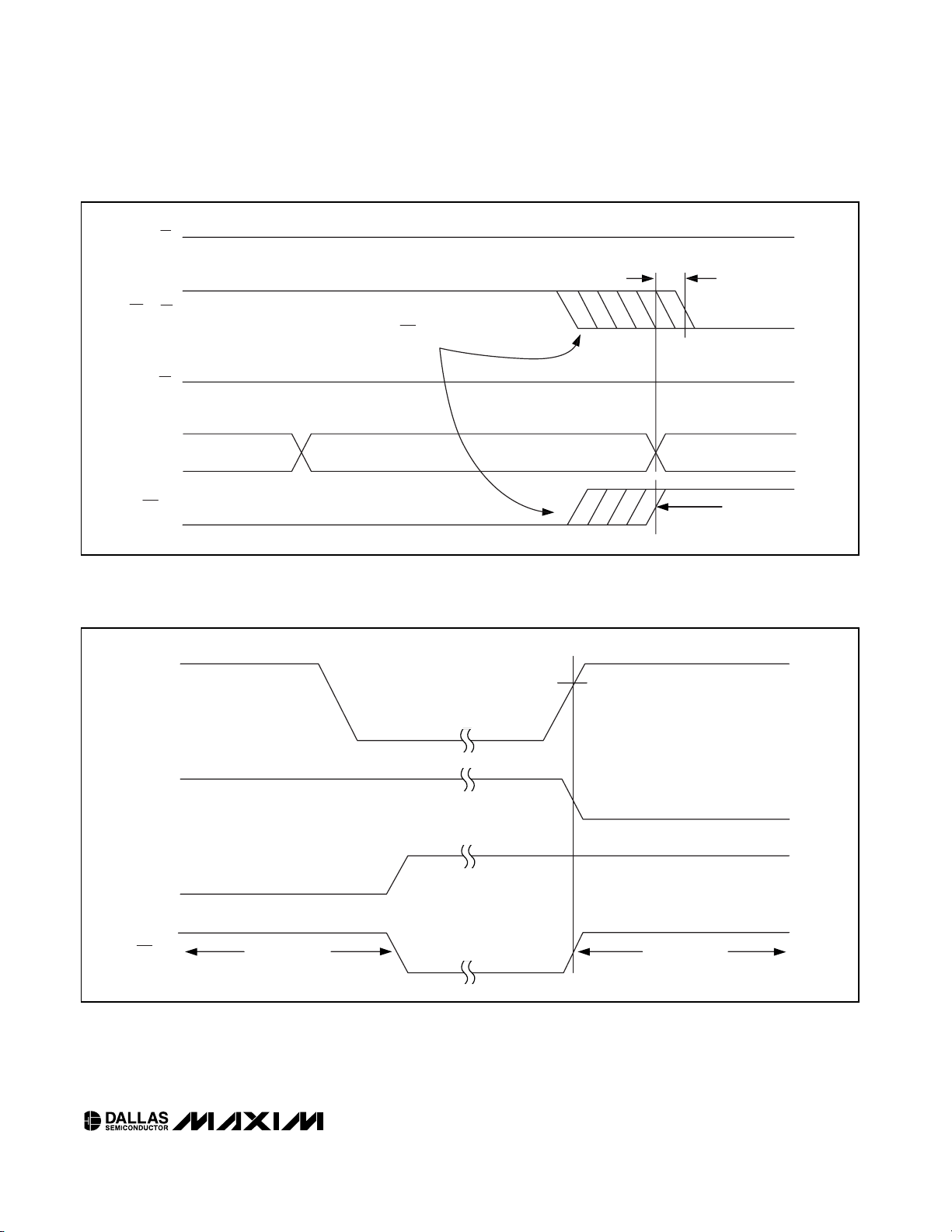
CS is active, the IRQ/FT signal can be cleared by holding the FLAGS register address stable for tRCand forcing either OE or WE active (see Figure 1). The flag does
not change state until the end of the read/write cycle
and after the IRQ/FT signal has deasserted. To avoid
inadvertently clearing the IRQ/FT signal while preparing
for subsequent write/read cycles at other register
addresses, assure that tAWis met for that subsequent
address (see Figure 2).
The IRQ/FT output can also be activated during battery
backup mode. The IRQ/FT goes low if an alarm occurs
and both AE and ABE are set to 1. The AE and ABE
bits are reset to 0 during the power-up transition, but an
alarm generated during power-up will set AF to a 1.
Therefore, the AF bit can be read after system powerup to determine if an alarm was generated during the
power-up sequence. Figure 3 illustrates alarm timing
during battery backup mode and power-up states.
Table 3. Alarm Mask Bits
AM4 AM3 AM2 AM1 ALARM RATE
1111Once per second
1110When seconds match
1100When minutes and seconds match
1000When hours, minutes, and seconds match
0000When date, hours, minutes, and seconds match
Figure 1. Clearing Active IRQ Waveforms
CE
WE OR OE
CS
t
MAX
RC
A0–A3
IRQ/FT
ADDRESS 0h
HIGH IMPEDANCE
Page 15
DS3050W
3.3V Single-Piece 4Mb Nonvolatile SRAM
with Clock
____________________________________________________________________ 15
CE
WE OR OE
CS
A0–A3
IRQ/FT
t
AS
ADDRESS 0h
ADDRESS Xh
INTENTIONAL WRITE OR
READ AT ADDRESS Xh
INADVERTENT WRITE OR READ OF
RTC FLAGS REGISTER
WILL RESET IRQ/FT
HIGH IMPEDANCE
Figure 2. Prevent Accidental Clearing of IRQ Waveforms
V
CC
V
TP
ABE, AE
AF
IRQ/FT
HIGH IMPEDANCE
HIGH IMPEDANCE
Figure 3. Battery Backup Mode Alarm Waveforms
Page 16

DS3050W
3.3V Single-Piece 4Mb Nonvolatile SRAM
with Clock
16 ____________________________________________________________________
Using the Watchdog Timer
The watchdog timer can be used to detect an out-ofcontrol processor. The user programs the watchdog
timer by setting the desired timeout delay into the
WATCHDOG register. The five high-order WATCHDOG
register bits store a binary multiplier and the two lowerorder WATCHDOG bits select the resolution, where 00
= 1/16second, 01 = 1/4second, 10 = 1 second, and 11
= 4 seconds. The watchdog timeout value is then
determined by multiplication of the 5-bit multiplier value
with the 2-bit resolution value. (For example: writing
00001110 (0Eh) into the WATCHDOG register = 3 x 1
second, or 3 seconds.) If the processor does not reset
the timer within the specified period, the watchdog flag
(WF) is set to a 1 and a processor interrupt is generated and stays active until either WF is read or the
WATCHDOG register is read or written.
The MSB of the WATCHDOG register is the watchdog
steering bit (WDS). When WDS is set to a 0, the watchdog activates the IRQ/FT output when the watchdog
times out. WDS should not be written to a 1, and should
be initialized to a 0 if the watchdog function is enabled.
The watchdog timer resets when the processor performs a read or write of the WATCHDOG register. The
timeout period then starts over. The watchdog timer is
disabled by writing a value of 00h to the WATCHDOG
register. The watchdog function is automatically disabled upon power-up and the WATCHDOG register is
cleared to 00h.
Power-On Default States
Upon each application of power to the device, the following register bits are automatically set to 0:
WDS = 0, BMB0–BMB4 = 0, RB0, RB1 = 0, AE = 0,
ABE = 0.
All other RTC bits are undefined.
Data-Retention Mode
The DS3050W provides full functional capability for V
CC
greater than 3.0V and write-protects by 2.8V. Data is
maintained in the absence of VCCwithout additional
support circuitry. The NV SRAM constantly monitors
VCC. Should the supply voltage decay, the NV SRAM
automatically write-protects itself. All inputs become
don’t care, and all data outputs become high impedance. As VCCfalls below approximately 2.5V (VSW), the
power-switching circuit connects the lithium energy
source to the clock and SRAM to maintain time and
retain data. During power-up, when VCCrises above
VSW, the power-switching circuit connects external V
CC
to the clock and SRAM, and disconnects the lithium
energy source. Normal clock or SRAM operation can
resume after VCCexceeds VTPfor a minimum duration
of t
REC
.
Battery Charging
When VCCis greater than VTPan internal regulator will
charge the battery. The UL-approved charger circuit
includes short-circuit protection and a temperature-stabilized voltage reference for on-demand charging of
the internal battery. Typical data retention expectations
greater than 2 years per charge cycle are achievable.
A maximum of 96 hours of charging time is required to
fully charge a depleted battery.
System Power Monitoring
When the external VCCsupply falls below the selected
out-of-tolerance trip point, the output RST is forced
active (low). Once active, the RST is held active until
the VCCsupply has fallen below that of the internal battery. On power-up, the RST output is held active until
the external supply is greater than the selected trip
point and one reset timeout period (t
RPU
) has elapsed.
This is sufficiently longer than t
REC
to ensure that the
RTC and SRAM are ready for access by the microprocessor.
Freshness Seal and Shipping
The DS3050W is shipped from Dallas Semiconductor
with the RTC oscillator disabled and the lithium battery
electrically disconnected, guaranteeing that no battery
capacity has been consumed during transit or storage.
As shipped, the lithium battery is ~60% charged, and
no pre-assembly charging operations should be
attempted.
When VCCis first applied at a level greater than VTP,
the lithium battery is enabled for backup operation. The
user is required to enable the oscillator (MSB of SECONDS register) and initialize the required RTC registers
for proper timekeeping operation. A 96 hour initial battery charge time is recommended for new system
installations.
Applications Information
Power-Supply Decoupling
To achieve the best results when using the DS3050W,
assure that all VCCand GND balls are connected and
decouple the power supply with a 0.1µF capacitor. Use
a high-quality, ceramic surface-mount capacitor if possible. Surface-mount components minimize lead inductance, which improves performance, and ceramic
capacitors tend to have adequate high-frequency
response for decoupling applications.
Page 17

DS3050W
3.3V Single-Piece 4Mb Nonvolatile SRAM
with Clock
____________________________________________________________________ 17
Avoiding Data Bus Contention
Care should be taken to avoid simultaneous access of
the SRAM and RTC devices (see Figure 4). Any chipenable overlap violates t
CCS
and can result in invalid
and unpredictable behavior.
Using the Open-Drain
IRQ
/FT
and
RST
Outputs
The IRQ/FT and RST outputs are open drain, and there-
fore require pullup resistors to realize a high logic output level. Pullup resistor values between 1kΩ and 10kΩ
are typical.
Battery Charging/Lifetime
The DS3050W charges an ML battery to maximum
capacity in approximately 96 hours of operation when
VCCis greater than VTP. Once the battery is charged,
its lifetime depends primarily on the VCCduty cycle.
The DS3050W can maintain data from a single, initial
charge for up to 2 years. Once recharged, this deepdischarge cycle can be repeated for up to 20 times,
producing a worst-case service life of 40 years. More
typical duty cycles are of shorter duration, enabling the
DS3050W to be charged hundreds of times, and
extending the service life well beyond 40 years.
Recommended Cleaning
Procedures
The DS3050W can be cleaned using aqueous-based
cleaning solutions. No special precautions are needed
when cleaning boards containing a DS3050W module.
Removal of the topside label violates the environmental
integrity of the package and voids the warranty of the
product.
t
CCS
t
CCS
CE
V
IH
V
IH
V
IH
V
IH
CS
Figure 4. SRAM/RTC Data Bus Control
Recommended Reflow Temperature
Profile
PROFILE FEATURE
Sn-Pb EUTECTIC
ASSEMBLY
Average Ramp-Up Rate
(T
L
to TP)
3°C/Second Max
Preheat
- Temperature Min (T
Smin
)
- Temperature Max (T
Smax
)
- Time (Min to Max) (ts)
100°C
150°C
60 to 120 Seconds
T
Smax
to T
L
- Ramp-Up Rate
Time maintained above:
- Temperature (T
L
)
- Time (t
L
)
+183°C
60 to 150 Seconds
Peak Temperature (TP)
225 +0/-5°C
Time Within 5°C of Actual Peak
Temperature (T
P
)
10 to 30 Seconds
Ramp-Down Rate 6°C/Second Max
6 Minutes Max
Note: All temperatures refer to topside of the package, measured on the package body surface.
Time 25°C to Peak Temperature
Page 18

DS3050W
3.3V Single-Piece 4Mb Nonvolatile SRAM
with Clock
Maxim cannot assume responsibility for use of any circuitry other than circuitry entirely embodied in a Maxim product. No circuit patent licenses are
implied. Maxim reserves the right to change the circuitry and specifications without notice at any time.
18 ____________________Maxim Integrated Products, 120 San Gabriel Drive, Sunnyvale, CA 94086 408-737-7600
© 2005 Maxim Integrated Products Printed USA is a registered trademark of Maxim Integrated Products, Inc.
is a registered trademark of Dallas Semiconductor Corporation.
DS3050W BGA modules are recognized by Underwriters Laboratory (UL) under file E99151.
Pin Configuration
A
12
34
789
0
5
6
7
8
90
1
2
34
56
1
2
34 1
1
1
2
5
678
9
1
1
1
1
1
1
1
11
1
2
1
1
1
11
1
1
7
8
9
0
0
1
2
3
4
5
6
DS3050W
B
C
D
E
F
G
H
J
K
L
M
N
P
R
T
U
V
W
Y
A
B
C
D
E
F
G
H
J
K
L
M
N
P
R
T
U
V
W
Y
TOP VIEW
GND
IRQ/FT
A15
A16
RST
V
CC
WE
OE
CE
DQ7
DQ6
DQ5
DQ4
DQ3
DQ2
DQ1
DQ0
GND
GND
GND
GND
A18
A17
A14
A13
A12
A11
A10
A9
A8
A7
A6
A5
A4
A3
A2
A1
A0
GND
GND
CS
N.C.
N.C.
N.C.
N.C.
N.C.
N.C.
N.C.
N.C.
N.C.
N.C.
N.C.
N.C.
N.C.
N.C.
N.C.
N.C.
V
CC
N.C.
N.C.
N.C.
N.C.
N.C.
N.C.
Package Information
(The package drawing(s) in this data sheet may not reflect the most current specifications. For the latest package outline information
go to www.maxim-ic.com/packages
.)
 Loading...