

Page 1
Y
r
1-Wire Digital Thermomete
DS28EA00
with Sequence Detect and PIO
www.maxim-ic.com
GENERAL DESCRIPTION
The DS28EA00 is a digital thermometer with 9-bit
(0.5°C) to 12-bit (1/16°C) resolution and alarm
function with nonvolatile (NV), user-programmable
upper and lower trigger points. Each DS28EA00 has
its unique 64-bit registration number that is factoryprogrammed into the chip. Data is transferred serially
through the 1-Wire
®
protocol, which requires only one
data line and a ground for communication. The
improved 1-Wire front end with hysteresis and glitch
filter enables the DS28EA00 to perform reliably in
large 1-Wire networks. Unlike other 1-Wire thermometers, the DS28EA00 has two additional pins to
implement a sequence detect function. This feature
allows the user to discover the registration numbers
according to the physical device location in a chain,
e.g., to measure the temperature in a storage tower
at different height. If the sequence detect function is
not needed, these pins can be used as generalpurpose input or output. The DS28EA00 can derive
the power for its operation directly from the data line
(“parasite power”), eliminating the need for an
external power supply.
APPLICATIONS
Data Communication Equipment
Process Temperature Monitoring
HVAC Systems
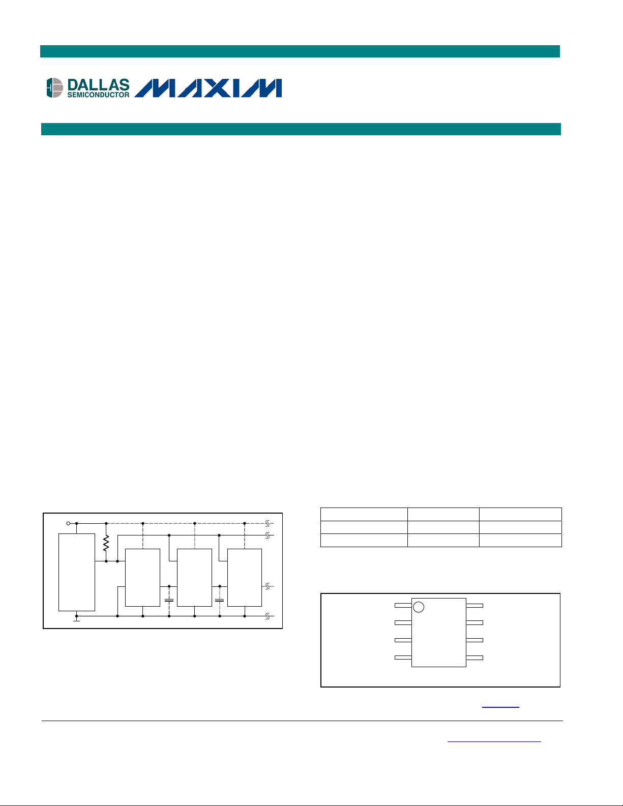
TYPICAL OPERATING CIRCUIT
V
DD
1-Wire
Master
PX.
(Micro-
controller)
Schematic shows PIOs wired for sequence detect function.
Commands, Registers, and Modes are capitalized for
clarity.
1-Wire is a registered trademark of Dallas Semiconductor.
Note: Some revisions of this device may incorporate deviations from published specifications known as errata. Multiple revisions of any device
may be simultaneously available through various sales channels. For information about device errata, click here: www.maxim-ic.com/errata
1 of 29
#1 #2
VDD
IO
DS28EA00
PIOB PIOA
GND
IO
PIOB PIOA
VDD
DS28EA00
GND
#3
VDD
IO
DS28EA00
PIOB PIOA
GND
SPECIAL FEATURES
Digital Thermometer Measures Temperatures
from -40°C to +85°C
Thermometer Resolution is User-Selectable
from 9 to 12 Bits
Unique 1-Wire Interface Requires Only One
Port Pin for Communication
Each Device has a Unique 64-Bit Factory-
Lasered Registration Number
ROM Multidrop Capability Simplifies
Distributed Temperature-Sensing
Applications
Improved 1-Wire Interface with Hysteresis
and Glitch Filter
User-Definable Nonvolatile (NV) Alarm
Threshold Settings/User Bytes
Alarm Search Command to Quickly Identify
Devices Whose Temperature is Outside of
Programmed Limits
Standard and Overdrive 1-Wire Speed
Two General-Purpose Programmable IO (PIO)
Pins
Chain Function Sharing the PIO Pins to
Detect Physical Sequence of Devices in
Network
Operating Range: 3.0V to 5.5V, -40°C to +85°C
Can be Powered from Data Line
8-Pin µSOP Package
ORDERING INFORMATION
PART TEMP RANGE PACKAGE
DS28EA00U+ -40 to +85°C 8-pin µSOP
DS28EA00U+T -40 to +85°C Tape & Reel
+ Denotes lead-free package.
PIN CONFIGURATION
IO
NC
NC
GND
+
8
1
7
2
6
3
5
4
µSOP
Package Outline Drawing 21-0036
V
DD
PIOB
PIOA
NC
.
012907
Page 2

DS28EA00 1-Wire Digital Thermometer with Sequence Detect and PIO
ABSOLUTE MAXIMUM RATINGS
IO Voltage to GND -0.5V, +6V
IO Sink Current 20mA
Maximum PIOA or PIOB Pin Current 20mA
Maximum Current Through GND Pin 40mA
Operating Temperature Range -40°C to +85°C
Junction Temperature +150°C
Storage Temperature Range -40°C to +85°C
Soldering Temperature See IPC/JEDEC J-STD-020
Stresses beyond those listed under “Absolute Maximum Ratings” may cause permanent damage to the device. These are stress ratings only,
and functional operation of the device at these or any other conditions beyond those indicated in the operational sections of the specifications is
not implied. Exposure to the absolute maximum rating conditions for extended periods may affect device.
ELECTRICAL CHARACTERISTICS
(T
= -40°C to +85°C; see Note 1)
A
PARAMETER SYMBOL CONDITIONS MIN TYP MAX UNITS
Power Supply
Supply Voltage V
Supply Current (Note 5) I
Standby Current I
DD
DD
DDS
(Note 2) 3.0 5.5 V
VDD = 5.5V 1.5 mA
VDD = 5.5V 1.5 µA
IO Pin General Data
1-Wire Pullup Voltage
(Note 2)
1-Wire Pullup Resistance R
V
PUP
PUP
Local power 3.0 V
Parasite power 3.0 5.5
(Notes 2, 3)
Input Capacitance CIO (Notes 4, 5) 1000 pF
Input Load Current I
High-to-Low Switching
Threshold
2, 8)
Low-to-High Switching
Threshold (Notes 5, 6, 9)
Switching Hysteresis
(Notes 5, 6, 10)
Output Low Voltage
(Note 11)
Recovery Time
(Notes 2, 12)
(Notes 5, 13)
(Notes 2, 14)
t
L
V
TL
V
IL
V
TH
V
HY
V
OL
t
REC
t
REH
SLOT
IO pin at V
0.1 1.5 µA
PUP
(Notes 5, 6, 7) 0.46
Parasite powered 0.5 Input Low Voltage (Notes
VDD powered (Note 5) 0.7
Parasite power 1.0
Parasite power 0.21 1.7 V
At 4mA 0.4 V
Standard speed, R
Overdrive speed, R
= 2.2kΩ
PUP
PUP
= 2.2kΩ
Overdrive speed, directly prior to reset
pulse; R
= 2.2kΩ
PUP
Standard speed 0.5 5.0 Rising-Edge Hold-Off Time
Overdrive speed Not applicable (0)
Standard speed 65 Timeslot Duration
Overdrive speed 8
IO Pin, 1-Wire Reset, Presence Detect Cycle
Reset Low Time (Note 2) t
Time
(Notes 5, 15)
Time
Time (Notes 2,16)
RSTL
t
PDH
t
FPD
t
PDL
t
MSP
Standard speed 480 640
Overdrive speed 48 80
Standard speed 15 60 Presence-Detect High
Overdrive speed 2 6
Standard speed 1.125 8.1 Presence-Detect Fall Time
Overdrive speed 0 1.3
Standard speed 60 240 Presence-Detect Low
Overdrive speed 8 24
Standard speed 68.1 75 Presence-Detect Sample
Overdrive speed 7.3 10
DD
0.3 2.2
-
V
PUP
1.9V
V
kΩ
V
V
-
V
PUP
1.1V
V
5
2
µs
5
µs
µs
µs
µs
µs
µs
µs
2 of 29
Page 3

DS28EA00 1-Wire Digital Thermometer with Sequence Detect and PIO
PARAMETER SYMBOL CONDITIONS MIN TYP MAX UNITS
IO Pin, 1-Wire Write
(Notes 2, 17)
(Notes 2, 17)
IO Pin, 1-Wire Read
Read Low Time
(Notes 2, 18)
Read Sample Time
(Notes 2, 18)
PIO Pins
Input Low Voltage V
Input High Voltage
(Note 2)
Input Load Current
(Note 19)
Output Low Voltage
(Note 11)
Chain-on Pullup
Impedance
EEPROM
Programming Current I
Programming Time t
durance) (Notes 22, 23)
Data Retention
(Notes 24, 25)
t
W0L
t
W1L
t
RL
t
MSR
ILP
V
IHP
I
LP
V
OLP
R
CO
PROG
PROG
N
CY
t
DR
Standard speed 60 120 Write-0 Low Time
Overdrive speed 6 16
Standard speed 5 15 Write-1 Low Time
Overdrive speed 1 2
Standard speed
Overdrive speed
Standard speed
Overdrive speed
(Note 2) 0.3 V
VX = max(V
, VDD) Vx-1.6
PUP
Pin at GND -1.1
At 4mA 0.4 V
(Note 5) 20 40 60
(Notes 5, 20) 1.5 mA
(Note 21) 10 ms
At +25°C 200k Write/Erase Cycles (En-
-40°C to +85°C 50k
At +85°C (worst case) 10 years
µs
µs
5
1
t
+ δ
RL
t
+ δ
RL
15 - δ
2 - δ
15
2
µs
µs
V
µA
kΩ
—
Temperature Converter
Conversion Current I
CONV
(Notes 5, 20) 1.5 mA
12-bit resolution (1/16°C) 750
Conversion Time
(Note 26)
t
CONV
11-bit resolution (1/8°C) 375
10-bit resolution (1/4°C) 187.5
ms
9-bit resolution (1/2°C) 93.75
Conversion Error
Converter Drift
Δϑ
ϑ
D
-10°C to +85°C -0.5 +0.5
below -10°C (Note 5) -0.5 +2.0
(Note 27)
-0.2
+0.2 °C
°C
Note 1: Specifications at TA = -40°C are guaranteed by design only and not production-tested.
Note 2: System requirement.
Note 3: Maximum allowable pullup resistance is a function of the number of 1-Wire devices in the system and 1-Wire recovery times. The
Note 4: Value is 25pF max. with local power. Maximum value represents the internal parasite capacitance when V
Note 5: Guaranteed by design, characterization, and/or simulation only. Not production tested.
Note 6: V
Note 7: Voltage below which, during a falling edge on IO, a logic '0' is detected.
Note 8: The voltage on IO needs to be less than or equal to V
Note 9: Voltage above which, during a rising edge on IO, a logic '1' is detected.
Note 10: After V
Note 11: The I-V characteristic is linear for voltages less than 1V.
Note 12: Applies to a single parasitically powered DS28EA00 attached to a 1-Wire line. These values also apply to networks of multiple
Note 13: The earliest recognition of a negative edge is possible at t
Note 14: Defines maximum possible bit rate. Equal to 1/(t
Note 15: Interval during the negative edge on IO at the beginning of a Presence-Detect pulse between the time at which the voltage is
Note 16: Interval after t
Note 17:
specified value here applies to parasitically powered systems with only one device and with the minimum 1-Wire recovery
times. For more heavily loaded systems, local power or an active pullup such as that found in the DS2482-x00, DS2480B, or
DS2490 may be required. If longer t
= 2.2kΩ, 2.5µs after V
R
PUP
, VTH, and V
TL
HY
are a function of the internal supply voltage, which is itself a function VDD, V
has been applied the parasite capacitance will not affect normal communications.
PUP
capacitive loading on IO. Lower V
, and VHY.
V
TH
is crossed during a rising edge on IO, the voltage on IO has to drop by at least VHY to be detected as logic '0'.
TH
is used, higher R
REC
, V
, higher R
DD
PUP
values may be tolerable.
PUP
, shorter t
PUP
at all times the master drives the line to a logic '0'.
ILMAX
, and heavier capacitive loading all lead to lower values of VTL,
REC
PUP
PUP
, R
, 1-Wire timing, and
PUP
is first applied. If
DS28EA00 with local supply.
after VTH has been reached on the preceding rising edge.
REH
+ t
W0L(min)
80% of V
limit is t
and the time at which the voltage is 20% of V
PUP
during which a bus master is guaranteed to sample a logic '0' on IO if there is a DS28EA00 present. Minimum
RSTL
PDH(max)
+ t
; maximum limit is t
FPD(max)
PDH(min)
+ t
PDL(min)
ε in Figure 14 represents the time required for the pullup circuitry to pull the voltage on IO up from V
duration for the master to pull the line low is t
W1Lmax
+ tF - ε and t
REC(min)
.
PUP
.
).
+ tF - ε respectively.
W0Lmax
to VTH. The actual maximum
IL
3 of 29
Page 4

DS28EA00 1-Wire Digital Thermometer with Sequence Detect and PIO
Note 18:
Note 19: This load current is caused by the internal weak pullup, which asserts a logic '1' to the PIOB and PIOA pins. The logical state of
Note 20: Current drawn from IO during EEPROM programming or temperature conversion interval in parasite powered mode. The pullup
Note 21: The t
Note 22: Write-cycle endurance is degraded as T
Note 23: Not 100% production-tested; guaranteed by reliability monitor sampling.
Note 24: Data retention is degraded as T
Note 25: Guaranteed by 100% production test at elevated temperature for a shorter time; equivalence of this production test to data sheet
Note 26: The t
Note 27: Drift data is preliminary and based on a 1000-hour stress test performed on another device with comparable design and
δ in Figure 14 represents the time required for the pullup circuitry to pull the voltage on IO up from V
of the bus master. The actual maximum duration for the master to pull the line low is t
PIOB must not change during the execution of the Conditional Read ROM command.
circuit on IO during the programming or temperature conversion interval should be such that the voltage at IO is greater than or
equal to V
programming or temperature conversions may need to be added. The bypass must be activated within 10µs from the beginning
of the t
PROG
PROG
Scratchpad sequence. Interval ends once the device's self-timed EEPROM programming cycle is complete and the current
drawn by the device has returned from I
limit at operating temperature range is established by reliability testing.
CONV
Temperature sequence. Interval ends once the device's self-timed temperature conversion cycle is complete and the current
drawn by the device has returned from I
fabricated in the same manufacturing process. This test was performed at greater than +85°C with V
drift results for this device are pending the completion of a new 1000-hour stress test.
. If V
PUP(min)
or t
interval begins t
interval begins t
PUP
interval, respectively.
CONV
in the system is close to V
after the trailing rising edge on IO for the last time slot of the command byte for a valid Copy
REHmax
to IL (parasite power) or I
PROG
increases.
A
increases.
A
after the trailing rising edge on IO for the last time slot of the command byte for a valid Convert
REHmax
to IL (parasite power) or I
CONV
then a low impedance bypass of R
PUP(min)
(local power).
DDS
(local power).
DDS
RLmax
+ tF
PUP
to the input high threshold
IL
, which can be activated during
= 5.5V. Confirmed thermal
DD
PIN DESCRIPTION
PIN NAME FUNCTION
1 IO
4 GND
2, 3, 5
6
7
8
N.C. No Connection
PIOA
(DONE\)
PIOB
(EN\)
V
Power Supply Pin. Must be tied to GND for operation in parasite power mode.
DD
1-Wire Bus Interface and Parasitic Power Supply. Open-drain, requires external pullup
resistor.
Ground Supply
Open-Drain PIOA Channel and Chain Output. For sequence detection, PIOA must be
connected to PIOB of the next device in the chain; leave open or tie to GND for the last
device in the chain.
Open-Drain PIOB Channel and Chain Input. For sequence detection, PIOB of the first
device in the chain must be tied to GND.
4 of 29
Page 5
DS28EA00 1-Wire Digital Thermometer with Sequence Detect and PIO
(
(
(ON\
)
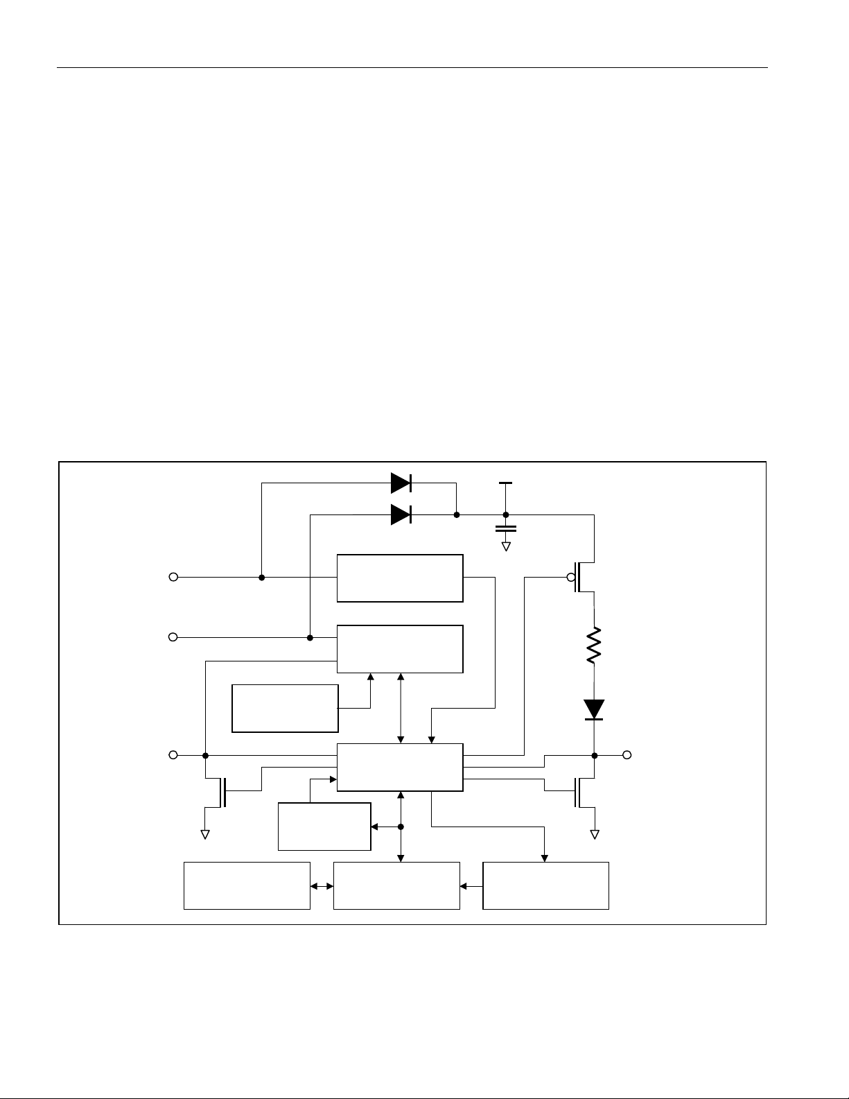
OVERVIEW
The block diagram in Figure 1 shows the relationships between the major function blocks of the DS28EA00. The
device has three main data components: 1) 64-bit Registration Number, 2) 64-bit scratchpad, and 3) alarm and
configuration registers. The 1-Wire ROM Function control unit processes the ROM function commands that allow
the device to function in a networked environment. The device function control unit implements the device-specific
control functions, such as read/write, temperature conversion, setting the chain state for sequence detection, and
PIO access. The CRC generator assists the master verifying data integrity when reading temperatures and
memory data. In the sequence detect process, PIOB functions as an input, while PIOA provides the connection to
the next device. The power supply sensor allows the master to remotely read whether the DS28EA00 has local
power available.
Figure 2 shows the hierarchical structure of the 1-Wire p rotocol. The bus master must first provide one o f the eight
ROM function commands: 1) Read ROM, 2) Match ROM, 3) Search ROM, 4) Conditional (“Alarm”) Search ROM,
5) Conditional Read ROM, 6) Skip ROM, 7) Overdrive-Skip ROM or 8) Overdrive-Match ROM. Upon completion of
an Overdrive ROM command byte executed at standard speed, the device enters Overdrive mode, where all
subsequent communication occurs at a higher speed. The protocol required for these ROM function commands is
described in Figure 12. After a ROM function command is successfully executed, the device-specific control
functions become accessible and the master may provide any one of the nine available commands. The protocol
for these control function commands is described in Figure 10. All data is read and written least significant bit
first.
Figure 1. DS28EA00 Block Diagram
Internal VDD
VDD
IO
64-Bit
Registration #
PIOB
EN\)
8-Bit CRC
Generator
Alarm and Config
Registers
Power Supply
Sensor
1-Wire ROM
Function Control
Device Function
Control
64-Bit Scratchpad
RCO
PIOA
DONE\)
Temperature
Sensor
5 of 29
Page 6

DS28EA00 1-Wire Digital Thermometer with Sequence Detect and PIO
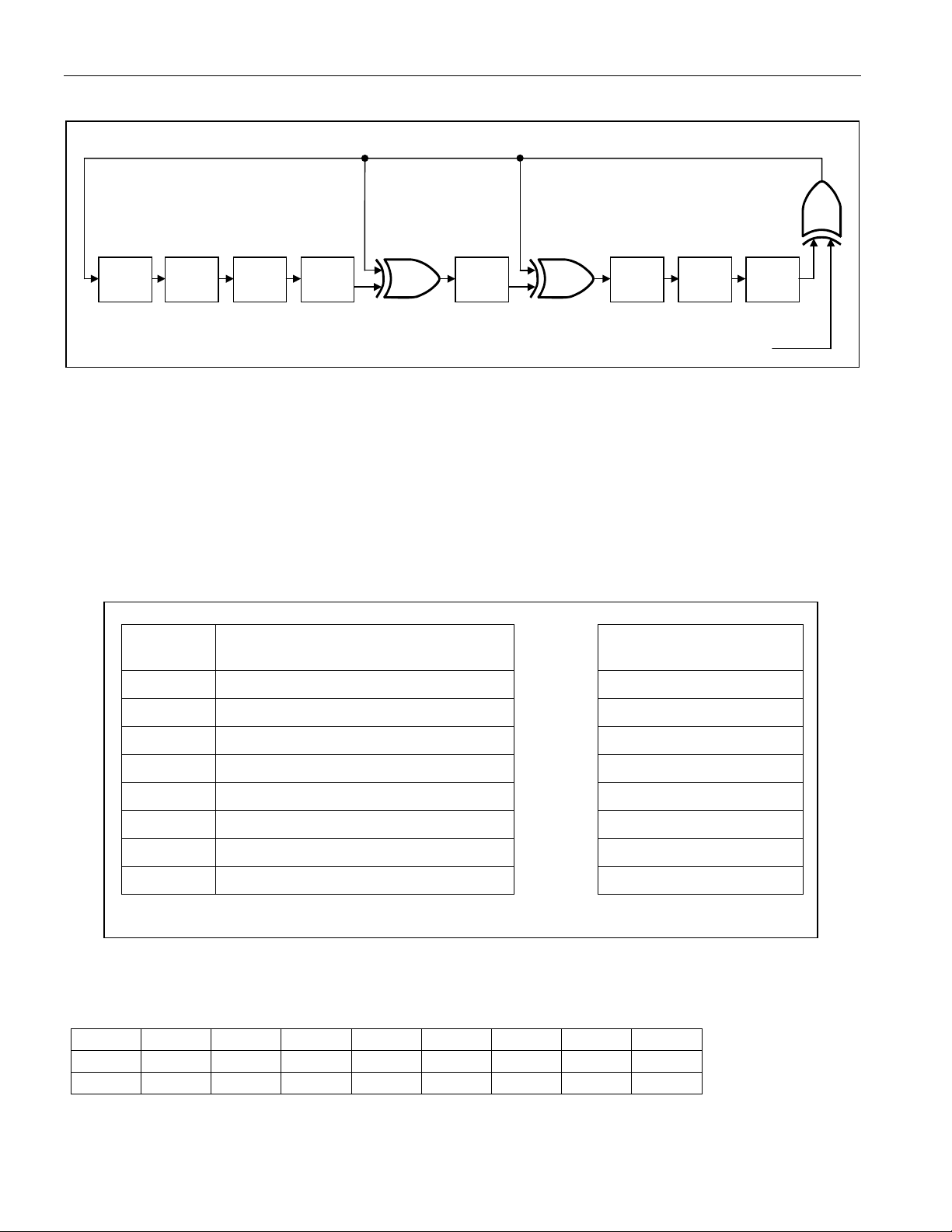
64-BIT REGISTRATION NUMBER
Each DS28EA00 contains a unique Registration Number that is 64 bits long. The first 8 bits are a 1-Wire family
code. The next 48 bits are a unique serial number. The last 8 bits are a CRC of the first 56 bits. See Figure 3 for
details. The 1-Wire CRC is generated using a polynomial generator consisting of a shift register and XOR gates as
shown in Figure 4. The polynomial is X
Redundancy Check (CRC) is available in Application Note 27.
The shift register bits are initialized to 0. Then starting with the least significant bit of the family code, one bit at a
time is shifted in. After the 8th bit of the family code has been entered, then the 48-bit serial number is entered.
After the last byte of the serial number has been entered, the shift register contains the CRC value. Shifting in the 8
bits of CRC returns the shift register to all 0s.
Figure 2. Hierachical Structure for 1-Wire Protocol
8
+ X5 + X4 + 1. Additional information about the Dallas 1-Wire Cyclic
DS28EA00
Command
Level:
1-Wire ROM Function
Commands (see Figure 12)
Device-Specific
Control Function
Commands (see Figure 10)
Available
Commands:
Read ROM
Match ROM
Search ROM
Conditional Search
ROM
Conditional Read
ROM
Skip ROM
Overdrive Skip
Overdrive Match
Write Scratchpad
Read Scratchpad
Copy Scratchpad
Convert Temperature
Read Power Mode
Recall EEPROM
PIO Access Read
PIO Access Write
Chain
Data Field
Affected:
64-bit Reg. #
64-bit Reg. #
64-bit Reg. #
64-bit Reg. #, Temperature Alarm
Registers, Scratchpad
64-bit Reg. #, PIOB pin state, Chain
state
(none)
64-bit Reg. #, OD-Flag
64-bit Reg. #, OD-Flag
Scratchpad
Scratchpad
Temperature Alarm and Configuration
Registers
Scratchpad, Temperature Alarm
Registers
V
pin voltage
DD
Scratchpad, Temperature Alarm and
Configuration Registers
PIO pins
PIO pins
Chain state, PIOA pin state
Figure 3. 64-Bit Registration Number
MSB LSB
8-Bit
CRC Code
MSB LSB MSB LSB MSB LSB
48-Bit Serial Number
8-Bit Family
Code (42h)
6 of 29
Page 7
DS28EA00 1-Wire Digital Thermometer with Sequence Detect and PIO
Figure 4. 1-Wire CRC Generator
Polynomial = X8 + X5 + X4 + 1
STAGE
0
X
st
1
STAGE
1
X
nd
2
2
X
rd
3
STAGE
STAGE
3
X
th
4
STAGE
4
X
th
5
5
X
th
6
STAGE
INPUT DATA
6
X
th
7
STAGE
STAGE
7
X
th
8
8
X
Memory Description
The memory of the DS28EA00 is shown in Figure 5. It consists of an 8-byte scratchpad and 3 bytes of backup
EEPROM. The first two bytes form the temperature readout register, which is updated after a temperature
conversion and is read-only. The next 3 bytes are user-writeable; they contain the Temperature High (TH) and the
Temperature Low (TL) alarm register and a configuration register. The remaining 3 bytes are “reserved”. They
power up with constant data and cannot be written by the user. The TH, TL, and configuration register da ta in the
scratchpad control the resolution of a temperature conversion and decide whether a temperature is considered as
“alarming”. TH, TL, and configuration can be copied to the EEPROM to become nonvolatile (NV). The scratchpad
is automatically loaded with EEPROM data when the DS28EA00 powers up.
Figure 5. Memory Map
BYTE
ADDRESS
0 Temperature LSB (50h) N/A
1 Temperature MSB (05h) N/A
SCRATCHPAD (POWER-UP STATE) BACKUP EEPROM
2 TH Register or User Byte 1* <--------> TH Register or User Byte 1
3 TL Register or User Byte 2* <--------> TL Register or User Byte 2
4 Configuratio n Register* <--------> Configuration Register
5 Reserved (FFh) N/A
6 Reserved (0Ch) N/A
7 Reserved (10h) N/A
*Power-up state depends on value(s) stored in EEPROM.
Register Detailed Description
Temperature Readout Register
ADDR bit 7 bit 6 bit 5 bit 4 bit 3 bit 2 bit 1 bit 0
0 23 2
2
2
1 S S S S S 26 2
1
2
0
2
-1
2
-2
2
-3
2
5
2
-4
4
LS Byte
MS Byte
7 of 29
Page 8

DS28EA00 1-Wire Digital Thermometer with Sequence Detect and PIO
The temperature reading is in °C using a 16-bit sign-extended two’s complement format. Table 1 shows examples
of temperature and the corresponding data for 12-bit resolution. With two’s complement, the sign bit is set if the
value is negative. If the device is configured for 12-bit resolution, all bits in the LS byte are valid; for a reduced
resolution, bit 0 (11 bit mode), bits 0 to 1 (10 bit mode), and bits 0 to 2 (9 bit mode) are undefined.
Table 1. Temperature/Data Relationship
TEMPERATURE
DIGITAL OUTPUT
(BINARY)
DIGITAL OUTPUT
(HEX)
+85°C* 0000 0101 0101 0000 0550h
+25.0625°C 0000 0001 1001 0001 0191h
+10.125°C 0000 0000 1010 0010 00A2h
+0.5°C 0000 0000 0000 1000 0008h
0°C 0000 0000 0000 0000 0000h
-0.5°C 1111 1111 1111 1000 FFF8h
-10.125°C 1111 1111 0101 1110 FF5Eh
-25.0625°C 1111 1110 0110 1111 FE6Fh
-40°C 1111 1101 1000 0000 FD80h
*The power-on r es et v a lu e of t he t e mperat ure readout register is +85°C.
Temperature Alarm Registers
ADDR bit 7 bit 6 bit 5 bit 4 bit 3 bit 2 bit 1 bit 0
2 S 26 2
3 S 26 2
5
2
5
2
4
2
4
2
3
2
3
2
2
2
2
2
1
2
1
2
0
0
High Alarm (TH)
Low Alarm (TL)
The result of a temperature conversion is automatically compared to the values in the alarm registers to determine
whether an alarm condition exists. Alarm thresholds are represented as two’s complement number. With 8 bits
available for sign and value, alarm thresholds can be set in increments of 1°C. An alarm condition exists if a
temperature conversion results in a value that is either higher than or equal to the value stored in the TH register
or lower than or equal to the value stored in the TL register. If a temperature alarm condition exists, the device
will respond to the Conditional Search command. The alarm condition is cleared if a subsequent temperature
conversion results in a temperature reading within the boundaries defined by the data in the TH and TL registers.
Configuration Register
ADDR b7 b6 b5 b4 b3 b2 b1 b0
4 0 R1 R0 1 1 1 1 1
The functional assignments of the individual bits are explained in the table below. Bits 0 to 4 and bit 7 have no
function; they cannot be changed by the user. As a factory default, the device operates in 12-bit resolution.
BIT DESCRIPTION BIT(S) DEFINITION
R0, R1: Temperature
Converter Resolution
b5, b6
These bits control the resolution of the temperature
converter. The codes are as follows:
R1 R0
0 0 9 bits
0 1 10 bits
1 0 11 bits
1 1 12 bits
8 of 29
Page 9
DS28EA00 1-Wire Digital Thermometer with Sequence Detect and PIO
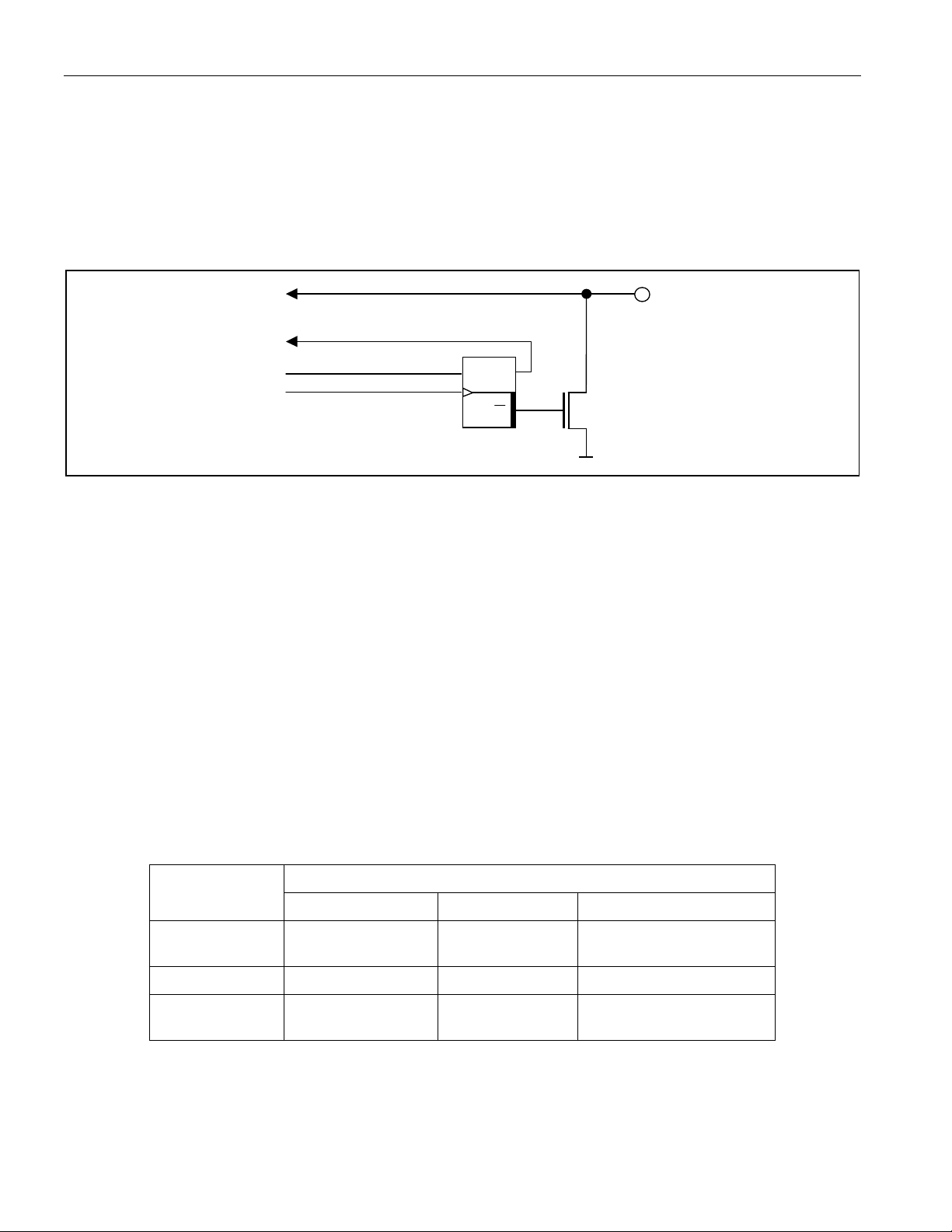
PIO Structure
Each PIO consists of an open-drain pulldown transistor and an input path to read the pin state. The transistor is
controlled by the PIO Output Latch, as shown in Figure 6. The Device Function Control unit connects the PIOs
logically to the 1-Wire interface. PIOA has a pullup path to internal V
to facilitate the sequence detect function
DD
(see Figure 1) in conjunction with the Chain command; PIOB is truely an open-drain structure. The power-on
default state of the PIO output transistors is off; high-impedance on-chip resistors (not shown in the graphic) pull
the PIO pins to internal V
DD
.
Figure 6. PIO Simplified Logic Diagram
PIO Pin
State
PIO Output
Latch State.
PIO Pin
PIO Data
PIO Clock
CLOCK
QD
Q
PIO Output Latch
Chain Function
The chain function is a feature that allows the 1-Wire master to discover the physical sequence of devices that are
wired as a linear network (“chain”). This is particularly convenient for devices that are installed at equal spacing
along a long cable, e.g., to measure temperatures at different locations inside a storage tower or tank. Without
chain function, the master needs a lookup table to correlate registration number to the physical location.
The chain function requires two pins, an input (EN\) to enable a device to respond during the discovery and an
output (DONE\) to inform the next device in the chain that the discovery of its neighbor is done. The two general
purpose ports of the DS28EA00 are re-used for the chain function. PIOB functions as EN\ input and PIOA
generates the DONE\ signal, which is connected to the EN\ input of the next device, as shown in the typical
operating circuit on page 1. The EN\ input of the first device in the chain needs to be hardwired to GND or logic ‘0’
must be applied for the duration of the sequence discovery process. Besides the two pins, the sequence discovery
relies on the Conditional Read ROM command.
For the chain function and normal PIO operation to coexist, the DS28EA00 distinguishes three chain states, OFF,
ON, and DONE. The transition from one chain state to another is controlled through the Chain command. Table 2
summarizes the chain states and the specific behavior of the PIO pins.
Table 2. Chain States
CHAIN STATE
DEVICE BEHAVIOR
PIOB (EN\) PIOA (DONE\) Conditional Read ROM
OFF (default)
ON
DONE
PIO (high
impedance)
EN\ input Pullup on Recognized if EN\ is ‘0’
No function
PIO (high
impedance)
Pulldown on ( DO \
logic ‘0’)
Not recognized
Not recognized
The power-on default chain state is OFF, where PIOA and PIOB are solely controlled through the PIO Access
Read and Write commands. In the chain ON state PIOA is pulled high to the device’s internal V
supply through a
DD
~40kΩ resistor, applying a logic ‘1’ to the PIOB (EN\) pin of the next device. Only in the ON state does a
DS28EA00 respond to the Conditional Read ROM command, provided its EN\ is at logic ‘0’. After a device’s ROM
9 of 29
Page 10

DS28EA00 1-Wire Digital Thermometer with Sequence Detect and PIO
Registration number is read, it is put into the chain DONE state, which enables the next device in the chain to
respond to the Conditional Read ROM command.
At the beginning of the sequence discovery process all devices are put into the chain ON state. As the discovery
progresses, one device after another is transitioned into the DONE state until all devices are identified. Finally, all
devices are put into the chain OFF state, which releases the PIOs and restores their power-on default state.
CONTROL FUNCTION COMMANDS
The Control Function Flow Chart (Figure 10) describes the protocols necessary for measuring temperatures,
accessing the memory and PIOs, and changing the chain state. Examples on how to use these and other functions
are included at the end of this document. The communication between master and DS28EA00 takes place either at
standard speed (default, OD = 0) or at Overdrive Speed (OD = 1). If not explicitly set into the Overdrive mode after
power-up the DS28EA00 communicates at standard speed.
WRITE SCRATCHPAD [4Eh]
This command allows the master to write 3 bytes of data to the scratchpad of the DS28EA00. The first data byte is
associated with the TH register (byte address 2), the second byte is associated with the TL register (byte address
3), and the third byte is associated with the configuration register (byte address 4). Data must be transmitted least
significant bit first. All three bytes MUST be written before the master issues a reset, or the data may be corrupted.
READ SCRATCHPAD [BEh]
This command allows the master to read the contents of the scratchpad. The data transfer starts with the least
significant bit of the temperature readout register at byte address 0 and continues through the remaining 7 bytes of
the scratchpad. If the master continues reading, it gets a 9
th
byte, which is an 8-bit CRC of all the data in the
scratchpad. This CRC is generated by the DS28EA00 and uses the same polynomial function as is used with the
ROM Registration Number. The CRC is transmitted in its true (non-inverted) form. The master may issue a reset to
terminate the reading early if only part of the scratchpad data is needed.
COPY SCRATCHPAD [48h]
This command copies the contents of the scratchpad byte addresses 2 to 4 (TH, TL and configuration registers) to
the back-up EEPROM. If the device has no V
for the duration of t
PROGMAX
within 10µs after this command is issued. If the device is powered through the VDD pin,
power, the master must enable a strong pullup on the 1-Wire bus
DD
the master may generate read time slots to monitor the copy process. Copy is completed when the master reads 1bits instead of 0-bits.
CONVERT TEMPERATURE [44h]
This command initiates a temperature conversion. Following the conversion, the resulting thermal data is found in
the temperature readout register in the scratchpad and the DS28EA00 returns to its low-power idle state. If the
device has no V
ble resolution-dependent t
V
pin, the master may generate read time slots to monitor the conversion process. The conversion is completed
DD
power, the master must enable a strong pullup on the 1-Wire bus for the duration of the applica-
DD
CONVMAX
within 10µs after this command is issued. If the device is powered through the
when the master reads 1-bits instead of 0-bits.
READ POWER MODE [B4h]
For Copy Scratchpad and Convert Temperature the master needs to know whether the DS28EA00 has VDD power
available. The Read Power Mode command is implemented to provide the master with this information. After the
command code, the master issues read time slots. If the master reads 1’s, the device is powered through the V
pin. If the device is powered through the 1-Wire line, the master will read 0’s. The power supply sensor samples the
state of the V
pin for every time slot that the master generates after the command code.
DD
DD
10 of 29
Page 11

DS28EA00 1-Wire Digital Thermometer with Sequence Detect and PIO
RECALL EEPROM [B8h]
This command recalls the TH and TL alarm trigger values and configuration data from backup EEPROM into their
respective locations in the scratchpad. After having transmitted the command code, the master may issue read
time slots to monitor the completion of the recall process. Recall is completed when the master reads 1-bits instead
of 0-bits. The recall occurs automatically at power-up, not requiring any activity by the master.
PIO ACCESS READ [F5h]
This command reads the PIO logical status and reports it together with the state of the PIO Output Latch in an
endless loop. A PIO Access Read can be terminated at any time with a 1-Wire Reset. PIO Access Read can be
executed in the Chain ON and Chain DONE state. While the device is in Chain ON or Chain DONE state, the PIO
output latch states will always read out as 1s; the PIO pin state may not be reported correctly.
PIO Status Bit Assignment
b7 b6 b5 b4 b3 b2 b1 b0
Complement of b3 to b0
The state of both PIO channels is sampled at the same time. The first sampling occurs during the last (most
significant) bit of the command code F5h. The PIO status is then reported to the bus master. While the master
receives the last (most significant) bit of the PIO status byte, the next sampling occurs and so on until the master
generates a 1-Wire Reset. The sampling occurs with a delay of t
previous byte, as shown in Figure 7. The value of "x" is approximately 0.2µs.
PIOB Output
Latch State
Figure 7. PIO Access Read Timing Diagram
PIOB Pin
State
PIOA Output
Latch State
+ x from the rising edge of the MS bit of the
REH
PIOA Pin
State
MS 2 bits of
previous byte
V
TH
IO
t
+x
REH
Sampling Point
Notes:
1 The "previous byte" could be the comma nd code or the data byte resulting from the previous PIO sample.
2 The sample point timing also applies to the PIO Access Write command, with the "previous byte" being the
write confirmation byte (AAh).
LS 2 bits of PIO
Status byte
PIO ACCESS WRITE [A5h]
The PIO Access Write command writes to the PIO output latches, which control the pulldown transistors of the PIO
channels. In an endless loop this command first writes new data to the PIO and then reads back the PIO status.
This implicit read-after-write can be used by the master for status verification. A PIO Access Write can be terminated at any time with a 1-Wire Reset. The PIO Access Write command is ignored by the device while in Chain ON
or Chain DONE state.
PIO Output Data Bit Assignment
b7 b6 b5 b4 b3 b2 b1 b0
X X X X X X PIOB PIOA
11 of 29
Page 12

DS28EA00 1-Wire Digital Thermometer with Sequence Detect and PIO
After the command code the master transmits a PIO Output Data byte that determines the new state of the PIO
output transistors. The first (least significant) bit is associated to PIOA; the next bit affects PIOB. The other 6 bits of
the new state byte do not have corresponding PIO pins. These bits should always be transmitted as "1"s. To switch
the output transistor on, the corresponding bit value is 0. To switch the output transistor off (non-conducting) the bit
must be 1. This way the bit transmitted as the new PIO output state arrives in its true form at the PIO pin. To
protect the transmission against data errors, the master must repeat the PIO Output Data byte in its inverted form.
Only if the transmission was error-free will the PIO status change. The actual PIO transition to the new state occurs
with a delay of t
of "x" is approximately 0.2µs. To inform the master about the successful communication of the PIO byte, the
DS28EA00 transmits a confirmation byte with the data pattern AAh. While the MS bit of the confirmation byte is
transmitted, the DS28EA00 samples the state of the PIO pins, as shown in Figure 7, and sends it to the master.
The master can either continue writing more data to the PIO or issue a 1-Wire Reset to end the command.
+ x from the rising edge of the MS bit of the inverted PIO byte, as shown in Figure 8. The value
REH
Figure 8. PIO Access Write Timing Diagram
MS 2 bits of inverted
PIO Output Dat a byte
V
t
REH
TH
+x
IO
PIO
LS 2 bits of confirmation byte (AAh)
CHAIN COMMAND [99h]
This command allows the master to put the DS28EA00 into one of the three Chain States, as shown in Figure 9.
The device powers up in the Chain OFF state. To transition a DS28EA00 from one state to another, the master
must send a suitable Chain Control byte after the Chain Command code. Only the codes 3Ch, 5Ah and 96h (true
form) are valid, assigned to OFF, ON, and DONE, in this sequence. This control byte is firs t transmitted in its true
form and then in its inverted form. If the Chain state change was successful, the master receives AAh confirmation
bytes. If the change was not successful (control byte transmission error, invalid control byte) the master will read
00h bytes instead.
Figure 9. Chain State Transition Diagram
Power-on
Reset (POR)
Chain ON
OFF
Chain DONE
Chain OFF
or POR
Chain DONE
ON DONE
Chain ON
These transitions are permissible, but
do not occur during normal operation.
12 of 29
Page 13

DS28EA00 1-Wire Digital Thermometer with Sequence Detect and PIO
Figure 10-1. Control Function Flow Chart
Bus Master TX Control
Function Command
Write Scratch-
Y
DS28EA00 sets
byte address = 2
Master TX data
byte to scratchpad
Master
TX Reset?
4Eh
pad?
N
Y
N
From ROM Functions
Flow Chart (Figure 12)
BEh
Read Scratch-
pad?
Y
DS28EA00 sets
byte address = 0
Master RX byte
from scratchpad
Master
TX Reset?
N
Byte
Address = 7?
N
Y
Y
To Figure 10
nd
Part
2
Byte
Address = 4?
N
DS28EA00 incre-
ments byte address
N
Master
TX Reset?
Y
Y
DS28EA00 incr e -
ments byte address
To ROM Functions
Flow Chart (Figure 12)
N
Master RX 8-bit
CRC of data
Master
TX Reset?
N
Master RX “1s“
Y
From Figure 10
2
nd
Part
13 of 29
Page 14

DS28EA00 1-Wire Digital Thermometer with Sequence Detect and PIO
Figure 10-2. Control Function Flow Chart (continued)
From Figure 10
st
Part
1
DS28EA00 starts
copy to EEPROM
Copy
Completed?
Master RX “0s“
Copy Scratch-
Y
N
48h
pad?
Y
VDD
Powered?
Y
N
Master decision
The master needs to
know whether V
power is available.
N
Master activates
strong pull-up
PROG
for t
DS28EA00 copies
scratchpad data
to EEPROM
Master deactivates
strong pull-up
Convert Tempera-
.
DD
Y
DS28EA00 starts
Temperature
Conversion
Conversion
Completed?
N
Master RX “0s“
44h
ture
Y
VDD
Powered?
Y
To Figure 10
rd
N
Part
3
N
Master activates
strong pull-up
CONV
for t
DS28EA00
converts
Temperature
Master deactivates
strong pull-up
To Figure 10
st
Part
1
Master
TX Reset?
N
Master RX “1s“
Y
Master
TX Reset?
N
Master RX “1s“
Y
From Figure 10
rd
Part
3
14 of 29
Page 15

DS28EA00 1-Wire Digital Thermometer with Sequence Detect and PIO
Figure 10-3. Control Function Flow Chart (continued)
From Figure 10
nd
Part
2
Y
Master RX “1s“
B4h
Read Power
Mode?
Y
VDD
Powered?
N
N
Master RX “0s“
B8h
Recall
EEPROM?
Y
DS28EA00 starts
Recall EEPROM
to Scratchpad
Recall
Completed?
N
Master RX “0s“
Master RX “1s“
N
Y
To Figure 10
th
Part
4
Master
TX Reset?
N
Y
Master
Y
TX Reset?
N
Master RX “1s“
To Figure 10
nd
Part
2
From Figure 10
th
Part
4
15 of 29
Page 16

DS28EA00 1-Wire Digital Thermometer with Sequence Detect and PIO
)1)
Figure 10-4. Control Function Flow Chart (continued)
From Figure 10
rd
3
Part
Note 1)
See the command
description for the
exact timing of the
PIO pin sampling
and updating.
Samples PIO Pin
F5h
PIO Access
Read?
Y
DS28EA00
N
1)
A5h
PIO Access
Write?
Y
Bus Master TX new
PIO Output Data Byte
Bus Master TX
inverted new PIO
Output Data Byte
Transmission
OK?
Y
DS28EA00
Updates PIO
Bus Master RX
Confirmation AAh
N
N
Bus Master
To Figure 10
RX “1”s
5
th
Part
To Figure 10
rd
3
Part
Bus Master RX
PIO Pin Status
Master
TX Reset?
Y
Y
N
DS28EA00
Samples PIO Pin
Bus Master RX
PIO Pin Status
N
Master
TX Reset?
Master
N
TX Reset?
1
Y
Y
From Figure 10
th
5
Part
16 of 29
Page 17

DS28EA00 1-Wire Digital Thermometer with Sequence Detect and PIO
Figure 10-5. Control Function Flow Chart (continued)
From Figure 10
th
Part
4
Valid Chain
Control Byte
Codes:
3Ch Off
5Ah On
96h Done
99h
Chain
Command?
Y
Master TX Ch ain
Control Byte
Master TX Inverted
Chain Control Byte
Transmission
Error?
N
Control Byte
Valid?
Y
Y
N
N
Y
Error defined as:
repeated control
byte not equal to
inverted control byte
Master
TX Reset?
N
Master RX “1s“
DS28EA00 up-
dates chain state
Master RX
To Figure 10
th
4
Part
Master RX con-
firmation cod e AAh
N
Master
TX Reset?
Y
inverted chain
control byte
N
Master
TX Reset?
Y
Master RX
error code 00h
N
Master
TX Reset?
Y
17 of 29
Page 18

DS28EA00 1-Wire Digital Thermometer with Sequence Detect and PIO
1-Wire BUS SYSTEM
The 1-Wire bus is a system that has a single bus master and one or more slaves. In all instances the DS28EA00 is
a slave device. The bus master is typically a microcontroller. The discussion of this bus system is broken down into
three topics: hardware configuration, transaction sequence, and 1-Wire signaling (signal types and timing). The
1-Wire protocol defines bus transactions in terms of the bus state during specific time slots, which are initiated on
the falling edge of sync pulses from the bus master.
HARDWARE CONFIGURATION
The 1-Wire bus has only a single line by definition; it is important that each device on the bus be able to drive it at
the appropriate time. To facilitate this, each device attached to the 1-Wire bus must have open-drain or tri-state
outputs. The 1-Wire port of the DS28EA00 is open drain with an internal circuit equivalent to that shown in Figure
11.
A multidrop bus consists of a 1-Wire bus with multiple slaves attached. The DS28EA00 supports both a Standard
and Overdrive communication speed of 15.3kbps (max) and 125kbps (max), respectively. Note that legacy 1-Wire
products support a standard communication speed of 16.3kbps and Overdrive of 142kbps. The slightly reduced
rates for the DS28EA00 are a result of additional recovery times, which in turn were driven by a 1-Wire physical
interface enhancement to improve noise immunity. The value of the pullup resistor primarily depends on the
network size and load conditions. The DS28EA00 requires a pullup resistor of 2.2kΩ (max) at any speed.
The idle state for the 1-Wire bus is high. If for any reason a transaction needs to be suspended, the bus MUST be
left in the idle state if the transaction is to resume. If this does not occur and the bus is left low for more than 16µs
(Overdrive speed) or more than 120µs (standard speed), one or more devices on the bus may be reset.
Figure 11. Hardware Configuration
BUS MASTER
V
PUP
DS28EA00 1-Wire PORT
R
PUP
RX
TX
DATA
I
Open-Drain
Port Pin
RX = RECEIVE
TX = TRANSMIT
L
100Ω
MOSFET
RX
TX
TRANSACTION SEQUENCE
The protocol for accessing the DS28EA00 through the 1-Wire port is as follows:
Initialization
ROM Function Command
Control Function Command
Transaction/Data
INITIALIZATION
All transactions on the 1-Wire bus begin with an initialization sequence. The initialization sequence consists of a
reset pulse transmitted by the bus master followed by presence pulse(s) transmitted by the slave(s). The presence
pulse lets the bus master know that the DS28EA00 is on the bus and is ready to operate. For more details, see the
1-Wire Signaling section.
18 of 29
Page 19

DS28EA00 1-Wire Digital Thermometer with Sequence Detect and PIO
1-Wire ROM FUNCTION COMMANDS
Once the bus master has detected a presence, it can issue one of the eight ROM function commands that the
DS28EA00 supports. All ROM function commands are 8 bits long. A list of these commands follows (refer to the
flow chart in Figure 12).
READ ROM [33h]
This command allows the bus master to read the DS28EA00’s 8-bit family code, unique 48-bit serial number, and
8-bit CRC. This command can only be used if there is a single slave on the bus. If more than one slave is present
on the bus, a data collision occurs when all slaves try to transmit at the same time (open drain produces a wiredAND result). The resultant family code and 48-bit serial number result in a mismatch of the CRC.
MATCH ROM [55h]
The Match ROM command, followed by a 64-bit ROM sequence, allows the bus master to address a specific
DS28EA00 on a multidrop bus. Only the DS28EA00 that exactly matches the 64-bit ROM sequence responds to
the following Control Function command. All other slaves wait for a reset pulse. This command can be used with a
single or multiple devices on the bus.
SEARCH ROM [F0h]
When a system is initially brought up, the bus master might not know the number of devices on the 1-Wire bus or
their registration numbers. By taking advantage of the wired-AND property of the bus, the master can use a
process of elimination to identify the registration numbers of all slave devices. For each bit of the registration
number, starting with the least significant bit, the bus master issues a triplet of time slots . On the first slot, each
slave device participating in the search outputs the true value of its registration number bit. On the second slot,
each slave device participating in the search outputs the complemented value of its registration number bit. On the
third slot, the master writes the true value of the bit to be selected. All slave devices that do not match the bit
written by the master stop participating in the search. If both of the read bits are zero, the master knows that slave
devices exist with both states of the bit. By choosing which state to write, the bus master branches in the ROM
code tree. After one complete pass, the bus master knows the registration number of a single device. Additional
passes identify the registration numbers of the remaining devices. Refer to Application Note 187: 1-Wire Search
Algorithm for a detailed discussion, including an example. The Search ROM command does not reveal any
information about the location of a device in a network. If multiple DS28EA00 are wired as a linear network
(“chain”), the device location can be detected using Conditional Read ROM in conjunction with the Chain function.
CONDITIONAL SEARCH ROM [ECh]
The Conditional Search ROM command operates similarly to the Search ROM command except that only those
devices, which fulfill certain conditions, participates in the search. This function provides an efficient means for the
bus master to identify devices on a multidrop system that have to signal an important event. After each pass of the
conditional search that successfully determined the 64-bit ROM code for a specific device on the multidrop bus,
that particular device can be individually accessed as if a Match ROM had been issued, since all o ther devices will
have dropped out of the search process and will be waiting for a reset pulse. The DS28EA00 will respond to the
conditional search if a temperature alarm condition exists. For more details see Temperature Alarm Registers.
CONDITIONAL READ ROM [0Fh]
This command is used in conjunction with the Chain function to detect the physical sequence of devices in a linear
network (“chain”). A DS28EA00 responds to Conditional Read ROM if two conditions are met: a) the device is in
chain ON state, and b) the EN\ input (PIOB) is at logic ‘0’. This condition is met by exactly one device during the
sequence discovery process. Upon receiving the Conditional Read ROM command, this particular device transmits
its 64-bit registration numberA device in chain ON state, but with a logic ‘1’ level at EN\ does not respond to
Conditional Read ROM. See Sequence Discovery Procedure for more details on the use of Conditional Read ROM
and the Chain command.
19 of 29
Page 20

DS28EA00 1-Wire Digital Thermometer with Sequence Detect and PIO
SKIP ROM [CCh]
This command can save time in a single-drop bus system by allowing the bus master to access the control
functions without providing the 64-bit ROM code. If more than one slave is present on the bus and, for example, a
read command is issued following the Skip ROM command, data collision occurs on the bus as multiple slaves
transmit simultaneously (open-drain pulldowns produce a wired-AND result).
OVERDRIVE SKIP ROM [3Ch]
On a single-drop bus this command can save time by allowing the bus master to access the control functions
without providing the 64-bit ROM code. Unlike the normal Skip ROM command, the Overdrive Skip ROM sets the
DS28EA00 in the Overdrive mode (OD = 1). All communication following this command has to occur at Overdrive
speed until a reset pulse of minimum 480µs duration resets all devices on the bus to standard speed (OD = 0).
When issued on a multidrop bus, this command sets all Overdrive-supporting devices into Overdrive mode. To
subsequently address a specific Overdrive-supporting device, a reset pulse at Overdrive speed has to be issued
followed by a Match ROM or Search ROM command sequence. This speeds up the time for the search process. If
more than one slave supporting Overdrive is present on the bus and the Overdrive Skip ROM command is followed
by a Read command, data collision occurs on the bus as multiple slaves transmit simultaneously (open-drain
pulldowns produce a wired-AND result).
OVERDRIVE MATCH ROM [69h]
The Overdrive Match ROM command followed by a 64-bit ROM sequence transmitted at Overdrive Speed allows
the bus master to address a specific DS28EA00 on a multidrop bus and to simultaneously set it in Overdrive mode.
Only the DS28EA00 that exactly matches the 64-bit ROM sequence responds to the subsequent control function
command. Slaves already in Overdrive mode from a previous Overdrive Skip or successful Overdrive Match
command remain in Overdrive mode. All overdrive-capable slaves return to standard speed at the next Reset Pulse
of minimum 480µs duration. The Overdrive Match ROM command can be used with a single or multiple devices on
the bus.
20 of 29
Page 21

DS28EA00 1-Wire Digital Thermometer with Sequence Detect and PIO
d
t
Figure 12-1. ROM Funtions Flow Chart
From Control Functions
Flow Chart (Figure 10)
Bus Master TX ROM
Function Command
33h
Read ROM
Command?
Y
N
55h
Match ROM
Command?
Bus Master TX
Reset Pulse
OD
Reset Pulse?
Y
DS28EA00 TX
Presence Pulse
N
N
OD = 0
F0h
Search ROM
Command?
YY Y
From Figure 12, 2
N
ECh
n
Par
To Figure 12
nd
Part
2
Cond. Search
Command?
N
N
Temp. Alarm?
Y
DS28EA00 TX
Family Code
(1 Byte)
DS28EA00 TX
Serial Number
(6 Bytes)
DS28EA00 TX
CRC Byte
Master TX Bit 0
Bit 0
Match?
Y
Master TX Bit 1
Bit 1
Match?
Y
Master TX Bit 63
Bit 63
Match?
Y
DS28EA00 TX Bit 0
DS28EA00 TX Bit 0
Master TX Bit 0
N
N
Bit 0
Match?
Y
DS28EA00 TX Bit 1
DS28EA00 TX Bit 1
Master TX Bit 1
N
N
Bit 1
Match?
Y
DS28EA00 TX Bit 63
DS28EA00 TX Bit 63
Master TX Bit 63
N
N
Bit 63
Match?
Y
DS28EA00 TX Bit 0
DS28EA00 TX Bit 0
Master TX Bit 0
N
Bit 0
Match?
DS28EA00 TX Bit 1
DS28EA00 TX Bit 1
Master TX Bit 1
N
Bit 1
Match?
DS28EA00 TX Bit 63
DS28EA00 TX Bit 63
Master TX Bit 63
N
Bit 63
Match?
Y
Y
Y
To Figure 12
nd
Part
2
From Figure 12
nd
Part
To Control Functions Flow
Chart (Figure 10)
2
21 of 29
Page 22

DS28EA00 1-Wire Digital Thermometer with Sequence Detect and PIO
t
Figure 12-2. ROM Functions Flow Chart
To Figure 12, 1
From Figure 12
st
1
Part
0Fh
Cond. Read
ROM?
Y
Chain = ON?
Y
EN\ = LOW?
Y
DS28EA00 TX
Family Code
(1 Byte)
DS28EA00 TX
Serial Number
(6 Bytes)
s
Part
N
N
N
CCh
Skip ROM
Cmnd.?
Y
N
Master
TX Reset?
N
3Ch
OD Skip
ROM?
Y
OD = 1
Master
TX Reset ?
N
Y
N
Master TX Bit 0
Y
Master TX Bit 1
Master TX Bit 63
69h
OD Match
ROM?
Y
OD = 1
Bit 0
Match?
Y
Bit 1
Match?
Y
N
N
N
1)
OD = 0
1)
OD = 0
DS28EA00 TX
CRC Byte
Bit 63
Match?
N
1)
OD = 0
Y
From Figure 12
st
Part
1
To Figure 12
st
Part
1
1) The OD flag remains at 1 if the device was already at Overdrive
speed before the Overdrive Match ROM command was issued.
22 of 29
Page 23

DS28EA00 1-Wire Digital Thermometer with Sequence Detect and PIO
X
V
ε
1-Wire SIGNALING
The DS28EA00 requires strict protocols to ensure data integrity. The protocol consists of four types of signaling on
one line: Reset Sequence with Reset Pulse and Presence Pulse, Write-Zero, Write-One, and Read-Data. Except
for the Presence pulse, the bus master initiates all falling edges. The DS28EA00 can communicate at two different
speeds, standard speed, and Overdrive Speed. If not explicitly set into the Overdrive mode, the DS28EA00
communicates at standard speed. While in Overdrive Mode the fast timing applies to all waveforms.
To get from idle to active, the voltage on the 1-Wire line needs to fall from V
from active to idle, the voltage needs to rise from V
past the threshold VTH. The time it takes for the voltage to
ILMAX
make this rise is seen in Figure 13 as 'ε' and its duration depends on the pullup resistor (R
capacitance of the 1-Wire network attached. The voltage V
is relevant for the DS28EA00 when determining a
ILMAX
logical level, not triggering any events.
Figure 13 shows the initialization sequence required to begin any communication with the DS28EA00. A Reset
Pulse followed by a Presence Pulse indicates the DS28EA00 is ready to receive data, given the correct ROM and
Control Function command. If the bus master uses slew-rate control on the falling edge, it must pull down the line
for t
device to standard speed. If the DS28EA00 is in Overdrive Mode and t
remains in Overdrive Mode. If the device is in Overdrive Mode and t
+ tF to compensate for the edge. A t
RSTL
duration of 480µs or longer exits the Overdrive Mode, returning the
RSTL
RSTL
is between 80µs and 480µs, the device will
RSTL
reset, but the communication speed is undetermined.
Figure 13. Initialization Procedure “Reset and Presence Pulses”
below the threshold VTL. To get
PUP
) used and the
PUP
is no longer than 80µs, the device
MASTER TX “RESET PULSE” MASTER RX “PRESENCE PULSE”
t
MSP
V
IHMASTER
V
V
PUP
V
V
ILMA
TH
TL
0
t
tF
t
RSTL
t
PDH
PDL
t
RSTH
t
REC
RESISTOR MASTER DS28EA00
After the bus master has released the line it goes into receive mode. Now the 1-Wire bus is pulled to V
the pullup resistor, or in case of a DS2482-x00 or DS2480B driver, by active circuitry. When the threshold V
crossed, the DS28EA00 waits for t
detect a presenc e p ul s e, t he m a st e r m ust t est th e l og i c a l st at e of t he 1 - W ir e l ine at t
and then transmits a Presence Pulse by pulling the line low for t
PDH
.
MSP
The t
DS28EA00 is ready for data communication. In a mixed population network, t
window must be at least the sum of t
RSTH
PDHMAX
, t
PDLMAX
, and t
. Immediately after t
RECMIN
should be extended to minimum
RSTH
is expired, the
RSTH
480µs at standard speed and 48µs at Overdrive speed to accommodate other 1-Wire devices.
through
PUP
PDL
is
TH
. To
READ/WRITE TIME SLOTS
Data communication with the DS28EA00 takes place in time slots, which carry a single bit each. Write-time slots
transport data from bus master to slave. Read-time slots transfer data from slave to master. Figure 14 illustrates
the definitions of the write- and read-time slots.
All communication begins with the master pulling the data line low. As the voltage on the 1-Wire line falls below the
threshold V
during a write-time slot and how long data is valid during a read-time slot.
, the DS28EA00 starts its internal timing generator that determines when the data line is sampled
TL
23 of 29
Page 24

DS28EA00 1-Wire Digital Thermometer with Sequence Detect and PIO
X
ε
X
Master-To-Slave
For a write-one time slot, the voltage on the data line must have crossed the VTH threshold before the write-one
low time t
threshold until the write-zero low time t
data line should not exceed V
the DS28EA00 needs a recovery time t
Figure 14. Read/Write Timing Diagram
Write-One Time Slot
is expired. For a write-zero time slot, the voltage on the data line must stay below the VTH
W1LMAX
is expired. For the most reliable communication, the voltage on the
W0LMIN
V
V
IHMASTER
V
ILMAX
PUP
V
V
TH
during the entire t
ILMAX
before it is ready for the next time slot.
REC
t
W1L
TL
W0L
or t
window. After the VTH threshold has been crossed,
W1L
0V
t
F
ε
t
SLOT
Write-Zero Time Slot
V
PUP
V
IHMASTER
V
TH
V
TL
V
ILMA
0V
t
F
RESISTOR MASTER
Read-Data Time Slot
V
PUP
V
IHMASTER
V
TH
V
TL
V
ILMA
0V
t
F
RESISTOR MASTER
t
W0L
t
SLOT
tRL
t
MSR
Master
Sampling
Window
δ
t
SLOT
t
REC
t
REC
RESISTOR MASTER DS28EA00
Slave-To-Master
A read-data time slot begins like a write-one time slot. The voltage on the data line must remain below VTL until the
read low time t
line low; its internal timing generator determines when this pulldown ends and the voltage starts rising again. When
responding with a 1, the DS28EA00 does not hold the data line low a t all, and the voltage starts rising as soon as
t
is over.
RL
is expired. During the tRL window, when responding with a 0, the DS28EA00 starts pulling the data
RL
24 of 29
Page 25

DS28EA00 1-Wire Digital Thermometer with Sequence Detect and PIO
The sum of t
define the master sampling window (t
For the most reliable communication, t
but no later than t
guarantees sufficient recovery time t
specified herein applies only to a single DS28EA00 attached to a 1-Wire line. For multidevice configurations, t
+ δ (rise time) on one side and the internal timing generator of the DS28EA00 on the other side
RL
. After reading from the data line, the master must wait until t
MSRMAX
to t
MSRMIN
should be as short as permissible, and the master should read close to
RL
for the DS28EA00 to get ready for the next time slot. Note that t
REC
) in which the master must perform a read from the data line.
MSRMAX
is expired. This
SLOT
REC
REC
needs to be extended to accommodate the additional 1-Wire device input capacitance. Alternatively, an interface
that performs active pullup during the 1-Wire recovery time such as the DS2482-x00 or DS2480B 1-Wire line
drivers can be used.
IMPROVED NETWORK BEHAVIOR (SWITCHPOINT HYSTERESIS)
In a 1-Wire environment, line termination is possible only during transients controlled by the bus master (1-Wire
driver). 1-Wire networks, therefore, are susceptible to noise of various origins. Depending on the physical size and
topology of the network, reflections from end points and branch points can add up, or cancel each other to some
extent. Such reflections are visible as glitches or ringing on the 1-Wire communication line. Noise coupled onto the
1-Wire line from external sources can also result in signal glitching. A glitch during the rising edge of a time slot can
cause a slave device to lose synchronization with the master and, consequently, result in a search ROM command
coming to a dead end or cause a device-specific function command to abort. For better performance in network
applications, the DS28EA00 uses a new 1-Wire front end, which makes it less sensitive to noise and also reduces
the magnitude of noise injected by the slave device itself.
The 1-Wire front end of the DS28EA00 differs from traditional slave devices in four characteristics.
1) The falling edge of the presence pulse has a controlled slew rate. This provides a better match to the line
impedance than a digitally switched transistor, converting the high frequency ringing known from traditional
devices into a smoother low-bandwidth transition. The slew rate control is specified by the parameter t
which has different values for standard and Overdrive speed.
2) There i s additional low-pass filtering in the circuit that detects the falling edge at the beginning of a time slot.
This reduces the sensitivity to high-frequency noise. This additional filtering does not apply at Overdrive speed.
3) There is a hysteresis at th e low-to-high switching threshold V
below V
- VHY, it will not be recognized (Figure 15, Case A). The hysteresis is effective at any 1-Wire speed.
TH
4) There is a time window specified by the rising edge hold-off time t
they extend below V
appear late after crossing the V
- VHY threshold (Figure 15, Case B, tGL < t
TH
threshold and extend beyond the t
TH
taken as the beginning of a new time slot (Figure 15, Case C, t
. If a negative glitch crosses VTH but does not go
TH
during which glitches are ignored, even if
REH
). Deep voltage droops or glitches that
REH
window cannot be filtered out and are
REH
≥ t
REH
).
GL
Devices that have the parameters V
and t
HY
specified in their electrical characteristics use the improved 1-Wire
REH
front end.
Figure 15. Noise Suppression Scheme
FPD
,
t
V
PUP
V
TH
REH
t
REH
VHY
Case A Case C Case B
0V
t
GL
tGL
25 of 29
Page 26

DS28EA00 1-Wire Digital Thermometer with Sequence Detect and PIO
Y
SEQUENCE DISCOVERY PROCEDURE
Precondition: The PIOB pin (EN\) of the first device in the chain is at logic 0. The PIOA pin (DONE\) of the first
device connects to the PIOB of the second device in the chain, etc., as shown in Figure 16. The 1-Wire master
detects the physical sequence of the devices in the chain by performing the following procedure:
Starting Condition: The master issues a Skip ROM command followed by a Chain ON command, which puts all
devices in the Chain ON state. The pullup through R
logic ‘1’ level at all devices except for the first device in the chain. If a local VDD supply is not available, the master
needs to activate a low-impedance bypass to the 1-Wire pullup resistor immediately after the inverted chain control
byte until the PIOA/PIOB connections have reached a voltage equivalent to the logic ‘1’ level.
First Cycle: The master sends a Conditional Read ROM command, which causes the first device in the chain to
respond with its 64-bit Registration Number. The master memorizes the Registration Number and the fact that this
is the first device in the chain. Next the master transmits a Chain DONE command. Through the PIOA pin of the
just discovered device, this asserts logic 0 at the PIOB pin of the second device in the chain and also prevents the
just discovered device from responding again.
Second Cycle: The master sends a Conditional Read ROM command. Since DS28EA00 #2 is the only device in
the chain with a LOW level at PIOB it responds with its Registration Number. The master stores the registration
number with the sequence number of 2. Device #1 cannot respond since it is in Chain DONE state. Next the
master transmits a Chain DONE command.
Additional Cycles: To identify the Registration Numbers of the remaining devices and their physical sequence, the
master repeats the steps of Conditional Read ROM, and Chain DONE. If there is no response to Conditional
Read ROM, all devices in the chain are identified.
Ending Condition
At the end of the discovery process all devices in the chain are in the Chain DONE state. The master should end
the sequence discovery by issuing a Skip ROM command followed by a Chain OFF command. This puts all the
devices into the Chain OFF state, and transfers control of the PIOB and PIOA pins to the PIO Access Read and
Write function commands.
Figure 16. DS28EA00 Wired for Sequence Discovery (“Chain Function”)
V
DD
of the PIOA pin charges the PIOA/PIOB connections to
CO
1-Wire
Master
PX.
(Micro-
controller)
* Capacitance of the cabling between adjacent devices in the chain.
#1 #2
VDD
IO
DS28EA00
PIOB PIOA
GND
IO
DS28EA00
PIOB PIOA
VDD
GND
#3
VDD
IO
DS28EA00
PIOB PIOA
**
GND
26 of 29
Page 27

DS28EA00 1-Wire Digital Thermometer with Sequence Detect and PIO
COMMAND-SPECIFIC 1-Wire COMMUNICATION PROTOCOL—LEGEND
SYMBOL DESCRIPTION
RST 1-Wire Reset Pulse generated by master.
PD 1-Wire Presence Pulse generated by slave.
SELECT Command and data to satisfy the ROM function protocol.
SKIPR ROM Function Command "Skip ROM".
CDRR ROM Function Command "Conditional Read ROM".
WSP Command "Write Scratchpad".
RSP Command "Read Scratchpad".
CPSP Command "Copy Scratchpad".
CTEMP Command "Convert Temperature".
RPM Command "Read Power Mode".
RCLE Command "Recall EEPROM".
PIOR Command "PIO Access Read".
PIOW Command "PIO Access Write".
CHAIN Command "Chain".
<n bytes> Transfer of n bytes.
CRC Transfer of a CRC byte
<xxh> Transfer of a specific byte value “xx” (hexadecimal notation)
00 loop Indefinite loop where the master reads 00 bytes.
FF loop Indefinite loop where the master reads FF bytes.
AA loop Indefinite loop where the master reads AA bytes.
xx loop Indefinite loop where the slave transmits the inverted invalid control byte.
CONVERSION
PROGRAMMING
A temperature conversion takes place; activity on the 1-Wire bus is permitted only with
local V
Data transfer to Backup EEPROM; activity on the 1-Wire bus is permitted only with local
V
DD
supply.
DD
supply.
COMMAND-SPECIFIC 1-Wire COMMUNICATION PROTOCOL—COLOR CODES
Master to slave Slave to master Programming Conversion
WRITE SCRATCHPAD
RST PD Select WSP <3 bytes> RST PD
READ SCRATCHPAD
RST PD Select RSP <8 bytes> CRC FF loop
27 of 29
Page 28

DS28EA00 1-Wire Digital Thermometer with Sequence Detect and PIO
COPY SCRATCHPAD (PARASITE POWERED)
RST PD Select CPS Wait t
PROGMAX
FF loop
During the wait, the master should activate a lowimpedance bypass to the 1-Wire pullup resistor.
COPY SCRATCHPAD (LOCAL VDD POWERED)
RST PD Select CPS <00h> FF loop
The master reads 00h bytes until the write cycle is completed.
CONVERT TEMPERATURE (PARASITE POWERED)
RST PD Select CTEMP Wait t
CONVMAX
FF loop
During the wait, the master should activate a lowimpedance bypass to the 1-Wire pullup resistor.
CONVERT TEMPERATURE (LOCAL VDD POWERED)
RST PD Select CTEMP <00h> FF loop
The master reads 00h bytes until the conversion is completed.
READ POWER MODE (PARASITE POWERED)
RST PD Select RPM <00h>
READ POWER MODE (LOCAL VDD POWERED)
RST PD Select RPM <FFh>
RECALL EEPROM
RST PD Select RCLE <00h> FF loop
The master reads 00h bytes until the recall is completed.
PIO ACCESS READ
RST PD Select PIOR <PIO Status Byte>
Continues until master sends Reset Pulse
See the Command description for behavior if the
device is in Chain ON or Chain DONE state.
28 of 29
Page 29

DS28EA00 1-Wire Digital Thermometer with Sequence Detect and PIO
PIO ACCESS WRITE (SUCCESS)
RST PD Select PIOW <PIO Output data> <PIO Output data> <AAh> <PIO Status Byte>
Loop until master sends Reset Pulse
PIO ACCESS WRITE (INVALID DATA BYTE)
RST PD Select PIOW <PIO Output data> <invalid data byte> FF loop
The PIO Access Write command is ignored by the device while in Chain ON or Chain DONE state.
CHANGE CHAIN STATE (SUCCESS)
RST PD Select CHAIN <Chain Control Byte> <Chain Control Byte> AA loop
CHANGE CHAIN STATE (TRANSMISSION ERROR)
RST PD Select CHAIN <Any Byte>
< Byte ≠ inverted Previous byte>
00 loop
CHANGE CHAIN STATE (INVALID CONTROL BYTE)
RST PD Select CHAIN <Invalid Control Byte> <Inverted Previous Byte > xx loop
SEQUENCE DISCOVERY EXAMPLE
RST PD SKIPR CHAIN <5Ah> <A5h> Wait for chain to charge <AAh>
RST PD CDRR <Registration Number> CHAIN <96h> <69h> <AAh>
RST PD CDRR <Registration Number> CHAIN <96h> <69h> <AAh>
RST PD CDRR <8 bytes FFh>
No response, all devices have been discovered.
Put all devices into
Chain ON state.
Identify the first device and
put it into Chain DONE state.
Identify the next device and
put it into Chain DONE state.
Repeat this sequence until no
device responds.
RST PD SKIPR CHAIN <3Ch> <C3h> <AAh>
For the sequence discovery to function properly, the logic state at PIOB (EN\) must not change during the
transmission of the Conditional Read ROM command code, and, if the device responds, must stay at logic 0 until
the entire 64-bit Registration Number is transmitted.
Put all devices into Chain OFF state.
29 of 29
 Loading...