

PX.Y
µC
R
PUP
V
CC
IO V
CC
POL
P1
P0
GND
A0
A6
DS28E04 #1
IO V
CC
POL
P1
P0
GND
A0
A6
DS28E04 #7
RST1 RST 0
LED
PART
TEMP RANGE
PIN-PACKAGE
DS28E04S-100+
-40°C to +85°C
16 SO
16 SO
(2.5k pieces)
Commands, Registers, and Modes are capitalized for
DS28E04-100
Wire EEPROM with PIO
19-6134; Rev 12/11
4096-Bit Addressable 1-
GENERAL DESCRIPTION
The DS28E04-100 is a 4096-bit, 1-Wire® EEPROM
chip with seven address inputs. The address inputs
are directly mapped into the 1-Wire 64-bit Device ID
Number to easily enable the host system to identify
the physical location or functional association of the
DS28E04-100 in a multidevice 1-Wire network environment. The 4096-bit EEPROM array is configured
as 16 pages of 32 bytes with a 32 byte scratchpad to
perform write operations. EEPROM memory pages
can be individually write protected or put in EPROMemulation mode, where bits can only be changed
from a 1 to a 0 state. In addition to the memory, the
DS28E04-100 has two general-purpose I/O ports that
can be used for input or to generate level and/or
pulse outputs. Activity registers also capture port
activity for state change monitoring. The DS28E04100 communicates over the single-contact 1-Wire
bus. The communication follows the standard Maxim
1-Wire protocol.
APPLICATIONS
Autoconfiguration of Modular Systems such as
Central-Office Switches, Cellular Base Stations,
Access Products, Optical Network Units, and
PBXs
Accessory/PCB Identification
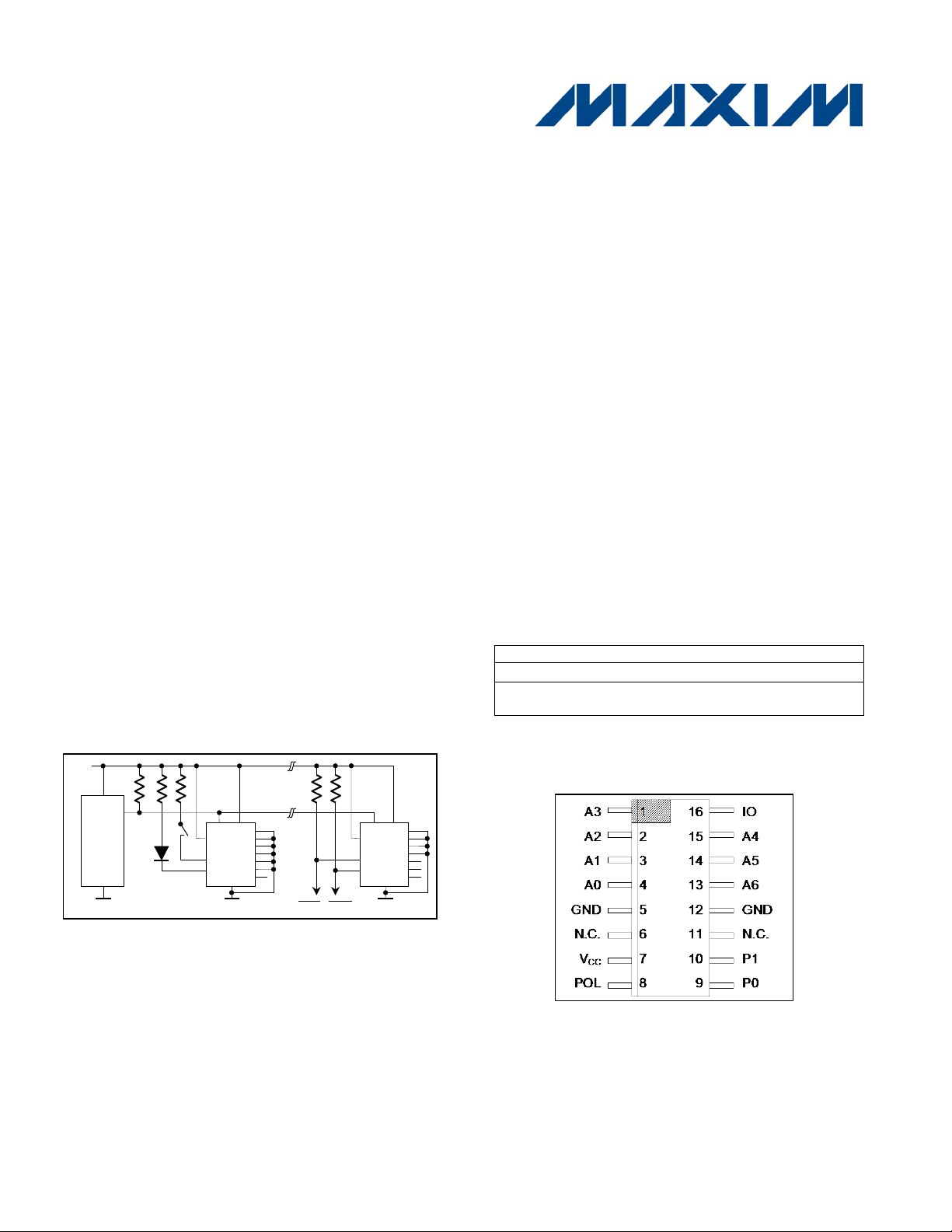
TYPICAL OPERATING CIRCUIT
FEATURES
• 4096 bits of EEPROM Memory Partitioned into
16 Pages of 256 Bits
• Seven Address Inputs for Physical Location
Configuration
• Two General-Purpose PIO Pins with Pulse-
Generation Capability
Individual Memory Pages can be Permanently
Write-Protected or put in OTP EPROMEmulation Mode (“Write to 0”)
Communicates to Host with a Single Digital
Signal at 15.3kbps or 111kbps Using 1-Wire
Protocol
Parasitic or V
Powered
CC
Conditional Search Based on PIO Status or PIO
Activity
Switchpoint Hysteresis and Filtering to Optimize
Performance in the Presence of Noise
Reads and Writes Over a Wide 2.8V to 5.25V
Voltage Range from -40°C to +85°C
16-Pin, 150-mil SO Package
ORDERING INFORMATION
DS28E04S-100+T -40°C to +85°C
+ Indicates lead(Pb)-free/RoHS-compliant package.
T = Tape and reel.
PIN CONFIGURATION
1 of 37
SO (150 mils)
clarity.
1-Wire is a registered trademark of Maxim Integrated Products, Inc.

DS28E04-100: 4096-Bit 1-Wire Addressable EEPROM with PIO
All Pins: Voltage to GND
-0.5V, +6V
All Pins: Sink Current
20mA
Operating Temperature Range
-40°C to +85°C
Junction Temperature
+150°C
Storage Temperature Range
-55°C to +125°C
Lead Temperature (soldering, 10s)
+300°C
Soldering Temperature (reflow)
+260°C
PARAMETER
SYMBOL
CONDITIONS
MIN
TYP
MAX
UNITS
Ground Current
I
GND
(Notes 1, 2, 3)
20
mA
Supply Current
I
CC
VCC = V
(Note 3)
1
mA
Standby Supply Current
I
CCS
Device idle; A0 to A6 not connected
11
µA
PINS A0 TO A6
Input Low Voltage
V
ILA
(Note 1)
0.30
V
VX -
0.3V
Input Load Current
I
LA
Pin at GND (Note 4)
-1.1
µA
POL PIN
Input Low Voltage
V
ILPOL
(Note 1)
0.30
V
VX -
0.3V
Leakage Current
I
LKPOL
Pin at 5.25V
1
µA
PIO PINS
Input Low Voltage
V
ILP
(Note 1)
0.30
V
VX -
0.3V
Output Low Voltage at
4mA
Leakage Current
I
LKP
Pin at 5.25V
1
µA
Minimum Sensed PIO
Pulse
Output Pulse Duration
t
PULSE
(Note 7)
250 1000
ms
IO PIN GENERAL DATA
1-Wire Pullup Resistance
R
PUP
(Notes 1, 8)
0.3 2.2
kΩ
Input Capacitance
CIO
(Notes 3, 9)
100
800
pF
IO pin at V
, A0 to A6 not connected,
V
CC
at GND
IO pin at V
, A0 to A6 not connected,
V
CC
at V
PUP
High-to-Low Switching
Threshold
Input Low Voltage
V
IL
(Notes 1, 12)
0.3
V
VX -
0.3V
Low-to-High Switching
Threshold
Switching Hysteresis
V
HY
(Notes 3, 10, 14)
0.21
1.70
V
Output Low Voltage
V
OL
At 4mA Current Load (Note 5)
0.4
V
Standard speed, R
PUP
= 2.2kΩ
5
Overdrive speed, R
PUP
= 2.2kΩ
2
Overdrive speed, directly prior to reset
pulse; R
PUP
= 2.2kΩ
Rising-Edge Hold-Off Time
(Note 3)
Standard speed (Note 16)
0.5 5.0
Overdrive speed
Not applicable (0)
ABSOLUTE MAXIMUM RATINGS
Stresses beyond those listed under “Absolute Maximum Ratings” may cause permanent damage to the device. These are stress ratings only,
and functional operation of the device at these or any other conditions beyond those indicated in the operational sections of the specifications is
not implied. Exposure to the absolute max imum rating conditions for extended periods may affect dev ice reliability.
ELECTRICAL CHARACTERISTICS
(V
= 2.8V to 5.25V, VCC = V
PUP
, not connected or grounded, TA = -40°C to +85°C.)
PUP
PUP
Input High Voltage V
Input High Voltage V
Input High Voltage V
V
t
PWM IN
Input Load Current I
IHA
IHPOL
IHP
OLP
VX = max(V
VX = max(V
VX = max(V
(Note 5) 0.4 V
, VCC) (Note 1)
PUP
, VCC) (Note 1)
PUP
, VCC) (Note 1)
PUP
V
V
V
(Note 6) 1 10 µs
PUP
L
V
TL
(Notes 3, 10, 11) 0.46 4.40 V
PUP
0.05 11.00
0.05 8.25
µA
Input High Voltage V
Recovery Time
(Notes 1, 15)
2 of 37
V
TH
t
REC
t
REH
IH
VX = max(V
, VCC) (Note 1)
PUP
V
(Notes 3, 10, 13) 1.0 4.9 V
µs
5
µs
DS28E04-100: 4096-Bit 1-Wire Addressable EEPROM with PIO
PARAMETER
SYMBOL
CONDITIONS
MIN
TYP
MAX
UNITS
Time Slot Duration
(Note 1)
Standard speed
65
Overdrive speed
9
IO PIN, 1-Wire RESET, PRESENCE DETECT CYCLE
Standard speed, V
PUP
> 4.5V
480 640
Standard speed (Note 17)
504 640
Overdrive speed, V
PUP
> 4.5V
48 80
Overdrive speed (Note 17)
53 80
Presence-Detect High
Time
Standard speed
15 60
Overdrive speed (Note 17)
2 7
Standard speed, V
PUP
> 4.5V
1.10
3.75
Standard speed
1.1 7.0
Overdrive speed
0 1.1
Standard speed
60 240
Overdrive speed, V
PUP
> 4.5V
8 24
Overdrive speed (Note 17)
8 26
Standard speed, V
PUP
> 4.5V
64 75
Standard speed
67 75
Overdrive speed
8.1 10
IO PIN, 1-Wire WRITE
Write-0 Low Time
(Notes 1, 19)
Standard speed
60 120
Overdrive speed (Note 17)
7 16
Write-1 Low Time
(Notes 1, 19)
Standard speed
5 15
Overdrive speed
1 2
IO PIN, 1-Wire READ
Read Low Time
(Notes 1, 20)
Standard speed
5
15 - δ
Overdrive speed
1
2 - δ
Read Sample Time
(Notes 1, 20)
Standard speed
tRL + δ 15
Overdrive speed
tRL + δ 2
EEPROM
Programming Current
I
PROG
(Note 21) 1 mA
Programming Time
t
PROG
(Note 22)
10
ms
Write/Erase Cycles
(Endurance) (Note 23)
At +25°C
200k
At +85°C (worst case)
50k
Data Retention
(Notes 23, 24)
Note 1:
System requir ement.
Note 2:
Maximum instantaneous pulldown current through all pins combined.
Note 3:
Guaranteed by design, simulation only. Not production tested.
Note 4:
This load current is caused by the internal weak pullup, which ass erts a logical 1 to address pins that are not connected. The
which these bits are relevant.
Note 5:
The I-V characteristic is linear for voltages less than 1V.
Note 6:
Width of the narrowest puls e that trips the activity latch. Back t o back pulses that are active for < t
(max) and that have an
intermediate inactive time < t
PWMIN
(max) are not guaranteed to be filtered.
Note 7:
The Puls e function requires that VCC power is available; otherwise the command will not be executed.
Note 8:
Maximum allowable pullup resistance is a function of the number of 1 -Wire devices in the system and 1-Wire recovery times. The
loaded s ystems, an active pullup such as that found in the DS2482-x00, DS2480B, or DS2490 may be required.
Note 9:
Capacitance on the data pin could be 800pF when V
is first applied. If a 2.2kΩ resistor is used to pull up the data line, 2.5µs
after V
PUP
has been applied the parasite capacitance will not aff ect normal communications.
Note 10:
VTL, VTH, and V
are a function of the internal supply voltage, which in parasit e power mode, is a function of V
and the 1-W ire
recovery times. The VTH and VTL maximum specifications are valid at VCC = V
PUP
= 5.25V. In any case, VTL < VTH < V
PUP
.
Note 11:
Voltage below which, during a falling edge on IO, a logic 0 is detected.
Note 12:
The voltage on IO needs to be less than or equal to V
ILM AX
whenever the master drives the line low.
Note 13:
Voltage above whic h, during a rising edge on IO, a logic 1 is detected.
Note 14:
After VTH is crossed dur ing a rising edge on IO, the voltage on IO has to drop by at least VHY to be detected as logic '0'.
Note 15:
Applies to a single DS28E04-100 without VCC supply, attached to a 1-Wire line.
Note 16:
The earliest recognition of a negative edge is possible at t
REH
after VTH has been previously reached.
Note 17:
Highlighted numbers are NOT in complianc e with legacy 1-W ire product standards. See comparison table.
Note 18:
Interval during the negative edge on IO at the beginning of a Presence Detect puls e between the time at which the voltage is
80% of V
PUP
and the time at which the voltage is 20% of V
PUP
.
Reset Low Time (Note 1) t
Presence-Detect Fall Time
(Notes 3, 18)
Presence-Detect Low
Time
Presence-Detect Sample
Time (Note 1)
t
SLOT
RSTL
t
PDH
t
FPD
t
PDL
t
MSP
t
W0L
t
W1L
t
RL
t
MSR
µs
µs
µs
µs
µs
µs
µs
µs
µs
µs
N
CY
tDR At +85°C (worst case) 40 years
logical state of the address pins must not change during the execution of ROM function commands during those time slots in
PWMIN
specified value here applies to systems with only one device and with the minimum 1-Wire recovery times. For more heavily
PUP
HY
PUP
3 of 37
DS28E04-100: 4096-Bit 1-Wire Addressable EEPROM with PIO
Note 19:
ε in Figur e 16 represents the time requir ed for the pullup circuitry to pull the voltage on IO up from VIL to VTH. The actual maximum
duration for the master to pull the line low is t
W1LMAX
+ tF - ε and t
W0LMAX
+ tF - ε respectively.
Note 20:
δ in Figure 16 represents the time requir ed for the pullup circuitry to pull the voltage on IO up from VIL to the input high threshold
of the bus master. T he actu al maximum duration for the master to pull the line low is t
RLM AX
+ tF.
Note 21:
Current drawn during the EEPROM programming interval. If the device does not get VCC power, the pullup circuit on IO during the
Vpup(min) then a low-impedance bypass of R
PUP
that can be activated during programming may need to be added.
Note 22:
The t
interval begins t
after the trailing rising edge on IO for the last time slot of the E/S byte for a valid C opy Scratchpad
device has returned from I
PROG
to IL or I
CCS
, r espectively.
Note 23:
Not production tested. Guaranteed by design or characterization.
Note 24:
EEPROM writes can become nonfunctional after the data-retention time is exceeded. Long-time storage at elevated temperatures
is not recommended; the device c an lose its write capability after 10 years at +125°C or 40 years at +85°C.
LEGACY VALUES
DS28E04-100 VALUES
PARAMETER
STANDARD SPEED
OVERDRIVE SPEED
STANDARD SPEED
OVERDRIVE SPEED
MIN
MAX
MIN
MAX
MIN
MAX
MIN
MAX
t
SLOT
(incl. t
REC)
61µs
(undef)
7µs
(undef)
65µs1)
(undef)
9µs
(undef)
t
RSTL
480µs
(undef)
48µs
80µs
504µs
640µs
53µs
80µs
t
PDH
15µs
60µs
2µs
6µs
15µs
60µs
2µs
7µs
t
PDL
60µs
240µs
8µs
24µs
60µs
240µs
8µs
26µs
t
W0L
60µs
120µs
6µs
16µs
60µs
120µs
7µs
16µs
PIN
NAME
FUNCTION
1
A3
Address bit input (place value = 8), with weak pullup.
2
A2
Address bit input (place value = 4), with weak pullup.
3
A1
Address bit input (place value = 2), with weak pullup.
4
A0
Least significant address bit input (place value = 1), with weak pullup.
5, 12
GND
Ground Reference
6, 11
N.C.
Not Connected
7
VCC
Optional power supply for the chip; leave unconnected or ground if VCC power
is not available.
8
POL
Power-up polarity (logical state) for P0 and P1; pin has a weak pulldown.
9
P0
Remote-controlled I/O pin, open drain with weak pulldown.
10
P1
Remote-controlled I/O pin, open drain with weak pulldown.
13
A6
Address bit input (place value = 64), with weak pullup.
14
A5
Address bit input (place value = 32), with weak pullup.
15
A4
Address bit input (place value = 16), with weak pullup.
16
IO
1-Wire Bus Interface. Open drain, requires external pullup resistor.
programming interval should be such that the voltage at IO is greater than or equal to V
PROG
sequence. Interval ends onc e the device's self-timed EEPRO M programming cycle is c omplete and the current drawn by the
REHmax
1)
Intentional change, longer recovery time requirement due t o modified 1-W ire front end.
PIN DESCRIPTION
(min). If V
PUP
in the system is close to
PUP
DETAILED DESCRIPTION
The DS28E04-100 combines 4096 bits of EEPROM, a 16-byte control page, two general-purpose PIO pins, seven
external address pins, and a fully featured 1-Wire interface in a single chip. PIO outputs are configured as opendrain and provide an on-resistance of 100Ω max. A robust PIO channel-access communication protocol ensures
that PIO output-setting changes occur error-free. The DS28E04-100 has an additional memory area called the
scratchpad that acts as a buffer when writing to the main memory or the control page. Data is first written to the
scratchpad from which it can be read back. The copy scratchpad command transfers the data to its final memory
location. Each DS28E04-100 has a device ID number that is 64 bits long. The user can define seven bits of this
number through address pins. The remaining 57 bits are factory-lasered into the chip. The device ID number
guarantees unique identification and is used to address the device in a multidrop 1-Wire network environment,
where multiple devices reside on a common 1-Wire bus and operate independently of each other. The DS28E04100 also supports 1-Wire conditional search capability based on PIO conditions or power-on-reset activity. The
DS28E04-100 has an optional V
parasitically from the 1-Wire bus. When an external supply is present, PIO states are maintained in the absence of
the 1-Wire bus power source. Applications of the DS28E04-100 include autoconfiguration and state monitoring of
modular systems such as central-office switches, cellular base stations, access products, optical network units, and
PBXs, and accessory/PC board identification.
supply connection. When an external supply is absent, device power is supplied
CC
4 of 37
DS28E04-100: 4096-Bit 1-Wire Addressable EEPROM with PIO
1-Wire Network
Device ID
Number Register
1-Wire
Function Control
Memory
Function
Control Unit
Special Function
Registers
32-
Byte
Scratchpad
Data Memory
16 Pages of
32 Bytes Each
CRC16
Generator
A0
A6
IO
Internal VDD
PIO
Control Registers
P0
VCC
P1
POL
Internal VDD
OVERVIEW
The block diagram in Figure 1 shows the relationships between the major control and memory sections of the
DS28E04-100. The DS28E04-100 has five main data components: 1) 64-bit device ID number, 2) 32-byte
scratchpad, 3) sixteen 32-byte pages of EEPROM, 4) Special Function Register, and 5) PIO Control Registers. The
hierarchical structure of the 1-Wire protocol is shown in Figure 2. The bus master must first provide one of the eight
ROM Function Commands, 1) Read ROM, 2) Match ROM, 3) Search ROM, 4) Conditional Search ROM, 5) Skip
ROM, 6) Resume, 7) Overdrive-Skip ROM or 8) Overdrive-Match ROM. Upon completion of an Overdrive ROM
command byte executed at standard speed, the device enters Overdrive mode where all subsequent
communication occurs at a higher speed. The protocol required for these ROM function commands is described in
Figure 14. After a ROM function command is successfully executed, the memory/control functions become
accessible and the master may provide any one of the nine Memory/Control Function commands. The protocol for
these commands is described in Figure 9. All data is read and written least significant bit first.
Figure 1. Block Diagram
5 of 37
DS28E04-100: 4096-Bit 1-Wire Addressable EEPROM with PIO
DS28E04-100
Available
Commands:
Command
Level:
Data Field
Affected:
1-Wire ROM Function
Commands (see Figure 14)
DS28E04
-Specific
Memory/Control Function
Commands (see Figure 9)
Read ROM
Match ROM
Search ROM
Conditional Search
ROM
Skip ROM
Resume
Overdrive Skip
Overdrive Match
Device ID, RC-Flag
Device ID, RC
-Flag
Device ID, RC-Flag
Device ID, RC-Flag, PIO Status,
cond. Search Settings
RC-Flag
RC-Flag
RC-Flag, OD-Flag
Device ID, RC-Flag, OD-Flag
Write Scratchpad
Read Scratchpad
Copy Scratchpad
Read Memory
PIO Access Read
PIO Access Write
PIO Access Pulse
Reset Act. Latch
Write Register
32-byte Scratchpad, Flags
32-byte Scratchpad
Data Memory, Register Page
Data Memory, Registers
PIO Pins
PIO Pins, Activity Latch
PIO Pins, Activity Latch
Activity Latch
Conditional Search and Control
Registers
MSB
LSB
8-Bit External
A6 A5 A4 A3 A2 A1 A
0
MSB LSB
MSB LSB
MSB LSB
MSB LSB
Figure 2. Hierarchical Structure for 1-Wire Protocol
64-BIT DEVICE ID NUMBER (NETWORK ADDRESS)
Each DS28E04-100 has a unique device ID number that is 64 bits long, as shown in Figure 3. The first 8 bits are a
1-Wire family code. The next 8 bits are an external address byte, of which the lower 7 bits are connected to the
address input pins A0 to A6. This allows the user to set a portion of the Device ID Number by connecting some of
these pins to GND (logic 0) or to V
number. Even if multiple DS28E04-100 are used in a 1-Wire network and all address inputs are wired to the same
state or left open (unconnected), the unique 40-bit serialization field will prevent any address conflict, allowing to
communicate with each device individually. The last 8 bits are a lasered CRC (Cyclic Redundancy Check) of the
first 56 bits, assuming that the address input pins A0 to A6 are at logic 1. The 1-Wire CRC is generated using a
polynomial generator consisting of a shift register and XOR gates as shown in Figure 4. The polynomial is X
4
X
+ 1. Further information on the Device ID CRC is found in section CRC Generation near the end of this
document.
Figure 3. 64-Bit Device ID Number
8-Bit CRC
Code
40-Bit Lasered Serial Number
(logic 1) or leaving them open (logic 1). The next 40 bits are a lasered serial
CC
8
+ X5 +
Address Input
0
8-Bit Family Code
(1Ch)
6 of 37
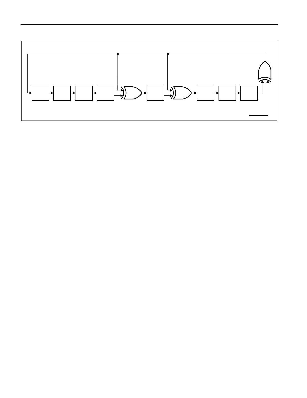
Figure 4. 1-Wire CRC Generator
X0X
1
X
2
X
3X4
X
5
X
6
X
7
X
8
Polynomial = X8 + X5 + X
4
+ 1
1
st
STAGE
2
nd
STAGE
3
rd
STAGE
4
th
STAGE
6
th
STAGE
5
th
STAGE
7
th
STAGE
8
th
STAGE
INPUT DATA
DS28E04-100: 4096-Bit 1-Wire Addressable EEPROM with PIO
MEMORY
The DS28E04-100 EEPROM array consists of 17 pages of 32 bytes each, starting at address 0000h and ending at
address 021Fh. All memory addresses in this range have unrestricted read access. The data memory consists of
16 pages of 32 bytes each. The register page consists of 32 bytes starting at address 0200h. It contains 16 page
protection control bytes (one for each data memory page), the register page lock byte, the factory bytes, and the
reserved bytes. The reserved bytes are for future use by the factory and should be not be used. They have no
effect on device operation.
The protection control registers, along with the register page lock byte, determine whether write protection, EPROM
mode, or copy protection is enabled for each of the 16 data memory pages. A value of 55h sets write protection for
the associated memory page. A value of AAh sets EPROM mode. A value of 55h or AAh for the register page lock
byte sets copy protection for all write-protected data memory pages, as well as the register page. EPROM mode
pages are not affected. The protection control registers and the register page lock byte write protect themselves if
set to 55h or AAh. Any other setting leaves them open for unrestricted write access.
In addition to the EEPROM, the device has a 32-byte volatile scratchpad. Writes to the EEPROM array are a twostep process. First, data is written to the scratchpad through the Write Scratchpad command, and then copied into
the main array through the Copy Scratchpad command. The user can verify the data written to the scratchpad
through the Read Scratchpad command prior to copying into the main array.
If a memory location is write protected, data sent by the master to the associated address during a Write
Scratchpad command is not loaded into the scratchpad. Instead, it is replaced by the data in EEPROM located at
the target address. If a memory location is in EPROM mode, the scratchpad is loaded with the logical AND of the
data sent by the master and the data in EEPROM at the target address. Copy Scratchpad commands to writeprotected or EPROM mode memory locations are allowed. This allows write-protected data in the device to be
refreshed, i.e., reprogrammed with the current data.
If a memory location is copy protected, a Copy Scratchpad command to that location will be blocked, which is
indicated by FFh success bytes. Copy protection is used for a higher level of security, and should only be used
after all write-protected pages and their associated protection control bytes are set to their final values. Copy
protection as implemented with this device does not prevent copying data from one device to another; it only blocks
the execution of the copy scratchpad command with a target address of a copy-protected memory page.
7 of 37

DS28E04-100: 4096-Bit 1-Wire Addressable EEPROM with PIO
Selection Mask
Figure 5. Memory Map
Address locations 0000h to 021Fh are nonvolatile. Address locations 0220h to 0225 are volatile.
ADDRESS RANGE TYPE DESCRIPTION PROTECTION CODES (NOTES)
0000h to 001Fh R/(W) Data Memory Page 0 (Protection controlled by address 0200h)
0020h to 003Fh R/(W) Data Memory Page 1 (Protection controlled by address 0201h)
0040h to 005Fh R/(W) Data Memory Page 2 (Protection controlled by address 0202h)
0060h to 007Fh R/(W) Data Memory Page 3 (Protection controlled by address 0203h)
0080h to 009Fh R/(W) Data Memory Page 4 (Protection controlled by address 0204h)
00A0h to 00BFh R/(W) Data Memory Page 5 (Protection controlled by address 0205h)
00C0h to 0DFh R/(W) Data Memory Page 6 (Protection controlled by address 0206h)
00E0h to 00FFh R/(W) Data Memory Page 7 (Protection controlled by address 0207h)
0100h to 011Fh R/(W) Data Memory Page 8 (Protection controlled by address 0208h)
0120h to 013Fh R/(W) Data Memory Page 9 (Protection controlled by address 0209h)
0140h to 015Fh R/(W) Data Memory Page 10 (Protection controlled by address 020Ah)
0160h to 017Fh R/(W) Data Memory Page 11 (Protection controlled by address 020Bh)
0180h to 019Fh R/(W) Data Memory Page 12 (Protection controlled by address 020Ch)
01A0h to 01BFh R/(W) Data Memory Page 13 (Protection controlled by address 020Dh)
01C0h to 01DFh R/(W) Data Memory Page 14 (Protection controlled by address 020Eh)
01E0h to 01FFh R/(W) Data Memory Page 15 (Protection controlled by address 020Fh)
0200h1) to 020Fh1) R/(W)
Protection Control Pages 0
to 15
0210h1) R/(W) Register Page Lock (See text)
0211h R Factory Byte (Reads 55h or AAh)
0212h to 021Dh N/A Reserved
021Eh to 021Fh R Factory Bytes (Undefined value)
55h: Write Protected; AAh: EPROM mode.
Address 0200h is associated with memory
page 0, address 0201h with page 1, etc.
220h R PIO Logic State (The lower two bits are valid)
221h R PIO Output Latch State (The lower two bits are valid)
222h R PIO Activity Latch State (The lower two bits are valid)
223h R/W2) Conditional Search PIO
224h R/W2) Conditional Search Polarity
225h R/W2) Conditional Search Control
1)
Once programmed to AAh or 55h this address becomes read-only. All other codes can be stored but will neither
write-protect the address nor activate any function.
2)
Limited write access through Write Register command
Selection
and Status Register
8 of 37
DS28E04-100: 4096-Bit 1-Wire Addressable EEPROM with PIO
PIO Output
Latch
PIO Activity
Latch
Edge
Detector
Port
Function
Control
To Activity Latch
State Register
To PIO Logic
State Register
To PIO Output
Latch State Reg.
R
Q D D
Q
Q
Q
"1"
CLR ACT LATCH
P0, P1
DATA
CLOCK
POWER ON
RESET
ADDR
b7
b6
b5
b4
b3
b2
b1
b0
0220h
1 1 1 1 1 1 P1
P0
ADDR
b7
b6
b5
b4
b3
b2
b1
b0
0221h
1 1 1 1 1 1 PL1
PL0
PIO-RELATED REGISTERS
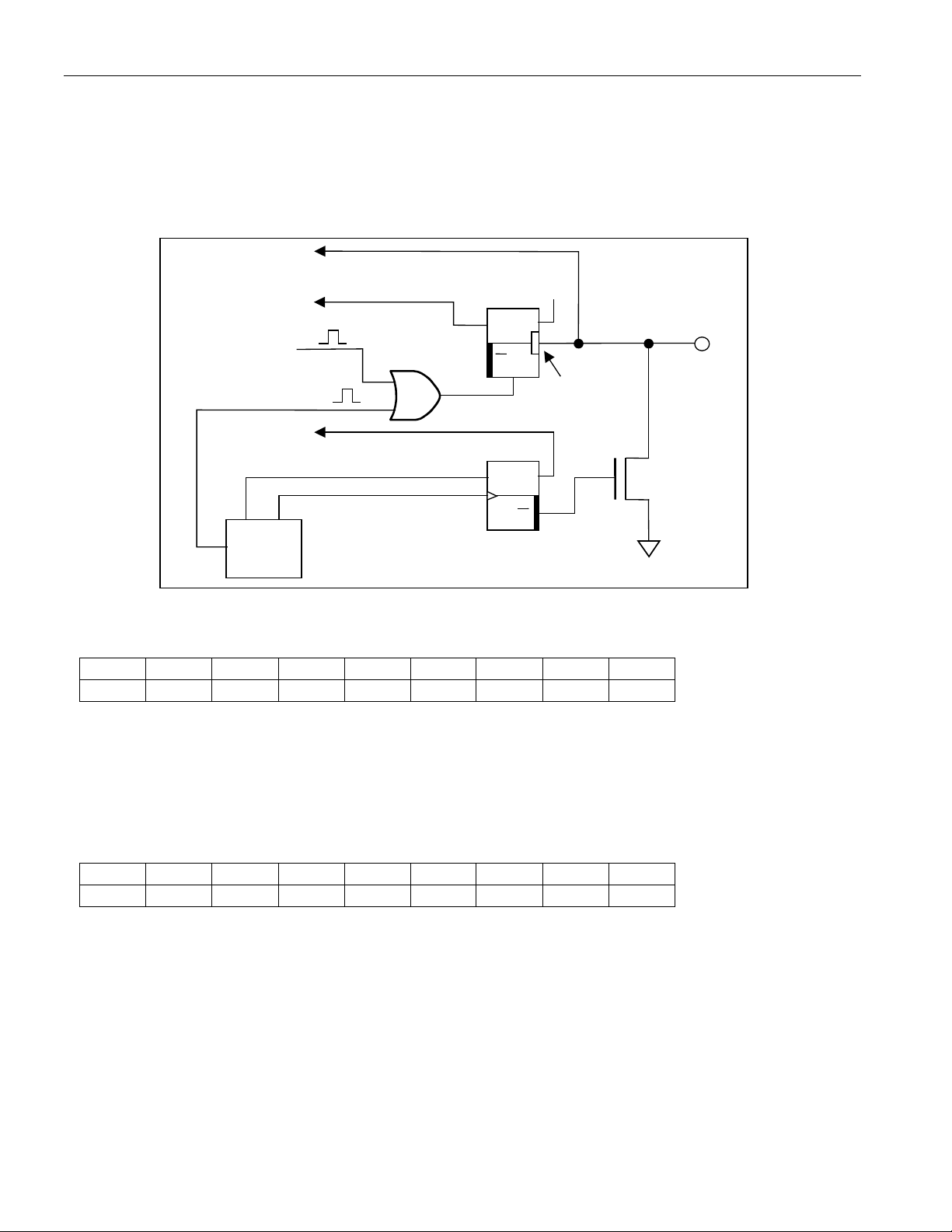
Figure 6 shows the simplified logic diagram of a PIO channel. The registers related to the PIO pins are located in
the address range 0220h to 0225h. All these registers are volatile, i.e., they lose their state when the device is
powered down. All PIO-related registers can be read like any data memory. There are special commands to control
the PIOs for input (read), output (write), pulse-generation, and to reset the activity latches.
Figure 6. PIO Simplified Logic Diagram
PIO Logic State Register
The logic state of the PIO pins can be obtained by reading this register using the Read Memory command. This
register is read-only. Each bit is associated with the pin of the respective PIO channel. Bits 2 to 7 have no function;
they always read 1. The data in this register reflects the PIO state at the last (most significant) bit of the byte that
proceeds reading the first (least significant) bit of this register. See the PIO Access Read command description for
details.
PIO Output Latch State Register
The data in this register represents the latest data written to the PIOs through the PIO Access Write command.
This register is read using the Read Memory command. This register is not affected if the device re-initializes itself
after an ESD hit. This register is read-only. Each bit is associated with the output latch of the respective PIO
channel. Bits 2 to 7 have no function; they always read 1. The flip-flops of this register power up as specified by the
state of the POL pin. If the chip has to power up with all PIO channels off, the POL pin must be connected to a logic
"1".
9 of 37
DS28E04-100: 4096-Bit 1-Wire Addressable EEPROM with PIO
ADDR
b7
b6
b5
b4
b3
b2
b1
b0
0222h
0 0 0 0 0 0 AL1
AL0
AL1
P1
PLS
SP0
SM0
CT
SM1
SP1
AL0
P0
CSR
Channel 0
Channel 1
PORL
ADDR
b7
b6
b5
b4
b3
b2
b1
b0
0223h
0 0 0 0 0 0 SM1
SM0
PIO Activity Latch State Register
The data in this register represents the current state of the PIO activity latches. This register is read using the Read
Memory command. This register is read-only. Each bit is associated with the activity latch of the respective PIO
channel. Bits 2 to 7 have no function; they always read 0. A state transition on a PIO pin, HighLow or
LowHigh, of a duration greater than t
causes the associated bit in the register to be set to a 1. This register
PW MI N
is cleared to 00h by a power-on reset, or by successful execution of the Reset Activity Latches command.
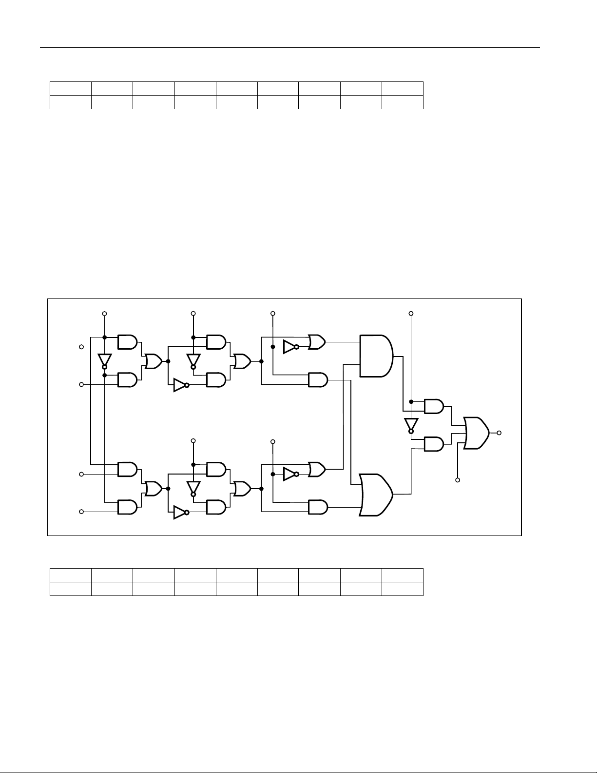
The next three registers control the device's participation a Conditional Search ROM sequence. The interaction of
the various signals that determine whether the device responds to a conditional search is illustrated in Figure 7.
There is a selection mask, SM, to select the participating PIOs, a polarity selection SP to specify for each channel
whether the channel signal needs to be 1 or 0 to qualify, and a PLS bit to select either the activity latches or PIO
pins as inputs. The signals of all channels are fed into an AND gate as well as an OR gate. The CT bit finally
selects the ANDed or ORed result as the conditional search response signal CSR. If CT is 0, the channel signal of
at least one of the selected channels must match the corresponding polarity. If CT is 1, the channel signals of all
selected channels must match the corresponding polarity.
Figure 7. CONDITIONAL SEARCH LOGIC
Conditional Search Channel Selection Mask Register
The data in this register controls whether a PIO channel qualifies for participation in the conditional search
command. To include a PIO channel, the bits in this register that correspond to those channels need to be set to 1.
This register can only be written through the Write Register command. This register is read/write. Each bit is
associated with the respective PIO channel as shown in Figure 7. Bits 2 to 7 have no function; they always read 0
and cannot be changed to 1. This register is cleared to 00h by a power-on reset.
10 of 37

DS28E04-100: 4096-Bit 1-Wire Addressable EEPROM with PIO
ADDR
b7
b6
b5
b4
b3
b2
b1
b0
0224h
0 0 0 0 0 0 SP1
SP0
ADDR
b7
b6
b5
b4
b3
b2
b1
b0
0225h
VCCP
POL 0 0
PORL
0
CT
PLS
BIT DESCRIPTION
BIT(S)
DEFINITION
1: activity latch selected
Specifies whether the data of two channels needs to be ORed or
1: bitwise AND
Search ROM sequence.
Reports the state of the POL pin. The state of the POL pin specifies
1: PIO powers up 1
1: VCC-powered operation
Conditional Search Channel Polarity Selection Register
The data in this register specifies the polarity of each selected PIO channel for the device to respond to the
conditional search command. This register can only be written through the W rite Registers command. Within a PIO
channel, the data source may be either the channel's input pin or the channel's activity latch, as specified by the
PLS bit in the Control/Status register at address 0225h. This register is read/write. Each bit is associated with the
respective PIO channel as shown in Figure 7. Bits 2 to 7 have no function; they always read 0 and cannot be
changed to 1. This register is cleared to 00h at power-up.
Control/Status Register
The data in this register reports status information and further configures the device for conditional search. This
register can only be written through the Write Registers command. This register is read/write. The power-up state
of the PORL bit is "1". CT and PLS power up as "0". The functional assignments of the individual bits are explained
in the table below. Bits 2, 4, and 5 have no function; they always read 0 and cannot be set to 1.
Control/Status Register Details
PLS: Pin or Activity
Latch Select
CT: Conditional Search
Logical Term
PORL: Power-On Reset
Latch
POL: PIO Default
Polarity (Read-Only)
VCCP: VCC Power
Status (Read-Only)
b0
b1
b3
b6
b7
Selects either the PIO pins or the PIO activity latches as input for the
conditional search.
0: pin selected (default)
AND’ed to meet the qualifying condition for the device to respond to
a conditional search. If only a single channel is selected in the
channel selection mask (0223h) this bit is a don't care.
0: bitwise OR (default)
Specifies whether the device has performed a power-on reset. This
bit can only be cleared to 0 by writing to the Control/Status Register.
As long as this bit is 1 the device will always respond to a Conditional
whether the PIO pins P0 and P1 power up high or low. The polarity
of a pulse generated at a PIO pin is the opposite of the pin's powerup state.
0: PIO powers up 0
For VCC-powered operation, the VCC pin needs to be connected to a
voltage source equal to V
0: V
power not available
CC
PUP
.
11 of 37

DS28E04-100: 4096-Bit 1-Wire Addressable EEPROM with PIO
Ending Address with
(Read Only)
ADDRESS REGISTERS AND TRANSFER STATUS
The DS28E04-100 employs three address registers, called TA1, TA2, and E/S (Figure 8). Registers TA1 and TA2
must be loaded with the target address to which the data will be written or from which data is read. Register E/S is
a read-only transfer-status register, used to verify data integrity of write commands. The lower five bits of the E/S
register indicate the Ending Offset within the 32-byte scratchpad. Bit 5 of the E/S register, called PF, is set if the
number of data bits sent by the master is not an integer multiple of 8 or if the data in the scratchpad is not valid due
to a loss of power. A valid write to the scratchpad clears the PF bit. Bit 6 has no function; it always reads 0. Note
that the lowest five bits of the target address also determine the address within the scratchpad, where intermediate
storage of data will begin. This address is called byte offset. If the target address (TA1) for a Write command is
03CH for example, then the scratchpad stores incoming data beginning at the byte offset 1CH and is full after only
four bytes. The corresponding ending offset in this example is 1FH. For maximum data bandwidth, the target
address for writing should point to the beginning of a new page, i.e., the byte offset is 0. Thus the full 32-byte
capacity of the scratchpad is available, resulting also in the ending offset of 1FH. However, it is possible to write
one or several contiguous bytes somewhere within a page. The ending offset together with the partial flag support
the master checking the data integrity after a Write command. The highest valued bit of the E/S register, called AA
is valid only if the PF flag reads 0. If PF is 0 and AA is 1, a copy has taken place. Writing data to the scratchpad
clears the AA flag.
Figure 8. Address Registers
Bit # 7 6 5 4 3 2 1 0
Target Address (TA1) T7 T6 T5 T4 T3 T2 T1 T0
Target Address (TA2) T15 T14 T13 T12 T11 T10 T9 T8
Data Status (E/S)
AA 0 PF E4 E3 E2 E1 E0
WRITING WITH VERIFICATION
To write data to the DS28E04-100 EEPROM sections, the scratchpad has to be used as intermediate storage. First
the master issues the Write Scratchpad command to specify the desired target address, followed by the data to be
written to the scratchpad. Under certain conditions (see Write Scratchpad command) the master will receive an
inverted CRC16 of the command, address (actual address sent), and data (as sent by the master) at the end of the
Write Scratchpad command sequence. Knowing this CRC value, the master can compare it to the value it has
calculated to decide whether the communication was successful and proceed to the Copy Scratchpad command. If
the master could not receive the CRC16, it should use the Read Scratchpad command to verify data integrity. As a
preamble to the scratchpad data, the DS28E04-100 repeats the target address TA1 and TA2 and sends the
contents of the E/S register. If the PF flag is set, data did not arrive correctly in the scratchpad or there was a loss
of power since data was last written to the scratchpad. The master does not need to continue reading; it can start a
new trial to write data to the scratchpad. Similarly, a set AA flag together with a cleared PF flag indicates that the
device did not recognize the Write command. If everything went correctly, both flags are cleared and the ending
offset indicates the address of the last byte written to the scratchpad. Now the master can continue reading and
verifying every data byte. After the master has verified the data, it can send the Copy Scratchpad command. This
command must be followed exactly by the data of the three address registers, TA1, TA2, and E/S. The master
should obtain the contents of these registers by reading the scratchpad.
12 of 37

DS28E04-100: 4096-Bit 1-Wire Addressable EEPROM with PIO
MEMORY/CONTROL FUNCTION COMMANDS
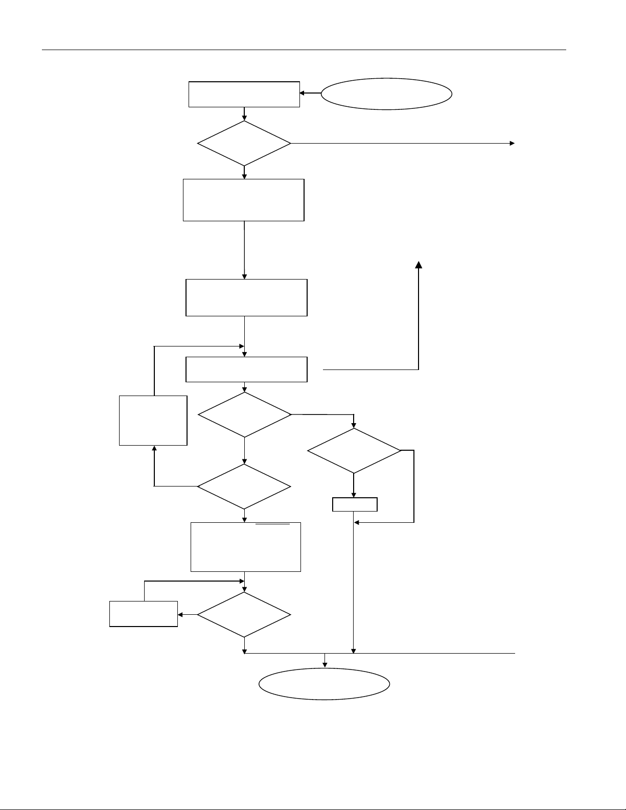
The Memory/Control Function Flow Chart (Figure 9) describes the protocols necessary to access the memory and
the PIO pins of the DS28E04-100. Examples on how to use these functions are included at the end of this
document. The communication between master and DS28E04-100 takes place either at standard speed (default,
OD = 0) or at Overdrive peed (OD = 1). If not explicitly set into the Overdrive Mode, the DS28E04-100 powers up in
standard speed.
WRITE SCRATCHPAD COMMAND [0Fh]
The Write Scratchpad command applies to the data memory, and the writeable addresses in the register page.
After issuing the Write Scratchpad command, the master must first provide the 2-byte target address, followed by
the data to be written to the scratchpad. The data is written to the scratchpad starting at the byte offset of T4:T0.
The ending offset (E4:E0) is the byte offset at which the master stops writing data. Only full data bytes are
accepted. If the last data byte is incomplete, its content will be ignored and the partial byte flag PF will be set.
When executing the Write Scratchpad command, the CRC generator inside the DS28E04-100 (Figure 18)
calculates a CRC of the entire data stream, starting at the command code and ending at the last data byte as sent
by the master. This CRC is generated using the CRC16 polynomial by first clearing the CRC generator and then
shifting in the command code (0FH) of the Write Scratchpad command, the Target Addresses (TA1 and TA2) as
supplied by the master, and all the data bytes. The master may end the Write Scratchpad command at any time.
However, if the end of the scratchpad is reached (E4:E0 = 11111b), the master can send 16 read-time slots and
receive the CRC generated by the DS28E04-100.
If a Write Scratchpad is attempted to a write-protected location, the scratchpad is loaded with the data already in
memory, rather than the data transmitted. Similarly, if the target address page is in EPROM mode, the scratchpad
is loaded with the bitwise logical AND of the transmitted data and data already in memory.
READ SCRATCHPAD COMMAND [AAh]
The Read Scratchpad command allows verification of the target address and the scratchpad data. After issuing the
command code, the master begins reading. The first two bytes are the target address. The next byte is the ending
offset/data status byte (E/S) followed by the scratchpad data, which may be different from what the master
originally sent. This is of particular importance if the target address is within the register page or a page in either
Write-Protected or EPROM modes. See the Write Scratchpad description for details. The master should read
E4:E0-T4:T0+1 bytes, after which it receives the inverted CRC16, based on data as it was sent by the DS28E04-
100. If the master continues reading after the CRC, all data will be logic 1s.
COPY SCRATCHPAD [55h]
The Copy Scratchpad command is used to copy data from the scratchpad to the data memory and the writable
sections of the Register Page. After issuing the Copy Scratchpad command, the master must provide a 3-byte
authorization pattern, which should have been obtained by an immediately preceding Read Scratchpad command.
This 3-byte pattern must exactly match the data contained in the three address registers (TA1, TA2, E/S, in that
order). If the pattern matches, the target address is valid, the PF flag is not set, and the target memory is not copyprotected, the AA (Authorization Accepted) flag is set and the copy begins. The data to be copied is determined by
the three address registers. The scratchpad data from the beginning offset through the ending offset will be copied
to memory, starting at the target address. Anywhere from 1 to 32 bytes can be copied with this command. The
device’s internal data transfer takes 10ms maximum during which the voltage on the 1-Wire bus must not fall below
2.8V. After waiting 10ms, the master may issue read time slots to receive AAh confirmation bytes until the master
issues a reset pulse. If the PF flag is set or the target memory is copy-protected, the copy will not begin and the AA
flag will not be set.
13 of 37
DS28E04-100: 4096-Bit 1-Wire Addressable EEPROM with PIO
0Fh
Write Scratch-
pad ?
Bus Master TX EEPROM
Array Target Address
TA1 (T7:T0), TA2 (T15:T8)
Y
N
To Figure 9
2nd Part
From Figure 9
2nd Part
Bus Master TX Memory
Function Command
To ROM Functions
Flow Chart (Figure 14)
From ROM Functions
Flow Chart (Figure 14)
Master
TX Reset ?
Master TX Data Byte
To Scratchpad Offset
N
Y
DS28E04 sets Scratchpad
Offset = (T4:T0),
Clears PF, AA
Scrpad. Offset
= 11111b?
DS28E04 TX CRC16
of Command, Address,
Data Bytes as they were
sent by the bus master
DS28E04
Increments
Scratchpad
Offset
Master
TX Reset ?
Y
N
Bus Master
RX “1”s
N
Partial
Byte ?
PF = 1
Y
N
Y
Applies only if the page is not write
protected or in EPROM mode. If writeprotected, then the DS28E04 copies the
data byte from the target address into
the scratchpad. If in EPROM mode,
then the DS28E04 stores the bitwise
logical AND of the transmitted byte and
the data byte from the targeted address
into the scratchpad.
Figure 9-1. Memory/Control Function Flow Chart
14 of 37

DS28E04-100: 4096-Bit 1-Wire Addressable EEPROM with PIO
AAh
Read Scratch-
Pad ?
DS28E04 sets Scratchpad
Offset = (T4:T0)
Bus Master RX
TA1 (T7:T0), TA2 (T15:T8)
and E/S Byte
Bus Master RX Data Byte
from Scratchpad Offset
Bus Master RX CRC16
of Command, Address,
E/S Byte, Data Bytes as
sent by the DS28E04
Y
Bus Master
RX “1”s
Master
TX Reset ?
Y
N
Master
TX Reset ?
DS28E04
Increments
Scratchpad
Offset
Scrpad. Offset
= E4:E0 ?
Y
Y
N
N
N
From Figure 9
1
st
Part
To Figure 9
1
st
Part
To Figure 9
3
rd
Part
From Figure 9
3
rd
Part
See note in Write
Scratchpad flow chart
for additional details.
Figure 9-2. Memory/Control Function Flow Chart (continued)
15 of 37

DS28E04-100: 4096-Bit 1-Wire Addressable EEPROM with PIO
From Figure 9
2nd Part
To Figure 9
2nd Part
To Figure 9
4th Part
From Figure 9
4th Part
* 1-Wire idle high 10ms for power
55h
Copy Scratch-
Pad ?
Bus Master TX
TA1 (T7:T0), TA2 (T15:T8)
and E/S Byte
Y
N
Bus Master
RX “1”s
Master
TX Reset ?
Y N Y
Auth. Code
Match ?
N
N
Copy-
Protected ?
Y
DS28E04 copies Scratch-
pad Data to Address
AA = 1
*
DS28E04 TX “0”
Master
TX Reset ?
Master
TX Reset ?
Y
N
DS28E04 TX “1”
N
Y
Applicable to all R/W
memory locations.
Y
T15:T0
< 0220h ?
N
PF = 0 ?
Y
N
Figure 9-3. Memory/Control Function Flow Chart (continued)
16 of 37

DS28E04-100: 4096-Bit 1-Wire Addressable EEPROM with PIO
Figure 9-4. Memory/Control Function Flow Chart (continued)
17 of 37

DS28E04-100: 4096-Bit 1-Wire Addressable EEPROM with PIO
Figure 9-5. Memory/Control Function Flow Chart (continued)
18 of 37

DS28E04-100: 4096-Bit 1-Wire Addressable EEPROM with PIO
Figure 9-6. Memory/Control Function Flow Chart (continued)
19 of 37

DS28E04-100: 4096-Bit 1-Wire Addressable EEPROM with PIO
IO
Example - Sampled State = FEh
MS 2 bits of
previous byte
LS 2 bits of
data byte (FEh)
V
TH
Sampling Point
t
REH
+x
READ MEMORY [F0h]
The Read Memory command is the general function to read data from the DS28E04-100. After issuing the
command, the master must provide a 2-byte target address in the range of 0000h to 0225h. After these two bytes,
the master reads data beginning from the target address and may continue until address 0225h. If the master
continues reading, the result will be logic 1s. The device's internal TA1, TA2, E/S, and scratchpad contents are not
affected by a Read Memory command.
The hardware of the DS28E04-100 provides a means to accomplish error-free writing to the memory section. To
safeguard reading data in the 1-Wire environment and to simultaneously speed up data transfers, it is
recommended to packetize data into data packets the size of one memory page each. Such a packet would
typically store a 16-bit CRC with each page of data to insure rapid, error-free data transfers that eliminate having to
read a page multiple times to determine if the received data is correct or not. (See Application Note 114 for the
recommended file structure.)
WRITE REGISTER [CCh]
The conditional search settings and the status/control register are volatile. They need to be loaded after every
power-up cycle with the Write Register command. After issuing the command, the master sends the 2-byte target
address, which should be a value between 0223h and 0225h. Next the master sends the byte to be written to the
addressed cell. If the address was valid, the byte is immediately written to its memory location. The master now
can either end the command by issuing a 1-Wire reset or send another byte for the next higher address. Once
memory address 0225h has been written, any subsequent data bytes will be ignored. The master has to send a
1-Wire reset to end the command. Since the Write Register flow does not include any error-checking for the new
register data, it is important to verify correct writing by reading the registers using the Read Memory command.
PIO ACCESS READ [F5h]
In contrast to reading the PIO logical state from address 0220h, this command reads the PIO logical status in an
endless loop. After 32 bytes of PIO pin status the DS28E04-100 inserts an inverted CRC16 into the data stream,
which allows the master to verify whether the data was received error-free. A PIO Access Read can be terminated
at any time with a 1-Wire Reset. The state of the POL pin does not affect this command.
The status of both PIO channels is sampled at the same time. The first sampling occurs during the last (most
significant) bit of the command code F5h. The first (least significant) bit of the PIO status byte is associated to P0,
and the next bit to P1. The other 6 bits of a PIO status byte do not have corresponding PIO pins; they always read
"1". While the master receives the last bit of the PIO status byte, the next sampling occurs and so on until the
master has received 32 PIO samples. Next the master receives the inverted CRC16 of the command byte and 32
PIO samples (first pass) or the CRC of 32 PIO samples (subsequent passes). While the last (most significant) bit of
the CRC is transmitted, the next PIO sampling takes place. The sampling occurs with a delay of t
rising edge of the MS bit of the previous byte, as shown in Figure 10. The value of "x" is approximately 0.2µs.
Figure 10. PIO Access Read Timing Diagram
+ x from the
REH
Notes:
1 The "previous byte" could be the command code, the data byte resulting from the previous PIO sample, or the
MS byte of a CRC16.
2 The sample point timing also applies to the PIO Access Write and Pulse command, with the "previous byte"
being the write confirmation byte (AAh).
20 of 37

DS28E04-100: 4096-Bit 1-Wire Addressable EEPROM with PIO
IO
PIO
Example - Old State =
MS 2 bits of inverted
new-state byte
LS 2 bits of confirmation byte (AAh)
FEh
FDh
V
TH
t
REH
+x
PIO ACCESS WRITE [5Ah]
The PIO Access Write command is the only way to write to the PIO output-latch state register (address 0221h),
which controls the open-drain output transistors of the PIO channels. In an endless loop, this command first writes
new data to the PIO and then reads back the PIO status. The implicit read-after-write can be used by the master for
status verification. A PIO Access Write can be terminated at any time with a 1-Wire Reset. The state of the POL pin
does not affect this command.
After the command code, the master transmits a byte that determines the new state of the PIO output transistors.
The first (least significant) bit is associated to P0; the next bit affects P1. The other 6 bits of the new state byte do
not have corresponding PIO pins. These bits should always be transmitted as "1"s. To switch the output transistor
off (nonconducting) the corresponding bit value is 1. To switch the transistor on, that bit needs to be 0. This way the
data byte transmitted as the new PIO output state arrives in its true form at the PIO pins. To protect the
transmission against data errors, the master must repeat the new PIO byte in its inverted form. Only if the
transmission was error-free does the PIO status change. The actual PIO transition to the new state occurs with a
delay of t
is approximately 0.2µs. To inform the master about the successful change of the PIO status, the DS28E04-100
transmits a confirmation byte with the data pattern AAh. After the MS bit of the confirmation byte is transmitted, the
DS28E04-100 samples the status of the PIO pins, as shown in Figure 10, and sends it to the master. Depending on
the data the master can either continue writing more data to the PIO or issue a 1-Wire reset to end the command.
Figure 11. PIO Access Write Timing Diagram
+ x from the rising edge of the MS bit of the inverted PIO byte, as shown in Figure 11. The value of "x"
REH
FEh, New state = FDh
PIO ACCESS PULSE [A5h]
As a convenient alternative to using PIO Access Write, the PIO Access Pulse command generates a self-timed
pulse on the selected PIO outputs. The polarity of the pulse is determined by the state of the POL pin. If POL = 1,
the pulse is negative (active low) and vice versa. The PIO Access Pulse command is accepted only if the device is
powered.
V
CC
After the command code the master transmits a selection mask that specifies the PIO at which the pulse is to be
generated. A PIO is selected if the corresponding bit in the selection mask is a "1". The first (least significant) bit is
associated to P0; the next bit affects P1. The other 6 bits of the selection mask do not have corresponding PIO
pins. These bits should always be transmitted as "1"s. To protect the transmission against data errors, the master
must repeat the selection mask in its inverted form. Only if the transmission was error-free does the pulse occur.
The pulse begins with a delay of t
+ x from the rising edge of the MS bit of the inverted selection mask, as
REH
shown in Figure 12. The value of "x" is approximately 0.2µs. To inform the master about the successful pulse
generation, the DS28E04-100 transmits a confirmation byte with the data pattern AAh. While the last bit of the
confirmation byte is transmitted, the DS28E04-100 samples the status of the PIO pins, as shown in Figure 10, and
sends it to the master. Now the master can issue a 1-Wire reset to exit the command flow. This does not terminate
the pulse on a PIO pin.
21 of 37

DS28E04-100: 4096-Bit 1-Wire Addressable EEPROM with PIO
t
PULSE
IO
PIO
MS 2 bits of inverted
Selection Mask
LS 2 bits of confirmation byte (AAh)
V
TH
t
REH
+x
POL=1
POL=0
Figure 12. PIO Access Pulse Timing Diagram
RESET ACTIVITY LATCHES [C3h]
Each PIO channel includes an activity latch that is set whenever there is a state transition at a PIO pin of duration
greater than t
. This change can be caused by an external event/signal or by writing to the PIO or by
PWMIN
generating a pulse. Depending on the application there may be a need to reset the activity latch after having
captured and serviced an external event. Since there is only read access to the PIO Activity Latch State Register,
the DS28E04-100 supports a special command to reset these latches. After having received the command code,
the device resets all activity latches simultaneously. There are two ways for the master to verify the execution of
the Reset Activity Latches command. One way is to start reading from the 1-Wire line right after the command code
is transmitted. In this case, the master reads AAh bytes until it sends a 1-Wire reset. The other way is reading
register address 0222h.
1-Wire BUS SYSTEM
The 1-Wire bus is a system that has a single bus master and one or more slaves. In all instances the DS28E04100 is a slave device. The bus master is typically a microcontroller. The discussion of this bus system is broken
down into three topics: hardware configuration, transaction sequence, and 1-Wire signaling (signal types and
timing). The 1-Wire protocol defines bus transactions in terms of the bus state during specific time slots, which are
initiated on the falling edge of sync pulses from the bus master.
HARDWARE CONFIGURATION
The 1-Wire bus has only a single line by definition; it is important that each device on the bus be able to drive it at
the appropriate time. To facilitate this, each device attached to the 1-Wire bus must have open-drain or tri-state
outputs. The 1-Wire port of the DS28E04-100 is open drain with an internal circuit equivalent to that shown in
Figure 13.
A multidrop bus consists of a 1-Wire bus with multiple slaves attached. The DS28E04-100 supports both a
standard and Overdrive communication speed of 15.4kbps (max) and 111kbps (max), respectively. Note that
legacy 1-Wire products support a standard communication speed of 16.3kbps and Overdrive of 142kbps. The
slightly reduced rates for the DS28E04-100 are a result of additional recovery times, which in turn were driven by a
1-Wire physical interface enhancement to improve noise immunity. The value of the pullup resistor primarily
depends on the network size and load conditions. The DS28E04-100 requires a pullup resistor of 2.2kΩ (max) at
any speed.
The idle state for the 1-Wire bus is high. If, for any reason, a transaction needs to be suspended, the bus MUST be
left in the idle state if the transaction is to resume. If this does not occur and the bus is left low for more than 16µs
(Overdrive speed) or more than 120µs (standard speed), one or more devices on the bus can be reset.
22 of 37

DS28E04-100: 4096-Bit 1-Wire Addressable EEPROM with PIO
Open-Drain
Port Pin
RX = RECEIVE
TX = TRANSMIT
100 Ω
MOSFET
V
PUP
RX
TX
TX
RX
DATA
R
PUP
11µA
Max.
BUS MASTER
DS28E04 1
-Wire PORT
Figure 13. Hardware Configuration
TRANSACTION SEQUENCE
The protocol for accessing the DS28E04-100 through the 1-Wire port is as follows:
Initialization
ROM Function Command
Memory/Control Function Command
Transaction/Data
INITIALIZATION
All transactions on the 1-Wire bus begin with an initialization sequence. The initialization sequence consists of a
reset pulse transmitted by the bus master followed by presence pulse(s) transmitted by the slave(s). The presence
pulse lets the bus master know that the DS28E04-100 is on the bus and is ready to operate. For more details, see
the 1-Wire Signaling section.
1-Wire ROM FUNCTION COMMANDS
Once the bus master has detected a presence, it can issue one of the eight ROM function commands that the
DS28E04-100 supports. All ROM function commands are 8 bits long. A list of these commands follows (refer to the
flow chart in Figure 14).
READ ROM [33h]
This command allows the bus master to read the DS28E04-100’s 8-bit family code, unique 40-bit serial number, 8bit address byte, and 8-bit CRC. The lower order 7 bits of the address byte read back the state of the address pins
A6 to A0. See also Figure 3. This command can only be used if there is a single slave on the bus. If more than one
slave is present on the bus, a data collision occurs when all slaves try to transmit at the same time (open drain
produces a wired-AND result). The resultant family code and 48-bit serial number result in a mismatch of the CRC.
Note that there will also be a CRC mismatch if one or more of the external address inputs are connected to GND.
The ROM CRC is hardcoded with A6 to A0 set to 1s. The master should comprehend this and calculate the ROM
CRC similarly.
MATCH ROM [55h]
The Match ROM command, followed by a 64-bit ROM sequence, allows the bus master to address a specific
DS28E04-100 on a multidrop bus. Only the DS28E04-100 that exactly matches the 64-bit ROM sequence,
including the external address, responds to the following Memory/Control Function command. All other slaves wait
for a reset pulse. This command can be used with a single or multiple devices on the bus.
23 of 37

DS28E04-100: 4096-Bit 1-Wire Addressable EEPROM with PIO
SEARCH ROM [F0h]
When a system is initially brought up, the bus master might not know the number of devices on the 1-Wire bus or
their device ID numbers. By taking advantage of the wired-AND property of the bus, the master can use a process
of elimination to identify the device ID numbers of all slave devices. For each bit of the device ID number, starting
with the least significant bit, the bus master issues a triplet of time slots. On the first slot, each slave device
participating in the search outputs the true value of its device ID number bit. On the second slot, each slave device
participating in the search outputs the complemented value of its device ID number bit. On the third slot, the master
writes the true value of the bit to be selected. All slave devices that do not match the bit written by the master stop
participating in the search. If both of the read bits are zero, the master knows that slave devices exist with both
states of the bit. By choosing which state to write, the bus master branches in the romcode tree. After one complete
pass, the bus master knows the device ID number of a single device. Additional passes identify the device ID
numbers of the remaining devices. Refer to Application Note 187: 1-Wire Search Algorithm for a detailed
discussion, including an example.
Note: Since the DS28E04-100 lasered ROM CRC is calculated assuming the address inputs are all logic 1, then
any address inputs that are connected to GND are not validated. It is recommended to do a double search when
building a list of devices on the 1-Wire line.
CONDITIONAL SEARCH [ECh]
The Conditional Search ROM command operates similarly to the Search ROM command except that only those
devices, which fulfill certain conditions (CSR = 1), will participate in the search. This function provides an efficient
means for the bus master to identify devices on a multidrop system that have to signal an important event. After
each pass of the conditional search that successfully determined the 64-bit ROM code for a specific device on the
multidrop bus, that particular device can be individually accessed as if a Match ROM had been issued, since all
other devices will have dropped out of the search process and will be waiting for a reset pulse. The DS28E04-100
responds to the conditional search if the CSR signal is active. See the description of the registers at addresses
0223h to 0225h and Figure 7 for more details.
SKIP ROM [CCh]
This command can save time in a single-drop bus system by allowing the bus master to access the memory
functions without providing the 64-bit ROM code. If more than one slave is present on the bus and, for example, a
Read command is issued following the Skip ROM command, data collision occurs on the bus as multiple slaves
transmit simultaneously (open-drain pulldowns produce a wired-AND result).
RESUME [A5h]
To maximize the data throughput in a multidrop environment, the Resume function is available. This function
checks the status of the RC bit and, if it is set, directly transfers control to the Memory functions, similar to a Skip
ROM command. The only way to set the RC bit is through successfully executing the Match ROM, Search ROM, or
Overdrive Match ROM command. Once the RC bit is set, the device can repeatedly be accessed through the
Resume Command function. Accessing another device on the bus clears the RC bit, preventing two or more
devices from simultaneously responding to the Resume Command function.
OVERDRIVE SKIP ROM [3Ch]
On a single-drop bus this command can save time by allowing the bus master to access the memory functions
without providing the 64-bit ROM code. Unlike the normal Skip ROM command, the Overdrive Skip ROM sets the
DS28E04-100 in the Overdrive mode (OD = 1). All communication following this command has to occur at
Overdrive speed until a reset pulse of minimum 480µs duration resets all devices on the bus to standard speed
(OD = 0).
When issued on a multidrop bus, this command sets all Overdrive-supporting devices into Overdrive mode. To
subsequently address a specific Overdrive-supporting device, a reset pulse at Overdrive speed has to be issued
followed by a Match ROM or Search ROM command sequence. This speeds up the time for the search process. If
more than one slave supporting Overdrive is present on the bus and the Overdrive Skip ROM command is followed
by a Read command, data collision occurs on the bus as multiple slaves transmit simultaneously (open-drain
pulldowns produce a wired-AND result).
24 of 37

DS28E04-100: 4096-Bit 1-Wire Addressable EEPROM with PIO
From Figure 14
2nd Part
To Memory Functions
Flow Chart (Figure 9)
Master TX Bit 0
Master TX Bit 63
Master TX Bit 1
RC = 1
DS28E04 TX
Family Code
(1 Byte)
Bit 0
Match?
Y
N
Bit 1
Match?
Y
N
Bit 63
Match?
Y
N
DS28E04 TX Bit 0
DS28E04 TX Bit 0
Master TX Bit 0
DS28E04 TX Bit 1
DS28E04 TX Bit 1
Master TX Bit 1
DS28E04
TX Bit 63
DS28E04
TX Bit 63
Master TX Bit 63
RC = 1
Bit 0
Match?
Y
N
Bit 1
Match?
Y
N
Bit 63
Match?
Y
N
To Figure 14
2
nd
Part
RC = 0
RC = 0
RC = 0
RC = 0
Y Y Y
Y
N
F0h
Search ROM
Command?
N
55h
Match ROM
Command?
N
ECh
Cond. Search
Command?
N
33h
Read ROM
Command?
To Figure 14
2nd Part
From Memory Functions
Flow Chart (Figure 9)
Bus Master TX ROM
Function Command
DS28E04 TX
Presence Pulse
OD
Reset Pulse?
N
Y
OD = 0
Bus Master TX
Reset Pulse
From Figure 14, 2nd Part
CSR = 1?
Y
N
DS28E04 TX Bit 0
DS28E04 TX Bit 0
Master TX Bit 0
DS28E04 TX Bit 1
DS28E04 TX Bit 1
Master TX Bit 1
DS28E04
TX Bit 63
DS28E04
TX Bit 63
Master TX Bit 63
RC = 1
Bit 0
Match?
Y
N
Bit 1
Match?
Y
N
Bit 63
Match?
Y
N
DS28E04 TX
CRC Byte
DS28E04 TX
Ext. Address
(7 bits)
DS28E04 TX
Serial Number
(40 bits)
DS28E04 TX
"0" (1 bit)
The CRC is hard-coded assuming
all external address bits are 1's.
Figure 14-1. ROM Functions Flow Chart
25 of 37

DS28E04-100: 4096-Bit 1-Wire Addressable EEPROM with PIO
From Figure 14
1st Part
From Figure 14
1st Part
To Figure 14, 1st Part
RC = 1 ?
N
Y
RC = 0 ; OD = 1
Master TX Bit 0
Master TX Bit 63
Master TX Bit 1
RC = 1
Bit 0
Match?
Y
N
Bit 1
Match?
Y
N
Bit 63
Match?
Y
N Y N
69h
Overdrive Match
ROM?
RC = 0 ; OD = 1
Master
TX Reset ?
Y
N
Master
TX Reset ?
N
Y
Y
N
3Ch
Overdrive
Skip ROM?
Y
N
A5h
Resume
Command?
RC = 0
Y
N
CCh
Skip ROM
Command?
To Figure 14
1st Part
Figure 14-2. ROM Functions Flow Chart (continued)
26 of 37

DS28E04-100: 4096-Bit 1-Wire Addressable EEPROM with PIO
OVERDRIVE MATCH ROM [69h]
The Overdrive Match ROM command followed by a 64-bit ROM sequence transmitted at Overdrive speed allows
the bus master to address a specific DS28E04-100 on a multidrop bus and to simultaneously set it in Overdrive
mode. Only the DS28E04-100 that exactly matches the 64-bit ROM sequence responds to the subsequent
Memory/Control Function command. Slaves already in Overdrive mode from a previous Overdrive Skip or
successful Overdrive Match command remain in Overdrive mode. All overdrive-capable slaves return to standard
speed at the next Reset Pulse of minimum 480µs duration. The Overdrive Match ROM command can be used with
a single or multiple devices on the bus.
1-Wire SIGNALING
The DS28E04-100 requires strict protocols to ensure data integrity. The protocol consists of four types of signaling
on one line: Reset Sequence with Reset Pulse and Presence Pulse, Write-Zero, Write-One, and Read-Data.
Except for the Presence pulse, the bus master initiates all falling edges. The DS28E04-100 can communicate at
two different speeds, standard speed, and Overdrive speed. If not explicitly set into the Overdrive mode, the
DS28E04-100 communicates at standard speed. While in Overdrive Mode, the fast timing applies to all waveforms.
To get from idle to active, the voltage on the 1-Wire line needs to fall from V
from active to idle, the voltage needs to rise from V
past the threshold VTH. The time it takes for the voltage to
ILMAX
make this rise is seen in Figure 15 as 'ε' and its duration depends on the pullup resistor (R
capacitance of the 1-Wire network attached.
The voltage V
is relevant for the DS28E04-100 when determining
ILMAX
a logical level, not triggering any events.
Figure 15 shows the initialization sequence required to begin any communication with the DS28E04-100. A Reset
Pulse followed by a Presence Pulse indicates the DS28E04-100 is ready to receive data, given the correct ROM
and Memory/Control Function command. If the bus master uses slew-rate control on the falling edge, it must pull
down the line for t
+ tF to compensate for the edge. A t
RSTL
duration of 480µs or longer exits the Overdrive
RSTL
Mode, returning the device to standard speed. If the DS28E04-100 is in Overdrive Mode and t
80µs, the device remains in Overdrive Mode. If the device is in Overdrive Mode and t
480µs, the device will reset, but the communication speed is undetermined.
Figure 15. Initialization Procedure: Reset and Presence Pulse
below the threshold VTL. To get
PUP
) used and the
PUP
is no longer than
RSTL
is between 80µs and
RSTL
After the bus master has released the line, it goes into receive mode. Now the 1-Wire bus is pulled to V
the pullup resistor, or in case of a DS2482-x00 or DS2480B driver, by active circuitry. When the threshold V
crossed, the DS28E04-100 waits for t
detect a presence pulse, the master must test the logical state of the 1-Wire line at t
and then transmits a Presence Pulse by pulling the line low for t
PDH
.
MSP
The t
window must be at least the sum of t
RSTH
DS28E04-100 is ready for data communication. In a mixed population network, t
PDHMAX
, t
PDLMAX
, and t
. Immediately after t
RECMIN
is expired, the
RSTH
should be extended to
RSTH
minimum 480µs at standard speed and 48µs at Overdrive speed to accommodate other 1-Wire devices.
27 of 37
through
PUP
PDL
is
TH
. To

DS28E04-100: 4096-Bit 1-Wire Addressable EEPROM with PIO
RESISTOR MASTER
V
PUP
V
IHMASTER
V
TH
V
TL
V
ILMAX
0V
t
F
t
SLOT
t
W1L
ε
RESISTOR MASTER
t
REC
V
PUP
V
IHMASTER
VTH
VTL
V
ILMAX
0V
tF
t
SLOT
t
W0L
ε
Read/Write Time Slots
Data communication with the DS28E04-100 takes place in time slots, which carry a single bit each. Write time slots
transport data from bus master to slave. Read time slots transfer data from slave to master. Figure 16 illustrates
the definitions of the write and read time slots.
All communication begins with the master pulling the data line low. As the voltage on the 1-Wire line falls below the
threshold V
during a write time slot and how long data is valid during a read time slot.
Figure 16. Read/Write Timing Diagram
Write-One Time Slot
Write-Zero Time Slot
, the DS28E04-100 starts its internal timing generator that determines when the data line is sampled
TL
Read-Data Time Slot
28 of 37

DS28E04-100: 4096-Bit 1-Wire Addressable EEPROM with PIO
Master-to-Slave
For a write-one time slot, the voltage on the data line must have crossed the VTH threshold before the write-one
low time t
threshold until the write-zero low time t
data line should not exceed V
the DS28E04-100 needs a recovery time t
is expired. For a write-zero time slot, the voltage on the data line must stay below the VTH
W 1LMAX
is expired. For the most reliable communication, the voltage on the
W0LMIN
during the entire t
ILMAX
REC
before it is ready for the next time slot.
W0L
or t
window. After the V
W1L
threshold has been crossed,
TH
Slave-to-Master
A read-data time slot begins like a write-one time slot. The voltage on the data line must remain below VTL until the
read low time t
is expired. During the tRL window, when responding with a 0, the DS28E04-100 starts pulling the
RL
data line low; its internal timing generator determines when this pulldown ends and the voltage starts rising again.
When responding with a 1, the DS28E04-100 does not hold the data line low at all, and the voltage starts rising as
soon as t
is ov er.
RL
The sum of t
define the master sampling window (t
For the most reliable communication, t
but no later than t
guarantees sufficient recovery time t
+ δ (rise time) on one side and the internal timing generator of the DS28E04-100 on the other side
RL
. After reading from the data line, the master must wait until t
MSRMAX
to t
MSRMIN
should be as short as permissible, and the master should read close to
RL
for the DS28E04-100 to get ready for the next time slot. Note that t
REC
) in which the master must perform a read from the data line.
MSRMAX
is expired. This
SLOT
REC
specified herein applies only to a single DS28E04-100 attached to a 1-Wire line. For multidevice configurations,
needs to be extended to accommodate the additional 1-Wire device input capacitance. Alternatively, an
t
REC
interface that performs active pullup during the 1-Wire recovery time such as the DS2482-x00 or DS2480B 1-Wire
line drivers can be used.
IMPROVED NETWORK BEHAVIOR (SWITCHPOINT HYSTERESIS)
In a 1-Wire environment, line termination is possible only during transients controlled by the bus master (1-Wire
driver). 1-Wire networks, therefore, are susceptible to noise of various origins. Depending on the physical size and
topology of the network, reflections from end points and branch points can add up, or cancel each other to some
extent. Such reflections are visible as glitches or ringing on the 1-Wire communication line. Noise coupled onto the
1-Wire line from external sources can also result in signal glitching. A glitch during the rising edge of a time slot can
cause a slave device to lose synchronization with the master and, consequently, result in a search ROM command
coming to a dead end or cause a device-specific function command to abort. For better performance in network
applications, the DS28E04-100 uses a new 1-Wire front end, which makes it less sensitive to noise and also
reduces the magnitude of noise injected by the slave device itself.
The 1-Wire front end of the DS28E04-100 differs from traditional slave devices in four characteristics.
1) The falling edge of the presence pulse has a controlled slew rate. This provides a better match to the line
impedance than a digitally switched transistor, converting the high-frequency ringing known from traditional
devices into a smoother low-bandwidth transition. The slew-rate control is specified by the parameter t
which has different values for standard and Overdrive speed.
2) There is additional lowpass filtering in the circuit that detects the falling edge at the beginning of a time slot.
This reduces the sensitivity to high-frequency noise. This additional filtering does not apply at Overdrive speed.
3) There is a hysteresis at the low-to-high switching threshold V
below V
- VHY, it will not be recognized (Figure 17, Case A). The hysteresis is effective at any 1-Wire speed.
TH
4) There is a time window specified by the rising edge hold-off time t
they extend below V
appear late after crossing the V
- VHY threshold (Figure 17, Case B, tGL < t
TH
threshold and extend beyond the t
TH
taken as the beginning of a new time slot (Figure 17, Case C, t
Only devices that have the parameters t
, VHY, and t
FPD
REH
. If a negative glitch crosses VTH but does not go
TH
during which glitches are ignored, even if
REH
). Deep voltage droops or glitches that
REH
window cannot be filtered out and are
REH
≥ t
REH
).
GL
specified in their electrical characteristics use the
improved 1-Wire front end.
FPD
,
29 of 37

Figure 17. Noise Suppression Scheme
V
PUP
V
TH
V
HY
0V
t
REH
t
GL
t
REH
t
GL
Case A
Case C
Case B
DS28E04-100: 4096-Bit 1-Wire Addressable EEPROM with PIO
CRC GENERATION
With the DS28E04-100 there are two different types of CRCs. One CRC is an 8-bit type and is stored in the most
significant byte of the 64-bit ROM. The bus master can compute a CRC value from the first 56 bits of the ROM and,
if none of the address inputs is connected to GND, compare it to the value stored within the DS28E04-100 to
determine whether the ROM data has been received error-free. If any of the address pins are connected to GND,
the bus master can calculate the CRC based on an all 1s external address field to determine whether the nonexternal address ROM data has been received error-free. The equivalent polynomial function of this CRC is X
4
+ 1. This 8-bit CRC is received in the true (noninverted) form. It is computed at the factory and hardcoded into
+ X
the ROM.
The other CRC is a 16-bit type, generated according to the standardized CRC16-polynomial function x
+ 1. This CRC is used for fast verification of a data transfer when writing to or reading from the scratchpad or when
reading from the PIOs. In contrast to the 8-bit CRC, the 16-bit CRC is always communicated in the inverted form. A
CRC generator inside the DS28E04-100 chip (Figure 18) calculates a new 16-bit CRC, as shown in the command
flow chart (Figure 9). The bus master compares the CRC value read from the device to the one it calculates from
the data, and decides whether to continue with an operation or to reread the portion of the data with the CRC error.
With the Write Scratchpad command, the CRC is generated by first clearing the CRC generator and then shifting in
the command code, the target addresses TA1 and TA2, and all the data bytes as they were sent by the bus
master. The DS28E04-100 transmits this CRC only if E4:E0 = 11111b, i.e., the end of the scratchpad is hit.
With the Read Scratchpad command, the CRC is generated by first clearing the CRC generator and then shifting in
the Command code, the target addresses TA1 and TA2, the E/S byte, and the scratchpad data as they were sent
by the DS28E04-100. The DS28E04-100 transmits this CRC only if the reading continues through the end of the
data written in the previous write scratchpad sequence. Example: if one writes a single byte to the scratchpad and
then reads the scratchpad, one will receive a CRC of the command, TA1, TA2, and the data byte.
With the initial pass through the PIO Access Read command flow, the CRC is generated by first clearing the CRC
generator and then shifting in the command code followed by 32 bytes of PIO pin data. Subsequent passes
through the command flow generate a 16-bit CRC that is the result of clearing the CRC generator and then shifting
in 32 bytes read from the PIO pins. For more information on generating CRC values, refer to Application Note 27.
8
+ X5
16
+ x15 + x2
30 of 37

DS28E04-100: 4096-Bit 1-Wire Addressable EEPROM with PIO
Polynomial =
X16 + X15 + X2 + 1
X
0
X
1
X
2
X
3
X
4
X
5
X
6
X
7
X
8
X
9
X
10
X
11
X
12
X
13
X
14
X
15
X
16
1
st
STAGE
2
nd
STAGE
3
rd
STAGE
4
th
STAGE
6
th
STAGE
5
th
STAGE
7
th
STAGE
8
th
STAGE
9
th
STAGE
10
th
STAGE
11
th
STAGE
12
th
STAGE
13
th
STAGE
14
th
STAGE
15
th
STAGE
16
th
STAGE
INPUT DATA
CRC
OUTPUT
RST
1-Wire Reset Pulse generated by master.
PD
1-Wire Presence Pulse generated by slave.
Select
Command and data to satisfy the ROM function protocol.
WS
Command "Write Scratchpad".
RS
Command "Read Scratchpad".
CPS
Command "Copy Scratchpad".
RM
Command "Read Memory".
WREG
Command "Write Register".
PIOR
Command "PIO Access Read".
PIOW
Command "PIO Access Write".
PIOP
Command "PIO Access Pulse".
RAL
Command "Reset Activity Latches".
TA
Target address TA1, TA2.
TA-E/S
Target address TA1, TA2 with E/S byte.
<32 – T4:T0 bytes>
Transfer of as many bytes as needed to reach the end of the scratchpad for a given
target address.
<data to EOM>
Transfer of as many data bytes as are needed to reach the end of the memory.
<register data>
Data for registers at addresses 223h to 225h, 1 to 3 bytes, depending on start address.
CRC16\
Transfer of an inverted CRC16.
FF loop
Indefinite loop where the master reads FF bytes.
AA loop
Indefinite loop where the master reads AA bytes.
Programming
Data transfer to EEPROM; no activity on the 1-Wire bus permitted during this time.
Figure 18. CRC-16 Hardware Description and Polynomial
COMMAND-SPECIFIC 1-Wire COMMUNICATION PROTOCOL—LEGEND
SYMBOL DESCRIPTION
31 of 37

DS28E04-100: 4096-Bit 1-Wire Addressable EEPROM with PIO
COMMAND-SPECIFIC 1-Wire COMMUNICATION PROTOCOL—COLOR CODES
Master to slave Slave to master Programming
WRITE SCRATCHPAD (CANNOT FAIL)
RST PD Select WS TA <32 – T4:T0 bytes> CRC16\ FF loop
READ SCRATCHPAD (CANNOT FAIL)
RST PD Select RS TA-E/S <E4:E0 - T4:T0 +1 bytes> CRC16\ FF loop
COPY SCRATCHPAD 1-Wire POWERED (SUCCESS)
RST PD Select CPS TA-E/S wait t
PROGMAX
AA loop
COPY SCRATCHPAD (INVALID ADDRESS OR PF = 1 OR COPY PROTECTED)
RST PD Select CPS TA-E/S FF loop
READ MEMORY (SUCCESS)
RST PD Select RM TA <data to EOM> FF loop
READ MEMORY (INVALID ADDRESS)
RST PD Select RM TA FF loop
WRITE REGISTER (SUCCESS)
RST PD Select WREG TA <register data> FF loop
WRITE REGISTER (INVALID ADDRESS)
RST PD Select WREG TA FF loop
32 of 37

DS28E04-100: 4096-Bit 1-Wire Addressable EEPROM with PIO
Loop until master sends Reset Pulse
Loop until master sends Reset Pulse
PIO ACCESS READ (CANNOT FAIL)
RST PD Select PIOR <32 bytes PIO data> CRC16\
PIO ACCESS WRITE (SUCCESS)
RST PD Select PIOW <new PIO data> <inverted new PIO data> <AAh> <PIO data>
PIO ACCESS WRITE (INVALID DATA BYTE)
RST PD Select PIOW <new PIO data> <invalid data byte> FF loop
PIO ACCESS PULSE (SUCCESS)
RST PD Select PIOP <selection mask> <inverted selection mask> <AAh> <PIO data>
PIO ACCESS PULSE (INVALID SELECTION MASK)
RST PD Select PIOP <selection mask> <invalid selection mask> FF loop
RESET ACTIVITY LATCHES (CANNOT FAIL)
RST PD Select RAL AA loop
33 of 37

DS28E04-100: 4096-Bit 1-Wire Addressable EEPROM with PIO
MASTER MODE
DATA (LSB FIRST)
COMMENTS
TX
(Reset)
Reset pulse
RX
(Presence)
Presence pulse
TX
CCh
Issue “Skip ROM” command
TX
0Fh
Issue “Write Scratchpad” command
TX
21h
TA1, beginning offset = 21h
TX
00h
TA2, address = 0021h
TX
<5 data bytes>
Write 5 bytes of data to scratchpad
TX
(Reset)
Reset pulse
RX
(Presence)
Presence pulse
TX
CCh
Issue “Skip ROM” command
TX
AAh
Issue “Read Scratchpad” command
RX
21h
Read TA1, beginning offset = 21h
RX
00h
Read TA2, address = 0021h
RX
05h
Read E/S, ending offset = 00101b, AA, PF = 0
RX
<5 data bytes>
Read scratchpad data and verify
RX
<2 bytes CRC16\>
Read CRC to check for data integrity
TX
(Reset)
Reset pulse
RX
(Presence)
Presence pulse
TX
CCh
Issue “Skip ROM” command
TX
55h
Issue “Copy Scratchpad” command
TX
21h
TA1
TX
00h
TA2 (AUTHORIZATION CODE)
TX
05h
E/S
----
<1-Wire idle high>
Wait 10ms for the copy function to complete
RX
AAh
Read copy status, AAh = success
TX
(Reset)
Reset pulse
RX
(Presence)
Presence pulse
TX
CCh
Issue “Skip ROM” command
TX
F0h
Issue “Read Memory” command
TX
00h
TA1, beginning offset = 00h
TX
00h
TA2, address = 0000h
RX
<550 data bytes>
Read the entire memory
TX
(Reset)
Reset pulse
RX
(Presence)
Presence pulse
MEMORY FUNCTION EXAMPLE
Write 5 bytes to memory page 1, starting at address 0021h. Read the entire memory and the PIO-related registers.
With only a single DS28E04-100
connected to the bus master, the communication looks like this:
34 of 37

DS28E04-100: 4096-Bit 1-Wire Addressable EEPROM with PIO
MASTER MODE
DATA (LSB FIRST)
COMMENTS
TX
(Reset)
Reset pulse
RX
(Presence)
Presence pulse
TX
CCh
Issue “Skip ROM” command
TX
F5h
Issue “PIO Access Read” command
RX
<32 data bytes>
Read 32 PIO samples
RX
<2 bytes CRC16\>
Read CRC to check for data integrity
TX
(Reset)
Reset pulse
RX
(Presence)
Presence pulse
MASTER MODE
DATA (LSB FIRST)
COMMENTS
TX
(Reset)
Reset pulse
RX
(Presence)
Presence pulse
TX
CCh
Issue “Skip ROM” command
TX
5Ah
Issue “PIO Access Write” command
TX
FCh
Write new PIO output state
TX
03h
Write inverted new PIO output state
RX
AAh
Read confirmation byte
RX
FCh
Read new PIO pin status
TX
FFh
Write new PIO output state
TX
00h
Write inverted new PIO output state
RX
AAh
Read confirmation byte
RX
FFh
Read new PIO pin status
TX
(Reset)
Reset pulse
RX
(Presence)
Presence pulse
PIO ACCESS READ EXAMPLE
Read the state of the PIOs 32 times.
With only a single DS28E04-100
The inverted CRC16 is transmitted after 32 bytes of PIO data.
connected to the bus master, the communication looks like this:
PIO ACCESS WRITE EXAMPLE
Set both PIOs to 0 and then to 1. Both PIOs are pulled high to V
With only a single DS28E04-100
connected to the bus master, the communication looks like this:
CC
or V
by a resistor.
PUP
35 of 37

DS28E04-100: 4096-Bit 1-Wire Addressable EEPROM with PIO
MASTER MODE
DATA (LSB FIRST)
COMMENTS
TX
(Reset)
Reset pulse
RX
(Presence)
Presence pulse
TX
CCh
Issue “Skip ROM” command
TX
A5h
Issue “PIO Access Pulse” command
TX
FEh
Write PIO selection mask
TX
01h
Write inverted PIO selection mask
RX
AAh
Read confirmation byte
RX
1111110Xb
Read PIO pin status 1)
TX
(Reset)
Reset pulse
RX
(Presence)
Presence pulse
PIO ACCESS PULSE EXAMPLE
Generate a pulse on PIO1. Both PIOs are pulled high to V
With only a single DS28E04-100
1)
The "X" indicates the state of PIO0, which is not defined in this example.
connected to the bus master, the communication looks like this:
by a resistor. POL = 1. VCC power is present.
CC
PACKAGE INFORMATION
For the latest package outline information and land patterns (footprints), go to www.maxim-ic.com/packages.
Note that a “+”, “#”, or “-” in the package code indicates RoHS status only. Package drawings may show a different
suffix character, but the drawing pertains to the package regardless of RoHS status.
PACKAGE TYPE PACKAGE CODE OUTLINE NO. LAND PATTERN NO.
16 SO S16+1 21-0041 90-0097
36 of 37

DS28E04-100: 4096-Bit 1-Wire Addressable EEPROM with PIO
REVISION
DATE
PAGES
CHANGED
Changed the Ordering Information for lead(Pb)-free product; updated the lead
range.
In the Electrical Characteristics table applied Note 19 to the t
specification,
more details to notes 10, 19 and 20, and added notes 23, 24.
REVISION HISTORY
DESCRIPTION
102704 Initial release —
12/11
temperature and soldering temperature; extended the storage temperature
W0L
deleted ε from the t
specification, increased the data retention time, added
W1L
Added Package Information section and Revision History.
1, 2
3, 4
36, 37
37 of 37
Maxim cannot assume responsibility for use of any circuitry other than circuitry entirely embodied in a Maxim product. No circuit patent licenses are implied. Maxim
reserves the right to change the circuitry and specifications without notice at any time.
Maxim Integrated Products, 120 San Gabriel Drive, Sunnyvale, CA 94086 408-737- 7600
© 2011 Maxim Integrated Products Maxim is a registered trademark of Maxim Integrated Products, Inc.
 Loading...