

www.maxim-ic.com
GENERAL DESCRIPTION
The DS2792 provides a user-programmable fuel
gauge solution for Li-Ion and NiMH chemistry battery
packs. A low-power, 16-bit MAXQ20 microcontroller
with generous program and data memory, combined
with an accurate measurement system for battery
current, voltage, and temperature provide the ideal
platform for customized fuel-gauge algorithms.
EEPROM data memory supports nonvolatile (NV)
in-pack storage of charge parameters, cell
characteristics, usage history, and manufacturing/lot
tracking data.
APPLICATIONS
Digital Video Cameras
SLR Digital Still Cameras
Subnotebook PCs and Ultra-Portable PCs
Industrial PDAs, Handheld Computers, and GPS
FUNCTIONAL DIAGRAM
MAXQ is a registered trademark of Maxim Integrated Products,
Inc.
DS2792
Programmable Fuel Gauge
with UART Interface
FEATURES
Accurate Current Measurement for Coulomb
Counting (Current Accumulation)
1.5% ±4µV Over ±64mV Input Range
1.5% ±267µA Over ±4.2A Range Using an
External 15mΩ Series Resistor
High-Resolution Current Reporting
12-Bit + Sign Average Every 0.88ms
15-Bit + Sign Average Every 2.8s
Three Voltage Measurement Sources
10-Bit Average from VIN1, VIN2–VIN1, and Vx
Inputs
Temperature Measurement
10-Bit Using On-Chip Sensor
Ratiometric Input for External Thermistor (Vx)
16-Bit MAXQ20 Low-Power Microcontroller
Efficient C-Language Programming
8k Words Total Program Memory:
4k Words EEPROM Program Memory
4k Words ROM Program Memory
64 Words Data EEPROM
256 Words Data RAM
Password-Protected Programming
On-Chip, Low Drop-Out Regulator
2.5V to 10V Operating Range
SHA-1 Hash Algorithm in ROM
19.2kbps UART Interface
Internal Oscillator: No Crystal Required
Low-Power Consumption
1.5mA CPU Mode (1MHz), 145µA ANALOG
Mode, 50µA SLEEP Mode
ORDERING INFORMATION
PART TEMP RANGE PIN-PACKAGE
DS2792G+ -20ºC to +70ºC TDFN-28
+ Denotes lead-free package.
Contact factory concerning Mask ROM devices.
Pin Configuration appears at end of data sheet.
Note: Some revisions of this device may incorporate deviations from published specifications known as errata. Multiple revisions of any device
may be simultaneously available through various sales channels. For information about device errata, click here: www.maxim-ic.com/errata
1 of 40 REV: 021607
.
DS2792 Programmable Fuel Gauge with UART Interface
ABSOLUTE MAXIMUM RATINGS
VDD, VIN2 to VSS.......................................................................................................................................-0.3V to +12V
P0.4, P0.5 to V
AV
to VSS..............................................................................................................................................-0.3V to +0.3V
SS
All Other Pins to V
................................................................................................................................-0.3V to VB +0.3V
SS
..................................................................................................................................-0.3V to +6V
SS
TXD, P0.0–P0.5 Continous Sink Current ...............................................................................20mA Each, 50mA Total
Operating Temperature Range.............................................................................................................. -40ºC to +85ºC
Storage Temperature Range ...............................................................................................................-55ºC to +125ºC
Soldering Temperature ................................................................................See IPC/JEDEC J-STD-020 Specification
Stresses beyond those listed under “Absolute Maximum Ratings” may cause permanent damage to the device. These are stress ratings only,
and functional operation of the device at these or any other conditions beyone those indicated in the operational sections of the specifications is
not implied. Exposure to the absolute maximum rating conditions for extended periods may affect device.
RECOMMENDED DC OPERATING CHARACTERISTICS
(VDD = 2.5V to 10V, TA = -20°C to +70°C, unless otherwise noted. Typical values are at TA = +25°C, VDD = 5.0V.)
PARAMETER SYMBOL CONDITIONS MIN TYP MAX UNITS
Supply Voltage VDD (Note 1) +2.5 +10 V
Voltage Range: VIN1, TXD, RXD,
P0.0–P0.3, SNS1, SNS2
Voltage Range: P0.4–P0.5 (Note 1) -0.3 VB + 0.3 V
(Note 1) -0.3 5.5 V
Voltage Range: VIN2 (Note 1) -0.3 +10 V
Voltage Range: Vx (Note 1) -0.3 VB + 0.3 V
> 3.5V, IO = 2mA,
V
Output Voltage: VB V
VB
DD
(Note 1)
3.0 3.3 3.6 V
ELECTRICAL CHARACTERISTICS
(VDD = 2.5V to 10V, TA = -20°C to +70°C, unless otherwise noted. Typical values are at TA = +25°C, VDD = 5.0V.)
PARAMETER SYMBOL CONDITIONS MIN TYP MAX UNITS
I
SLEEP
I
SUSP
Supply Current
I
ANALOG
I
CPU
Power-On Reset Threshold V
RESET
Brownout Threshold VBO (Note 10) 2.0 2.2 2.4 V
Regulator Drop-Out V
Current Measurement Input
Range
Current Measurement Resolution I
Current Measurement Gain Error I
Current Measurement Offset Error I
DO:VB
I
FS
LSB
GERR
OERR
Accumulated Current Range qFS -204.8 +204.8 mVh/R
Accumulated Current Resolution q
LSB
Accumulated Current Offset qCA
Temperature Measurement
Range
Temperature Measurement LSb T
Temperature Measrement Error T
T
FS
LSB
ERR
2 of 40
SLEEP mode
(Note 2)
SUSPEND mode
(Note 3)
ANALOG mode
(Note 4)
CPU mode
(Note 5)
25 50
25 50
110 145
μA
μA
μA
0.8 1.5 mA
1.0 1.6 2.2 V
= 2.5V,
V
DD
V
= 2.0mA, (Note 6)
I
VB
-64 +64 mV
IS1–VIS2
15.625
0oC TA +50oC -0.5 +0.5
-1 +1
-7.8 +7.8
6.25
OBEN = 1 -94 0
OBEN = 1,
= 0.015
R
SNS
-40 +85 oC
0.125
-3 +3
0.15 V
μV/R
SNS
% Full
Scale
μV/R
SNS
SNS
μVh/R
SNS
μVh/Day
-6.3 0 mAh/Day
oC
o
C

DS2792 Programmable Fuel Gauge with UART Interface
PARAMETER SYMBOL CONDITIONS MIN TYP MAX UNITS
VIN1 Input Range (VIN1–VSS) V
VIN1 LSb V
VIN2 Input Range (VIN2–VIN1) V
VIN2 LSb V
VIN1, VIN2 Gain Error V
VIN1, VIN2 Offset V
Vx Input Range (Vx–VSS) V
Vx LSb V
Vx Error V
VIN1, VIN2, Vx
Input Resistance
Current Measurement Sample
Frequency
Analog System Clock Frequency f
(Notes 1, 7) 0 4.99 V
FS1
4.88 mV
LSB1
(Notes 1, 7) 0 4.99 V
FS2
4.88 mV
LSB2
-1 +1 %
GERR
-1 +1 LSb
OERR
(Note 1) 0 VB V
FSX
VB/1024 —
LSBX
-1 +1
ERRX
15 M
R
IN
f
(Note 8) 1456 Hz
SAMPLE
69.9 kHz
OSCA
VDD > 2.7V, TA = +25oC -0.7 +0.7
Analog System Clock Error f
ERR:OSCA
VDD > 2.7V,
o
0
C TA +50oC
-2 +2
-5 +5
OSCA active 1
CPU System Clock Startup Time t
CPU System Clock Frequency f
CPU System Clock Error f
Suspend Period Error t
Filter Resistors
IS1 to SNS1, IS2 to SNS2
Input Logic High: RXD V
Input Logic Low: RXD V
Input Logic High: P0.0–P0.5 V
Input Logic Low: P0.0–P0.5 V
SU:OSCI
OSCI
ERR:OSCI
ERR:SUS
R
KS
IH:RXD
IL:RXD
IH:P0
IL:P0
From SLEEP,
OSCA inactive
OSCA inactive 1000 kHz
OSCA active 14 x f
OSCA inactive -20 +20
OSCA active f
700
kHz
OSCA
ERR:OSCA
-30 +30 %
7 10 13 k
(Note 1) 1.5 V
(Note 1) 0.6 V
(Note 1) 0.7 x VB V
(Note 1) 0.3 x VB V
Output Logic Low: TXD, P0.X VOL IOL = 4mA (Note 1) 0.4 V
= VIH,
V
P0.0–P0.3
Weak Pullup Current
I
PU:P0
Output Logic High: P0.4–P0.5 VOH
RXD, TXD Pulldown Current I
RXD, TXD Pullup Current V
RXD, TXD Capacitance C
RXD Pulse Rejection t
P0.0–P0.5 Pulse Rejection t
PD:UART
PU:UART
UART
SP:UART
SP:P0
Rising and falling edges 10 ns
PIN
V
> 2.7V
DD
0.15 22.0
Bits PPU:0,1,2,3 set
= 1mA
I
PIN
Bits PPU:4,5 set
PIN = V
V
Bits PPU:6,7 clear
PIN = V
V
Bits PPU:6,7 set
,
IL
,
IL
- 0.4 V
V
B
0.3 1.2 3
0.3 1.2 3
50 pF
Rising and falling edges
(Note 9)
50 ns
EEPROM RELIABILITY SPECIFICATION
(VDD = 2.5V to 10V, TA = -20°C to +70°C, unless otherwise noted. Typical values are at TA = +25°C, VDD = 5.0V.)
PARAMETER SYMBOL CONDITIONS MIN TYP MAX UNITS
% Full
Scale
%
μS
%
μA
μA
μA
EEPROM Copy Time t
EEPROM Copy Endurance N
10 15 ms
EEC
TA = +50°C 50,000 Cycles
EEC
3 of 40
DS2792 Programmable Fuel Gauge with UART Interface
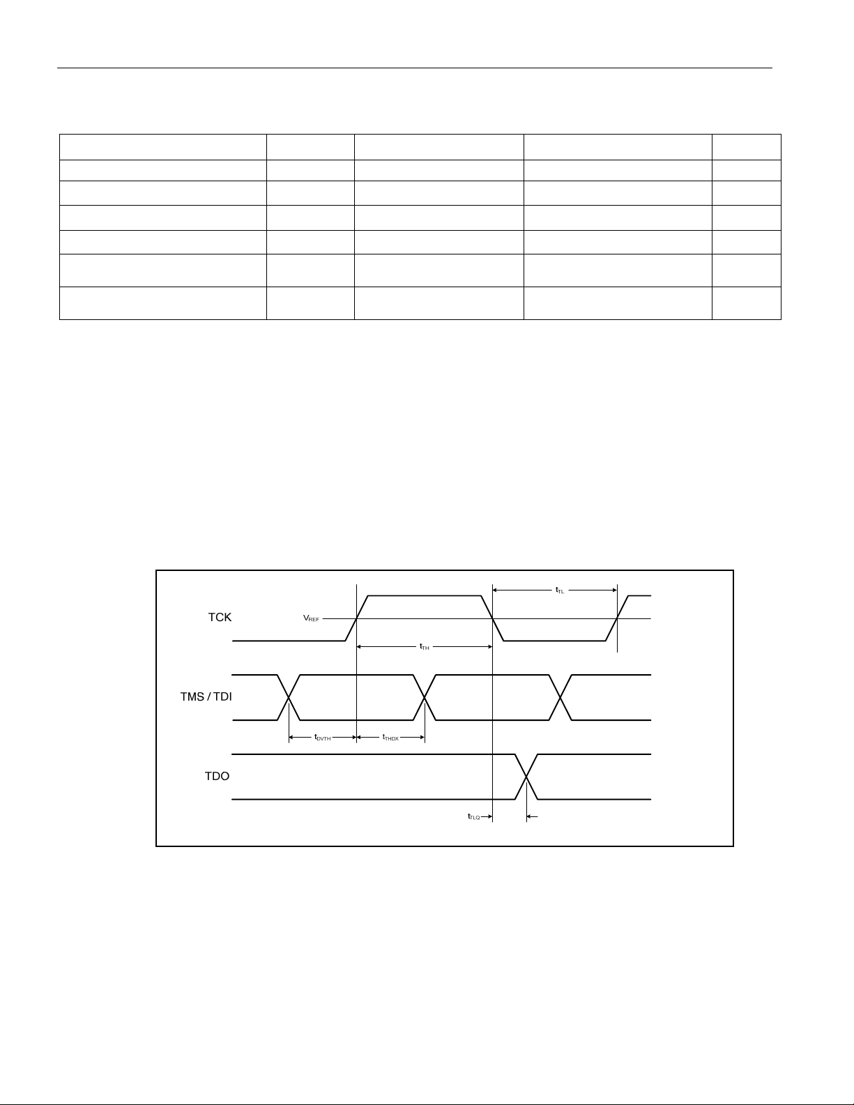
ELECTRICAL CHARACTERISTICS: JTAG INTERFACE
(VDD = 2.5V to 10V, TA = -20°C to +70°C, unless otherwise noted. Typical values are at TA = +25°C, VDD = 5.0V.)
(See Figure 1.)
JTAG Logic Reference V
TCK High Time tTH 4.0 µs
TCK Low Time tTL 4.0 µs
PARAMETER SYMBOL CONDITIONS MIN TYP MAX UNITS
(Note 1) VB ÷ 2 V
REF
TCK Low to TDO Output t
TMS, TDI Input Setup to TCK
High
TMS, TDI Input Hold after TCK
High
1.0 µs
TLQ
1.0 µs
t
DVTH
t
4.0 µs
THDX
Note 1: All voltages referenced to V
Note 2: Internal voltage regulator remains active in SLEEP mode. RAM and registers are powered to maintain contents. RXD and
Note 3: Internal voltage regulator and suspend timer are active in SUSPEND mode. RAM and registers are powered to maintain
Note 4: Internal voltage regulator and ADC are active in ANALOG mode. RAM and registers are powered to maintain contents. ADC data
Note 5: MAXQ core fetches and executes instructions in CPU mode.
Note 6: Parameters guaranteed by design.
Note 7: Voltage A/D readings saturate at 4.85V.
Note 8: f
Note 9: The filter on RXD suppresses noise spikes at the input buffers and delays the sampling instant.
Note 10: V
internal interrupts can be armed by firmware.
contents.
is collected and updated to registers including current accumulation to ACR register.
= 48 × f
OSCA
and VBO will never overlap.
RESET
SAMPLE
.
.
SS
Figure 1. JTAG Timing Diagram
4 of 40

PIN DESCRIPTION
PIN NAME FUNCTION
1, 7–10,
21, 25,
26, 28
2 VIN2
3 VIN1
4 Vx
5 TXD Serial Interface Data Transmit. Maximum of 19200bps.
6 RXD Serial Interface Data Recieve. Maximum of 19200bps.
11 P0.0
12 P0.1
13 SNS2
14 IS2
15 IS1
16 SNS1
17 AVSS
18 VSS
19 P0.2
20 P0.3
22 P0.4 Programmable I/O Pin. Alternate function: [JTAG TDO]
23 P0.5
24 VB
27 VDD
— PAD
N.C.
DS2792 Programmable Fuel Gauge with UART Interface
No Connection
Battery Voltage Sense Input 2. Voltage measurement on VIN2 is
relative to VIN1.
Battery Voltage Sense Input 1. Voltage measurement on VIN1 is
relative to AV
SS
.
Auxiliary ADC Input. Voltage measured ratiometrically with respect
to V
pin voltage or absolutely with respect to internal reference.
B
Programmable I/O Pin. Alternate functions: external interrupt input
INT0, [JTAG TDI].
Programmable I/O Pin. Alternate functions: external interrupt input
INT1, [JTAG TMS].
Current-Sense Input. SNS2 attaches to the pack end of current-
sense resistor.
Current Filter Input 2
Current Filter Input 1
Current-Sense Input. SNS1 attaches to the battery end of current-
sense resistor and V
Analog Supply Return Node. AV
SS
.
attaches to negative battery
SS
terminal.
Digital Supply Return Node. V
attaches to negative battery
SS
terminal.
Programmable I/O Pin. Alternate functions: reset input pin RST.
Programmable I/O Pin. Alternate functions: timer/counter input pin
TCK, [JTAG TCK].
Programmable I/O Pin
Bias Supply Output. Internally regulated to 3.3V. Bypass V
to V
B
SS
with 0.1µF.
Input Supply. +2.5V to +10.0V input range. Bypass V
to VSS with
DD
0.1μF.
Exposed PAD. Not electrically connected to IC. Connect to V
SS
or
leave floating.
5 of 40
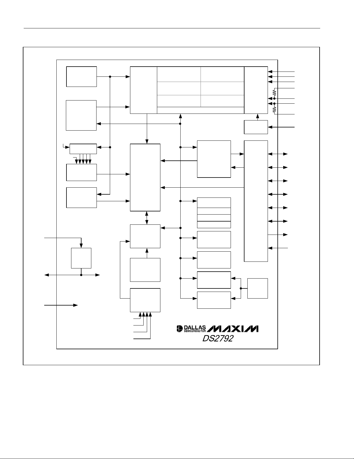
FUNCTIONAL DIAGRAM
DS2792 Programmable Fuel Gauge with UART Interface
PRECISION
ANALOG
OSCILLATOR
SUSPEND
TIMER
TTCK0:1
CLK DIV
P0.3
TIMER/
COUNTER
WATCHDOG
TIMER
VDD
LDO
Regulator
VB VDD_INT
VSS
VSS_INT
TCI
WDI
A/D
CONTROL
BOI, VI,
CI, TI
INTERRUPT
CONTROLLER
MAXQ20
16-BIT RISC
CORE
INSTRUCTION
OSCILLATOR
(1MHz)
JTAG
BOOTLOAD
AND DEBUG
INTERFACE
VOLTAGE1
(VIN1 - AVSS)
VOLTAGE2
(VIN2 - VIN1)
AUX VOLTAGE
(VX - AVSS)
SCI,
SDI
INT0,
INT1
CURRENT
(IS1 - IS2)
AVG CURRENT
TEMPERATURE
ANALOG REGISTERS
UART
INTERFACE
AND
BOOTLOADER
REGISTER FILE
DP[0]
DP[1]
BP[Offs]
256 X 16 SRAM
(DATA)
4K X 16 ROM
(UTILITY)
4K X 16
EEPROM
(PROGRAM)
64 X 16
EEPROM
(DATA)
Tx
Rx
ANALOG
FRONT
END
ADC / MUX
VREF
PORT
PIN
DRIVERS
EEPROM
CHARGE
PUMP
VIN1
VIN2
VX
SNS1
IS1
IS2
SNS2
AVSS
P0.0/INT0/TDI
P0.1/INT1/TMS
P0.2/RST
P0.3/TCK
P0.4/TDO
P0.5
TXD
RXD
P0.3/TCK
P0.1/TMS
P0.0/TDI
P0.4/TDO
6 of 40
DS2792 Programmable Fuel Gauge with UART Interface
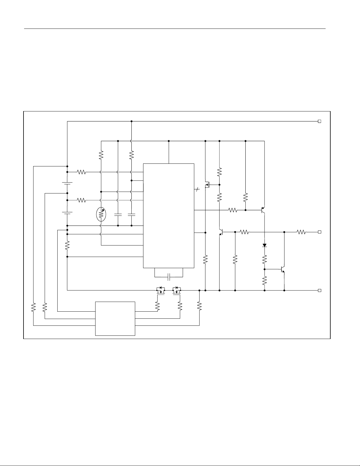
TYPICAL OPERATING CIRCUIT
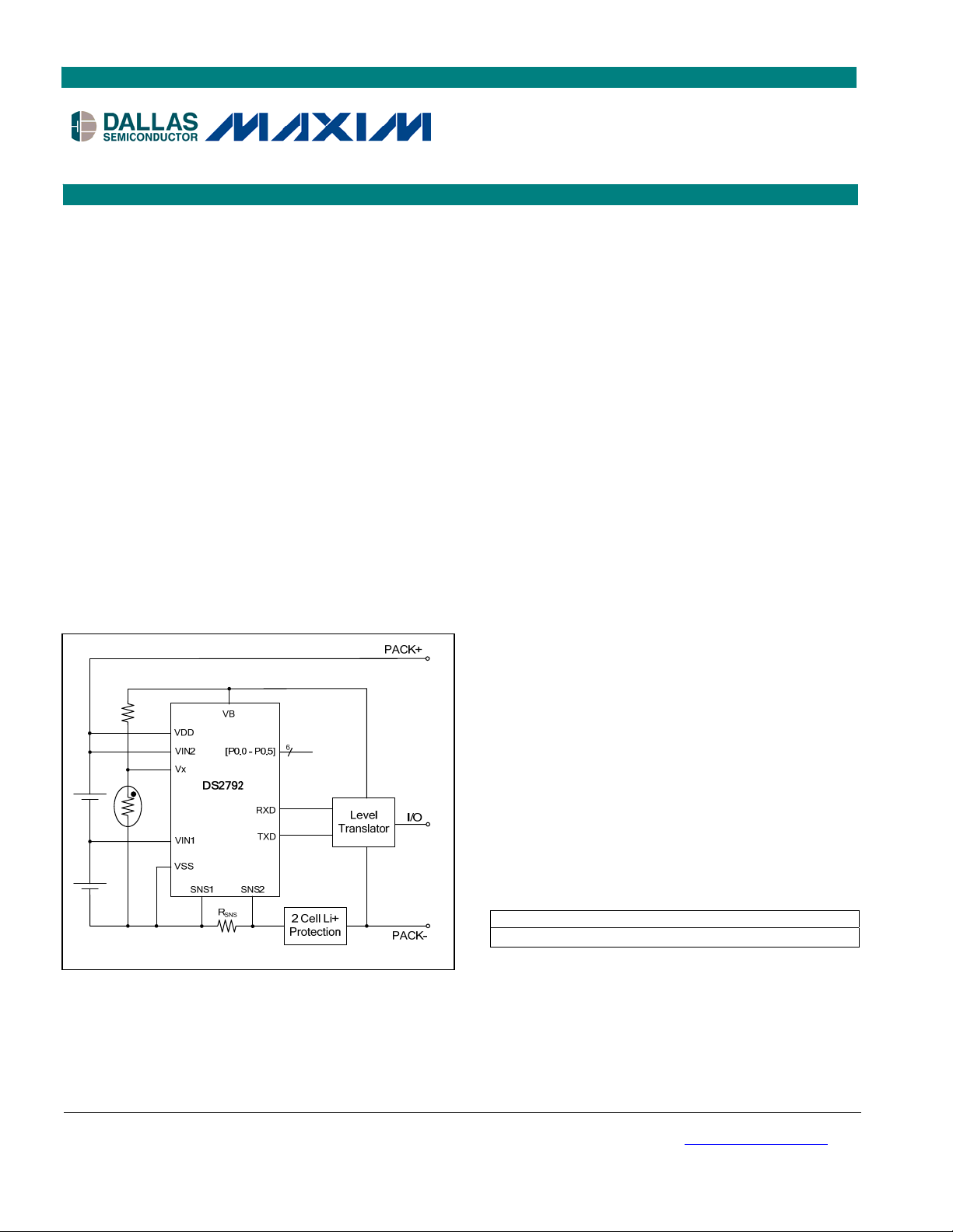
In Figure 2, the DS2792 is connected to the battery side of the pack protector. VDD is isolated with a 150 resistor.
Both V
and the internally regulated voltage VB have 0.1µF bypass capacitors. The VIN1 and VIN2 pins sample
DD
the voltage of each cell. Current flow through the cell pack is monitored by measuring the voltage drop across the
sense resistor R
. Cell temperature is measured ratiometrically through the general-purpose voltage input Vx.
SNS
The GPIO pin P0.5 gates the thermistor circuit to limit current flow between measurements. The UART signals
RXD and TXD are combined into a single 3.3V bidirectional I/O line. The I/O circuit causes no extra current drain
when idle.
Figure 2. Example Pack Circuit with Regulated I/O
PACK+
15010K
1K
1K
AT103-2
VIN2
VDD
Vx
VIN1
0.1µF0.1µF
VB
[P0.0-P0.4]
TxD
BSS84
100
1K
1K
100
2N3906
DS2792
VSS, AVSS
SNS1
R
SNS
P0.5
SNS2
IS1
RxD
IS2
0.1µF
2N2222
1K 1K
100 100
DATA
100
2N2222
1K
PACK-
2-Cell Protection
IC
DETAILED DESCRIPTION
The following is an introduction to the primary features of the DS2792 programmable 2-cell Li-Ion fuel gauge. More
detailed descriptions of the device features can be found in the errata sheets and user's guides described later in
the Additional Documentation section.
DS2792 Overview
The DS2792 incorporates the 16-bit MAXQ20 microcontroller core with 16 accumulators and 16-level hardware
stack. Four memory blocks provide application code space, utility code space, RAM memory, and EEPROM
memory. Specialized peripherals are integrated to perform battery monitoring, coulomb counting, and UART
communication functions. The MAXQ20 core along with the specialized peripherals provide a flexible solution for
fuel gauging of Li-Ion or NiMH battery packs. Flexibility is further enhanced as the solution allows for upgrading of
7 of 40

DS2792 Programmable Fuel Gauge with UART Interface
the program and data EEPROM contents over the UART interface. Updates to the program and data EEPROM are
protected against unauthorized writes by a 256-bit user password. A read protection bit is provided to prevent
reading either EEPROM.
MAXQ20 Core Architecture
The DS2792 employs a MAXQ20 low-cost, high-performance, CMOS, fully static, 16-bit RISC microcontroller with
EEPROM memory. Fetch and execution operations are completed in one cycle without pipelining, since the
instruction contains both the op code and data. The highly efficient core is supported by 16 accumulators and a 16level hardware stack, enabling fast subroutine calling and task switching. Data can be quickly and efficiently
manipulated with three internal data pointers. Multiple data pointers allow more than one function to access data
memory without having to save and restore data pointers each time. The data pointers can automatically increment
or decrement following an operation, eliminating the need for software intervention.
Instruction Set
The instruction set is composed of fixed-length, 16-bit instructions that operate on registers and memory locations.
The instruction set is highly orthogonal, allowing arithmetic and logical operations to use any register along with the
accumulator. Special-function registers control the peripherals and are subdivided into register modules. The family
architecture is modular, so that new devices and modules can reuse code developed for existing products.
The architecture is transport-triggered. This means that writes or reads from certain register locations can also
cause side effects to occur. These side effects form the basis for higher level op codes, such as ADDC, OR, JUMP,
etc. The op codes are implemented as MOVE instructions between register locations, while the assembler handles
the encoding, which need not be a concern to the programmer. The 16-bit instruction word is designed for efficient
execution.
Bit 15 indicates the format for the source field of the instruction. Bits 0 to 7 of the instruction represent the source
for the transfer. Depending on the value of the format field, this can either be an immediate value or a source
register. If this field represents a register, the lower four bits contain the module specifier and the upper four bits
contain the register index in that module.
Bits 8 to 14 represent the destination for the transfer. This value always represents a destination register, with the
lower four bits containing the module specifier and the upper three bits containing the register subindex within that
module. Any time that it is necessary to directly select one of the upper 24 registers as a destination, the prefix
register PFX is needed to supply the extra destination bits. This prefix register write is inserted automatically by the
assembler and requires only one additional execution cycle. Refer to the MAXQ Family User's Guide for complete
instruction set information.
Memory Organization
The DS2792 incorporates several memory areas:
4k Words of utility ROM contain a debugger, program loader, and SHA-1 routines
4k Words of EEPROM memory for application program storage
256 Words of SRAM for storage of temporary variables
64 Words of EEPROM memory for data storage
10 Words of ADC conversion data information
16-level stack memory for storage of program return addresses and general-purpose use
The memory is implemented using the Harvard architecture, with separate address spaces for program and data
memory. A pseudo-Von Neumann memory map is also utilized placing ROM, application code, and data memory
into a single contiguous memory map. The pseudo-Von Neuman memory map allows data memory to be mapped
into program space, permitting code execution from data memory. In addition, program memory can be mapped
into data space, permitting code constants to be accessed as data memory. Figure 3 shows the DS2792’s memory
map when executing from program memory space. Refer to the MAXQ Family User's Guide: DS2792 Supplement
for memory map information when executing from data or ROM space.
8 of 40

DS2792 Programmable Fuel Gauge with UART Interface
The incorporation of EEPROM memory allows field upgrade of the firmware. EEPROM memory can be password
protected with a 16-word key, denying access to program memory by unauthorized individuals. ROM memory is
also available for high-volume, low-cost applications. Contact Dallas Semiconductor for more information on the
availability of ROM-based devices.
Figure 3. DS2792 Memory Map
SYSTEM
REGISTERS
8h
9h
Bh
Ch
Dh
Eh
Fh
00h 0Fh
0h
1h
2h
00h 1Fh
AP
A
PFX
IP
SP
DPC
DP
PERIPHERAL
REGISTERS
M0
M1
M2
16 × 16
STACK
FFFFh
8FFFh
8000h
0FFFh
0000h
PROGRAM
MEMORY SPACE
4K × 16
UTILITY ROM
4K × 16
USER PROGRAM
MEMORY
FFFFh
9FFFh
8000h
027Fh
0200h
01FFh
0000h
DATA MEMORY
(BYTE MODE)
8K × 8
UTILITY ROM
128 × 8
EEPROM DATA
512 × 8
SRAM DATA
FFFFh
8FFFh
8000h
600Ah
6000h
013Fh
0100h
00FFh
0000h
DATA MEMORY
(WORD MODE)
4K × 16
UTILITY ROM
11 × 16
ADC DATA
64 × 16
EEPROM DATA
256 × 16
SRAM DATA
Stack Memory
A 16-bit, 16-level internal stack provides storage for program return addresses and general-purpose use. The stack
is used automatically when the CALL, RET, and RETI instructions are executed and interrupts serviced. The stack
can also be used explicitly to store and retrieve data by using the PUSH, POP, and POPI instructions.
On reset, the stack pointer (SP) initializes to the top of the stack (0Fh). The CALL, PUSH, and interrupt-vectoring
operations increment SP, then store a value at the location pointed to by SP. The RET, RETI, POP, and POPI
operations retrieve the value pointed to by SP, and then decrement SP.
Utility ROM
The utility ROM is a 4k Word block of internal ROM memory that defaults to a starting address of 8000h. The utility
ROM consists of subroutines that can be called from application software. These include:
In-system programming (bootstrap loader) over JTAG or serial interfaces
In-circuit debug routines
Internal self-test routines
Callable routines for in-application EEPROM programming and SHA-1 calculations
Following any reset, execution begins in the utility ROM. The ROM software determines whether the program
execution should immediately jump to location 0000h, the start of application code, or to one of the special routines
9 of 40

DS2792 Programmable Fuel Gauge with UART Interface
mentioned. Routines within the utility ROM are firmware-accessible and can be called as subroutines by the
application software. More information on the utility ROM contents is contained in the MAXQ Family User's Guide:
DS2792 Supplement.
Some applications require protection against unauthorized viewing of program code memory. For these
applications, access to in-system programming, in-application programming, or in-circuit debugging functions is
prohibited until a password has been supplied. The password is defined as the 16 words of physical program
memory at addresses x0010h to x001Fh. Upon startup, code in the ROM examines the password, if a password is
defined (password is other than all zeros or all ones), and the PWL bit remains set, which prohibits access to
commands to read memory contents over the JTAG and serial interfaces.
A single password lock (PWL) bit is implemented in the SC register. When the PWL is set to one (power-on reset
default), the password is required to access the utility ROM, including in-circuit debug and in-system programming
routines that allow reading or writing of internal memory. When PWL is cleared to zero, these utilities are fully
accessible without password. The password is automatically set to all ones following a mass erase.
PROGRAMMING
The EEPROM memory of the microcontroller can be programmed by two different methods: in-system
programming and in-application programming. Both methods afford great flexibility in system design as well as
reduce the life-cycle cost of the embedded system. These features can be password protected to prevent
unauthorized access to code memory.
In-System Programming
An internal bootstrap loader allows the device to be programmed over the JTAG or serial interfaces. As a result,
system software can be upgraded in-system, eliminating the need for a costly hardware retrofit when software
updates are required. Remote software uploads are possible that enable physically inaccessible applications to be
frequently updated. The JTAG interface hardware can be a JTAG connection to another microcontroller, or a
connection to a PC serial port using a serial to JTAG converter such as the MAXQJTAG-001 (3.3V reference
voltage required), available from Maxim Integrated Products. The UART interface hardware can be a connection to
another microcontroller, or a connection to a PC USB port using a USB to UART converter such as the DS9123O,
available from Dallas Semiconductor. A commercial gang programmer can also be used for programming.
Activating the JTAG interface and loading the test access port (TAP) with the system programming instruction
invokes the bootstrap loader for use over the JTAG interface. Setting the SPE bit to 1 during reset through the
JTAG interface executes the bootstrap-loader-mode program that resides in the utility ROM. When programming is
complete and the bootstrap loader exited, the SPE bit will clear and the IC will reset, allowing execution of the
application software.
Performing a program request over the serial interface also invokes the bootstrap loader. The user must
successfully complete a password match (if PWL = 1). The bootstrap loader functions are then fully supported over
the serial interface. When programming is complete, the exit loader function is used to reset the DS2792 and begin
execution of the application software.
The following bootstrap loader functions are supported:
Information commands
Load EEPROM code and data
Dump EEPROM code and data
CRC EEPROM code and data
Verify EEPROM code and data
Erase EEPROM code and data
10 of 40
DS2792 Programmable Fuel Gauge with UART Interface
In-Application Programming
The in-application programming feature allows the microcontroller to modify its own EEPROM program memory.
This allows on-the-fly software updates in mission-critical applications that cannot afford downtime. Alternatively, it
allows the application to develop custom loader software that can operate under the control of the application
software. The utility ROM contains firmware-accessible EEPROM programming functions that erase and program
EEPROM memory. These functions are described in detail in the MAXQ Family User's Guide: DS2792
Supplement.
SYSTEM TIMING
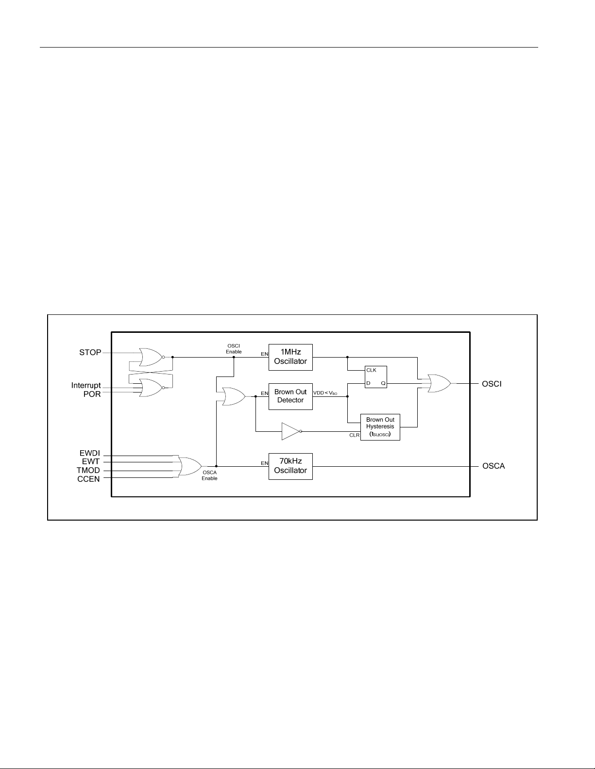
The DS2792 generates its 1MHz instruction clock (OSCI) internally. This quick starting oscillator is used for
instruction fetch and execution by the MAXQ20 core. The analog oscillator (OSCA) is a bandgap-based RC
oscillator that is trimmed to better than 2% accuracy (f
serves as the clock source for the ADC, watchdog timer, and interval timer. OSCA is enabled by the watchdog
timer signals EWDI or EWT, by the timer/counter (TMOD), or by the coulomb counter (CCEN).
OSCI is enabled through either a system interrupt or system POR and disabled through a system stop. A voltage
brownout-detection circuit disables OSCI if V
waits t
OSCI is slaved to OSCA when OSCA is active.
before re-enabling OSCI. To improve overall system timing and meet UART timing requirements,
SU:OSCI
falls below VBO. Once VDD raises above VBO, a hysteresis circuit
DD
ERR:OSCA
Figure 4. System Clocks
). The analog clock runs independent of OSCI and
11 of 40

DS2792 Programmable Fuel Gauge with UART Interface
SYSTEM RESET
Several reset sources are provided for microcontroller control. Although code execution is halted in the reset state,
OSCI continues to run.
Power-On Reset: An internal power-on reset circuit enhances system reliability. This circuit forces the device to
perform a power-on reset whenever a rising voltage on V
climbs above V
DD
. At this point the following events
POR
occur:
All registers and circuits enter their reset state.
The POR flag (WDCN.7) is set to indicate the source of the reset.
Code execution begins at location 8000h.
Watchdog Timer Reset: Software can determine if a reset is caused by a watchdog timeout by checking the
watchdog timer reset flag (WTRF) in the WDCN register. Execution resumes at location 8000h following a
watchdog timer reset.
External System Reset: Asserting the external RST (port P0.2) pin low causes the device to enter the reset state.
The external reset function is described in the MAXQ Family User's Guide. Execution resumes at location 8000h
after the RST pin is released.
MAXQ20 CORE POWER MANAGEMENT
The DS2792 is designed for low-power battery-monitoring applications. The peripherals have been designed with
the ability to wake the processor from SLEEP or ANALOG mode any time software intervention is needed. Power
management is optimized in the applications by performing any necessary processing as quickly as possible, and
re-entering the low power SLEEP or ANALOG mode. Processing resumes from SLEEP or ANALOG mode via any
of the following sources (when enabled):
An external interrupt is triggered.
An external reset signal is applied to the RST pin.
A watchdog timer interrupt occurs.
An internal interrupt event occurs.
Note: No division of the internal system clock is supported, subsequently the PMME and CD[1:0] bits described in
the MAXQ Family User’s Guide are not implemented in the DS2792.
WATCHDOG TIMER
The watchdog timer provides a mechanism to reset the processor in the case of undesirable code execution. The
watchdog timer is a hardware timer designed to be periodically reset by the application software. If the software
operates correctly, the timer is reset before it reaches its maximum count. However, if undesireable code execution
prevents a reset of the watchdog timer, the timer reaches its maximum count and resets the processor.
The watchdog timer in the DS2792 differs in two respects from the one described in the MAXQ Family User's
Guide: 1) the clock used by the timer is the 70kHz OSCA clock that runs independently of the 1MHz OSCI (or
system) clock, and 2) the watchdog interrupt is an asynchronous interrupt that can bring the processor out of stop
mode.
The watchdog timer is controlled through bits in the WDCN register. Its timeout period can be set to one of the four
programmable intervals ranging from 2
occurs at the end of this timeout period, which is 512 OSCA clock periods, or 7.3ms, before the reset.
12
to 221 OSCA clock periods (59ms up to 30s). The watchdog interrupt
12 of 40

DS2792 Programmable Fuel Gauge with UART Interface
DS2792 POWER MODES
When power is first applied to the DS2792, a power-on-reset (POR) circuit transitions the IC to brownout state
where cell voltage is monitored. If V
and begins code execution. Firmware determines if the IC switches to ANALOG mode or low-power SLEEP mode
when a STOP halts CPU operation.
The DS2792 enters SLEEP mode after a CPU STOP if the ADC and all internal timers are disabled and the
suspend timer is off. In SLEEP mode, all IC operation becomes inactive except for external activity interrupts.
Brownout detection does not occur in SLEEP mode. Any interrupt generated by UART communication or external
input on ports P0.0 or P0.1 will transition the DS2792 from SLEEP to brownout to verify cell voltage before
returning to CPU mode. If the suspend timer is enabled, the IC will transition from SLEEP to ANALOG mode if a
suspend timeout occurs.
The DS2792 enters ANALOG mode after a CPU STOP if any one of the following is active: the ADC, the interval
timer, or the watchdog timer. An external interrupt or an interrupt from any active internal circuit causes the DS2792
to transition back to CPU mode to service the condition.
If the DS2792 is in ANALOG or CPU mode, and V
enters the brownout state. In brownout state, the processor is halted without changing the instruction pointer. If V
voltage rises above V
within a time of t
BO
interrupt (if enabled). Otherwise, if V
waits to receive an interrupt.
Note that the supply rise time at initial power up of the IC must be faster than t
entering SLEEP mode prior to software enabling external interrupts. If this situation occurs, the DS2792 remains in
SLEEP until power cycled.
Figure 5. DS2792 State Diagram
voltage is above the brownout threshold VBO, the DS2792 enters CPU mode
DD
falls below VBO, a brownout condition occurs and the DS2792
DD
, the DS2792 returns to CPU mode and generates a brown-out
SU:OSCI
remains below V
DD
BO
for t
, the DS2792 again enters SLEEP mode and
SU:OSCI
to prevent the DS2792 from
SU:OSCI
Power On Reset
DD
Brown-Out
VDD < V
BO
Brown-Out Recovery
VDD > VBO for t
SU:OSCI
CPU Disabled.
B
r
o
T
i
t
>
w
m
n
e
t
S
U
:
External
Interrupt
u
t
-
O
t
o
u
I
S
C
O
Brown-Out
External Interrupts
Monitored
ADC Active
Interrupt
CPU STOP
Analog Circuits Active
VDD < V
Code Execution
BO
CPU STOP
Analog Circuits Inactive
Suspend Timeout
Suspend Timer Enabled
13 of 40

DS2792 Programmable Fuel Gauge with UART Interface
SUSPEND TIMER
The suspend timer allows the DS2792 to periodically monitor the cell while spending the majority of its time in a
low-power state. Suspend operation is managed through the coulomb counter control register (CCCON). A timout
value between 0.5s and 2.0s can be selected through the suspend timeout bits (CCSUS). When the suspend timer
is enabled and a timeout occurs, the DS2792 will transition from SLEEP mode to ANALOG mode, and eventually to
CPU mode. Upon transition to ANALOG mode, the coulomb counter enable bit (CCEN) is automatically set and the
ADC block becomes active. The DS2792 may then perform all needed cell-monitoring operations before clearing
the CCEN bit and returned to SLEEP mode. The process repeats after each timeout.
Figure 6. CCCON Register Format
FIELD BIT FORMAT ALLOWABLE VALUES
Reserved
CCSUS 2:1 R/W Suspend Timeout
CCEN 0 R/W Coulomb Counter Enable
7:3 Read Only Undefined
0 0 = Suspend Timeout Disabled
0 1 = 0.5s timeout
1 0 = 1.0s timeout
1 1 = 2.0s timeout
0 = ADC block disabled
1 = ADC block enabled
REGISTER SET
Most functions of the device are controlled by sets of registers. These registers provide a working space for
memory operations as well as configuring and addressing peripheral registers on the device. Registers are divided
into two major types: system registers and peripheral registers. The common register set, also known as the
system registers, includes the ALU, accumulator registers, data pointers, interrupt vectors and control, and stack
pointer. The peripheral registers define additional functionality that may be included by different products based on
the MAXQ20 architecture. This functionality is broken up into discrete modules so that only the features required
for a given product need to be included. Tables 1 through 6 detail the DS2792 register set.
Table 1. System Register Map
MODULE NAME (BASE SPECIFIER) REGISTER
INDEX
00h AP
01h APC
02h —
03h —
04h PSF
05h IC
06h IMR
07h —
08h SC
09h —
0Ah —
0Bh
0Ch —
0Dh —
0Eh CKCN
0Fh WDCN
Note: Names that appear in italics indicate that all bits of a register are read-only. Names that appear in bold indicate that a register is 16 bits
wide. Registers in module AP are bit addressable.
AP (8h) A (9h) PFX (Bh) IP (Ch) SP (Dh) DPC (Eh) DP (Fh)
IIR
A[0] PFX IP
A[1]
A[2]
A[3]
A[4]
A[5]
A[6]
A[7]
A[8]
A[9]
A[10]
A[11]
A[12]
A[13]
A[14]
A[15]
— —
— —
— — — Offs
— — —
— — —
— —
— —
— — — GRS —
— — — GRH —
— — — GRXL —
— — FP —
—
— — — — —
— — — — —
— — — — —
— — — — —
— — —
SP
IV
LC0
LC1 BP DP1
—
—
—
—
DP0
DPC
GR
GRL —
—
—
14 of 40

Table 2. System Register Bit Functions
REGISTER
AP
APC
PSF
IC
IMR
SC
IIR
CKCN
WDCN
A[n] (0..15)
PFX
IP
SP
IV
LC[0]
LC[1]
Offs
DPC
GR
GRL
BP
GRS
GRH
GRXL
FP
DP[0]
DP[1]
15 14 13 12 11 10 9 8 7 6 5 4 3 2 1 0
— — — — AP (4 bits)
CLR IDS — — — MOD2 MOD1 MOD0
Z S — GPF1 GPF0 OV C E
— — CGDS — — — INS IGE
IMS — —
TAP — —
IIS — —
—
POR EWDI
— — — — — — — — — — — — SP (4 bits)
Offs (8 bits)
— — — — — — — — — — — WBS2 WBS1 WBS0 SDPS1 SDPS0
GR.15 GR.14 GR.13 GR.12 GR.11 GR.10 GR.9 GR.8 GR.7 GR.6 GR.5 GR.4 GR.3 GR.2 GR.1 GR.0
GRL.7 GRL.6 GRL.5 GRL.4 GRL.3 GRL.2 GRL.1 GRL.0
GRS.15 GRS.14 GRS.13 GRS.12 GRS.11 GRS.10 GRS.9 GRS.8 GRS.7 GRS.6 GRS.5 GRS.4 GRS.3 GRS.2 GRS.1 GRS.0
GRH.7 GRH.6 GRH.5 GRH.4 GRH.3 GRH.2 GRH.1 GRH.0
GRXL.15 GRXL.14 GRXL.13 GRXL.12 GRXL.11 GRXL.10 GRXL.9 GRXL.8 GRXL.7 GRXL.6 GRXL.5 GRXL.4 GRXL.3 GRXL.2 GRXL.1 GRXL.0
DS2792 Programmable Fuel Gauge with UART Interface
REGISTER BIT NUMBER
A[n] (16 bits)
PFX (16 bits)
IP (16 bits)
IV (16 bits)
LC[0] (16 bits)
LC[1] (16 bits)
BP (16 bits)
FP (16 bits)
DP[0] (16 bits)
DP[1] (16 bits)
— — —
— —
— — —
— — — — — — —
— —
WDIF WTRF EWT RWT
IM1 IM0
ROD PWL —
II1 II0
15 of 40

DS2792 Programmable Fuel Gauge with UART Interface
Table 3. System Register Bit Reset Values
REGISTER
AP 0 0 0 0 0 0 0 0
APC 0 0 0 0 0 0 0 0
PSF 1 0 0 0 0 0 0 0
IC 0 0 0 0 0 0 0 0
IMR 0 0 0 0 0 0 0 0
SC 0 0 0 0 0 0 s 0
IIR 0 0 0 0 0 0 0 0
CKCN 0 s s 0 0 0 0 0
WDCN s s 0 0 0 0 0 0
A[n] (0..15) 0 0 0 0 0 0 0 0 0 0 0 0 0 0 0 0
PFX 0 0 0 0 0 0 0 0 0 0 0 0 0 0 0 0
IP 1 0 0 0 0 0 0 0 0 0 0 0 0 0 0 0
SP 0 0 0 0 0 0 0 0 0 0 0 0 1 1 1 1
IV 0 0 0 0 0 0 0 0 0 0 0 0 0 0 0 0
LC[0] 0 0 0 0 0 0 0 0 0 0 0 0 0 0 0 0
LC[1] 0 0 0 0 0 0 0 0 0 0 0 0 0 0 0 0
Offs 0 0 0 0 0 0 0 0
DPC 0 0 0 0 0 0 0 0 0 0 0 1 1 1 0 0
GR 0 0 0 0 0 0 0 0 0 0 0 0 0 0 0 0
GRL 0 0 0 0 0 0 0 0
BP 0 0 0 0 0 0 0 0 0 0 0 0 0 0 0 0
GRS 0 0 0 0 0 0 0 0 0 0 0 0 0 0 0 0
GRH 0 0 0 0 0 0 0 0
GRXL 0 0 0 0 0 0 0 0 0 0 0 0 0 0 0 0
FP 0 0 0 0 0 0 0 0 0 0 0 0 0 0 0 0
DP0 0 0 0 0 0 0 0 0 0 0 0 0 0 0 0 0
DP1 0 0 0 0 0 0 0 0 0 0 0 0 0 0 0 0
Note: s indicates bit reflects pin state.
15 14 13 12 11 10 9 8 7 6 5 4 3 2 1 0
REGISTER BIT
16 of 40

DS2792 Programmable Fuel Gauge with UART Interface
Table 4. Peripheral Register Map
REGISTER
INDEX
00h PO
01h PPU
02h PAF — — 12h — — —
03h
04h
05h
06h
07h TCC — — 17h — — —
08h
09h — — — 19h
0Ah — SADEN — 1Ah
0Bh — SADDR — 1Bh ICDF — —
0Ch —
0Dh — — ECNTL 1Dh ICDA — —
0Eh — —
0Fh — —
Note: Names that appear in italics indicate that all bits of a register are read-only. Names that appear in bold indicate that a register is 16 bits.
All locations are bit addressable.
M0 (0h) M1 (1h) M2 (2h)
EIC SMD
EINT
CCCON
TC PR
PI
MODULE MODULE
SINT
SMASK
SBUF — 14h — — —
SCON — 15h — — —
— — 18h
BRE
— 10h — — —
— 11h — — —
— 13h — — —
— 16h — — —
— 1Ch ICDB — —
EADDR
EDATA
REGISTER
INDEX
1Eh ICDD — —
1Fh — — —
M0 (0h) M1 (1h) M2 (2h)
ICDT0
ICDT1
ICDC
— —
— —
— —
17 of 40

Table 5. Peripheral Register Bit Functions
REGISTER
PO
PPU
PAF
EIC
EINT
CCCON
TC
TTC
PI
ICDT0
ICDT1
ICDC
ICDF
ICDB
ICDA
ICDD
SINT
SMASK
SMD
SBUF
SCON
PR
SADEN
SADDR
BRE
Note: Names that appear in italics indicate a read-only register bit.
15 14 13 12 11 10 9 8 7 6 5 4 3 2 1 0
— — PO.5 PO.4 PO .3 PO.2 PO.1 PO .0
TxD_PU RxD_PU PPU.5 PPU.4 PPU.3 PPU.2 PPU.1 PPU.0
— RSTD PAF.5 PAF.4 PAF.3 PAF. 2 PAF.1 PAF.0
MBOI MSCI MSDI
BOI SCI SDI
THI.7 THI.6 THI.5 THI.4 THI.3 THI.2 THI.1 THI.0 TLOW.7 TLOW.6 TLOW.5 TLOW.4 TLOW.3 TLOW.2 TLOW.1 TLOW.0
— — — — — TTCK.1 TTCK.0 TMOD
—
ICDT0.15 ICDT0.14 ICDT0.13 ICDT0.12 ICDT0.11 ICDT0.10 ICDT0.9 ICDT0.8 ICDT0.7 ICDT0.6 ICDT0.5 ICDT0.4 ICDT0.3 ICDT0.2 ICDT0.1 ICDT0.0
ICDT1.15 ICDT1.14 ICDT1.13 ICDT1.12 ICDT1.11 ICDT1.10 ICDT1.9 ICDT1.8 ICDT1.7 ICDT1.6 ICDT1.5 ICDT1.4 ICDT1.3 ICDT1.2 ICDT1.1 ICDT1.0
— — — — PSS.1 PSS.0 SPE TXC
ICDB.7 ICDB.6 ICDB.5 ICDB. 4 ICDB.3 ICDB.2 ICDB.1 ICDB.0
ICDA.15 ICDA.14 ICDA.13 ICDA.12 ICDA.11 ICDA.10 ICDA.9 ICDA.8 ICDA.7 ICDA.6 ICDA.5 ICDA.4 ICDA.3 ICDA.2 ICDA.1 ICDA.0
ICDD.15 ICDD.14 ICDD.13 ICDD.12 ICDD.11 ICDD.10 ICDD.9 ICDD.8 ICDD.7 ICDD.6 ICDD.5 ICDD.4 ICDD.3 ICDD.2 ICDD.1 ICDD.0
— — — — — — TINT RINT
— — — — — — MTI MRI
— — TXDi RXDi — — SMOD FEDE
SBUF.7 SBUF.6 SBUF.5 SBUF.4 SBUF.3 SBUF.2 SBUF.1 SBUF.0
FE/SM0 SM1 SM2 REN T B8 RB8 TI RI
PR.15 PR.14 PR.13 PR.12 PR.11 PR.10 PR.9 PR.8 PR.7 PR.6 PR.5 PR.4 PR.3 PR.2 PR.1 PR.0
SAME.7 SAME.6 SAME.5 SAME.4 SAME.3 SAME. 2 SAME.1 SAME.0
SAD.7 SAD.6 SAD.5 SAD.4 SAD.3 SAD.2 SAD.1 SAD.0
BRE.15 BRE.14 BRE.13 BRE.12 BRE.11 BRE.10 BRE.9 BRE.8 BRE.7 BRE.6 BRE.5 BRE.4 BRE.3 BRE.2 BRE.1 BRE.0
—
— — MVI MCI MTI MTCI PIP.1 PIP.0 PIT.1 PIT.0 PIE.1 PIE.0
—
— — VI CI TI TCI — — —
DS2792 Programmable Fuel Gauge with UART Interface
REGISTER BIT NUMBER
INT.1 INT.0
RST
— — — — — CCSUS.1 CCSUS.0 CCEN
RxDI PI.5 PI.4 PI.3 PI.2 PI.1 PI.0
DME — REGE — CMD.3 CMD.2 CMD.1 CMD.0
18 of 40

DS2792 Programmable Fuel Gauge with UART Interface
Table 6. Peripheral Register Reset Values
REGISTER
PO
PPU
PAF
EIC
EINT
CCCON
TC
TTC
PI
ICDT0
ICDT1
ICDC
ICDF
ICDB
ICDA
ICDD
SINT
SMASK
SMD
SBUF
SCON
PR
SADEN
SADDR
BRE
Note: s indicates bit reflects pin state.
15 14 13 12 11 10 9 8 7 6 5 4 3 2 1 0
0 0 1 1 1 1 1 1
0 0 0 0 0 1 0 0
0 0 0 0 0 1 0 0
0 0 0 0 0 0 0 0 0 0 0 0 0 0 0 0
0 0 0 0 0 0 0 0 0 0 0 0 0 0 0 0
0 0 0 0 0 0 0 0
0 0 0 0 0 0 0 0 0 0 0 0 0 0 0 0
0 0 0 0 0 0 0 0
s s s s s s s s
0 0 0 0 0 0 0 0 0 0 0 0 0 0 0 0
0 0 0 0 0 0 0 0 0 0 0 0 0 0 0 0
0 0 0 0 0 0 0 0
0 0 0 0 0 0 0 0
0 0 0 0 0 0 0 0
0 0 0 0 0 0 0 0 0 0 0 0 0 0 0 0
0 0 0 0 0 0 0 0 0 0 0 0 0 0 0 0
0 0 0 0 0 0 0 0
0 0 0 0 0 0 0 0
0 0 0 0 0 0 0 0
0 0 0 0 0 0 0 0
0 0 0 0 0 0 0 0
0 0 0 0 0 0 0 0 0 0 0 0 0 0 0 0
0 0 0 0 0 0 0 0
0 0 0 0 0 0 0 0
0 0 0 0 0 0 0 0 0 0 0 0 0 0 0 0
REGISTER BIT NUMBER
ON-CHIP REGULATOR
The DS2792 provides a regulated 3.3V output on the VB pin capable of supplying up to 2mA of current to external
circuitry. The regulated supply can be used to level shift the I/O lines and/or provide a reference voltage for the Vx
pin to measure a pack ID resistor or thermistor. The regulator output is always active regardless of the DS2792’s
mode of operation.
SYSTEM INTERRUPTS
Multiple interrupt sources are available for quick response to internal and external events. The MAXQ20
architecture uses a single interrupt vector (IV), single interrupt-service routine (ISR) design. For maximum flexibility,
interrupts can be enabled globally, individually, or by module. When an interrupt condition occurs, its individual flag
is set, even if the interrupt source is disabled at the local, module, or global level. Interrupt flags must be cleared
within the firmware-interrupt routine to avoid repeated interrupts from the same source. Application software must
ensure a delay between the write to the flag and the RETI instruction to allow time for the interrupt hardware to
remove the internal interrupt condition. Asynchronous interrupt flags require a one-instruction delay and
synchronous interrupt flags require a two-instruction delay.
When an enabled interrupt is detected, execution jumps to a user-programmable interrupt vector location. The IV
register defaults to 0000h on reset or power-up, so if it is not changed to a different address, application firmware
must determine whether a jump to 0000h came from a reset or interrupt source.
Once control has been transferred to the ISR, the interrupt identification register (IIR) can be used to determine if a
system register or peripheral register was the source of the interrupt. The specified module can then be
interrogated for the specific interrupt source and software can take appropriate action. Interrupts are evaluated by
application code allowing the definition of a unique interrupt priority scheme for each application. Interrupt sources
are available from the watchdog timer described in the MAXQ Users Guide, the SINT register described in the
UART Interrupts section, and the EINT register as shown in Figure 7.
19 of 40

DS2792 Programmable Fuel Gauge with UART Interface
EINT Register
The EINT register contains interrupts generated by the ADC, the timer counter, the general-purpose port pins, and
the UART RXD pin. Their masks and their configuration bits, along with the RST pin status and control, are present
in the EIC and PAF registers of module 0.
Figure 7. EINT Register Interrupt Sources
GENERATOR INTERRUPT MASK DESCRIPTION FREQUENCY
Ports and Pins
INT0 PAF.0/PIE.0
INT1 PAF.1/PIE.1
SCI MSCI
SDI MSDI
The interrupt from pin P0.0 is configurable
via the PAF.0, PIT.0, and PIP.0 bits.
The interrupt from pin P0.1 is configurable
via the PAF.1, PIT.1, and PIP.1 bits.
The serial connect interrupt is generated
when RXD becomes high.
The serial disconnect interrupt is generated
when RXD is low for at least 220ms.
Dependent on external
conditions.
Dependent on external
conditions.
Rising edge on RXD.
Once every 220ms if RXD
is held low. The first
interrupt may take up to
440ms from the time RXD
goes low. Interrupt will not
trigger if the ADC is off.
Brownout
Detector
A/D Converter
Timer/
Counter
BOI MBOI
VI MVI
CI MCI
TI MTI
TCI MTCI
The brownout interrupt indicates that V
was below V
the microcontroller's stop mode. It will interrupt
the microcontroller, if MBOI is 1, after a
charger brings V
microcontroller to run.
The voltage interrupt indicates the voltage
registers in the data peripheral memory block
have fresh voltage averages.
The current interrupt indicates that the
current register (6004h) in the data peripheral
memory block has a fresh reading and that the
ACR has also been updated.
The temperature interrupt indicates that the
temperature register in the data peripheral
memory block has a fresh average.
The timer/counter interrupt indicates that the
timer/counter has been reloaded after reaching
its end-count.
in the past. It will not terminate
BO
above VBO and causes the
DD
DD
Every time after exiting
brownout.
Once every 13.8ms.
Never if the ADC is off.
Once every 88ms. Never if
the ADC is off.
Once every 220ms. Never
if the ADC is off.
Dependent on TMOD and
TTCK[1:0].
20 of 40

DS2792 Programmable Fuel Gauge with UART Interface
I/O PORTS
The DS2792 includes a simple input/output (I/O) data port. From a software perspective, the port appears as a
group of special-function registers within module M0. The simple I/O port defined for this product is described
below:
CMOS input buffers
Four open-drain output drivers with selectable tri-state or weak pullups
Two selectable open-drain or push-pull output drivers with selectable tri-state
Support alternate functions and TAP controller interface signals
Two pins have interrupt capability
The port is accessed through five peripheral registers (PO, PI, PAF, PPU, and EIC) addressed either by byte or by
individual bit locations. The I/O port is designed to provide programming flexibility for the application. All individual
I/O pins are independently configured; and can be defined as an input, output, or alternate function. Table 7
summarizes the functionality of the I/O pins.
Table 7. I/O Port Pins
FUNCTIONS CHARACTERISTICS
Primary Alternate TAP* Bidirectional
P0.0 INT0 TDI* Configurable, [In] — Configurable, [Off] —
P0.1 INT1 TMS* Configurable, [In] — Configurable, [Off] —
P0.2
RST* —
Configurable, [In] — Configurable, [Off] —
P0.3 — TCK* Configurable, [In] — Configurable, [Off] —
P0.4 — TDO* Configurable, [In] — — Configurable, [Off]
P0.5 — — Configurable, [In] — — Configurable, [Off]
TXD — — Output Configurable, [On] Configurable, [Off] —
RXD — — Input Configurable, [On] Configurable, [Off] —
Note: Reset values are denoted with an * and by [ ].
PI Register: The PI register is a read-only input of the I/O pins. When the register is read, the logic level of each
pin is reported in the corresponding bit locations. Reading a logic-low or high on a pin does not change the output
drive on that pin.
PO Register: The PO register controls the output state of the I/O pins. Data written to this register determines the
pin output drive. When a bit is written to a “0” (cleared), the n-channel output drive transistor is enabled, and the
pullup is disabled. When bit is written to a “1” (set), the n-channel output drive transistor is disabled, and the pullup
enabled (if so configured). The PO bits are set asynchronously during power-on reset to disable the N-channel
output drive. PO bits are not altered in SLEEP mode, however drive to the n-channel is disabled.
PPU Register: The PPU register contains independent bits that define each pin as high impedance or pulled up
when its n-channel output drive transistor is disabled. P0.0 through P0.3 have weak pullups, P0.4 and P0.5 have
strong pullups. When the output is disabled and the PPU bit is cleared, the pin is high impedance. When the output
is disabled and the PPU bit is set, the pin’s weak or strong pullup is enabled. When the PPU bit is set and the
device enters STOP mode, the weak pullup remains enabled.
PAF Register: The PAF register enables or disables the alternate functions of P0.0–P0.2. When a pin’s PAF bit is
cleared, the pin is controlled by the PI, PO, PPU, and EIC registers. When the PAF bit is set, the pin operates in it’s
alternate function mode. The RST function of P0.2 can be disabled by writing the RSTD bit to 1.
EIC Register: The lower six bits of the EIC register are the port interrupt control bits. The port interrupt control bits
are used to enable and configure detection of external interrupts. Interrupt enable bits, PIE.0 and PIE.1, enable
detection of an interrupt on pins P0.0 and P0.1, respectively. Interrupt type bits, PIT.0 and PIT.1, define the type
(level or edge) of interrupt on pins P0.0 and P0.1, respectively. Interrupt polarity bits, PIP.0 and PIP.1, determine
the interrupt polarity on pins P0.0 and P0.1, respectively.
Weak Passive
Pulldown
Weak Active Pullup Strong Active Pullup
21 of 40

DS2792 Programmable Fuel Gauge with UART Interface
Table 8. P0 Interrupt Configuration
PIE.x PIT.x PIP.x RESULT
0 X X Interrupt Disabled
1 0 0 Interrupt Enabled, Triggered on Logic-Low
1 0 1 Interrupt Enabled, Triggered on Logic-High
1 1 0 Interrupt Enabled, Triggered on Falling Edge
1 1 1 Interrupt Enabled, Triggered on Rising Edge
Figure 8. Port Pin Schematics
22 of 40

DS2792 Programmable Fuel Gauge with UART Interface
PROGRAMMABLE TIMER/COUNTER
The timer/counter block operates as a simple 8-bit interval timer or counter. The start value is programmable and is
automatically reloaded when a rollover occurs. The TMOD bit in the TCC register selects between the counter and
timer modes. In the counter mode, external events on the P0.3 pin are counted. In the timer mode, OSCA clock
source cycles are counted. The OSCA clock and brownout detectors continue to run if the CPU is stopped.
Figure 9. Timer/Counter Block Diagram
The timer low byte (TLOW) is used to count input events, while the timer high byte (THI) is used to store the reload
value. Firmware must initialize TLOW and THI with the same value for the first count to be the same as succeeding
counts. TLOW counts up until FFh is reached, it is then automatically reloaded with the value in THI. THI remains
unchanged unless modified by firmware. The clock source is selected with TTCK[1:0] bits. Table 9 describes the
possible resolution and range of the timer.
Table 9. Programmable Timer Configuration
TMOD TTCK[1:0] CLOCK PERIOD TIMER RANGE (t x 28)
1 0 0 14.3µs 3.66ms
1 0 1 343µs 87.9ms
1 1 0 6.86ms 1.76s
1 1 1 220ms 56.3s
0 N/A Counter Mode
23 of 40

DS2792 Programmable Fuel Gauge with UART Interface
SERIAL INTERFACE MODULE
The DS2792 supports a universal asynchronous receiver/transmitter (UART) module for serial communication with
framing error detection and automatic address recognition. The UART is initialized through a configuration register
(SMD). Communication is managed through a control register (SCON) and a transmit/receive register (SBUF). The
SBUF register location provides access to both transmit and receive registers, where a read is directed to the
receive buffer and a write is directed to the transmit buffer. SBUF allows the serial interface to receive an incoming
word before software has read the previous one provided SBUF is read before the stop bit of the next word is
recieved.
If the DS2792 detects a start bit of an incoming transmission while in SLEEP mode, the instruction clock will be
enabled to allow reception of data. Note that the instruction clock will not achieve accuracy tolerance required for
UART communication unless the analog oscillator is also active. All outgoing transmission must be completed, and
the RXD pin must be in the inactive logic state (see RXDi bit), before the DS2792 will transition back to SLEEP
mode.
Figure 10. Serial Interface Control Register (SCON)
FIELD BIT FORMAT ALLOWABLE VALUES
Serial Interface Mode Bit 0/Framing Error Flag
The operation of this bit depends on the state of the FEDE bit
of the SMD register. When FEDE is cleared to 0, this bit
functions as SM0 and controls the operating mode. See Serial
FE/SM0 7 R/W
SM1 6 R/W
SM2 5 R/W
REN 4 R/W
TB8 3 R/W
RB8 2 R/W
TI 1 R/W
RI 0 R/W
Interface Modes, Table 10.
When FEDE is set to 1, this bit functions as a framing error flag
and will automatically be set to 1 when the incoming stop bit
has been received as a logic 0. When used as FE, this flag
must be cleared to 0 by software.
Serial Interface Mode Bit 1
See Serial Interface Modes, Table 10
Serial Interface Mode Bit 2
Mode 1 operation:
0 = Normal operation
1 = RXI flag not set if incoming stop is logic 0
Modes 2 and 3 operation:
0 = Multiprocessor mode disabled
1 = Multiprocessor mode enabled
Reciever Enable
0 = Reciever enabled
1 = Reciever disabled
Transmit Data Bit 8
When in mode 2 or 3, this bit determines the state of the ninth
transmitted data bit. This bit is not used in mode 1.
Received Data Bit 8
When in mode 2 or 3, this bit indicates the state of the incoming
ninth data bit. In mode 1, this bit indicates the state of the stop
bit.
Transmit Interrupt Flag
Set to 1 at the end of the last data bit transmitted.
TI must be cleared by software.
Recieve Interrupt Flag
Set to 1 at the end of the stop bit sampling window when in
mode 1. Set to 1 at the end of the sampling window of the ninth
data bit when in mode 2 or 3.
RI must be cleared by software.
24 of 40

DS2792 Programmable Fuel Gauge with UART Interface
Figure 11. Serial Interface Configuration Register (SMD)
FIELD BIT FORMAT ALLOWABLE VALUES
Reserved
7:6 Read Only
Undefined
TXD Invert Bit
TXDi 6 R/W
0 = Normal operation
1 = TXD output signal inverted
RXD Invert Bit
RXDi 5 R/W
0 = Normal operation
1 = RXD input data inverted
Reserved
3:2 Read Only
Undefined
Baud Rate Doubler
SMOD 1 R/W
0 = Baud rate divided by 2 (mode 2)
0 = Baud rate divided by 4 (modes 1 and 3)
1 = Baud rate unchanged
Framing Error Enable Flag
FEDE 0 R/W
0 = SICON bit 7 controls communication mode (SM0)
1 = SICON bit 7 flags framing errors (FE)
Figure 12. Serial Interface Block Diagram
SBUF Output Shift Register
RI
TI
Modes 2&3 only
D7
Stop
D8
D0
Start
Bit
Latch
TXD
BAUD Clock
÷16
TB8
SBUF Input Register
RB8
D8 (Modes 2&3)
Stop bit (Mode 1)
D8
Stop
Modes 2&3 only
Input Shift Register
D7
D7
D0
D0
Start
REN
Start Detect
Bit
Detect
RXD
25 of 40

DS2792 Programmable Fuel Gauge with UART Interface
Serial Interface Modes of Operation
The UART operates in one of three asynchronous full-duplex communication modes with different protocols and
baud rates. Two mode bits (SM1, SM0 in the SCON register) are used to select the modes of operation. The
operating modes are summarized in Table 10.
Table 10. Serial Interface Modes
SM1 SM0 MODE FUNCTION CLOCK LENGTH START/STOP
0 1 1
1 0 2
1 1 3
Mode 1
Mode 1 is asynchronous, full duplex with a 10-bit data stream consisting of a logic 0 start bit, eight data bits, and
logic 1 stop bit. The data is transferred least significant bit first. The UART begins transmission several cycles after
the first baud clock of the baud rate generator following a write to SBUF. Transmission on the TXD pin begins with
the start bit, data then is shifted out on the pin, least significant bit first, followed by the stop bit. The TI bit is set two
clock cycles after the stop bit is transmitted. All bits are shifted out at the rate determined by the baud rate
generator. Baud rate generation is discussed in the Baud Rate Generation section.
Once the baud rate generator is active, reception can begin at any time. The REN bit in SCON must be set to logic
1 to enable the reception. The falling edge of a start bit on the RXD pin will begin the reception process. Data will
be shifted in at the selected baud rate. At the middle of the stop bit time slot, certain conditions must be met to load
SBUF with the received data from the receive shift register:
RI must be 0, and
if SM2 is 0, the state of the stop bit does not matter, or
if SM2 is 1, the state of the stop bit must be 1
If these conditions are true, the SBUF register will be loaded with the received byte, the RB8 bit will be loaded with
the stop bits and the RI bit will be set. If these conditions are false, then SBUF and RB8 will not be loaded, the
received data will be lost and the RI bit will not be set. Regardless of the receive word status, the receive logic will
go back to looking for a 1 to 0 transition on the RXD pin after the middle of the stop bit time.
Each data bit received is sampled on the 7th, 8th, and 9th clock from the baud rate generator (running 16 times
faster than communication speed). Using majority voting, two equal samples out of the three determine the logic
value for each received bit. If the start bit was determined to be invalid, then the receive logic returns to looking for
a 1 to 0 transition on the RXD pin in order to start the reception again.
Asynchronous
Full Duplex
Asynchronous
Full Duplex
Asynchronous
Full Duplex
Phase Delta
Register
Instruction Clock 9 1 Start, 1 Stop TB8, RB8
Phase Delta
Register
8 1 Start, 1 Stop N/A
9 1 Start, 1 Stop TB8, RB8
9th BIT
FUNCTION
26 of 40

DS2792 Programmable Fuel Gauge with UART Interface
Figure 13. Timing Diagram for Serial Interface Mode 1
Mode 2
Mode 2 is asynchronous, full-duplex communication with an 11-bit data stream consisting of a logic 0 start bit, eight
data bits, a programmable 9th bit, and a logic 1 stop bit. The data is transferred least significant bit first. Similar to
mode 1, transmissions occur on the TXD pin and reception on the RXD pin. For transmission purposes, the 9th bit
can be configured as logic 0 or 1. A common use is to load this location with a parity bit. The 9th bit is transferred
from the TB8 bit position in the SCON register during the write to SBUF. The UART will begin transmission a few
cycles after the first rollover of the clock source divided by 16 following a write to SBUF. Transmission begins with
the start bit being placed on the TXD pin, data is then shifted onto the pin, least significant bit first, followed by the
9th bit, and finally the stop bit. The TI bit is set at the same time the stop bit is transmitted on the TXD pin. All bits
are shifted out at the rate determined by the baud rate generator. Baud rate generation is discussed in the Baud
Rate Generation section.
Once the baud rate generator is active, reception can begin at any time. The REN bit must be set to a logic 1 to
enable the reception. The falling edge of a start bit on the RXD pin will begin the reception process. Data will be
shifted in at the selected baud rate. At the middle point of the 9th bit time slot, certain condition must be met to load
SBUF with the received data from the receive shift register:
RI must be 0, and
if SM2 is 0, the state of the stop bit does not matter, or
if SM2 is 1, the state of the 9th bit must be 1
27 of 40

DS2792 Programmable Fuel Gauge with UART Interface
If these conditions are true, then SBUF will be loaded with the received byte, the RB8 bit will be loaded with the 9th
bit, and the RI bit will be set. If these conditions are false, then SBUF and RB8 will not be loaded, the received data
will be lost, and RI bit will not be set. Regardless of the receive word status, the receive logic will go back to looking
for a 1 to 0 transition on the RXD pin after the middle point of the stop bit time slot.
Each data bit received is sampled on the 7th, 8th, and 9th clock from the baud rate generator (running 16 times
faster than communication speed). Using majority voting, two equal samples out of the three determine the logic
value for each received bit. If the start bit was determined to be invalid, then the receive logic goes back to looking
for a 1 to 0 transition on the RXD pin in order to start the reception again.
Mode 3
Operation of mode 3 is identical to mode 2 except for the baud rate source. Baud rate generation is discussed in
the Baud Rate Generation section.
Figure 14. Timing Diagram for Serial Interface Modes 2 and 3
Transmit Frequency
Serial Interface Clock So urce divided by 16
Start
7th, 8th, and 9th Samples
Start
D1D0 D8 Stop
of each bit
D1D0 D8 Stop
D2 D3 D4 D5 D6 D7
D2 D3 D4 D5 D6 D7
Transmit Frequency
Serial Interface Clock So urce divided by 16
Detection of Framing Errors
A framing error occurs during communication when a valid stop bit is not detected. The result is a possible
improper reception of the serial word. The serial inteface will notify the system by setting the framing error (FE) bit
in the SCON register to 1. When set, the FE bit must be cleared by software or a system reset. Receiving a
properly framed serial word will not clear the FE bit.
28 of 40

DS2792 Programmable Fuel Gauge with UART Interface
Note that both the FE and the serial mode bit 0 (SM0) share the same bit location in the SCON register, but this
information is actually stored in different registers. The setting of FEDE in the SMD register determines which
register is accessed: logic 0 allows access to the SM0 bit and a logic 1 allows access to the FE bit. The FEDE must
be set to 1 while reading or writing the FE bit.
Multiprocessor Communication Mode
Multiprocessor communication mode makes special use of the 9th data bit in modes 2 and 3 if the SM2 bit of the
SCON register is set. If enabled, the 9th data bit is used to signify that the incoming byte is an address. This allows
the processor to be interrupted only if the correct address is received as defined by the serial address (SADDR)
and serial address enable (SADEN) registers. The receive interrupt, if enabled, will only occur when a recognized
address is received.
When multiprocessor mode is enabled and a serial word is received with the 9th bit set, the byte will be assumed to
be an address. The address will be compared to an internally stored address. If it matches, a receive interrupt will
occur. The internal address is derived from the SADDR and SADEN registers. The SADDR register specifies an
absolute address. This is the user specified address of the device. The SADEN register indicates which address
bit(s) will be used in the comparison. This allows broadcast transmissions that reach multiple microcontrollers or all
microcontrollers on the serial interface. The user defines this protocol.
Software will write an 8-bit address to the SADDR register. This is the microcontroller’s individual address. Any bit
in SADEN that contains logic 0 will cause the corresponding bit in SADDR to be ignored in comparison. Thus, logic
0 bits in SADEN create don’t care bit states for address comparisons. When an address is received, each address
bit that is not masked by a don’t care will be compared to the SADDR. The microcontroller will interrupt on any
address that matches this comparison. Any address that meets this comparison is called a given address. The
following example shows how one address can be directed to an individual processor or two out of three.
Micro 1 Micro 2 Micro 3
SADDR 11110000 SADDR 11110001 SADDR 11110010
SADEN 11111010 SADEN 11111001 SADEN 11111010
––––––––––––––– ––––––––––––––– –––––––––––––––
Given 11110x0x Given 11110xx1 Given 11110x1x
Note that an address of 11110000 reaches only microcontroller 1. An address of 11110001 reaches microcontroller
1 and microcontroller 2. An address of 11110010 reaches only microcontroller 3. The microcontroller also matches
on any address that corresponds to the broadcast address. This is the logical OR of the SADDR and SADEN
registers, with any 0s defined as don’t cares.
UART Interrupts
Interrupts generated by the serial interface are controlled through the serial interface interrupt register (SINT) and
the serial interface interrupt mask register (SMASK). Writing either the receive interrupt mask (MRI) bit or transmit
interrupt mask (MTI) bit to 1 will enable interrupts to occur whenever the corresponding transaction successfully
completes. Writing either of these bits to 0 disables the corresponding interrupt. The RINT, TINT bits of the SMASK
are a logical AND of the RI flag, TI flag bits of the control register, and the corresponding interrupt mask bits.
Upon successful reception of a data word on RXD, the RI flag of the SCON register will be set. If MRI is set to 1,
the RINT flag will be set and an interrupt will be generated. System software can then read the SINT register to
determine the source of the interrupt. The RINT flag and the interrupt are cleared by writing the RI flag to 0. After
transmission of a data word on TXD, the TI flag of the SCON register will be set. If MTI is set to 1, the TINT flag will
be set and an interrupt will be generated. System software can then read the SINT register to determine the source
of the interrupt. The TINT flag and the interrupt are cleared by writing the TI flag to 0.
29 of 40

DS2792 Programmable Fuel Gauge with UART Interface
Command Codes
The DS2792 has two reserved command codes: a software power-on reset (POR) of the IC and an instruction to
begin program loading over the serial interface. Each command code is enabled by transmitting a <break>, 0xFE,
<break>, followed directly by the command instruction. There are no associated data bytes with either command.
Any other serial communication between the instructions negates the operation. See the MAXQ Family User's
Guide: DS2792 Supplement for the serial interface programming procedure. These command codes are fixed
inside the DS2792 and cannot be altered. System firmware should avoid using FEh as a command code during
device operation. A <break> instruction is defined as holding the RXD line low until a framing error is generated.
Table 11. Serial Interface Command Codes
COMMAND HEX CODE PURPOSE
Command Enable <break>, FEh, <break> Enable soft POR or program command.
Soft POR FEh Causes a reset of the IC.
Request Programming FDh Initiates programming over the serial interface.
Available
00h–FCh, FFh Defined by application firmware.
Baud Rate Generation
The baud rate for serial communication is derived directly from the instruction oscillator OSCI. The method for baud
rate generation depends on the serial interface’s operating mode. In operating modes 1 and 3, the baud rate is
determined by the value stored in the phase delta (PR) register. In operating mode 2, the OSCI oscillator sets the
baud rate directly. The baud rate doubler (SMOD) bit in the SMD register can be used to double the baud rate in
mode 2 or quadruple the baud rate in modes 1 and 3. Note that the baud clock frequency generated by this circuit
will be the sampling frequency used by the serial interface and is therefore 16 times the actual communication rate.
Figure 15. Baud Rate Generation Circuit
In mode 2, baud rates are generated directly from the system clock. The baud rate for mode 2 is given by the
formula: Baud Rate = (2
the system clock frequency. In the above formula, the numerator is expressed as two to the power of SMOD,
where SMOD is either a 0 or 1. The SMOD bit effectively doubles the baud rate when set to logic 1. The SMOD bit
is set to logic 0 on reset, which gives the lower speed baud rate.
SMOD
÷ 32) × f
. The result of this formula generates a baud rate of either 1/16 or 1/32 of
OSCI
30 of 40

DS2792 Programmable Fuel Gauge with UART Interface
In modes 1 and 3, the baud rate generator creates a phase accumulator that generates a baud clock as the result
of phase overflow into the most significant bit of the phase shift circuitry. As shown in Figure 15, a 16-bit phase
delta register (PR) is used to select a suitable phase delta for its baud clock. The phase delta is used to provide a
predetermined phase increment to the phase accumulator. The phase accumulator is formed by a 17-bit register
and a 16-bit adder. When the baud rate generator is enabled, the content of the phase delta register adds to the
value of the 17-bit register triggered by the system clock, essentially performing a phase accumulation. The baud
clock is the result of the adder carry output to the most significant bit of the 17-bit register. The baud rate for modes
1 and 3 are given by the formula: baud rate = (PR × f
) ÷ 223 × 2
OSCI
(SMOD×2)
. The SMOD bit effectively quadruples
the baud rate when set to logic 1. The SMOD bit is set to logic 0 on reset, which gives the lower speed baud rate.
Table 12. Sample Baud Rate Settings
MODE SMOD
PR REGISTER
BAUD RATE
2 0 N/A 30583 baud
2 1 N/A 61166 baud
1 or 3 1 1416h 2400 baud
1 or 3 1 282Dh 4800 baud
1 or 3 1 505Bh 9600 baud
1 or 3 1 A0B7h 19200 baud
1 or 3 0 282Dh 1200 baud
Baud rate calculations are based on a system clock frequency of 978.656KHz. Note that the analog oscillator must
be active for reliable serial communication. If OSCA is inactive, the OSCI timebase error f
ERR:OSCI
may be greater
than the UART communication standard of 3%.
Baud Rate Error Adjustment
The baud rate error (BRE) register provides error information that can be used by software to correct small errors in
the DS2792’s baud rate compared to the transmitting IC’s baud rate by adjusting the value loaded in the phase
delta register. At the end of each data word successfully received, the BRE register is updated with a 0.125%
resolution two’s complement value representing the percent difference between the expected final logic transition
on TXD compared to the final logic transition as measured by the bit sampler. A positive error means the UART is
running too slow and a negative error means the UART is running too fast.
Figure 16. Baud Rate Error Register Format
S 2
14
213 212 211 210 29 28 27 26 25 24 23 22 21 2
0
MSb LSb
“S”: sign bit(s)
For example: Communication is occurring at 9600 baud (PR register contains 505Bh) in mode 1, and a value of
C5h is received by the UART. The final RXD transition between bit D7 (logic 0) and the stop bit (logic 1) is
expected to occur between sample 16 of the 7th bit and sample 1 of the 8th bit. After transmission is complete, the
BRE register is found to contain a value of 08h indicating the final logic transition occurred 1.0% early. The master
is transmitting data at a rate of roughly 1.0% faster than the DS2792’s present baud rate. The PR register is
updated to a value of 5129h (101% of 505Bh) to correct the transmission rate difference. It is recommended that
the PR register is adjusted by only a fraction of the calculated error amount after each byte to prevent oscillation of
the frequency setting.
Note that for dynamic baud rate error adjustment to be successful, the starting frequency difference must be within
±½ bit period at the final logic transition point (±50% if the final transition is between start and D0, ±25% if the final
transition is between D0 and D1, etc). The BRE register is read only and is cleared on reset.
Units: 20 = 0.125%
31 of 40

DS2792 Programmable Fuel Gauge with UART Interface
ANALOG-TO-DIGITAL CONVERSION
The DS2792 performs real-time measurements of system temperature, voltage, current, and accumulated current.
The DS2792’s ADC is controlled by an internal state machine that sequences the measurements, and stores the
results in memory. The conversion results of the ADC are mapped into data memory starting at word address
6000h, as shown in Table 13.
The DS2792 current measurement system is designed to provide timely data on charge and discharge current at a
moderate resolution level while simultaneously accumulating high resolution average data to support accurate
coulomb counting. Current is measured by sampling the voltage drop across a series sense resistor, R
connected between SNS1 and SNS2. Individual current samples are taken every 1/f
(687µs). All samples are
SAMPLE
averaged to report current, average current, and accumulated current values.
The DS2792 measures voltage on three separate inputs. The voltage of the lower cell, VIN1, is reported as the
measured difference between the VIN1 pin and analog ground pin AV
. The voltage of the upper cell, VIN2, is
SS
reported as the difference between the VIN2 and VIN1 pins. The auxiliary voltage, Vx, is reported both as an
absolute value of the difference between the Vx pin and AVSS, and as a ratio metric percentage of the voltage of
the V
pin. Individual voltage samples are taken approximately every 5/f
B
(3.43ms). Multiple samples are
SAMPLE
averaged to update the voltage measurement registers.
The DS2792 measures temperature directly on chip. Individual temperature samples are taken every 10/f
(6.87ms). Multiple samples are averaged to update the average temperature register.
Table 13. ADC Related Registers
WORD
ADDRESS
6000h Read Only Vx Voltage Ratiometric
6001h Read Only Vx Voltage Absolute
6002h Read Only VIN2 Voltage
6003h Read Only VIN1 Voltage
6004h Read Only Current
6005h Read Only Temperature
6006h R/W Accumulated Current
6007h Read Only Accumulated Current (Middle Word)
6008h Read Only Accumulated Current (Lower Word)
6009h Read Only Average Current
600Ah R/W ADC Configuration
ACCESS DESCRIPTION
Current Measurement
The voltage signal developed across the sense resistor (between SNS1 and SNS2) is differentially sampled by the
ADC inputs via internal 10k resistors connected between SNS1 and IS1, and SNS2 and IS2. Isolating the ADC
inputs (IS1 and IS2 pins) from the sense resistor with 10k facilitates the use of an RC filter by adding a single
external capacitor. The RC filter extends the effective input range beyond ±64mV in pulse load or pulse charge
applications. The ADC accurately measures large peak signals as long as the differential signal level at IS1 and
IS2 does not exceed ±64mV.
The current register reports the average of 128 individual current samples every 88ms. The reported value
represents the average current during the 88ms measurement period. Figure 17 specifies the update interval and
resolution of the current register. Values are posted in two’s complement format. Positive values represent charge
currents (V
IS1
> V
) and negative values represent discharge currents (V
IS2
IS2
> V
). Positive currents above the
IS1
maximum register value are reported at the maximum value, 7FFFh. Negative currents below the minimum register
value are reported at the minimum value, 8000h.
SNS
SAMPLE
,
32 of 40

DS2792 Programmable Fuel Gauge with UART Interface
Figure 17. Current Register Format
12-bit + sign resolution (13-bit), 88ms update interval
Word Address 6004h
11
S 2
210 29 28 27 26 25 24 23 22 21 20 X X X
MSb LSb
“S”: sign bit(s)
CURRENT RESOLUTION (1 LSB)
R
|V
SS
- V
SNS
|
25m 20m 15m 10m
SNS
15.625µV 625µA 781µA 1.042mA 1.56mA
CURRENT INPUT RANGE
R
V
- V
SNS
25m 20m 15m 10m
SS
SNS
±64mV ±2.56A ±3.2A ±4.27A ±6.40A
Units: 20 = 15.625μV/R
SNS
The average current register reports the average of 4096 current samples over a 2.8s measurement period. Figure
18 specifies the update interval and resolution of the average current register. Values are posted in the same
format as the current register, but with an additional 3 bits of resolution. Positive currents above the maximum
register value are reported at the maximum value, 7FFFh. Negative currents below the minimum register value are
reported at the minimum value, 8000h.
Figure 18. Average Current Register Format
15-bit + sign resolution (16-bit), 2.8s update interval
Word Address 6009h
S 2
14
213 212 211 210 29 28 27 26 25 24 23 22 21 2
0
MSb LSb
“S”: sign bit(s)
AVERAGE CURRENT RESOLUTION (1 LSB)
R
|V
SS
- V
SNS
|
25m 20m 15m 10m
SNS
1.953µV 78.13µA 97.66µA 130.2µA 195.3µA
Units: 2
0
= 1.953μV/R
SNS
Automatic Current Offset Correction
Continuous offset cancellation is performed automatically to correct for offsets in the current measurement system.
Individual values reported by the current register have a maximum offset of ±0.5 bits (±7.8125µV). Individual values
reported in the average current register have a maximum offset of ±4 bits (±7.8125µV).
33 of 40

DS2792 Programmable Fuel Gauge with UART Interface
Current Measurement Bias
Systematic errors or an application preference can require the application of an arbitrary bias to the current
measurement process. The current measurement bias value sets a user-programmed positive or negative bias to
the current measurement. The current measurement bias value can be used to estimate battery currents that do
not flow through the sense resistor, estimate battery self-discharge, or correct for offset error in the current
registers. The user-programmed two’s complement value is added to the current register once per current sample.
The bias control is applied in 0.98μV increments over a ±125μV range. When using a 15mΩ sense resistor, the
bias control can be adjusted in 65.3μA increments over a ±8.33mA range. The current measurement bias bit field is
located in the upper byte of the ADC configuration register.
Figure 19. Current Measurement Bias Field
Upper Byte of Word Address 600Ah
S 26 25 24 23 22 21 20
MSb LSb
“S”: sign bit
Units: 20 = 0.98μV/R
SNS
Current Accumulation
Current measurements are internally accumulated and displayed in the accumulated current register (ACR). The
accuracy of the ACR is dependent on both the current measurement and the accumulation time base. The 16-bit
ACR has a range of ±204.8mVh with a resolution of 6.25µVh. Accumulation of charge current above the maximum
register value is reported at the maximum value; conversely, accumulation of discharge current below the minimum
register value is reported at the minimum value. Read and write access is allowed to the ACR.
Figure 20. Accumulated Current Register Format
Word Address 6006h
S 214 213 212 211 210 29 28 27 26 25 24 23 22 21 2
0
MSb LSb
“S”: sign bit(s)
ACR RESOLUTION (1 LSB)
R
|V
SS
- V
SNS
| / R
SNS
25m 20m 15m 10m
SNS
6.25µVh 0.25mAh 0.312mAh 0.416mAh 0.625mAh
ACR ACCUMULATION RANGE
R
|V
SS
- V
SNS
| / R
SNS
25m 20m 15m 10m
SNS
±204.8mVh ±8.192Ah ±10.24Ah ±13.65Ah ±20.48Ah
Units: 2
0
= 6.25μVh/R
SNS
34 of 40

DS2792 Programmable Fuel Gauge with UART Interface
-1
The lower 32 bits of ACR resolution (bits 2
6008h respectively. Note that since the lower bits are from separate address words it cannot be guaranteed that
they will contain data from the same measurement as the main ACR register at the time of reading. However, two
consecutive reads from addresses 6006h–6008h that contain the same data ensures that all data is from the same
measurement. When the ACR register is written, the lower ACR bits are automatically cleared.
to 2
-32
) can be read by firmware from address locations 6007h and
Accumulation Blanking
In order to avoid the accumulation of small positive offset errors over long periods, an offset blanking filter is
provided. The blanking filter is enabled by setting the OBEN bit in the ADC configuration register. When OBEN is
set, charge currents (positive values from the current register) less than 62.5μV are not accumulated in the ACR.
The minimum charge current accumulated in the ACR is 4.167mA for R
= 0.015Ω.
SNS
Voltage Measurements
The DS2792 continually measures the voltage between pins VIN1 and AVSS and between pins VIN2 and VIN1 over
a 0.0V to V
with a resolution of 4.88mV. Voltages above the maximum register value are reported as the maximum value.
range. The VIN1 and VIN2 voltage registers are updated in two’s complement format every 13.8ms
FS
Figure 21. VIN1 Voltage Register Format
Word Address 6003h
S 29 28 27 26 25 24 23 22 21 20 X X X X X
MSb LSb
“S”: sign bit Units: 20 = 4.88 mV
Figure 22. VIN2 Voltage Register Format
Word Address 6002h
S 29 28 27 26 25 24 23 22 21 20 X X X X X
MSb LSb
“S”: sign bit Units: 20 = 4.88 mV
The DS2792 continually measures the voltage between pins Vx and VSS. The result is reported in two’s
complement absolute and ratiometric formats every 20ms. The Vx ratiometric voltage result is a ratio of voltage on
the Vx pin relative to the voltage on the V
the internal reference and has a resolution of 4.88mV. Voltages above the maximum register value are reported as
the maximum register value.
Figure 23. Vx Ratiometric Register Format
pin. The LSb weighting is VB/1024. The Vx absolute voltage result uses
B
Word Address 6000h
S 2
9
28 27 26 25 24 23 22 21 20 X X X X X
MSb LSb
“S”: sign bit Units: 20 = VB/1024
35 of 40

DS2792 Programmable Fuel Gauge with UART Interface
Figure 24. Vx Absolute Voltage Register Format
Word Address 6001h
9
S 2
28 27 26 25 24 23 22 21 20 X X X X X
MSb LSb
“S”: sign bit Units: 20 = 4.88 mV
Temperature Measurement
The DS2792 uses an integrated temperature sensor to continually measure battery temperature. Temperature
measurements are updated in the temperature register every 220ms in two’s complement format with a resolution
of 0.125°C over a ±127°C range. The temperature register format is shown in Figure 25.
Figure 25. Temperature Register Format
Word Address 6005h
S 29 28 27 26 25 24 23 22 21 20 X X X X X
MSb LSb
“S”: sign bit
Units: 2
0
= 0.125°C
ADC Configuration Register
The ADC configuration register located at word address 600Ah controls current measurement bias and offset
blanking. ADC configuration register bits are read and write accessable by application code. IBIAS bits are
described in the current measurement bias section above. Offset blanking is controlled by the OBEN bit. If offset
blanking is enabled, the DS2792 assumes small positive currents do not occur in the application. Small positive
readings are considered A/D measurement error and are not accumulated.
Figure 26. ADC Configuration Register Format
ADDRESS 600Ah BIT DEFINITION
Field Bit Format Allowable Values
Current Measurement Bias
IBIAS 15:8 R/W
Reserved
OBEN 0 R/W
7:1 Read Only
8-bit two’s complement value that is added to the current
measurement on every update.
Undefined
Offset Blanking Enable
0 = All current measurements are accumulated into the ACR.
1 = Positive current measurements less than 62.5µV/R
accumulated into the ACR.
are not
SNS
PASSWORD-PROTECTED USER TRIM
System software can change current measurement gain, power-up state of the UART, and undervoltage threshold
of the IC through the user trim in program EEPROM (word addresses 001Eh–001Fh). The user trim values are
enabled through the trim key in the lower byte of address 001Fh. If the trim key is set to 76h, the user-trim values
replace the default trim values, if the trim key is set to any other value, default trim is selected. Note that either all
user-trim values are enabled or none are enabled. Figure 27 shows the format of all values that can be adjusted
and their default trim values.
36 of 40

DS2792 Programmable Fuel Gauge with UART Interface
Figure 27. User Trim Registers
ADDRESS 001Eh BIT DEFINITION
Field Bit Format Allowable Values
Current Gain Trim
These bits adjust the current gain by ±25%. The most significant
bit is the two’s complement sign bit, 1 LSB = 0.195%.
IG 15:8 R/W
SRTC 7:0 R/W
ADDRESS 001Fh BIT DEFINITION
Field Bit Format Allowable Values
BD9600 15 R/W
TXDi 14 R/W
RXDi 13 R/W
UVT 12:8 R/W
Trim Key 7:0 R/W
Example: A4h (-92d) adjusts the trim by -17.94%.
Valid only if trim key = 76h
Default = factory trim value
Sense Resistor Temperature Coefficient
These bits adjust the current gain based on temperature of the
sense resistor. 1 LSB = 30.5ppm/ºC.
Example: 1Ah (26d) adjusts current measurements for a sense
resistor with a 793ppm/ºC temperature coefficient.
Valid only if trim key = 76h
Default = 00h
Force UART BAUD Rate at Power-On Reset
0 = 19200 BAUD
1 = 9600 BAUD
Valid only if trim key = 76h
Default = 0
TXDi Bit Power-On Reset Value
0 = Normal Operation
1 = TXD Output Signal Inverted
Valid only if trim key = 76h
Default = 0
RXDi Bit Power-On Reset Value
0 = Normal Operation
1 = RXD Input Data Inverted
Valid only if trim key = 76h
Default = 0
Undervoltage Threshold
The undervoltage threshold ranges from 4.60V to 5.80V and is
calculated by the equation:
V
= 5.80V - 0.039V × UVT[4:0]
UV
Valid only if trim key = 76h
Default = 17h (2.45V)
Trim Key
Enables or disables all other user-trim values.
76h = all user trim values valid
Other = all user trim values invalid (default trim used)
37 of 40

DS2792 Programmable Fuel Gauge with UART Interface
IN-CIRCUIT DEBUG
Embedded debugging capability is available through the JTAG-compatible test access port. Embedded debug
hardware and embedded ROM firmware provide in-circuit debugging capability to the user application, eliminating
the need for an expensive in-circuit emulator. Figure 28 shows a block diagram of the in-circuit debugger. The incircuit debug features include:
A hardware debug engine.
A set of registers able to set breakpoints on register, code, or data accesses (ICDA, ICDB, ICDC, ICDD, ICDF,
ICDT0, and ICDT1).
A set of debug service routines stored in the utility ROM.
Figure 28. In-Circuit Debugger
The embedded hardware debug engine is an independent hardware block in the microcontroller. The debug engine
can monitor internal activities and interact with selected internal registers while the CPU is executing user code.
Collectively, the hardware and software features allow two basic modes of in-circuit debugging:
Background mode allows the host to configure and set up the in-circuit debugger while the CPU continues to
execute the application software at full speed. Debug mode can be invoked from background mode.
Debug mode allows the debug engine to take control of the CPU, providing read/write access to internal
registers and memory, and single-step trace operation.
38 of 40

DS2792 Programmable Fuel Gauge with UART Interface
APPLICATIONS
The low-power, high-performance RISC architecture of the DS2792 makes it an excellent fit for many portable or
battery-powered applications that require cost-effective computing and analog measurement capability. The highthroughput core is programmable in circuit over the UART and JTAG interfaces, allowing for firmware upgrades
and ease of code development. Applications benefit from UART and GPIO peripheral interfaces allowing the
microcontroller to communicate with many external devices. The DS2792’s high level of integration reduces
component count and board space, critical factors in the design of portable systems.
The DS2792 is ideally suited for applications such as fuel gauging, sensor conditioning, and data collection.
ADDITIONAL DOCUMENTATION
Designers must have four documents to fully use all the features of this device. This data sheet contains pin
descriptions, feature overviews, and electrical specifications. Errata sheets contain deviations from published
specifications. The user’s guides offer detailed information about device features and operation. The following
documents can be downloaded from www.maxim-ic.com/DS2792
.
The DS2792 data sheet, which contains electrical/timing specifications and pin descriptions, available at
www.maxim-ic.com/DS2792
The DS2792 errata sheet, available at www.maxim-ic.com/errata.
The MAXQ Family User's Guide, which contains detailed information on core features and operation, including
programming at www.maxim-ic.com/products/MAXQUG
The MAXQ Family User's Guide: DS2792 Supplement, which contains detailed information on features specific
.
.
to the DS2792 at www.maxim-ic.com/DS2792UG.
DEVELOPMENT AND TECHNICAL SUPPORT
A variety of highly versatile, affordably priced development tools for this microcontroller are available from
Maxim/Dallas Semiconductor and third-party suppliers, including:
Compilers
In-circuit emulators
Integrated development environments (IDEs)
Serial-to-JTAG converters for programming and debugging
USB-to-JTAG converters for programming and debugging
Technical support is available through email at batterymanagement.support@dalsemi.com
.
39 of 40

PIN CONFIGURATION
DS2792 Programmable Fuel Gauge with UART Interface
DS2792G+
NC
VIN2
VIN1
Vx
TXD
RXD
NC
NC
NC
NC
TDI/INT0/P0.0
TMS/INT1/P0.1
SNS2
IS2
1
2
3
4
5
6
7
8
9
10
11
12
13
14
PAD
8mm × 4mm TDFN-28
28
NC
27
VDD
26
NC
25
NC
24
VB
23
P0.5
22
P0.4/TDO
21
NC
20
P0.3/TCLK
19
P0.2/RST
18
VSS
17
AVSS
16
SNS1
15
IS1
PACKAGE INFORMATION
(The package drawing(s) in this data sheet may not reflect the most current specifications. For the latest package outline information, go to
www.maxim-ic.com/DallasPackInfo
.)
40 of 40
Maxim/Dallas Semiconductor cannot assume responsibility for use of any circuitry other than circuitry entirely embodied in a Maxim/Dallas Semiconductor product.
No circuit patent licenses are implied. Maxim/Dallas Semiconductor reserves the right to change the circuitry and specifications without notice at any time.
Maxim Integrated Products, 120 San Gabriel D rive, Sunnyvale, CA 94086 408-737-7600
The Maxim logo is a registered trademark of Maxim Integrated Products, Inc. The Dallas logo is a registered trademark of Dallas Semiconductor Corporation.
© 2007 Maxim Integrated Products • Printed USA
 Loading...