

Page 1
General Description
The DS2788 measures voltage, temperature, and current, and estimates available capacity for rechargeable
lithium-ion (Li+) and Li+ polymer batteries. Cell characteristics and application parameters used in the calculations are stored in on-chip EEPROM. The available
capacity registers report a conservative estimate of the
amount of charge that can be removed given the current temperature, discharge rate, stored charge, and
application parameters. Capacity estimation is reported
in mAh remaining and percentage of full.
LED display drivers and a debounced input make display of the capacity information easy. The LED pins can
directly sink current, requiring only a resistor for setting
the current in the LED display, thus reducing space and
cost.
Applications
Power Tools
Electric Bicycles
Electric Vehicles
Uninterruptible Power Supply
Digital Cameras
Features
♦ Five 30mA Open-Drain Drivers for Driving LED
Fuel-Gauge Display
♦ Debounced Fuel-Gauge Display Enable
♦ Internal Voltage Measurement Gain Register for
Trimming External Voltage-Divider
♦ Pin for Driving FETs to Enable Voltage-Divider
Only During Voltage Measurement, Conserving
Power
♦ Precision Voltage, Temperature, and Current
Measurement System
♦ Accurate, Temperature-Stable, Internal Time Base
♦ Absolute and Relative Capacity Estimated from
Coulomb Count, Discharge Rate, Temperature,
and Battery Cell Characteristics
♦ Accurate Warning of Low Battery Conditions
♦ Automatic Backup of Coulomb Count and Age
Estimation to Nonvolatile (NV) EEPROM
♦ Gain and Tempco Calibration Allows the Use of
Low-Cost Sense Resistors
♦ 24-Byte Battery/Application Parameter EEPROM
♦ 16-Byte User EEPROM
♦ Unique ID and Multidrop 1-Wire
®
Interface
♦ 14-Pin TSSOP Package
DS2788
Stand-Alone Fuel-Gauge IC with
LED Display Drivers
________________________________________________________________
Maxim Integrated Products
1
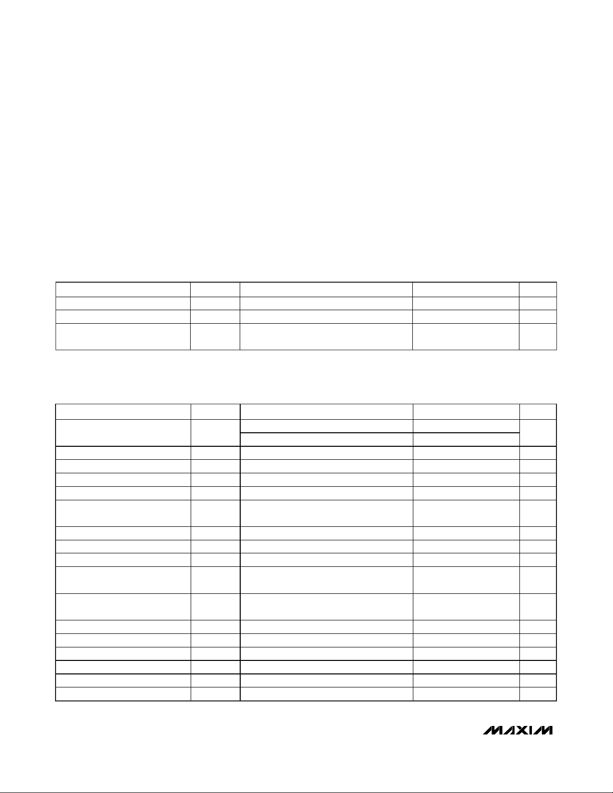
Pin Configuration
Ordering Information
Rev 1; 6/08
For pricing, delivery, and ordering information, please contact Maxim Direct at 1-888-629-4642,
or visit Maxim’s website at www.maxim-ic.com.
+
Denotes a lead-free/RoHS-compliant package.
T&R = Tape and reel.
Typical Operating Circuit appears at end of data sheet.
1-Wire is a registered trademark of Maxim Integrated Products, Inc.
TOP VIEW
LED1
V
+
2
SS
4
DD
5OVD
SS
DS2788
14 LED31LED2
13 LED4
12 LED53DV
PIO
11
10 V
IN
9 SNS6V
8 VMA7DQ
PART TEMP RANGE PIN-PACKAGE
DS2788E+ -25°C to +70°C 14 TSSOP
DS2788E+T&R -25°C to +70°C 14 TSSOP
TSSOP
Page 2
DS2788
Stand-Alone Fuel-Gauge IC with
LED Display Drivers
2 _______________________________________________________________________________________
ABSOLUTE MAXIMUM RATINGS
RECOMMENDED DC OPERATING CHARACTERISTICS
(VDD= 2.5V to 5.5V, TA= -25°C to +70°C, unless otherwise noted. Typical values are at TA= +25°C.)
Stresses beyond those listed under “Absolute Maximum Ratings” may cause permanent damage to the device. These are stress ratings only, and functional
operation of the device at these or any other conditions beyond those indicated in the operational sections of the specifications is not implied. Exposure to
absolute maximum rating conditions for extended periods may affect device reliability.
Voltage Range on Any Pin Relative to V
SS..............
-0.3V to +6.0V
Voltage Range on V
IN
, VMA Relative to V
SS ...
-0.3V to VDD+ 0.3V
DV
SS
to V
SS .....................................................................
-0.3V to +0.3V
LED1–5.................................................................60mA each pin
Operating Temperature Range ...........................-40°C to +85°C
Storage Temperature Range .............................-55°C to +125°C
Soldering Temperature (10s) ................Refer to IPC/JEDEC-020
Specification.
DC ELECTRICAL CHARACTERISTICS
(VDD= 2.5V to 5.5V, TA= -25°C to +70°C, unless otherwise noted. Typical values are at TA= +25°C.)
PARAMETER SYMBOL CONDITIONS MIN TYP MAX UNITS
Supply Voltage VDD (Note 1) +2.5 +5.5 V
VIN, VMA Voltage Range (Note 1) 0 VDD V
DQ, PIO, OVD, LED1–LED5
Voltage Range
(Note 1) 0 +5.5 V
PARAMETER SYMBOL CONDITIONS MIN TYP MAX UNITS
ACTIVE Current I
SLEEP Mode Current I
Input Logic-High: DQ, PIO VIH (Note 1) 1.5 V
Input Logic-Low: DQ, PIO VIL (Note 1) 0.6 V
Output Logic-Low: DQ, PIO, VMA VOL IOL = 4mA (Note 1) 0.4 V
Output Logic-High: VMA VOH IOH = 1mA (Note 1)
VMA Precharge Time t
Pulldown Current: DQ, PIO IPD VDQ, V
Output Logic-Low: LED1–LED5 VOL IOL = -30mA (Note 1) 1 V
Input Logic-High: OVD VIH (Note 1)
Input Logic-Low: OVD VIL (Note 1)
VIN Input Resistance RIN 15 M
DQ SLEEP Timeout t
Undervoltage SLEEP Threshold V
PIO Switch Debounce 100 130 m s
LED1 Displa y Blink Rate 50% duty cycle 0.9 1.0 1.1 Hz
LED Display-On Time 3.6 4.0 4.4 s
ACTIVE
SLEEP
PRE
SLEEP
SLEEP
2.5V VDD 4.2V 70 95
105
1 3 μA
13.3 14.2 ms
= 0.4V 0.2 5 μA
PIO
DQ < VIL 1.8 2.0 2.2 s
(Note 1) 2.40 2.45 2.50 V
V
-
V
DD
0.5
DD
0.2
-
V
V
V
+
SS
0.2
μA
V
Page 3
DS2788
Stand-Alone Fuel-Gauge IC with
LED Display Drivers
_______________________________________________________________________________________ 3
ELECTRICAL CHARACTERISTICS: TEMPERATURE, VOLTAGE, CURRENT
(VCC= 2.5V to 5.5V, TA= -25°C to +70°C, unless otherwise noted. Typical values are at TA= +25°C.)
ELECTRICAL CHARACTERISTICS: 1-Wire INTERFACE, STANDARD
(VCC= 2.5V to 5.5V, TA= -25°C to +70°C.)
PARAMETER SYMBOL CONDITIONS MIN TYP MAX UNITS
Temperature Reso lution T
Temperature Error T
Voltage Reso lution V
Voltage Full-Scale VFS 0 4.992 V
Voltage Error V
Current Resolution I
Current Ful l-Scale IFS ±51.2 mV
Current Ga in Error I
Current Offset Error I
Accumulated Current Offset q
Timebase Error t
0.125 °C
LSB
±3 °C
ERR
4.88 mV
LSB
±50 mV
ERR
1.56 μV
LSB
(Note 2) ±1
GERR
OERR
OERR
ERR
0°C TA +70°C, 2.5V VDD 4.2V
(Notes 3, 4)
0°C TA +70°C, 2.5V VDD 4.2V,
= VSS (Notes 3, 4, 5)
V
SNS
VDD = 3.8V, TA = +25°C ±1
0°C TA +70°C, 2.5V VDD 4.2V ±2
±3
-7.82 +12.5 μV
-188 0
% Full
Scale
μVhr/
day
%
PARAMETER SYMBOL CONDITIONS MIN TYP MAX UNITS
Time Slot t
Recovery Time t
Write-0 Low Time t
Write-1 Low Time t
Read Data Valid t
Reset-Time High t
Reset-Time Low t
Presence-Detect High t
Presence-Detect Low t
60 120 μs
SLOT
1 μs
REC
60 120 μs
LOW0
1 15 μs
LOW1
15 μs
RDV
480 μs
RSTH
480 960 μs
RSTL
15 60 μs
PDH
60 240 μs
PDL
Page 4
DS2788
Stand-Alone Fuel-Gauge IC with
LED Display Drivers
4 _______________________________________________________________________________________
Note 1: All voltages are referenced to VSS.
Note 2: Factory-calibrated accuracy. Higher accuracy can be achieved by in-system calibration by the user.
Note 3: Parameters guaranteed by design.
Note 4: At a constant regulated V
DD
voltage, the Current Offset Bias register can be used to obtain higher accuracy.
Note 5: Accumulation Bias register set to 00h.
Note 6: EEPROM data retention is 10 years at +50°C.
ELECTRICAL CHARACTERISTICS: 1-Wire INTERFACE, OVERDRIVE
(VCC= 2.5V to 5.5V, TA= -25°C to +70°C.)
EEPROM RELIABILITY SPECIFICATION
(VCC= 2.5V to 5.5V, TA= -25°C to +70°C, unless otherwise noted. Typical values are at TA= +25°C.)
PARAMETER SYMBOL CONDITIONS MIN TYP MAX UNITS
Time Slot t
Recovery Time t
Write-0 Low Time t
Write-1 Low Time t
Read Data Valid t
Reset-Time High t
Reset-Time Low t
Presence-Detect High t
Presence-Detect Low t
PARAMETER SYMBOL CONDITIONS MIN TYP MAX UNITS
EEPROM Copy Time t
EEPROM Copy Endurance N
6 16 μs
SLOT
1 μs
REC
6 16 μs
LOW0
1 2 μs
LOW1
2 μs
RDV
48 μs
RSTH
48 80 μs
RSTL
2 6 μs
PDH
8 24 μs
PDL
10 ms
EEC
TA = +50°C (Note 6) 50,000 Cycles
EEC
Page 5
DS2788
Stand-Alone Fuel-Gauge IC with
LED Display Drivers
_______________________________________________________________________________________ 5
Pin Description
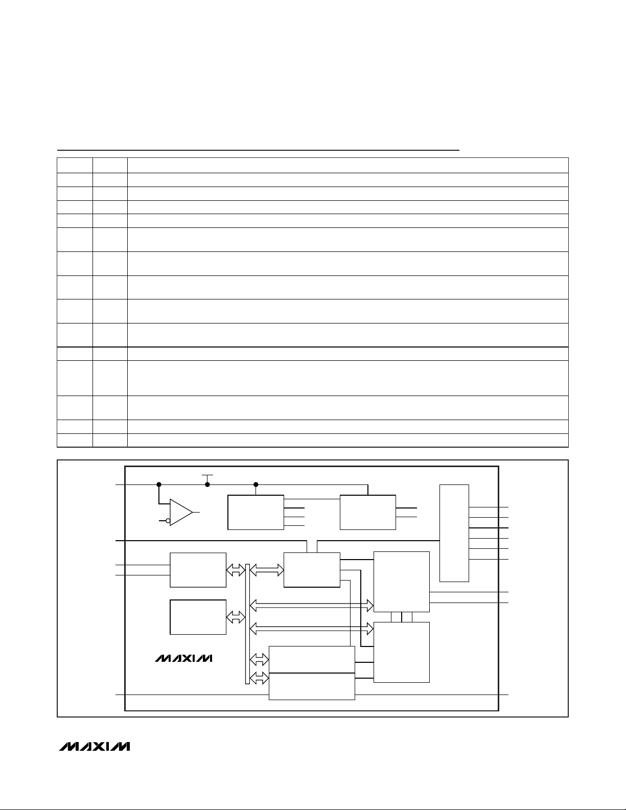
Figure 1. Block Diagram
PIN NAME FUNCTION
1 LED2 Di spla y Driver. Connect to an LED connected to VDD for display of relative pack capacity.
2 LED1 Display Driver. Connect to an LED connected to VDD for display of relative pack capacity.
3 DVSS Display Ground. Ground connection for the LED display drivers. Connect to VSS.
4 VDD Power-Supply Input. Connect to the positive terminal of the battery cel l through a decoupling networ k.
5 OVD
6 V
7 DQ
8 VMA
9 SNS
10 VIN Voltage Sense Input. The voltage of the battery cell is monitored through thi s input p in.
11 PIO
12 LED5
13 LED4 Displa y Driver. Connect to an LED connected to VDD for display of relative pack capacity.
14 LED3 Displa y Driver. Connect to an LED connected to VDD for display of relative pack capacity.
1-Wire Bus Speed Control. Input logic level selects the speed of the 1-Wire bus. Logic 1 selects overdrive (OVD)
and Logic 0 selects standard (STD) timing. On a multidrop bus, all devices must operate at the same speed.
Device Ground. Connect directl y to the negative terminal of the battery cel l. Connect the sen se resi stor
SS
between V
and SNS.
SS
Data Input/Output. 1-Wire data line, open-drain output driver. Connect thi s pin to the DATA terminal of the
battery pac k. This pin has a weak internal pulldown (I
) for sensing pack disconnection from host or charger.
PD
Voltage Measurement Active. Output is driven high before the start of a voltage conversion and driven low at
the end of the conversion cycle.
Sense Resistor Connection. Connect to the negative terminal of the battery pack. Connect the sense resistor
between V
and SNS.
SS
Programmable I/O Pin. Can be configured as input or output to monitor or control u ser-defined external
circuitry. Output driver is open drain. This pin has a weak internal pulldown (IPD). When configured as an input,
upon recognition of a rising edge, the fuel-gauge displa y is enab led.
Display Driver. Connect to an LED connected to V
for display of relative pack capacity. Leave floating in
DD
LED4 conf iguration.
V
DD
PIO
DQ
OVD
SNS
V
POR
EN
1-Wire
INTERFACE
EEPROM
STATUS
AND
CONTROL
ACCUMULATED
CURRENT
TIME BASEBIAS/VREF
LED
DRIVERS
TEMP
AND
VOLTAGE
ADC
RATE AND
TEMPERATURE
COMPENSATION
LED5
LED4
LED3
LED2
LED1
DV
VMA
V
IN
SS
DS2788
CURRENT ADC
15-BIT + SIGN
V
SS
Page 6
DS2788
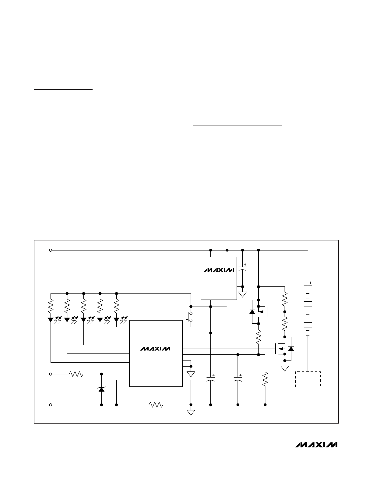
Detailed Description
The DS2788 operates directly from 2.5V to 5.5V and
supports single-cell Li+ battery packs. As shown in
Figure 2, the DS2788 accommodates multicell applications by adding a trim resistor for calibration of an
external voltage-divider for VIN. NV storage is provided
for cell compensation and application parameters.
Host-side development of fuel-gauging algorithms is
eliminated. On-chip algorithms and convenient status
reporting of operating conditions reduce the serial
polling required of the host processor.
Additionally, 16 bytes of EEPROM memory are made
available for the exclusive use of the host system
and/or pack manufacturer. The additional EEPROM
memory can be used to facilitate battery lot and date
tracking and NV storage of system or battery usage
statistics.
A 1-Wire interface provides serial communication at the
standard 16kbps or overdrive 140kbps speeds, allowing access to data registers, control registers, and user
memory. A unique, factory-programmed, 64-bit regis-
tration number (8-bit family code + 48-bit serial number
+ 8-bit CRC) assures that no two parts are alike and
enables absolute traceability. The 1-Wire interface on
the DS2788 supports multidrop capability so that multiple slave devices can be addressed with a single pin.
Power Modes
The DS2788 has two power modes: ACTIVE and
SLEEP. On initial power-up, the DS2788 defaults to
ACTIVE mode. While in ACTIVE mode, the DS2788 is
fully functional with measurements and capacity estimation continuously updated. In SLEEP mode, the
DS2788 conserves power by disabling measurement
and capacity estimation functions, but preserves register contents. SLEEP mode is entered under two different conditions and an enable bit for each condition
makes entry into SLEEP optional. SLEEP mode can be
enabled using the power mode (PMOD) bit or the
undervoltage enable (UVEN) bit.
The PMOD type SLEEP is entered if the PMOD bit is set
and DQ is low for t
SLEEP
(2s nominal). The condition of
DQ low for t
SLEEP
can be used to detect a pack discon-
Stand-Alone Fuel-Gauge IC with
LED Display Drivers
6 _______________________________________________________________________________________
Figure 2. Multicell Application Example
PK+
330Ω330Ω330Ω330Ω330Ω
LEDs
LED1
LED2
LED3
LED4
DS2788
LED5
DATA
PK-
150Ω
5.6V
DQ
SNS
R
SNS
20mΩ
VMA
OVD
DV
MAX6765TTLD2+
RST GND
B3F-1000
PIO
V
DD
V
IN
SS
V
SS
IN ENABLE
OUT TIMEOUT
BSS84
10μF 100kΩ
0.1μF
10kΩ
10kΩ
900kΩ
2N7002
0.1μF
PROTECTION
10-CELL
Li+ BATTERY
CIRCUIT
Page 7
nection or system shutdown, in which no charge or discharge current flows. A PMOD SLEEP condition transitions back to ACTIVE mode when DQ is pulled high.
The second option for entering SLEEP is an undervoltage condition. When the UVEN bit is set, the DS2788
transitions to SLEEP if the voltage on V
IN
is less than
V
SLEEP
(2.45V nominal) and DQ is stable at a low or
high logic level for t
SLEEP
. An undervoltage condition
occurs when a pack is fully discharged, where loading
on the battery should be minimized. UVEN SLEEP
relieves the battery of the I
ACTIVE
load until communi-
cation on DQ resumes.
Note: PMOD and UVEN SLEEP features must be disabled when a battery is charged on an external charger
that does not connect to the DQ pin. PMOD SLEEP can
be used if the charger pulls DQ high. UVEN SLEEP can
be used if the charger toggles DQ. The DS2788
remains in SLEEP and therefore does not measure or
accumulate current when a battery is charged on a
charger that fails to properly drive DQ.
Initiating Communication
in Sleep
When beginning communication with a DS2788 in
PMOD SLEEP, DQ must be pulled up first and then a
1-Wire reset pulse must be issued by the master. In
UVEN SLEEP, the procedure depends on the state of
DQ when UVEN SLEEP was entered. If DQ was low,
DQ must be pulled up and then a 1-Wire reset pulse
must be issued by the master as with PMOD SLEEP. If
DQ was high when UVEN SLEEP was entered, then the
DS2788 is prepared to receive a 1-Wire reset from the
master. In the first two cases with DQ low during
SLEEP, the DS2788
does not respond
to the first rising
edge of DQ with a presence pulse.
Voltage Measurement
Battery voltage is measured at the VINinput with
respect to VSSover a range of 0 to 4.992V, with a resolution of 4.88mV. The result is updated every 440ms
and placed in the Voltage (VOLT) register in two’s complement form. Voltages above the maximum register
value are reported at the maximum value; voltages
below the minimum register value are reported at the
minimum value. Figure 3 shows the format of the
Voltage register.
VINis usually connected to the positive terminal of a
single-cell Li+ battery by a 1kΩ resistor. The input
impedance is sufficiently large (15MΩ) to be connected
to a high-impedance voltage-divider in order to support
multiple-cell applications. The pack voltage should be
divided by the number of series cells to present a single-cell average voltage to the VINinput. In Figure 2,
the value of R can be up to 1MΩ without incurring significant error due to input loading. The VMA pin is driven high t
PRE
before the voltage conversion begins.
This allows an external switching element to enable the
voltage-divider, and allows settling to occur before the
start of the conversion.
DS2788
Stand-Alone Fuel-Gauge IC with
LED Display Drivers
_______________________________________________________________________________________ 7
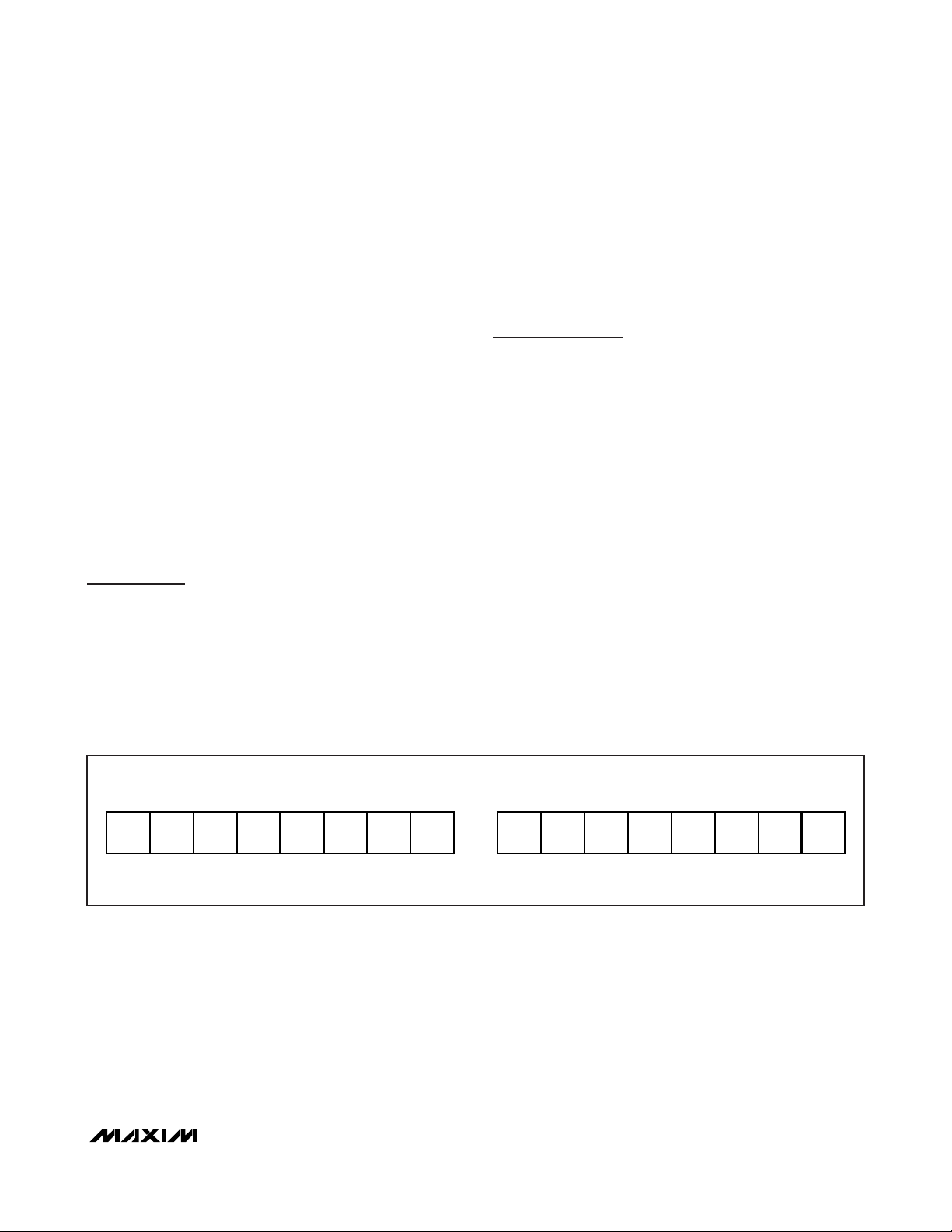
Figure 3. Voltage Register Format
VOLT READ ONLY
MSB—ADDRESS 0Ch LSB—ADD RESS 0Dh
9
S 2
MSb LSb MSb LSb
“S”: SIGN BIT(S), “X”: RESERVED UNITS: 4.88mV
28 27 26 25 24 23 22 21 20 X X X X X
Page 8
DS2788
Temperature Measurement
The DS2788 uses an integrated temperature sensor to
measure battery temperature with a resolution of
0.125°C. Temperature measurements are updated
every 440ms and placed in the Temperature (TEMP)
register in two’s complement form. Figure 4 shows the
format of the Temperature register.
Current Measurement
In the ACTIVE mode of operation, the DS2788 continually measures the current flow into and out of the battery by measuring the voltage drop across a low-value
current-sense resistor, R
SNS
. The voltage-sense range
between SNS and V
SS
is ±51.2mV. The input linearly
converts peak signal amplitudes up to 102.4mV as long
as the continuous signal level (average over the conversion cycle period) does not exceed ±51.2mV. The
ADC samples the input differentially at 18.6kHz and
updates the Current (CURRENT) register at the completion of each conversion cycle.
The Current register is updated every 3.515s with the
current conversion result in two’s complement form.
Charge currents above the maximum register value are
reported at the maximum value (7FFFh = +51.2mV).
Discharge currents below the minimum register value
are reported at the minimum value (8000h = -51.2mV).
Stand-Alone Fuel-Gauge IC with
LED Display Drivers
8 _______________________________________________________________________________________
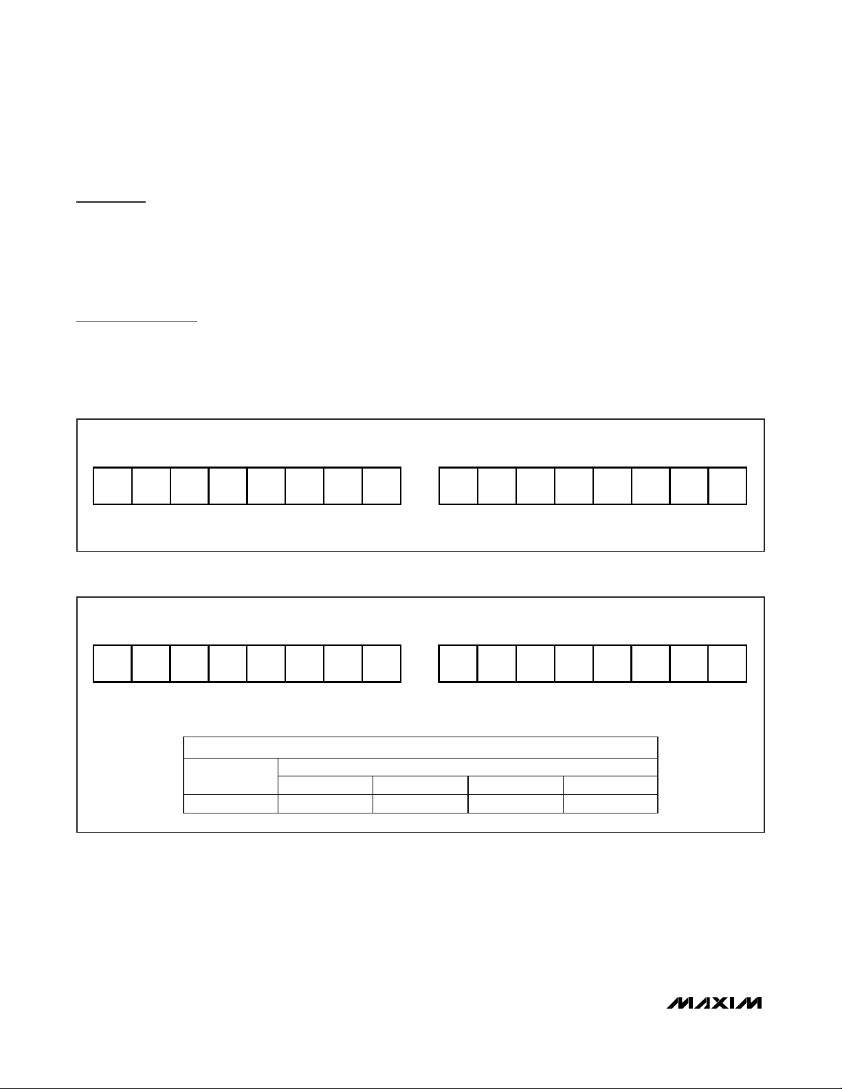
Figure 4. Temperature Register Format
Figure 5. Current Register Format
TEMP READ ONLY
MSB—ADDRESS 0Ah LSB—ADDRESS 0Bh
9
S 2
MSb LSb MSb LSb
“S”: SIGN BIT(S), “X”: RESERVED UNITS: 0.125°C
28 27 26 25 24 23 22 21 20 X X X X X
CURRENT READ ONLY
MSB—ADDRESS 0Eh LSB—ADDRESS 0Fh
14
S 2
MSb LSb MSb LSb
“S”: SIGN BIT(S) UNITS: 1.5625μV/R
213 212 211 210 29 28 27 26 25 24 23 22 21 2
CURRENT RESOLUTION (1 LSB)
R
VSS- V
SNS
1.5625μV 78.13μA 104.2μA 156.3μA 312.5μA
20m 15m 10m 5m
SNS
0
SNS
Page 9
Average Current Measurement
The Average Current (IAVG) register reports an average current level over the preceding 28 seconds. The
register value is updated every 28s in two’s complement form, and is the average of the eight preceding
Current register updates. Figure 6 shows the format of
the Average Current register. Charge currents above
the maximum register value are reported at the maximum value (7FFFh = +51.2mV). Discharge currents
below the minimum register value are reported at the
minimum value (8000h = -51.2mV).
Current Offset Correction
Every 1024th conversion the ADC measures its input
offset to facilitate offset correction. Offset correction
occurs approximately once per hour. The resulting correction factor is applied to the subsequent 1023 measurements. During the offset correction conversion, the
ADC does not measure the sense resistor signal. A
maximum error of 1/1024 in the Accumulated Current
(ACR) register is possible; however, to reduce the
error, the current measurement made just prior to the
offset conversion is displayed in the Current register
and is substituted for the dropped current measurement in the current accumulation process. This results
in an accumulated current error due to offset correction
of less than 1/1024.
Current Offset Bias
The Current Offset Bias (COB) register allows a programmable offset value to be added to raw current measurements. The result of the raw current measurement
plus COB is displayed as the current measurement
result in the Current register, and is used for current
accumulation. COB can be used to correct for a static
offset error, or can be used to intentionally skew the current results and therefore the current accumulation.
COB allows read and write access. Whenever the COB
is written, the new value is applied to all subsequent
current measurements. COB can be programmed in
1.56µV steps to any value between +198.1µV and -
199.7µV. The COB value is stored as a two’s complement value in nonvolatile memory.
Current Measurement
Calibration
The DS2788’s current measurement gain can be
adjusted through the RSGAIN register, which is factorycalibrated to meet the data sheet specified accuracy.
RSGAIN is user accessible and can be reprogrammed
after module or pack manufacture to improve the current measurement accuracy. Adjusting RSGAIN can
correct for variation in an external sense resistor’s nominal value, and allows the use of low-cost, nonprecision
DS2788
Stand-Alone Fuel-Gauge IC with
LED Display Drivers
_______________________________________________________________________________________ 9
Figure 6. Average Current Register Format
Figure 7. Current Offset Bias Register Format
IAVG READ ONLY
MSB—ADDRESS 08h LSB—ADDRESS 09h
14
S 2
MSb LSb MSb LSb
“S”: SIGN BIT(S) UNITS: 1.5625μV/R
COB RW AND EE
ADDRESS 7Bh
S 2
MSb LSb
“S”: SIGN BIT(S) UNITS: 1.56μV/R
213 212 211 210 29 28 27 26 25 24 23 22 21 2
6
25 24 23 22 21 20
SNS
0
SNS
Page 10
DS2788
current-sense resistors. RSGAIN is an 11-bit value
stored in 2 bytes of the parameter EEPROM memory
block. The RSGAIN value adjusts the gain from 0 to
1.999 in steps of 0.001 (precisely 2
-10
). The user must
program RSGAIN cautiously to ensure accurate current
measurement. When shipped from the factory, the gain
calibration value is stored in two separate locations in
the parameter EEPROM block: RSGAIN, which is reprogrammable, and FRSGAIN, which is read only. RSGAIN
determines the gain used in the current measurement.
The read-only FRSGAIN (address B0h and B1h) is provided to preserve the factory value only and is not used
in the current measurement.
Sense Resistor Temperature
Compensation
The DS2788 is capable of temperature compensating
the current-sense resistor to correct for variation in a
sense resistor’s value over temperature. The DS2788 is
factory programmed with the sense resistor temperature
coefficient, RSTC, set to zero, which turns off the temperature compensation function. RSTC is user accessible and can be reprogrammed after module or pack
manufacture to improve the current accuracy when
using a high temperature coefficient current-sense
resistor. RSTC is an 8-bit value stored in the parameter
EEPROM memory block. The RSTC value sets the temperature coefficient from 0 to +7782ppm/°C in steps of
30.5ppm/°C. The user must program RSTC cautiously to
ensure accurate current measurement.
Temperature compensation adjustments are made
when the Temperature register crosses 0.5°C boundaries. The temperature compensation is most effective
with the resistor placed as close as possible to the V
SS
terminal to optimize thermal coupling of the resistor to
the on-chip temperature sensor. If the current shunt is
constructed with a copper PCB trace, run the trace
under the DS2788 package if possible.
Current Accumulation
Current measurements are internally summed, or accumulated, at the completion of each conversion period
with the results displayed in the ACR. The accuracy of
the ACR is dependent on both the current measurement and the conversion time base. The ACR has a
range of 0 to 409.6mVh with an LSb (least significant
bit) of 6.25µVh. Additional read-only registers (ACRL)
hold fractional results of each accumulation to avoid
truncation errors. Accumulation of charge current
above the maximum register value is reported at the
maximum register value (7FFFh); conversely, accumulation of discharge current below the minimum register
value is reported at the minimum value (8000h).
Read and write access is allowed to the ACR. The ACR
must be written MSB (most significant byte) first, then
LSB (least significant byte). The write must be completed within 3.515s (one ACR register update period). A
write to the ACR forces the ADC to perform an offset
correction conversion and update the internal offset
correction factor. Current measurement and accumulation begins with the second conversion following a write
to the ACR. Writing the ACR clears the fractional values
in ACRL. ACR’s format is shown in Figure 8, and
ACRL’s format is shown in Figure 9.
To preserve the ACR value in case of power loss, the
ACR value is backed up to EEPROM. The ACR value is
recovered from EEPROM on power-up. See the memory map in Table 3 for specific address location and
backup frequency.
Stand-Alone Fuel-Gauge IC with
LED Display Drivers
10 ______________________________________________________________________________________
Figure 8. Accumulated Current Register (ACR) Format
ACR R/W AND EE
MSB—ADDRESS 10h LSB—ADDRESS 11h
15
214 213 212 211 210 29 28 27 26 25 24 23 22 21 2
2
MSb LSb MSb LSb
UNITS: 6.25μVh/R
0
SNS
Page 11

Current Blanking
The current blanking feature modifies the current measurement result prior to being accumulated in the ACR.
Current blanking occurs conditionally when a current
measurement (raw current + COB) falls in one of two
defined ranges. The first range prevents charge currents less than 100µV from being accumulated. The
second range prevents discharge currents less than
25µV in magnitude from being accumulated. Chargecurrent blanking is always performed, however, discharge-current blanking must be enabled by setting
the NBEN bit in the Control register. See the register
description for additional information.
Accumulation Bias
The Accumulation Bias (AB) register allows an arbitrary
bias to be introduced into the current-accumulation
process. The AB can be used to account for currents
that do not flow through the sense resistor, estimate
currents too small to measure, estimate battery self-discharge, or correct for static offset of the individual
DS2788 device. The AB register allows a user-programmed positive or negative constant bias to be
included in the current accumulation process. The
user-programmed two’s complement value, with bit
weighting the same as the Current register, is added to
the ACR once per current conversion cycle. The AB
value is loaded on power-up from EEPROM memory.
Figure 10 shows the format of the AB register.
DS2788
Stand-Alone Fuel-Gauge IC with
LED Display Drivers
______________________________________________________________________________________ 11
Figure 9. Fractional/Low Accumulated Current Register (ACRL) Format
Figure 10. Accumulation Bias Register Formats
ACRL READ ONLY
MSB—ADDRESS 12h LSB—ADDRESS 13h
11
2
210 29 28 27 26 25 24 23 22 21 20 X X X X
MSb LSb MSb LSb
“X”: reserved UNITS: 1.526nVHr/R
ACR LSb
R
R
SNS
SNS
VSS- V
SNS
6.25μVh 312.5μAh 416.7μAh 625μAh 1.250mAh
VSS- V
SNS
±409.6mVh ±20.48Ah ±27.30Ah ±40.96Ah ±81.92Ah
AB EE
ADDRESS 61h
20m 15m 10m 5m
ACR RANGE
20m 15m 10m 5m
SNS
6
S 2
MSb LSb
“S”: SIGN BIT(S) UNITS: 1.5625μV/R
25 24 23 22 21 20
SNS
Page 12

DS2788
Capacity Estimation Algorithm
Remaining capacity estimation uses real-time measured values and stored parameters describing the cell
characteristics and application operating limits. Figure
11 describes the algorithm inputs and outputs.
Modeling Cell Stack
Characteristics
To achieve reasonable accuracy in estimating remaining capacity, the cell stack performance characteristics
over temperature, load current, and charge termination
point must be considered. Since the behavior of Li+
cells is nonlinear, these characteristics must be included in the capacity estimation to achieve an acceptable
level of accuracy in the capacity estimation. The
FuelPack™ method used in the DS2788 is described in
general in Application Note 131:
Lithium-Ion Cell Fuel
Gauging with Dallas Semiconductor Battery Monitor
ICs
. To facilitate efficient implementation in hardware, a
modified version of the method outlined in AN131 is
used to store cell characteristics in the DS2788. Full
and empty points are retrieved in a lookup process that
retraces piece-wise linear model consisting of three
Stand-Alone Fuel-Gauge IC with
LED Display Drivers
12 ______________________________________________________________________________________
Figure 11. Top Level Algorithm Diagram
FuelPack is a trademark of Maxim Integrated Products, Inc.
VOLTAGE (R) FULL FULL(T) (R)
TEMPERATURE (R)
CURRENT (R)
ACCUMULATED
CURRENT (ACR) (RW)
AVERAGE CURRENT (R)
CELL PARAMETERS
16 BYTES
(EEPROM)
CAPACITY LOOKUP
AVAILABLE CAPACITY CALCULATION
ACR HOUSEKEEPING
AGE ESTIMATOR
LEARN FUNCTION
ACTIVE EMPTY AE(T) (R)
STANDBY EMPTY SE(T) (R)
REMAINING ACTIVE ABSOLUTE
CAPACITY (RAAC) mAh (R)
REMAINING STANDBY ABSOLUTE
CAPACITY (RSAC) mAh (R)
REMAINING ACTIVE RELATIVE
CAPACITY (RARC) % (R)
REMAINING STANDBY RELATIVE
CAPACITY (RSRC) % (R)
AGING CAPACITY (AC)
(2 BYTES EE)
AGE SCALAR (AS)
(1-BYTE EE)
SENSE RESISTOR PRIME (RSNSP)
(1 -BYTE EE)
CHARGE VOLTAGE (VCHG)
(1-BYTE EE)
MINIMUM CHARGE CURRENT (IMIN)
(1-BYTE EE)
ACTIVE EMPTY VOLTAGE (VAE)
(1-BYTE EE)
ACTIVE EMPTY CURRENT (IAE)
(1-BYTE EE)
Page 13

curves named full, active empty, and standby empty.
Each model curve is constructed with five line segments, numbered 1 through 5. Above +50°C, the segment 5 model curves extend infinitely with zero slope,
approximating the nearly flat change in capacity of Li+
cells at temperatures above +50°C. Segment 4 of each
model curves originates at +50°C on its upper end and
extends downward in temperature to +25°C. Segment
3 joins with segment 2, which in turn joins with segment
1. Segment 1 of each model curve extends from the
junction with segment 2 to infinitely colder temperatures. Segment slopes are stored as µVh ppm change
per °C. The two junctions or breakpoints that join the
segments (labeled TBP12 and TBP23 in Figure 12) are
programmable in 1°C increments from -128°C to
+25°C. They are stored in two’s complement format,
TBP23 at 7Ch, and TBP12 at 7Dh. The slope or derivative for segments 1, 2, 3, and 4 are also programmable.
Full: The full curve defines how the full point of a given
cell stack depends on temperature for a given charge
termination. The charge termination method used in the
application is used to determine the table values. The
DS2788 reconstructs the full line from cell characteristic
table values to determine the full capacity of the battery
at each temperature. Reconstruction occurs in onedegree temperature increments. Full values are stored
as ppm change per °C. For example, if a cell had a
nominal capacity of 1214mAh at +50°C, a full value of
1199mAh at +25°C, and 1182mAh at 0°C (TBP23), the
slope for segment 3 would be:
((1199mAh - 1182mAh) / (1214mAh / 1M)) /
(25°C - 0°C) = 560ppm/°C
1 LSB of the slope registers equals 61ppm so the full
segment 3 slope register (location 0x6Dh) would be
programmed with a value of 0x09h. Each Slope register
has a dynamic range 0ppm to 15555ppm.
DS2788
Stand-Alone Fuel-Gauge IC with
LED Display Drivers
______________________________________________________________________________________ 13
Figure 12. Cell Model Example Diagram
SEGMENT 1
100%
SEGMENT 2
SEGMENT 3 SEGMENT 4
SEGMENT 5
DERIVATIVE
(ppm/°C)
ACTIVE
EMPTY
FULL
STANDBY
EMPTY
CELL
CELL
CHARACTERIZATION
CHARACTERIZATION
+50°C+25°CTBP23TBP12
Page 14

DS2788
Active Empty: The active empty curve defines the temperature variation in the empty point of the discharge
profile based on a high-level load current (one that is
sustained during a high-power operating mode) and
the minimum voltage required for system operation.
This load current is programmed as the active empty
current (IAE), and should be a 3.5s average value to
correspond to values read from the Current register
and the specified minimum voltage, or active empty
voltage (VAE) should be a 250ms average to correspond to values read from the Voltage register. The
DS2788 reconstructs the active empty line from cell
characteristic table values to determine the active
empty capacity of the battery at each temperature.
Reconstruction occurs in one-degree temperature
increments. Active empty segment slopes are stored
the same as described for the full segments.
Standby Empty: The standby empty curve defines the
temperature variation in the empty point in the discharge defined by the application standby current and
the minimum voltage required for standby operation.
Standby empty represents the point that the battery
can no longer support a subset of the full application
operation, such as memory data retention or organizer
functions on a wireless handset. Standby empty segment slopes are stored the same as described for the
full segments.
The standby load current and voltage are used for
determining the cell characteristics but are not programmed into the DS2788. The DS2788 reconstructs
the standby empty line from cell characteristic table
values to determine the standby empty capacity of the
battery at each temperature. Reconstruction occurs in
one-degree temperature increments.
Cell Stack Model Construction
The model is constructed with all points normalized to
the fully charged state at +50°C. The cell parameter
EEPROM block stores the initial values, the +50°C full
value in mVh units, and the +50°C active empty value
as a fraction of the +50°C value. Standby empty at
+50°C is by definition zero and therefore no storage is
required. The slopes (derivatives) of the 4 segments for
each model curve are also stored in the cell parameter
EEPROM block along with the break point temperatures
of each segment. Table 1 shows an example of data
stored in this manner.
Stand-Alone Fuel-Gauge IC with
LED Display Drivers
14 ______________________________________________________________________________________
Table 1. Example Cell Characterization Table (Normalized to +50°C)
Figure 13. Lookup Function Diagram
Manufacturer’s Rated Cell Capacity: 1220mAh
Charge Voltage: 4.2V Charge Current: 500mA Termination Current: 50mA
Active Empty (V, I): 3.0V, 500mA Standby Empty (V, I): 3.0V, 4mA
Sense Resistor: 0.020
SEGMENT BR EAKPOINTS
TBP12 = -12°C
TBP23 = 0°C
CALCULATED VALUE
+50°C NOMINAL
(mAh)
SEGMENT 1
(ppm/°C)
SEGMENT 2
(ppm/°C)
SEGMENT 3
(ppm/°C)
SEGMENT 4
(ppm/°C)
Ful l 1214 488 549 1587 2686
Active Empty 854 1526 2686 3113
Standby Empty 244 183 916 244
CELL MODEL
PARAMETERS
15 BYTES
(EEPROM)
TEMPERATURE
LOOKUP
FUNCTION
FULL(T)
AE(T)
SE(T)
Page 15

Application Parameters
In addition to cell model characteristics, several application parameters are needed to detect the full and
empty points, as well as calculate results in mAh units.
Sense Resistor Prime (RSNSP)
RSNSP stores the value of the sense resistor for use in
computing the absolute capacity results. The value is
stored as a 1-byte conductance value with units of
mhos. RSNSP supports resistor values of 1Ω to
3.922mΩ. RSNSP is located in the parameter EEPROM
block.
Charge Voltage (VCHG)
VCHG stores the charge voltage threshold used to
detect a fully charged state. The value is stored as a
1-byte voltage with units of 19.52mV and can range
from 0 to 4.978V. VCHG should be set marginally less
than the cell voltage at the end of the charge cycle to
ensure reliable charge termination detection. VCHG is
located in the parameter EEPROM block.
Minimum Charge Current (IMIN)
IMIN stores the charge current threshold used to detect
a fully charged state. The value is stored as a 1-byte
value with units of 50µV and can range from 0 to
12.75mV. Assuming R
SNS
= 20mΩ, IMIN can be programmed from 0 to 637.5mA in 2.5mA steps. IMIN
should be set marginally greater than the charge current at the end of the charge cycle to ensure reliable
charge termination detection. IMIN is located in the
parameter EEPROM block.
Active Empty Voltage (VAE)
VAE stores the voltage threshold used to detect the
active empty point. The value is stored in 1 byte with
units of 19.52mV and can range from 0 to 4.978V. VAE
is located in the parameter EEPROM block.
Active Empty Current (IAE)
IAE stores the discharge current threshold used to
detect the active empty point. The unsigned value represents the magnitude of the discharge current and is
stored in 1 byte with units of 200µV and can range from
0 to 51.2mV. Assuming R
SNS
= 20mΩ, IAE can be programmed from 0mA to 2550mA in 10mA steps. IAE is
located in the parameter EEPROM block.
Aging Capacity (AC)
AC stores the rated battery capacity used in estimating
the decrease in battery capacity that occurs in normal
use. The value is stored in 2 bytes in the same units as
the ACR (6.25µVh). Setting AC to the manufacturer’s
rated capacity sets the aging rate to approximately
2.4% per 100 cycles of equivalent full capacity discharges. Partial discharge cycles are added to form
equivalent full capacity discharges. The default estimation results in 88% capacity after 500 equivalent cycles.
The estimated aging rate can be adjusted by setting
AC to a different value than the cell manufacturer’s rating. Setting AC to a lower value, accelerates the estimated aging. Setting AC to a higher value retards the
estimated aging. AC is located in the parameter
EEPROM block.
Age Scalar (AS)
AS adjusts the capacity estimation results downward to
compensate for cell aging. AS is a 1-byte value that
represents values between 49.2% and 100%. The LSB
is weighted at 0.78% (precisely 2-7). A value of 100%
(128 decimal or 80h) represents an unaged battery. A
value of 95% is recommended as the starting AS value
at the time of pack manufacture to allow learning a larger capacity on batteries that have an initial capacity
greater than the nominal capacity programmed in the
cell characteristic table. AS is modified by the cyclecount-based age estimation introduced above and by
the capacity learn function. The host system has read
and write access to AS, however caution should be
exercised when writing AS to ensure that the cumulative aging estimate is not overwritten with an incorrect
value. Typically, it is not necessary for the host to write
AS because the DS2788 automatically saves AS to
EEPROM on a periodic basis. (See the
Memory
section
for details.) The EEPROM-stored value of AS is recalled
on power-up.
Capacity Estimation Utility
Functions
Aging Estimation
As previously discussed, the AS register value is
adjusted occasionally based on cumulative discharge.
As the ACR register decrements during each discharge
cycle, an internal counter is incremented until equal to
32 times AC. AS is then decremented by one, resulting
in a decrease in the scaled full battery capacity of
0.78%. See the AC register description for recommendations on customizing the age estimation rate.
Learn Function
Since Li+ cells exhibit charge efficiencies near unity, the
charge delivered to a Li+ cell from a known empty point
to a known full point is a dependable measure of the
cell capacity. A continuous charge from empty to full
results in a “learn cycle.” First, the active empty point
must be detected. The learn flag (LEARNF) is set at this
point. Second, once charging starts, the charge must
DS2788
Stand-Alone Fuel-Gauge IC with
LED Display Drivers
______________________________________________________________________________________ 15
Page 16

DS2788
continue uninterrupted until the battery is charged to
full. Upon detecting full, LEARNF is cleared, the chargeto-full (CHGTF) flag is set, and the age scalar (AS) is
adjusted according to the learned capacity of the cell.
ACR Housekeeping
The ACR register value is adjusted occasionally to
maintain the coulomb count within the model curve
boundaries. When the battery is charged to full (CHGTF
set), the ACR is set equal to the age-scaled full lookup
value at the present temperature. If a learn cycle is in
progress, correction of the ACR value occurs after the
age scalar (AS) is updated.
When an empty condition is detected (AEF or LEARNF
set), the ACR adjustment is conditional. If AEF is set
and LEARNF is not, the active empty point was not
detected and the battery is likely below the active
empty capacity of the model. The ACR is set to the
active empty model value only if it is greater than the
active empty model value. If LEARNF is set, the battery
is at the active empty point and the ACR is set to the
active empty model value.
Full Detect
Full detection occurs when the voltage (VOLT) readings
remain continuously above the VCHG threshold for the
period between two average current (IAVG) readings,
where both IAVG readings are below IMIN. The two
consecutive IAVG readings must also be positive and
nonzero. This ensures that removing the battery from
the charger does not result in a false detection of full.
Full detect sets the charge-to-full (CHGTF) bit in the
Status (STATUS) register.
Active Empty Point Detect
Active empty point detection occurs when the Voltage
register drops below the VAE threshold and the two
previous current readings are above IAE. This captures
the event of the battery reaching the active empty
point. Note that the two previous current readings must
be negative and greater in magnitude than IAE, that is,
a larger discharge current than specified by the IAE
threshold. Qualifying the voltage level with the discharge rate ensures that the active empty point is not
detected at loads much lighter than those used to construct the model. Also, active empty must not be
detected when a deep discharge at a very light load is
followed by a load greater than IAE. Either case would
cause a learn cycle on the following charge-to-full to
include part of the standby capacity in the measurement of the active capacity. Active empty detection
sets the learn flag bit (LEARNF) in STATUS.
Result Registers
The DS2788 processes measurement and cell characteristics on a 3.5s interval and yields seven result registers. The result registers are sufficient for direct display
to the user in most applications. The host system can
produce customized values for system use or user display by combining measurement, result, and user
EEPROM values.
FULL(T): The full capacity of the battery at the present
temperature is reported normalized to the +50°C full
value. This 15-bit value reflects the cell model full value
at the given temperature. FULL(T) reports values
between 100% and 50% with a resolution of 61ppm
(precisely 2
-14
). Though the register format permits values greater than 100%, the register value is clamped to
a maximum value of 100%.
Active Empty, AE(T): The active empty capacity of the
battery at the present temperature is reported normalized to the +50°C full value. This 13-bit value reflects
the cell model active empty at the given temperature.
AE(T) reports values between 0% and 49.8% with a
resolution of 61ppm (precisely 2
-14
).
Standby Empty, SE(T): The standby empty capacity of
the battery at the present temperature is reported normalized to the +50°C full value. This 13-bit value
reflects the cell model standby empty value at the current temperature. SE(T) reports values between 0% and
49.8% with a resolution of 61ppm (precisely 2
-14
).
Remaining Active Absolute Capacity, RAAC [mAh]:
RAAC reports the capacity available under the current
temperature conditions at the active empty discharge
rate (IAE) to the active empty point in absolute units of
milliamp/hours (mAh). RAAC is 16 bits. See Figure 14.
Remaining Standby Absolute Capacity, RSAC [mAh]:
RSAC reports the capacity available under the current
temperature conditions at the standby empty discharge
rate (ISE) to the standby empty point capacity in
absolute units of mAh. RSAC is 16 bits. See Figure 15.
Remaining Active Relative Capacity, RARC [%]:
RARC reports the capacity available under the current
temperature conditions at the active empty discharge
rate (IAE) to the active empty point in relative units of
percent. RARC is 8 bits. See Figure 16.
Remaining Standby Relative Capacity, RSRC [%]:
RSRC reports the capacity available under the current
temperature conditions at the standby empty discharge
rate (ISE) to the standby empty point capacity in relative units of percent. RSRC is 8 bits. See Figure 17.
Stand-Alone Fuel-Gauge IC with
LED Display Drivers
16 ______________________________________________________________________________________
Page 17

DS2788
Stand-Alone Fuel-Gauge IC with
LED Display Drivers
______________________________________________________________________________________ 17
Figure 14. Remaining Active Absolute Capacity Register Format
Figure 15. Remaining Standby Absolute Capacity Register Format
Figure 16. Remaining Active Relative Capacity Register Format
Figure 17. Remaining Standby Relative Capacity Register Format
RAAC READ ONLY
MSB—ADDRESS 02h LSB—ADDRESS 03h
15
214 213 212 211 210 29 28 27 26 25 24 23 22 21 2
2
MSb LSb MSb LSb
UNITS: 1.6mAhr
RSAC READ ONLY
MSB—ADDRESS 04h LSB—ADDRESS 05h
14
213 212 211 210 29 28 27 26 25 24 23 22 21 2
2
LSb MSb LSb
UNITS: 1.6mAhr
RARC RE AD ONLY
ADDRESS 06h
7
2
MSb LSb
UNITS: 1%
26 25 24 23 22 21 20
0
0
RSRC READ ONLY
ADDRESS 07h
7
2
MSb LSb
UNITS: 1%
26 25 24 23 22 21 20
Page 18

DS2788
Stand-Alone Fuel-Gauge IC with
LED Display Drivers
18 ______________________________________________________________________________________
The Status register contains bits that report the device
status. The bits can be set internally by the DS2788.
The CHGTF, AEF, SEF, LEARNF, and VER bits are
read-only bits that can be cleared by hardware. The
UVF and PORF bits can only be cleared through the
1-Wire interface.
*This bit can be set by the DS2788, and can only be cleared through the 1-Wire interface.
**LEARNF is only cleared if ACR reaches 0 after VOLT < VAE.
Figure 18. Status Register Format
Calculation of Results
RAAC [mAh] = (ACR[mVh] - AE(T) × FULL50[mVh]) × RSNSP [mhos]
RSAC [mAh] = (ACR[mVh] - SE(T) × FULL50[mVh]) × RSNSP [mhos]
RARC [%] = 100% × (ACR[mVh] - AE(T) × FULL50[mVh]) / {(AS × FULL(T) - AE(T)) × FULL50[mVh]}
RSRC [%] = 100% × (ACR[mVh] - SE(T) × FULL50[mVh]) / {(AS × FULL(T) - SE(T)) × FULL50[mVh]}
Status Register
ADDRESS 01h BIT DEFINITION
Field Bit Format Allowable Values
Charge Termination F lag
CHGTF 7 Read Only
AEF 6 Read Only
Set to 1 when: (VOLT > VCHG) and (0 < IAVG < IMIN) continuously for a period
between two IAVG register updates (28s to 56s).
Cleared to 0 when: RA RC < 90%
Active Empty Flag
Set to 1 when: VOLT < VAE
Cleared to 0 when: RA RC > 5%
Standby Empty Flag
SEF 5 Read Only
LEARNF 4 Read Only
Reserved 3 Read Only Undefined
UVF 2 Read/Write*
PORF 1 Read/Write*
Reserved 0 Read Only Undefined
Set to 1 when: RSRC < 10%
Cleared to 0 when: RSRC > 15%
Learn Flag—When set to 1, a charge cycle can be used to learn battery capacity.
Set to 1 when: (VOLT falls from above VAE to below VAE) and (CURRENT > IAE)
Cleared to 0 when: (CHGTF = 1) or (CURRENT < 0) or (ACR = 0**) or (ACR
written or recalled from EEPROM) or (SLEEP Entered).
Undervoltage Flag
Set to 1 when: VOLT < V
Cleared to 0 by: User
Power-On Reset Flag—Useful for reset detection, see text below.
Set to 1 when: upon power-up by hardware.
Cleared to 0 by: User
SLEEP
Page 19

DS2788
Stand-Alone Fuel-Gauge IC with
LED Display Drivers
______________________________________________________________________________________ 19
All Control register bits are read and write accessible.
The Control register is recalled from parameter
EEPROM memory at power-up. Register bit values can
be modified in shadow RAM after power-up. Shadow
RAM values can be saved as the power-up default values by using the Copy Data command.
Control Register
Figure 19. Control Register Format
ADDRESS 60h BIT DEFINITION
Field Bit Format Allowable Values
Negative Blan king Enable
NBEN 7 Read/Write
UVEN 6 Read/Write
PMOD 5 Read/Write
RNAOP 4 Read/Write
DC 3 Read/Write
Reserved 0:2 Undefined
0: Allows negative current readings to always be accumulated.
1: Enables blanking of negative current readings up to -25μV.
Undervoltage SLEEP Enable
0: Disables transition to SLEEP mode based on V
1: Enabl es transition to SLEEP mode if V
logic level for t
Power Mode Enable
0: Disables trans ition to SLEEP mode based on DQ logic state.
1: Enables tran sit io n to SLEEP mode if DQ is at a logic- low for t
Read Net Address Op Code
0: Read net addres s command = 33h.
1: Read net addres s command = 39h.
Display Control
0: Enables LED5 fuel-gauge display.
1: Enables LED4 fuel-gauge display.
SLEEP.
voltage.
IN
< V
IN
and DQ are stable at either
SLEE P
SLEEP.
Page 20

DS2788
Stand-Alone Fuel-Gauge IC with
LED Display Drivers
20 ______________________________________________________________________________________
Fuel-Gauge Display
The DS2788 provides five open-drain drivers capable
of sinking 30mA. These can be used to directly drive
either 4 or 5 LEDs to display Remaining Active Relative
Pack Capacity (RARC). The LEDs are enabled when
the PIO is configured as an input and the PIO pin recognizes a rising edge. The display lights for 4s and
then is disabled regardless of the state of the PIO pin.
Further presses or releases of the button connected to
the PIO pin after the 100ms debounce delay causes
the display to be enabled (the display does not light
continuously if the button is held down).
Table 2 summarizes how the LEDs are enabled. B signifies that the LED is blinking at a 50% duty cycle, 0.5s
on, 0.5s off, to be repeated for the display time of 4s. L
signifies the pin is pulled low, and the LED is lit. X signifies the pin is high impedance, and the LED is unlit.
Table 2. Fuel-Gauge Display Summary
Special Feature Register
Figure 20. Special Feature Register Format
All Special Feature register bits are read and write accessible, with default values specified in each bit definition.
ADDRESS 15h BIT DEFINITION
Field Bit Format Allowable Values
Reserved 1:7 Undefined
PIO Sense and Control
Read values:
0: PIO pin V
1: PIO pin V
PIOSC 0 Read/Write
Write va lue s:
0: Activates PIO pin open-drain output driver, forcing the PIO pin low.
1: Disables the output dri ver, allowing the PIO pin to be pulled high or used as
an input.
Power-up and SLEEP mode default: 1 (PIO pin is high-Z).
Note: PIO pin has weak pulldown.
IL
IH
CAPACITY
RARC 10 XXXXB XXXB
10 < RARC 20 XXXXL XXXL
20 < RARC 25 XXXLL XXXL
25 < RARC 40 XXXLL XXLL
40 < RARC 50 XXLLL XXLL
50 < RARC 60 XXLLL XLLL
60 < RARC 75 XLLLL XLLL
75 < RARC 80 XLLLL LLLL
80 < RARC 100 LLLLL LLLL
5 LEDs, DC: 0
LED5–LED1
4 LEDs, DC: 1
LED4–LED1
Page 21

DS2788
Stand-Alone Fuel-Gauge IC with
LED Display Drivers
______________________________________________________________________________________ 21
The EEPROM register provides access control of the
EEPROM blocks. EEPROM blocks can be locked to prevent alteration of data within the block. Locking a block
disables write access to the block. Once a block is
locked, it cannot be unlocked. Read access to EEPROM
blocks is unaffected by the lock/unlock status.
EEPROM Register
Figure 21. EEPROM Register Format
ADDRESS 1Fh BIT DEFINITION
Field Bit Format Allowable Values
EEPROM Copy Flag
Set to 1 when: Copy Data command executed.
EEC 7 Read Only
LOCK 6
Reserved 2:6 Undefined
BL1 1 Read Only
BL0 0 Read Only
Read/Write
to 1
Cleared to 0 when: Copy Data command completes.
Note: Whi le EEC = 1, writes to EEPROM addresse s are ignored.
Power-up default: 0
EEPROM Lock Enable
Host write to 1: Enables the Lock command. Host must issue Lock command as
next command after writing loc k enable bit to 1.
Cleared to 0 when: Loc k command completes or when Lock command is not the
command issued immediately fo llowing the Write command used to set the lock
enable bit.
Power-up default: 0
EEPROM Block 1 Lock Flag (Parameter EEPROM 60h–7Fh)
0: EEPROM is not locked.
1: EEPROM block is locked.
Factor y default: 0
EEPROM Block 0 Lock Flag (User EEPROM 20h–2Fh)
0: EEPROM is not locked.
1: EEPROM block is locked.
Factor y default: 0
Page 22

DS2788
Stand-Alone Fuel-Gauge IC with
LED Display Drivers
22 ______________________________________________________________________________________
Memory
The DS2788 has a 256-byte linear memory space with
registers for instrumentation, status, and control, as well
as EEPROM memory blocks to store parameters and
user information. Byte addresses designated as
“Reserved” return undefined data when read. Reserved
bytes should not be written. Several byte registers are
paired into two-byte registers in order to store 16-bit values. The MSB of the 16-bit value is located at a even
address and the LSB is located at the next address
(odd) byte. When the MSB of a two-byte register is read,
the MSB and LSB are latched simultaneously and held
for the duration of the Read-Data command to prevent
updates to the LSB during the read. This ensures synchronization between the two register bytes. For consistent results, always read the MSB and the LSB of a
two-byte register during the same read data command
sequence.
EEPROM memory consists of the NV EEPROM cells overlaid with volatile shadow RAM. The Read Data and Write
Data commands allow the 1-Wire interface to directly
accesses only the shadow RAM. The Copy Data and
Recall Data function commands transfer data between
the shadow RAM and the EEPROM cells. To modify the
data stored in the EEPROM cells, data must be written to
the shadow RAM and then copied to the EEPROM. To
verify the data stored in the EEPROM cells, the EEPROM
data must be recalled to the shadow RAM and then read
from the shadow RAM.
User EEPROM
A 16-byte user EEPROM memory (block 0, addresses
20h–2Fh) provides NV memory that is uncommitted to
other DS2788 functions. Accessing the user EEPROM
block does not affect the operation of the DS2788. User
EEPROM is lockable, and once locked, write access is
not allowed. The battery pack or host system manufacturer can program lot codes, date codes, and other
manufacturing, warranty, or diagnostic information and
then lock it to safeguard the data. User EEPROM can
also store parameters for charging to support different
size batteries in a host device as well as auxiliary model
data such as time to full charge estimation parameters.
Parameter EEPROM
Model data for the cells and application operating
parameters are stored in the parameter EEPROM memory (block 1, addresses 60h–7Fh). The ACR (MSB and
LSB) and AS registers are automatically saved to EEPROM when the RARC result crosses 4% boundaries.
This allows the DS2788 to be located outside the protection FETs. In this manner, if a protection device is
triggered, the DS2788 cannot lose more that 4% of
charge or discharge data.
Table 3. Memory Map
ADDRESS (HEX) DESCRIPTION READ/WRITE
00 Reserved R
01 STATUS: Status Register R/W
02 RAAC: Remaining Active Absolute Capacity MSB R
03 RAAC: Remaining Active Absolute Capacity LSB R
04 RSAC: Remaining Standby Absolute Capacit y MSB R
05 RSAC: Remaining Standby Absolute Capacit y LSB R
06 RARC: Remaining Active Relative Capacity R
07 RSRC: Remaining Standby Relative Capacity R
08 IAVG: Average Current Register MSB R
09 IAVG: Average Current Register LSB R
0A TEMP: Temperature Register MSB R
0B TEMP: Temperature Register LSB R
0C VOLT: Voltage Register MSB R
0D VOLT: Voltage Register LSB R
0E CURRENT: Current Register MSB R
0F CURRENT: Current Register LSB R
10 ACR: Accumulated Current Register MSB R/W*
11 ACR: Accumulated Current Register LSB R/W*
Page 23

DS2788
Stand-Alone Fuel-Gauge IC with
LED Display Drivers
______________________________________________________________________________________ 23
Table 3. Memory Map (continued)
Table 4. Parameter EEPROM Memory Block 1
*Register value is automatically saved to EEPROM during ACTIVE mode operation and recalled from EEPROM on power-up.
ADDRESS (HEX) DESCRIPTION READ/WRITE
12 ACRL: Low Accumulated Current Register MSB R
13 ACRL: Low Accumulated Current Register LSB R
14 AS: Age Scalar R/W*
15 SFR: Special Feature Register R/W
16 FULL: Full Capacity MSB R
17 FULL: Full Capacit y LSB R
18 AE: Active Empty MSB R
19 AE: Active Empty LSB R
1A SE: Standby Empty MSB R
1B SE: Standby Empty LSB R
1C to 1E Reserved —
1F EEPROM: EEPROM Register R/W
20 to 2F User EEPROM, Lockable, Block 0 R/W
30 to 5F Reserved —
60 to 7F Parameter EEPROM, Loc kable, Block 1 R/W
80 to AD Reserved —
AE FVGAIN: Factory Voltage Gain MSB R
AF FVGAIN: Factory Voltage Gain LSB R
B0 FRSGAIN: Factory Sense Re si stor Gain MS B R
B1 FRSGAIN: Factory Sense Re si stor Gain LSB R
B2 to FF Reserved —
ADDRESS (HEX) DESCRIPTION ADDRESS (HEX) DESCRIPTION
60 CONTROL: Control Register 70 AE Segment 4 Slope
61 AB: Accumulation Bias 71 AE Segment 3 Slope
62 AC: Aging Capacity MSB 72 AE Segment 2 Slope
63 AC: Aging Capacity LSB 73 AE Segment 1 Slope
64 VCHG: Charge Voltage 74 SE Segment 4 S lope
65 IMIN: Minimum Charge Current 75 SE Segment 3 Slope
66 VAE: Active Empty Voltage 76 SE Segment 2 Slope
67 IAE: Acti ve Empty Current 77 SE Segment 1 Slope
68 Active Empty 50 78 RSGAIN: Sense Resistor Gain MSB
69 RSNSP: Sense Resi stor Prime 79 RSGAIN: Sense Resistor Gain LSB
6A Full 50 MSB 7A RSTC: Sense Res istor Temp Coeff icient
6B Full 50 LSB 7B COB: Current Offset Bias
6C Full Segment 4 S lope 7C TBP 23
6D Full Segment 3 S lope 7D TBP 12
6E Full Segment 2 Slope 7E VGAIN: Voltage Gain MSB
6F Full Segment 1 Slope 7F VGAIN: Voltage Gain LSB
Page 24

DS2788
Stand-Alone Fuel-Gauge IC with
LED Display Drivers
24 ______________________________________________________________________________________
1-Wire Bus System
The 1-Wire bus is a system that has a single bus master and one or more slaves. A multidrop bus is a 1-Wire
bus with multiple slaves. A single-drop bus has only
one slave device. In all instances, the DS2788 is a
slave device. The bus master is typically a microprocessor in the host system. The discussion of this
bus system consists of four topics: 64-bit net address,
hardware configuration, transaction sequence, and
1-Wire signaling.
64-Bit Net Address
Each DS2788 has a unique, factory-programmed
1-Wire net address that is 64 bits in length. The first
eight bits are the 1-Wire family code (32h for DS2788).
The next 48 bits are a unique serial number. The last
eight bits are a cyclic redundancy check (CRC) of the
first 56 bits (see Figure 22). The 64-bit net address and
the 1-Wire I/O circuitry built into the device enable the
DS2788 to communicate through the 1-Wire protocol
detailed in the
1-Wire Bus System
section.
CRC Generation
The DS2788 has an 8-bit CRC stored in the MSB of its
1-Wire net address. To ensure error-free transmission
of the address, the host system can compute a CRC
value from the first 56 bits of the address and compare
it to the CRC from the DS2788. The host system is
responsible for verifying the CRC value and taking
action as a result. The DS2788 does not compare CRC
values and does not prevent a command sequence
from proceeding as a result of a CRC mismatch. Proper
use of the CRC can result in a communication channel
with a very high level of integrity.
The CRC can be generated by the host using a circuit
consisting of a shift register and XOR gates as shown
in Figure 23, or it can be generated in software.
Additional information about the Maxim 1-Wire CRC is
available in Application Note 27:
Understanding and
Using Cyclic Redundancy Checks with Maxim iButton
Products
.
In the circuit in Figure 23, the shift register bits are initialized to 0. Then, starting with the LSb of the family
code, one bit at a time is shifted in. After the 8th bit of
the family code has been entered, then the serial number is entered. After the 48th bit of the serial number
has been entered, the shift register contains the CRC
value.
Hardware Configuration
Because the 1-Wire bus has only a single line, it is
important that each device on the bus be able to drive
it at the appropriate time. To facilitate this, each device
attached to the 1-Wire bus must connect to the bus
with open-drain or three-state output drivers. The
DS2788 uses an open-drain output driver as part of the
bidirectional interface circuitry shown in Figure 24. If a
bidirectional pin is not available on the bus master,
separate output and input pins can be connected
together.
Figure 22. 1-Wire Net Address Format
Figure 23. 1-Wire CRC Generation Block Diagram
i
Button is a registered trademark of Maxim Integrated Products, Inc.
8-BIT CRC 48-BIT SERIAL NUMBER
MSb LSb
MSb XOR XOR
8-BIT FAMILY
CODE (32h)
INPUT
LSb
XOR
Page 25

DS2788
Stand-Alone Fuel-Gauge IC with
LED Display Drivers
______________________________________________________________________________________ 25
The 1-Wire bus must have a pullup resistor at the busmaster end of the bus. For short line lengths, the value
of this resistor should be approximately 5kΩ. The idle
state for the 1-Wire bus is high. If, for any reason, a bus
transaction must be suspended, the bus must be left in
the idle state to properly resume the transaction later. If
the bus is left low for more than 120µs (16µs for overdrive speed), slave devices on the bus begin to interpret the low period as a reset pulse, effectively
terminating the transaction.
The DS2788 can operate in two communication speed
modes, standard and overdrive. The speed mode is
determined by the input logic level of the OVD pin with
a logic 0 selecting standard speed and a logic 1
selecting overdrive speed. The OVD pin must be at a
stable logic level of 0 or 1 before initializing a transaction with a reset pulse. All 1-Wire devices on a multinode bus must operate at the same communication
speed for proper operation. 1-Wire timing for both standard and overdrive speeds are listed in the
Electrical
Characteristics: 1-Wire Interface
tables.
Transaction Sequence
The protocol for accessing the DS2788 through the
1-Wire port is as follows:
• Initialization
• Net Address Command
• Function Command
• Transaction/Data
The sections that follow describe each of these steps in
detail.
All transactions of the 1-Wire bus begin with an initialization sequence consisting of a reset pulse transmitted
by the bus master, followed by a presence pulse simultaneously transmitted by the DS2788 and any other
slaves on the bus. The presence pulse tells the bus
master that one or more devices are on the bus and
ready to operate. For more details, see the
1-Wire
Signaling
section.
Net Address Commands
Once the bus master has detected the presence of one
or more slaves, it can issue one of the net address
commands described in the following paragraphs. The
name of each ROM command is followed by the 8-bit
op code for that command in square brackets.
Figure 25 presents a transaction flowchart of the net
address commands.
Read Net Address [33h or 39h]. This command allows
the bus master to read the DS2788’s 1-Wire net
address. This command can only be used if there is a
single slave on the bus. If more than one slave is present, a data collision occurs when all slaves try to transmit at the same time (open drain produces a
wired-AND result). The RNAOP bit in the Status register
selects the op code for this command, with RNAOP = 0
indicating 33h and RNAOP = 1 indicating 39h.
Figure 24. 1-Wire Bus Interface Circuitry
BUS MASTER
Rx
Tx
V
PULLUP
(2.0V TO 5.5V)
4.7kΩ
Rx = RECEIVE
Tx = TRANSMIT
0.2μA
(TYP)
DS2788 1-Wire PORT
Rx
Tx
100Ω MOSFET
Page 26

DS2788
Stand-Alone Fuel-Gauge IC with
LED Display Drivers
26 ______________________________________________________________________________________
Match Net Address [55h]. This command allows the
bus master to specifically address one DS2788 on the
1-Wire bus. Only the addressed DS2788 responds to
any subsequent function command. All other slave
devices ignore the function command and wait for a
reset pulse. This command can be used with one or
more slave devices on the bus.
Skip Net Address [CCh]. This command saves time
when there is only one DS2788 on the bus by allowing
the bus master to issue a function command without
specifying the address of the slave. If more than one
slave device is present on the bus, a subsequent function command can cause a data collision when all
slaves transmit data at the same time.
Search Net Address [F0h]. This command allows the
bus master to use a process of elimination to identify
the 1-Wire net addresses of all slave devices on the
bus. The search process involves the repetition of a
simple three-step routine: read a bit, read the complement of the bit, then write the desired value of that bit.
The bus master performs this simple three-step routine
on each bit location of the net address. After one complete pass through all 64 bits, the bus master knows
the address of one device. The remaining devices can
then be identified on additional iterations of the
process. See Chapter 5 of the
Book of iButton
Standards
for a comprehensive discussion of a net
address search, including an actual example
(www.maxim-ic.com/ibuttonbook
).
Resume [A5h]. This command increases data throughput in multidrop environments where the DS2788 needs
to be accessed several times. Resume is similar to the
Skip Net Address command in that the 64-bit net
address does not have to be transmitted each time the
DS2788 is accessed. After successfully executing a
Match Net Address command or Search Net Address
command, an internal flag is set in the DS2788. When
the flag is set, the DS2788 can be repeatedly accessed
through the Resume command function. Accessing
another device on the bus clears the flag, thus preventing two or more devices from simultaneously responding to the Resume command function.
Function Commands
After successfully completing one of the net address
commands, the bus master can access the features of
the DS2788 with any of the function commands
described in the following paragraphs. The name of
each function is followed by the 8-bit op code for that
command in square brackets. Table 5 summarizes the
function commands.
Read Data [69h, XX]. This command reads data from
the DS2788 starting at memory address XX. The LSb of
the data in address XX is available to be read immediately after the MSb of the address has been entered.
Because the address is automatically incremented after
the MSb of each byte is received, the LSb of the data at
address XX + 1 is available to be read immediately
after the MSb of the data at address XX. If the bus master continues to read beyond address FFh, data is read
starting at memory address 00 and the address is automatically incremented until a reset pulse occurs.
Addresses labeled “Reserved” in the memory map
contain undefined data values. The read data command can be terminated by the bus master with a reset
pulse at any bit boundary. Reads from EEPROM block
addresses return the data in the shadow RAM. A Recall
Data command is required to transfer data from the
EEPROM to the shadow. See the
Memory
section for
more details.
Write Data [6Ch, XX]. This command writes data to the
DS2788 starting at memory address XX. The LSb of the
data to be stored at address XX can be written immediately after the MSb of address has been entered.
Because the address is automatically incremented after
the MSb of each byte is written, the LSb to be stored at
address XX + 1 can be written immediately after the
MSb to be stored at address XX. If the bus master continues to write beyond address FFh, the data starting at
address 00 is overwritten. Writes to read-only addresses, reserved addresses, and locked EEPROM blocks
are ignored. Incomplete bytes are not written. Writes to
unlocked EEPROM block addresses modify the shadow RAM. A Copy Data command is required to transfer
data from the shadow to the EEPROM. See the
Memory
section for more details.
Page 27

DS2788
Stand-Alone Fuel-Gauge IC with
LED Display Drivers
______________________________________________________________________________________ 27
Copy Data [48h, XX]. This command copies the con-
tents of the EEPROM shadow RAM to EEPROM cells for
the EEPROM block containing address XX. Copy data
commands that address locked blocks are ignored.
While the copy data command is executing, the EEC bit
in the EEPROM register is set to 1 and writes to
EEPROM addresses are ignored. Reads and writes to
non-EEPROM addresses can still occur while the copy
is in progress. The copy data command takes t
EEC
time
to execute, starting on the next falling edge after the
address is transmitted.
Recall Data [B8h, XX]. This command recalls the contents of the EEPROM cells to the EEPROM shadow
memory for the EEPROM block containing address XX.
Lock [6Ah, XX]. This command locks (write protects)
the block of EEPROM memory containing memory
address XX. The lock bit in the EEPROM register must
be set to 1 before the lock command is executed. To
help prevent unintentional locks, one must issue the
lock command immediately after setting the lock bit
(EEPROM register, address 1Fh, bit 06) to a 1. If the
lock bit is 0 or if setting the lock bit to 1 does not immediately precede the lock command, the lock command
has no effect. The lock command is permanent; a
locked block can never be written again.
Table 5. Function Commands
COMMAND DESCRIPTION
Read Data Reads data from memory starting at address XX. 69h, XX Master Rx
Write Data Writes data to memory starting at address XX. 6Ch, XX Master Tx
Copy Data
Recall Data Recalls EEPROM block containing address XX to RAM. B8h, XX Master Reset None
Lock
Copies shadow RAM data to EEPROM block containing
address XX.
Permanently loc ks the block of EEPROM
containing address XX.
COMMAND
PROTOCOL
48h, XX Master Reset None
6Ah, XX Master Reset None
BUS STATE AFTER
COMMAND
PROTOCOL
BUS DATA
bytes of data
bytes of data
Up to 256
Up to 256
Page 28
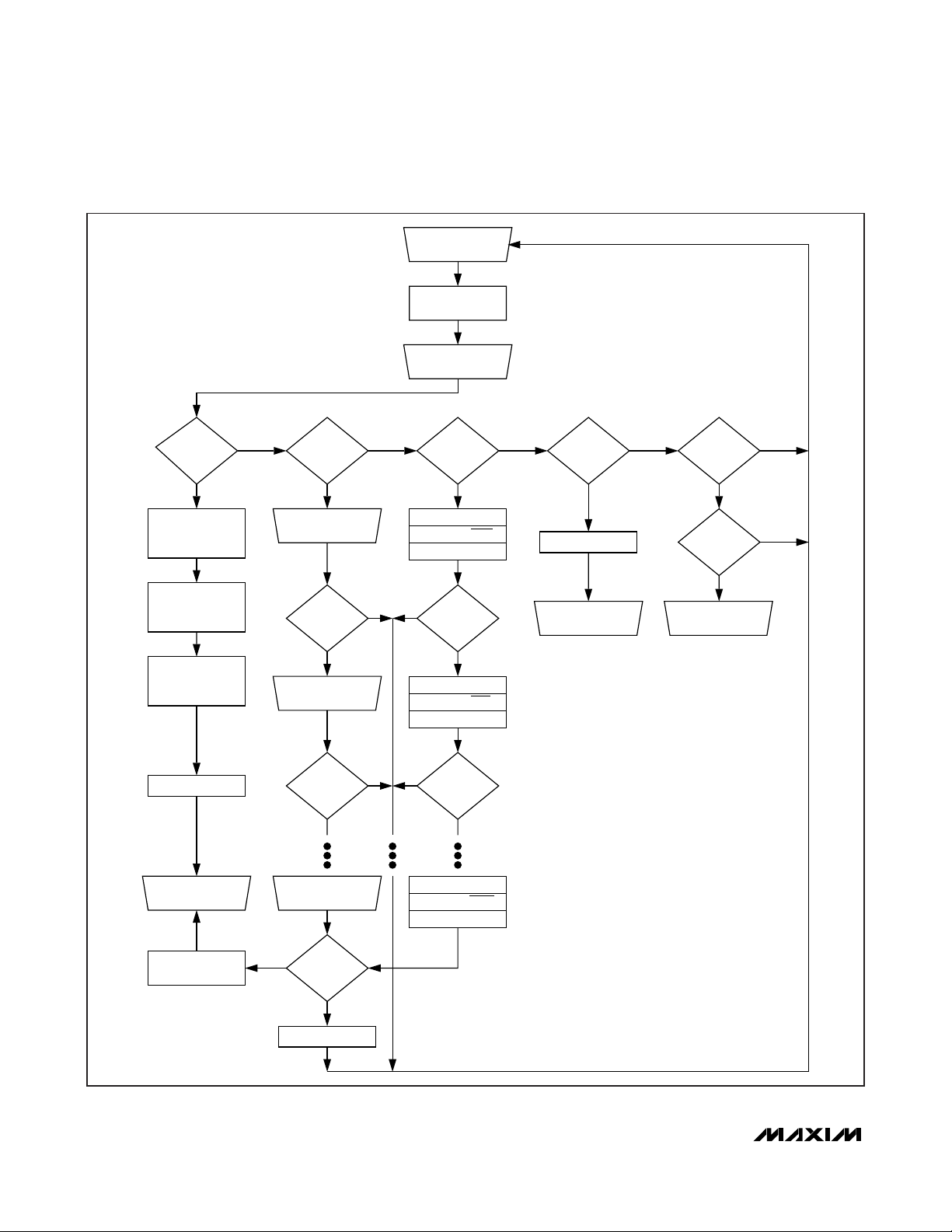
DS2788
Stand-Alone Fuel-Gauge IC with
LED Display Drivers
28 ______________________________________________________________________________________
Figure 25. Net Address Command Flowchart
MASTER Tx
RESET PULSE
DS2788 Tx
PRESENCE PULSE
FAMILY CODE
SERIAL NUMBER
CLEAR RESUME
33h/39h
READ
YES
DS2788 Tx
1 BYTE
DS2788 Tx
6 BYTES
DS2788 Tx
CRC
1 BYTE
NO
55h
MATCH
YES
MASTER Tx
BIT 0
BIT O
MATCH?
YES
MASTER Tx
BIT 1
BIT 1
MATCH?
NO
NO NO
NO NO
MASTER Tx NET
ADDRESS COMMAND
F0h
SEARCH
YES
DS2788 Tx BIT 0
DS2788 Tx BIT 0
MASTER Tx BIT 0
BIT O
MATCH?
YES
DS2788 Tx BIT 1
DS2788 Tx BIT 1
MASTER Tx BIT 1
BIT 1
MATCH?
NO NO NO
CCh
SKIP
YES
CLEAR RESUME
MASTER Tx
FUNCTION COMMAND
A5h
RESUME
YES
RESUME
FLAG SET?
YES
MASTER Tx
FUNCTION COMMAND
NO
MASTER Tx
FUNCTION COMMAND
SET RESUME
FLAG
YES
YES
MASTER Tx
BIT 63
BIT 1
MATCH?
NO
CLEAR RESUME
YES
DS2788 Tx BIT 63
DS2788 Tx BIT 63
MASTER Tx BIT 63
Page 29

DS2788
Stand-Alone Fuel-Gauge IC with
LED Display Drivers
______________________________________________________________________________________ 29
1-Wire Signaling
The 1-Wire bus requires strict signaling protocols to
ensure data integrity. The four protocols used by the
DS2788 are as follows: the initialization sequence (reset
pulse followed by presence pulse), write-0, write-1, and
read data. All these types of signaling except the presence pulse are initiated by the bus master.
Figure 26 shows the initialization sequence required to
begin any communication with the DS2788. A presence
pulse following a reset pulse indicates that the DS2788
is ready to accept a net address command. The bus
master transmits (Tx) a reset pulse for t
RSTL
. The bus
master then releases the line and goes into receive
mode (Rx). The 1-Wire bus line is then pulled high by
the pullup resistor. After detecting the rising edge on
the DQ pin, the DS2788 waits for t
PDH
and then trans-
mits the presence pulse for t
PDL
.
Write-Time Slots
A write-time slot is initiated when the bus master pulls
the 1-Wire bus from a logic-high (inactive) level to a
logic-low level. There are two types of write-time slots:
write-1 and write-0. All write-time slots must be t
SLOT
in
duration with a 1µs minimum recovery time, t
REC
,
between cycles. The DS2788 samples the 1-Wire bus
line between 15µs and 60µs (between 2µs and 6µs for
overdrive speed) after the line falls. If the line is high
when sampled, a write-1 occurs. If the line is low when
sampled, a write-0 occurs (see Figure 27). For the bus
master to generate a write-1 time slot, the bus line must
be pulled low and then released, allowing the line to be
pulled high within 15µs (2µs for overdrive speed) after
the start of the write-time slot. For the host to generate a
write-0 time slot, the bus line must be pulled low and
held low for the duration of the write-time slot.
Read-Time Slots
A read-time slot is initiated when the bus master pulls
the 1-Wire bus line from a logic-high level to a logic-low
level. The bus master must keep the bus line low for at
least 1µs and then release it to allow the DS2788 to
present valid data. The bus master can then sample
the data t
RDV
from the start of the read-time slot. By the
end of the read-time slot, the DS2788 releases the bus
line and allows it to be pulled high by the external
pullup resistor. All read-time slots must be t
SLOT
in
duration with a 1µs minimum recovery time, t
REC
,
between cycles. See Figure 27 for more information.
Figure 26. 1-Wire Initialization Sequence
DQ
LINE TYPE LEGEND:
t
RSTL
t
PDH
BUS MASTER ACTIVE LOW
RESISTOR PULLUP
t
RSTH
t
PDL
DS2788 ACTIVE LOW
PK+
PK-
Page 30

DS2788
Stand-Alone Fuel-Gauge IC with
LED Display Drivers
30 ______________________________________________________________________________________
Figure 27. 1-Wire Write- and Read-Time Slots
WRITE-0 SLOT WRITE-1 SLOT
t
SLOT
V
PULLUP
t
LOW0
t
t
REC
GND
LOW
t
SLOT
MODE:
STANDARD
OVERDRIVE
V
PULLUP
GND
DS2788 SAMPLE WINDOW
MIN TYP MAX
READ-0 SLOT READ-1 SLOT
MASTER SAMPLE WINDOW MASTER SAMPLE WINDOW
t
RD
LINE TYPE LEGEND:
BUS MASTER ACTIVE LOW
BOTH BUS MASTER AND
DS2788 ACTIVE LOW
> 1μs
30μs15μs 15μs
3μs2μs 1μs 3μs2μs 1μs
t
SLOT
t
REC
> 1μs
DS2788 ACTIVE LOW
RESISTOR PULLUP
DS2788 SAMPLE WINDOW
MIN TYP MAX
t
SLOT
t
RD
30μs15μs 15μs
Page 31

DS2788
Stand-Alone Fuel-Gauge IC with
LED Display Drivers
______________________________________________________________________________________ 31
Typical Operating Circuit
PACKAGE TYPE PACKAGE CODE DOCUMENT NO.
14 TSSOP —
56-G2015-000
Package Information
For the latest package outline information and land patterns, go to www.maxim-ic.com/packages.
PK+
DATA
PK-
150Ω
5.6V
LED1
LED2
LED3
LED4
LED5
DQ
SNS
DS2788
R
SNS
VMA
OVD
DV
V
V
PIO
5V
REGULATOR
DISPLAY
(N – 1) RΩ
DD
V
IN
SS
SS
0.1μFRΩ
N-CELL
Li+ BATTERY
PROTECTION
CIRCUIT
Page 32

DS2788
Stand-Alone Fuel-Gauge IC with
LED Display Drivers
Maxim cannot assume responsibility for use of any circuitry other than circuitry entirely embodied in a Maxim product. No circuit patent licenses are
implied. Maxim reserves the right to change the circuitry and specifications without notice at any time.
32
____________________Maxim Integrated Products, 120 San Gabriel Drive, Sunnyvale, CA 94086 408-737-7600
© 2008 Maxim Integrated Products is a registered trademark of Maxim Integrated Products, Inc.
Revision History
REVISION
NUMBER
0 10/07 Initial release. —
1 6/08 Added Figures 14 to 17 for the RA AC, RSAC, RARC, and RSRC description s. 17
REVISION
DATE
DESCRIPTION
PAGES
CHANGED
 Loading...