

Page 1
Standalone Fuel Gauge IC
DS2780
www.maxim-ic.com
GENERAL DESCRIPTION
The DS2780 measures voltage, temperature and
current, and estimates available capacity for
rechargeable Lithium Ion and Lithium Ion Polymer
batteries. Cell characteristics and application
parameters used in the calculations are stored in onchip EEPROM. The available capacity registers
report a conservative estimate of the amount of
charge that can be removed given the current
temperature, discharge rate, stored charge and
application parameters. Capacity estimation reported
in mAh remaining and percentage of full.
APPLICATIONS
Digital Still Cameras
Sub-Notebook Computers
Handheld PC Data Terminals
3G Multimedia Wireless Handsets
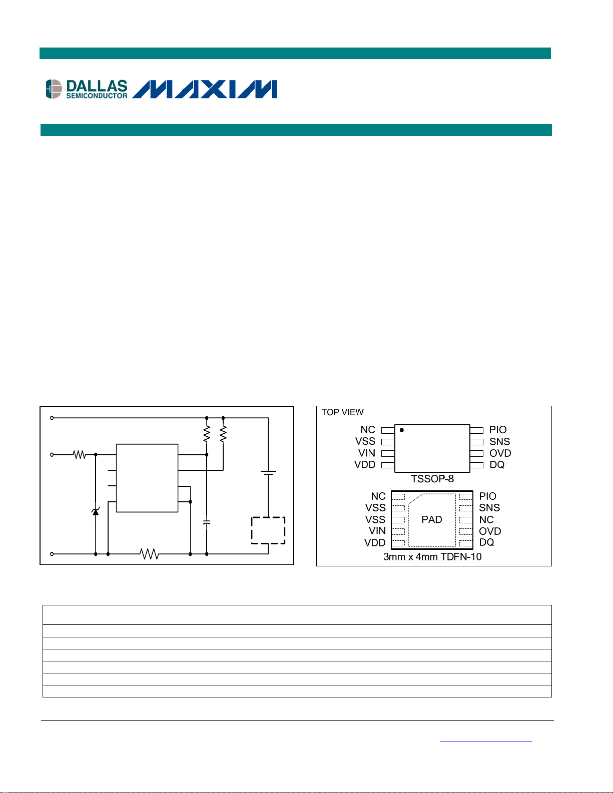
TYPICAL OPERATING CIRCUIT
PK+
DQ 5
PIO 8
NC 1
SNS 7
DS2780
4
3 VIN
6 OVD
2 VSS
TSSOP-8
RSNS
DATA
PK-
150
5.6V
500
VDD
0.1uF
1K
1 Cell
Li- Ion
Bat ter y
Protec tion
Cir c ui t
FEATURES
Precision Voltage, Temperature, and Current
Measurement System
Internal Time Base is Accurate and Temperature
Stable
Absolute and Relative Capacity Estimated from
Coulomb Count, Discharge Rate, Temperature
and Battery Cell Characteristics
Accurate Warning of Low Battery Conditions
Automatic Backup of Coulomb Count and Age
Estimation to Nonvolatile (NV) EEPROM
Gain and Tempco Calibration Allows the Use of
Low-Cost Sense Resistors
24-Byte Battery/Application Parameter EEPROM
16-Byte User EEPROM
Unique ID and Multidrop 1-Wire
®
Interface
Tiny 8-pin TSSOP & 10-pin TDFN Package
Embeds Easily in Battery Packs Using Thin
Prismatic Cells
PIN CONFIGURATION
ORDERING INFORMATION
PART MARKING PACKAGE INFORMATION
DS2780E
DS2780E/T&R 2780 TSSOP Tape-and-Reel
DS2780E+ 2780 TSSOP
DS2780E+T&R 2780 TSSOP Tape-and-Reel
DS2780G+ 2780 TDFN
DS2780G+T&R 2780 TDFN Tape-and-Reel
+Denotes lead-free package.
1-Wire is a registered trademark of Dallas Semiconductor.
Note: Some revisions of this device may incorporate deviations from published specifications known as errata. Multiple revisions of any device
may be simultaneously available through various sales channels. For information about device errata, click here: www.maxim-ic.com/errata
1 of 29
2780 TSSOP
.
REV: 050907
Page 2
DS2780 Standalone Fuel Gauge IC
ABSOLUTE MAXIMUM RATINGS
Voltage Range on Any Pin Relative to VSS -0.3V to +6.0V
Voltage on VIN Relative to VSS -0.3V to (V
+ 0.3V)
DD
Operating Temperature Range -40°C to +85°C
Storage Temperature Range
Soldering Temperature (10s)
Stresses beyond those listed under “Absolute Maximum Ratings” may cause permanent damage to the device. These are stress ratings only,
and functional operation of the device at these or any other conditions beyond those indicated in the operational sections of the specifications is
not implied. Exposure to the absolute maximum rating conditions for extended periods may affect device reliability.
-55°C to +125°C
See JEDEC J-STD-020
RECOMMENDED DC OPERATING CHARACTERISTICS
(VDD = 2.5V to 5.5V, TA = -20°C to +70°C, unless otherwise noted. Typical values are at TA = +25°C.)
PARAMETER SYMBOL CONDITIONS MIN TYP MAX UNITS
Supply Voltage VDD (Note 1) +2.5 +5.5 V
DQ, PIO, OVD Voltage
Range
DC ELECTRICAL CHARACTERISTICS
(VDD = 2.5V to 5.5V, TA = -20°C to +70°C, unless otherwise noted. Typical values are at TA = +25°C.)
PARAMETER SYMBOL CONDITIONS MIN TYP MAX UNITS
(Note 1) -0.3 +5.5 V
ACTIVE Current I
SLEEP Mode Current I
ACTIVE
SLEEP
2.5V ≤ VDD ≤ 4.2V 65 95
µA
105
2.5V ≤ VDD ≤ 4.2V 1 3 µA
Input Logic High: DQ, PIO VIH (Note 1) 1.5 V
Input Logic Low: DQ, PIO VIL (Note 1) 0.6 V
Output Logic Low: DQ, PIO VOL IOL = 4mA (Note 1) 0.4 V
Pulldown Current: DQ, PIO IPD VDQ, V
Input Logic High: OVD VIH (Note 1)
= 0.4V 0.2 µA
PIO
VDD –
0.2
V
Input Logic Low: OVD VIL (Note 1) VSS + 0.2 V
VIN Input Resistance RIN 15
MΩ
DQ Capacitance CDQ 50 pF
DQ SLEEP Timeout t
Undervoltage SLEEP
Threshold
DQ < VIL (Note 5) 1.5 2.0 2.5 s
SLEEP
V
(Note 1) 2.40 2.45 2.50 V
SLEEP
ELECTRICAL CHARACTERISTICS: TEMPERATURE, VOLTAGE, CURRENT
(VCC = 2.5V to 5.5V, TA = -20°C to +70°C, unless otherwise noted. Typical values are at TA = +25°C.)
PARAMETER SYMBOL CONDITIONS MIN TYP MAX UNITS
Temperature Resolution T
Temperature Error T
Voltage Resolution V
Voltage Full-Scale VFS 0 4.992 V
0.125 °C
LSB
±3 °C
ERR
4.88 mV
LSB
Voltage Error V
Current Resolution I
±50 mV
ERR
1.56 µV
LSB
Current Full-Scale IFS ±51.2 mV
2 of 29
Page 3

DS2780 Standalone Fuel Gauge IC
PARAMETER SYMBOL CONDITIONS MIN TYP MAX UNITS
Current Gain Error I
Current Offset Error I
(Note 2) ±1
GERR
≤ +70°C,
A
- 7.82 + 12.5 µV
OERR
0°C ≤ T
2.5V ≤ VDD ≤ 4.2V
(Note 4)
Accumulated Current Offset q
OERR
0°C ≤ T
2.5V ≤ VDD ≤ 4.2V
VSNS = VSS, (Notes 3,
≤ +70°C,
A
- 188 + 0
4)
VDD = 3.8V, TA = +25°C ±1
Timebase Error t
ERR
0°C ≤ TA ≤ +70°C,
2.5V ≤ VDD ≤ 4.2V
±2
±3
ELECTRICAL CHARACTERISTICS: 1-WIRE INTERFACE, STANDARD
(VCC = 2.5V to 5.5V, TA = -20°C to +70°C.)
PARAMETER SYMBOL CONDITIONS MIN TYP MAX UNITS
% Full-
Scale
µVhr/
day
%
Time Slot t
Recovery Time t
Write-0 Low Time t
Write-1 Low Time t
Read Data Valid t
Reset Time High t
Reset Time Low t
Presence Detect High t
Presence Detect Low t
60 120
SLOT
1
REC
60 120
LOW0
1 15
LOW1
15
RDV
480
RSTH
480 960
RSTL
15 60
PDH
60 240
PDL
ELECTRICAL CHARACTERISTICS: 1-WIRE INTERFACE, OVERDRIVE
(VCC = 2.5V to 5.5V, TA = -20°C to +70°C.)
PARAMETER SYMBOL CONDITIONS MIN TYP MAX UNITS
Time Slot t
Recovery Time t
Write-0 Low Time t
Write-1 Low Time t
Read Data Valid t
Reset-Time High t
Reset-Time Low t
Presence-Detect High t
Presence-Detect Low t
6 16
SLOT
1
REC
6 16
LOW0
1 2
LOW1
2
RDV
48
RSTH
48 80
RSTL
2 6
PDH
8 24
PDL
μs
μs
μs
μs
μs
μs
μs
μs
μs
μs
μs
μs
μs
μs
μs
μs
μs
μs
3 of 29
Page 4

DS2780 Standalone Fuel Gauge IC
EEPROM RELIABILITY SPECIFICATION
(VCC = 2.5V to 5.5V, TA = -20°C to +70°C, unless otherwise noted. Typical values are at TA = +25°C.)
PARAMETER SYMBOL CONDITIONS MIN TYP MAX UNITS
EEPROM Copy Time t
EEPROM Copy Endurance N
10 ms
EEC
TA = +50°C 50,000 cycles
EEC
Note 1: All voltages are referenced to VSS.
Note 2: Factory calibrated accuracy. Higher accuracy can be achieved by in-system calibration by the user.
Note 3: Accumulation bias register set to 00h.
Note 4: Parameters guaranteed by design.
Note 5: The application must wait for the maximum DQ SLEEP Timeout to confirm that the IC has entered sleep
mode.
PIN DESCRIPTION
NAME
TSSOP
PIN
NC 1 1 Not Connected. Pin not connected internally, float or connect to VSS.
VSS 2 2, 3
VIN 3 4
VDD 4 5
DQ 5 6
OVD 6 7
TDFN
PIN
FUNCTION
Device Ground. Connect directly to the negative terminal of the battery cell. Connect
the sense resistor between VSS and SNS.
Voltage Sense Input. The voltage of the battery cell is monitored through this input
pin.
Power-Supply Input. Connect to the positive terminal of the battery cell through a
decoupling network.
Data Input/Output. 1-Wire data line. Open-drain output driver. Connect this pin to the
DATA terminal of the battery pack. This pin has a weak internal pulldown (IPD) for
sensing pack disconnection from host or charger.
1-Wire Bus Speed Control.
Input logic level selects the speed of the 1-Wire bus.
Logic 1 selects overdrive (OVD) and Logic 0 selects standard timing (STD). On a
multidrop bus, all devices must operate at the same speed.
NC — 8 Not Connected. Pin not connected internally, float or connect to VSS.
SNS 7 9
Sense Resistor Connection. Connect to the negative terminal of the battery pack.
Connect the sense resistor between VSS and SNS.
Programmable I/O Pin. Can be configured as input or output to monitor or control
PIO 8 10
user-defined external circuitry. Output driver is open drain. This pin has an weak
internal pulldown (I
PD
).
PAD — PAD Exposed Pad. Connect to VSS or leave floating. (Only present on TDFN package)
4 of 29
Page 5
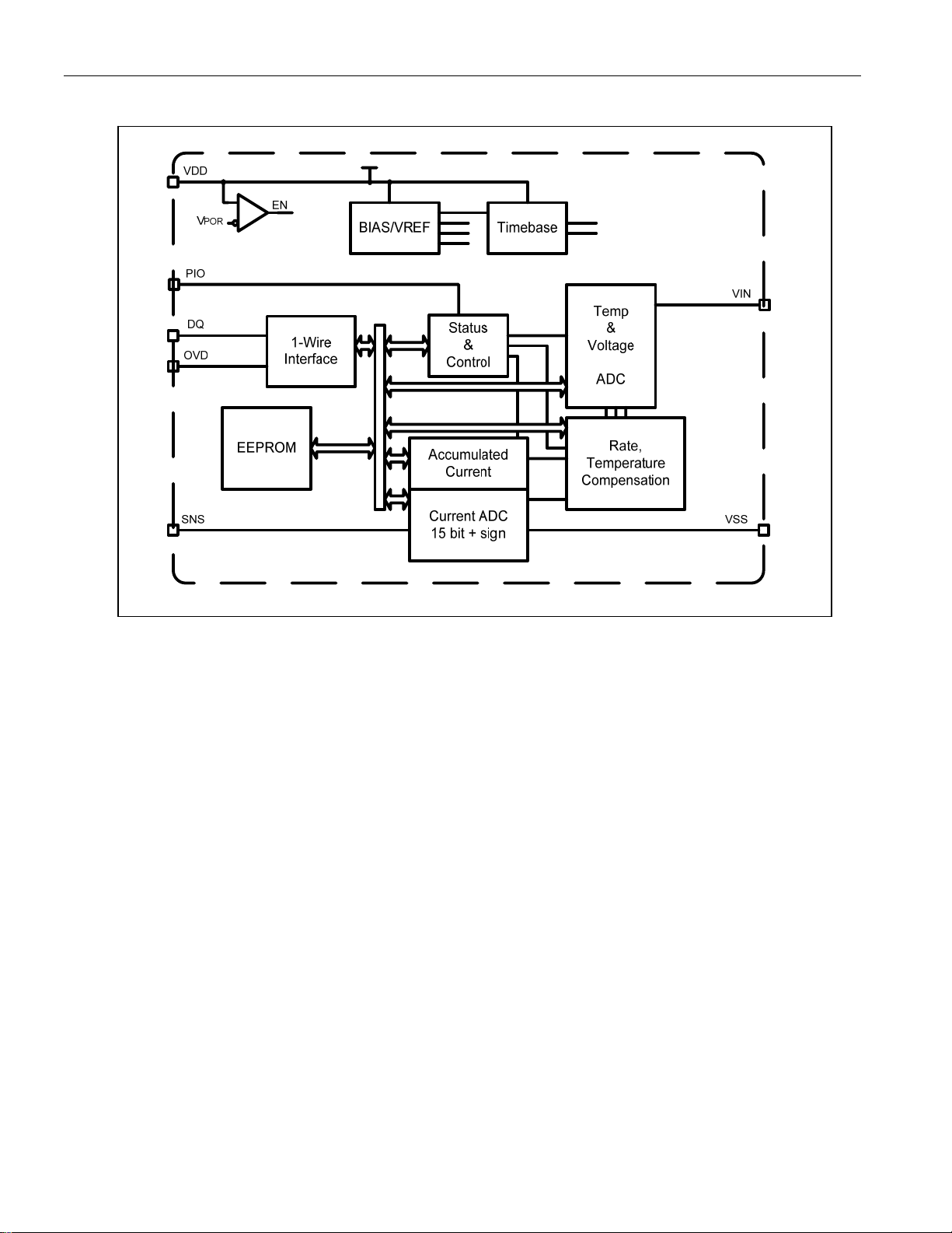
Figure 1. Block Diagram
DS2780 Standalone Fuel Gauge IC
DETAILED DESCRIPTION
The DS2780 operates directly from 2.5V to 5.5V and supports single cell Lithium-ion battery packs. As shown in
Figure 2, the DS2780 accommodates multicell applications by adding a voltage regulator for VDD and voltage
divider for VIN. Nonvolatile storage is provided for cell compensation and application parameters. Host side
development of fuel-gauging algorithms is eliminated. On-chip algorithms and convenient status reporting of
operating conditions reduce the serial polling required of the host processor. For 2-cell applications, the DS2781 is
recommended, since it includes a voltage regulator and accepts VIN up to 10V.
Additionally, 16 bytes of EEPROM memory are made available for the exclusive use of the host system and/or
pack manufacturer. The additional EEPROM memory can be used to facilitate battery lot and date tracking and
non-volatile storage of system or battery usage statistics.
A Dallas 1-Wire interface provides serial communication at the standard 16kbps or overdrive 140kbps speeds. It
allows access to data registers, control registers and user memory. A unique, factory programmed 64-bit
registration number (8-bit family code + 48-bit serial number + 8-bit CRC) assures that no two parts are alike and
enables absolute traceability. The Dallas 1-Wire interface on the DS2780 supports multidrop capability so that
multiple slave devices may be addressed with a single pin.
5 of 29
Page 6
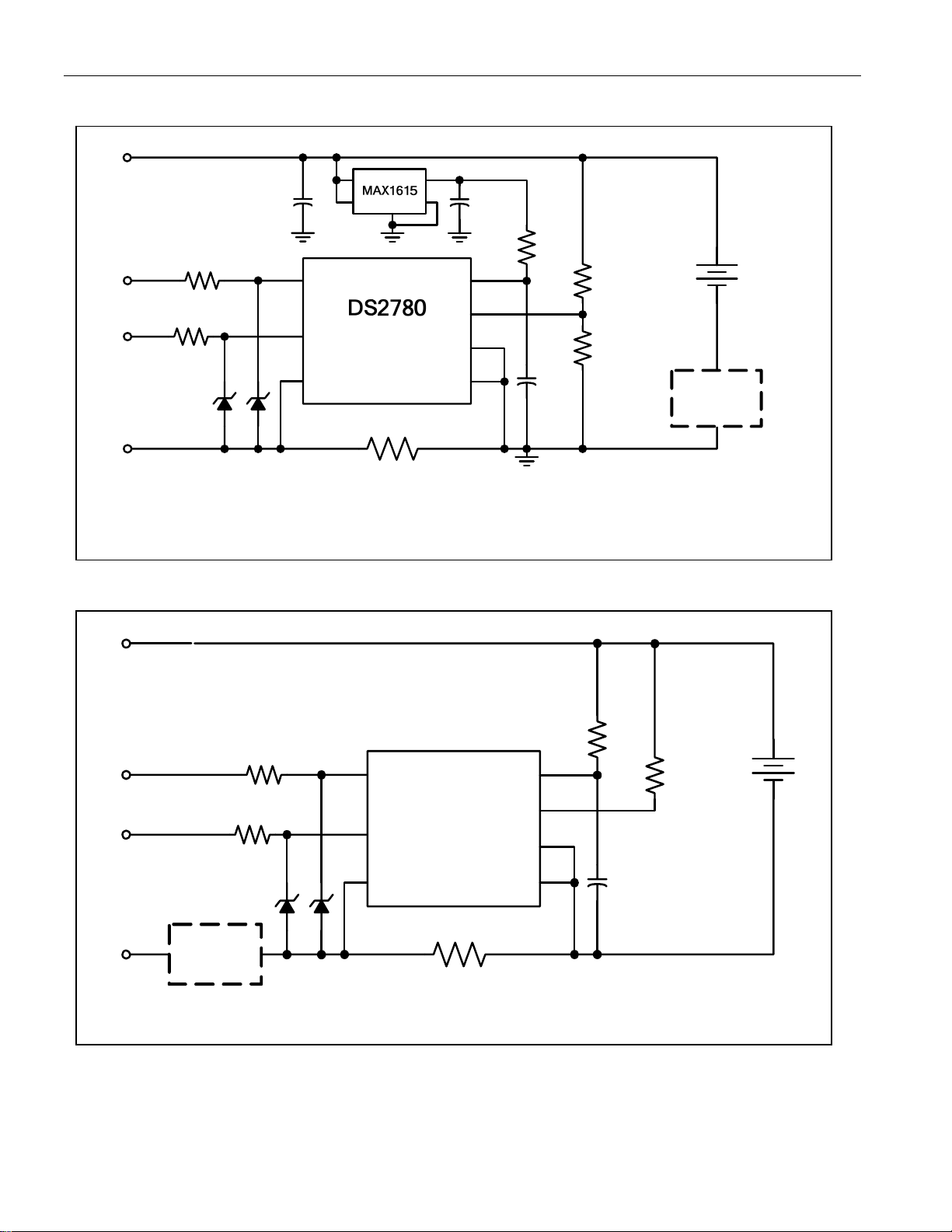
Figure 2. Multicell Application Example
PK+
DS2780 Standalone Fuel Gauge IC
4.7uF0.1uF
DATA
PIO
PK-
150
DQ
150
PIO
(1) (1)
(1) Components improve IEC1004 Air/Contact ESD compliance
SNS
RSNS
VDD
VIN
OVD
VSS
500
0.1uF
(n * R)
R
Multi-Cell
Li-Ion
Battery
Protection
Circuit
Figure 3. Inside Protector Example
PK+
DATA
PIO
150
150
DQ
PIO
DS2780
VDD
VIN
OVD
500
1K
Li-Ion
Battery
(1) (1)
PK-
Protection
Circuit
SNS
VSS
0.1uF
RSNS
(1) Precaution must be taken to ensure that a charge path is not created from
PK+ to Data or PIO.
PROTECTOR CIRCUIT LOCATION
The battery protection circuitry can be located inside or outside the DS2780. Either location is acceptable but there
are some advantages and disadvantages to both. With the protection circuit located inside, see Figure 2 and
Typical Operating Circuit on page 1, the DS2780 will loose power in a circuit protection event. The DS2780 stores
fuel gauge data to EEPROM, but some data loss can occur depending on the timing of the protection event and the
6 of 29
Page 7
DS2780 Standalone Fuel Gauge IC
backup. When the protection circuit is connected directly to the battery the protection is absolute, no charging will
occur during a protection event. With the protection circuit located outside, see Figure 3, the DS2780 will remain
powered up during a protection event. The disadvantage to this configuration is that you run the risk of
overcharging the battery by creating an unintentional charge path from PK+ to DATA or PIO (V
PK+
> V
CELL
+ V
DIODE
).
Communication to the DS2780 is broken during a protection event regardless of protector location.
POWER MODES
The DS2780 has two power modes: ACTIVE and SLEEP. On initial power up, the DS2780 defaults to ACTIVE
mode. While in ACTIVE mode, the DS2780 is fully functional with measurements and capacity estimation
continuously updated. In SLEEP mode, the DS2780 conserves power by disabling measurement and capacity
estimation functions, but preserves register contents. SLEEP mode is entered under two different conditions and
an enable bit for each condition makes entry into SLEEP optional. SLEEP mode can be enabled using the Power
Mode (PMOD) bit or the Under Voltage Enable (UVEN) bit.
The PMOD type SLEEP is entered if the PMOD bit is set AND DQ is low for t
DQ low for t
can be used to detect a pack disconnection or system shutdown, in which no charge or discharge
SLEEP
(2s nominal). The condition of
SLEEP
current will flow. A PMOD SLEEP condition transitions back to ACTIVE mode when DQ is pulled high.
The second option for entering SLEEP is an under voltage condition. When the UVEN bit is set, the DS2780
transitions to SLEEP if the voltage on VIN is less than V
logic level for t
. An under-voltage condition occurs when a pack is fully discharged, where loading on the
SLEEP
battery should be minimized. UVEN type SLEEP relieves the battery of the I
(2.45V nominal) AND DQ is stable at a low or high
SLEEP
load until communication on DQ
ACTIVE
resumes.
NOTE: PMOD and UVEN SLEEP features must be disabled when a battery is charged on an external charger that
does not connect to the DQ pin. PMOD SLEEP can be used if the charger pulls DQ high. UVEN SLEEP can be
used if the charger toggles DQ. The DS2780 remains in SLEEP on a charger that fails to properly drive DQ and
therefore does not measure or accumulate current when a battery is charged.
INITIATING COMMUNICATION IN SLEEP
When beginning communication with a DS2780 in PMOD SLEEP, DQ must be pulled up first and then a 1-Wire
Reset pulse must be issued by the master. In UVEN SLEEP, the procedure depends on the state of DQ when
UVEN SLEEP was entered. If DQ was low, DQ must be pulled up and then a 1-Wire Reset pulse must be issued
by the master as with PMOD SLEEP. If DQ was high when UVEN SLEEP was entered, then the DS2780 is
prepared to receive a 1-Wire reset from the master. In the first two cases with DQ low during SLEEP, the DS2780
does not respond to the first rising edge of DQ with a presence pulse.
VOLTAGE MEASUREMENT
Battery voltage is measured at the VIN input with respect to VSS. It has a range of 0V to 4.992V and a resolution
of 4.88mV. The measurement is stored in the VOLTAGE register in two’s compliment form and is updated every
440ms. Voltages above the maximum register value are reported at the maximum value; voltages below the
minimum register value are reported at the minimum value. The format of the voltage register is shown in Figure 4.
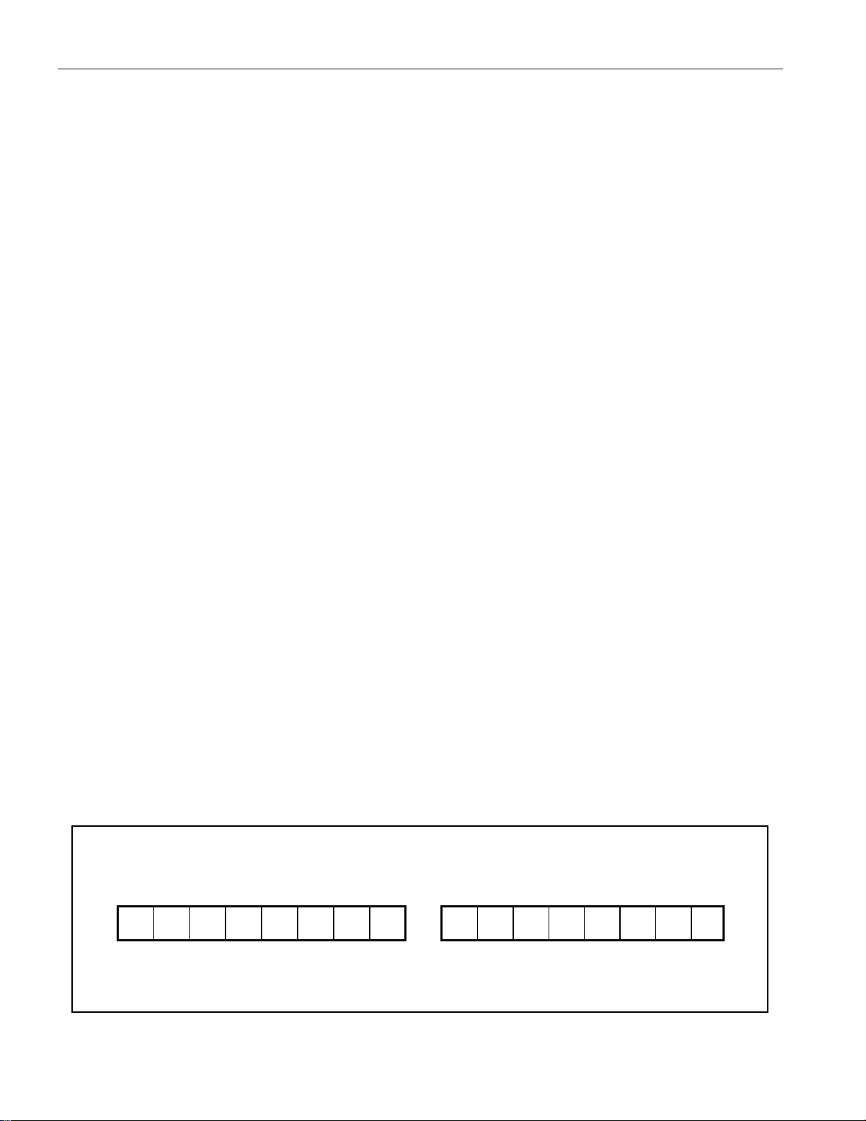
Figure 4. Voltage Register Format
VOLT
Read Only
MSB—Address 0Ch LSB—Address 0Dh
9
S 2
28 27 26 25 24 23 22 21 20 X X X X X
MSb LSb MSb LSb
“S”: sign bit(s), “X”: reserved
Units: 4.88mV
7 of 29
Page 8
DS2780 Standalone Fuel Gauge IC
VIN is usually connected to the positive terminal of a single cell Lithium-Ion battery via a 1kΩ resistor. The input
impedance is large enough (15MΩ) to be connected to a high impedance voltage divider in order to support
multiple cell applications. The pack voltage should be divided by the number of series cells to present a single cell
average voltage to the VIN input. In Figure 2, the value of R can be up to 1MΩ without incurring significant error
due to input loading.
TEMPERATURE MEASUREMENT
The DS2780 uses an integrated temperature sensor to measure battery temperature with a resolution of 0.125°C.
Temperature measurements are updated every 440ms and placed in the temperature register in two’s complement
form. The format of the temperature register is shown in Figure 5.
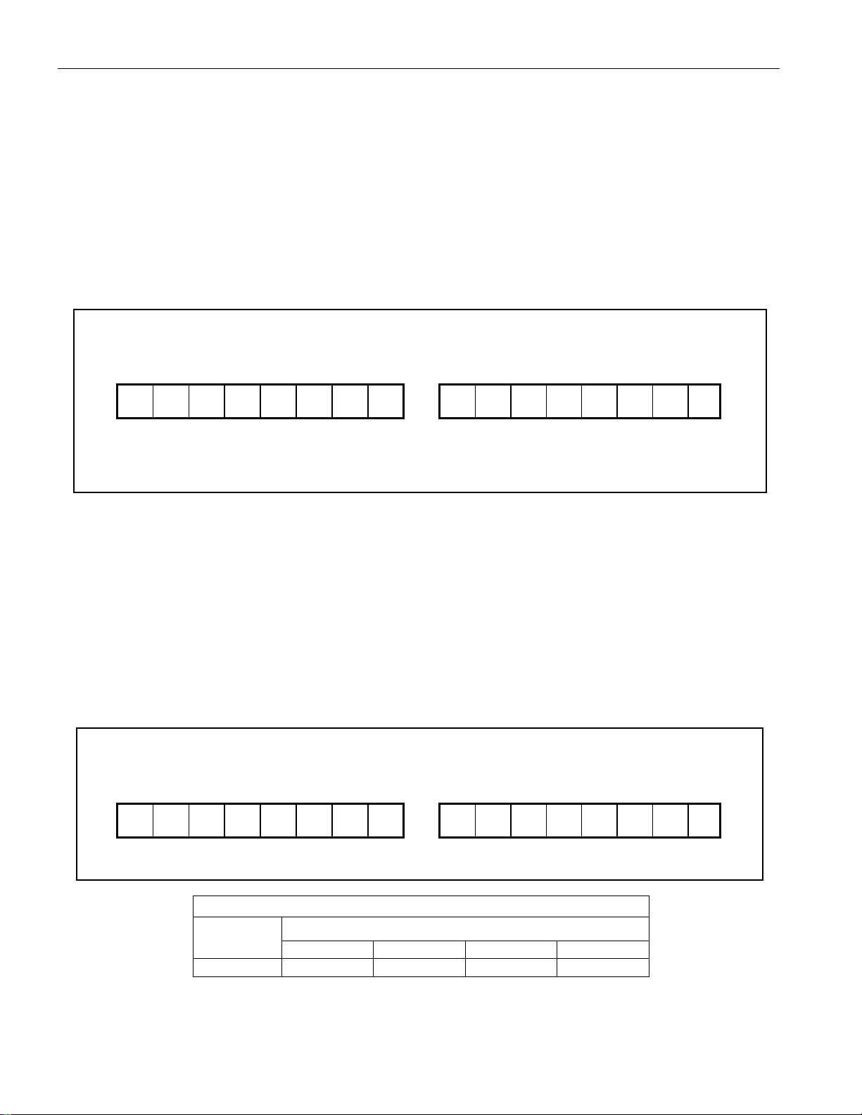
Figure 5. Temperature Register Format
TEMP
Read Only
MSB—Address 0Ah LSB—Address 0Bh
9
S 2
28 27 26 25 24 23 22 21 20 X X X X X
MSb LSb MSb LSb
“S”: sign bit(s), “X”: reserved
Units: 0.125°C
CURRENT MEASUREMENT
In the ACTIVE mode of operation, the DS2780 continually measures the current flow into and out of the battery by
measuring the voltage drop across a low-value current-sense resistor, R
. The voltage-sense range between
SNS
SNS and VSS is ±51.2mV. The input linearly converts peak signal amplitudes up to 102.4mV as long as the
continuous signal level (average over the conversion cycle period) does not exceed ±51.2mV. The ADC samples
the input differentially at 18.6kHz and updates the Current register at the completion of each conversion cycle.
The Current register is updated every 3.515s with the current conversion result in two’s complement form. Charge
currents above the maximum register value are reported at the maximum value (7FFFh = +51.2mV). Discharge
currents below the minimum register value are reported at the minimum value (8000h = -51.2mV).
Figure 6. Current Register Format
CURRENT
S 2
MSB—Address 0Eh LSB—Address 0Fh
14
213 212 211 210 29 28 27 26 25 24 23 22 21 20
MSb LSb MSb LSb
“S”: sign bit(s)
CURRENT RESOLUTION (1 LSB)
VSS VSNS
20mΩ 15mΩ 10mΩ 5mΩ
1.5625μV 78.13μA 104.2μA 156.3μA 312.5μA
AVERAGE CURRENT MEASUREMENT
Units: 1.5625μV/Rsns
R
SNS
8 of 29
Read Only
Page 9
DS2780 Standalone Fuel Gauge IC
The Average Current register reports an average current level over the preceding 28 seconds. The register value is
updated every 28s in two’s complement form, and is the average of the 8 preceding Current register updates. The
format of the Average Current register is shown in Figure 7. Charge currents above the maximum register value
are reported at the maximum value (7FFFh = +51.2mV). Discharge currents below the minimum register value are
reported at the minimum value (8000h = -51.2mV).
Figure 7. Average Current Register Format
IAVG
S 2
MSb LSb MSb LSb
“S”: sign bit(s)
MSB—Address 08h LSB—Address 09h
14
213 212 211 210 29 28 27 26 25 24 23 22 21 20
Units: 1.5625μV/Rsns
Read Only
CURRENT OFFSET CORRECTION
Every 1024th conversion, the ADC measures its input offset to facilitate offset correction. Offset correction occurs
approximately once per hour. The resulting correction factor is applied to the subsequent 1023 measurements.
During the offset correction conversion, the ADC does not measure the sense resistor signal. A maximum error of
1/1024 in the accumulated current register (ACR) is possible; however, to reduce the error, the current
measurement made just prior to the offset conversion is displayed in the current register and is substituted for the
dropped current measurement in the current accumulation process. This results in an accumulated current error
due to offset correction of less than 1/1024.
CURRENT MEASUREMENT CALIBRATION
The DS2780’s current measurement gain can be adjusted through the RSGAIN register, which is factory-calibrated
to meet the data sheet specified accuracy. RSGAIN is user accessible and can be reprogrammed after module or
pack manufacture to improve the current measurement accuracy. Adjusting RSGAIN can correct for variation in an
external sense resistor’s nominal value, and allows the use of low-cost, non-precision current sense resistors.
RSGAIN is an 11 bit value stored in 2 bytes of the Parameter EEPROM Memory Block. The RSGAIN value adjusts
the gain from 0 to 1.999 in steps of 0.001 (precisely 2
accurate current measurement. When shipped from the factory, the gain calibration value is stored in two separate
locations in the Parameter EEPROM Block, RSGAIN which is reprogrammable and FRSGAIN which is read only.
RSGAIN determines the gain used in the current measurement. The read-only FRSGAIN is provided to preserve
the factory value only and is not used in the current measurement.
-10
). The user must program RSGAIN cautiously to ensure
SENSE RESISTOR TEMPERATURE COMPENSATION
The DS2780 is capable of temperature compensating the current sense resistor to correct for variation in a sense
resistor’s value over temperature. The DS2780 is factory programmed with the sense resistor temperature
coefficient, RSTC, set to zero, which turns off the temperature compensation function. RSTC is user accessible
and can be reprogrammed after module or pack manufacture to improve the current accuracy when using a high
temperature coefficient current-sense resistor. RSTC is an 8-bit value stored in the Parameter EEPROM Memory
Block. The RSTC value sets the temperature coefficient from 0 to +7782ppm/ºC in steps of 30.5ppm/ºC. The user
must program RSTC cautiously to ensure accurate current measurement.
Temperature compensation adjustments are made when the Temperature register crosses 0.5
temperature compensation is most effective with the resistor placed as close as possible to the VSS terminal. This
will optimize thermal coupling of the resistor to the on-chip temperature sensor. The current shunt trace should be
run under the DS2780 package, and it should be constructed with a copper PCB trace.
o
C boundaries. The
CURRENT ACCUMULATION
Current measurements are internally summed, or accumulated, at the completion of each conversion period and
the results are stored in the Accumulated Current Register (ACR). The accuracy of the ACR is dependent on the
current measurement and the conversion timebase. The ACR has a range of 0 to 409.6mVh with an LSb of
6.25μVh. Additional read-only registers (ACRL) hold fractional results of each accumulation to avoid truncation
9 of 29
Page 10

DS2780 Standalone Fuel Gauge IC
errors. Accumulation of charge current above the maximum register value is reported at the maximum register
value (7FFFh); conversely, accumulation of discharge current below the minimum register value is reported at the
minimum value (8000h).
Charge currents (positive Current register values) less than 100μV are not accumulated in order to mask the effect
of accumulating small positive offset errors over long periods. This limits the minimum charge current, for coulombcounting purposes, to 5mA for RSNS = 0.020Ω and 20mA for RSNS = 0.005Ω.
Read and write access is allowed to the ACR. The ACR must be written MSByte first then LSByte. The write must
be completed within 3.515s (one ACR register update period). A write to the ACR forces the ADC to perform an
offset correction conversion and update the internal offset correction factor. Current measurement and
accumulation begins with the second conversion following a write to the ACR. Writing the ACR clears the fractional
values in the ACRL. The format of the ACR is shown in Figure 8, and the ACRL is shown in Figure 9.
To preserve the ACR value in case of power loss, it is backed up to EEPROM. The ACR value is recovered from
EEPROM on power-up. See the Memory Map in Table 2 for specific address location and backup frequency.
Figure 8. Accumulated Current Register Format, ACR
ACR
MSB—Address 10h LSB—Address 11h
15
2
214 213 212 211 210 29 28 27 26 25 24 23 22 21 20
MSb LSb MSb LSb
Units: 6.25μVh/Rsns
Figure 9. Fractional/Low Accumulated Current Register Format, ACRL
ACRL
MSB—Address 12h LSB—Address 13h
11
2
210 29 28 27 26 25 24 23 22 21 20 X X X X
MSb LSb MSb LSb
“X”: reserved Units:1.526nVHr/R
ACR LSb
R
VSS VSNS
20mΩ 15mΩ 10mΩ 5mΩ
SNS
R/W & EE
Read Only
SNS
6.25μVh 312.5μAh 416.7μAh 625μAh
1.250mAh
10 of 29
Page 11

DS2780 Standalone Fuel Gauge IC
ACR RANGE
R
VSS VSNS
±409.6mVh ±20.48Ah ±27.30Ah ±40.96Ah ±81.92Ah
20mΩ 15mΩ 10mΩ 5mΩ
SNS
ACCUMULATION BIAS
The Accumulation Bias register (AB) allows an arbitrary bias to be introduced into the current-accumulation
process. The AB can be used to account for currents that do not flow through the sense resistor, estimate currents
too small to measure, estimate battery self-discharge or correct for static offset of the DS2780. The AB register
allows a user programmed constant positive or negative polarity bias to be included in the current accumulation
process. The user-programmed two’s compliment value, with bit weighting the same as the current register, is
added to the ACR once per current conversion cycle. The AB value is loaded on power-up from EEPROM. The
format of the AB register is shown in Figure 10.
Figure 10. Accumulation Bias Register Formats
AB
Address 61h
EE
S 26 25 24 23 22 21 20
MSb LSb
“S”: sign bit Units: 1.5625μV/Rsns
CAPACITY ESTIMATION ALGORITHM
Remaining capacity estimation uses real-time measured values, stored parameters describing the cell
characteristics, and application operating limits. The following diagram describes the algorithm inputs and outputs.
11 of 29
Page 12
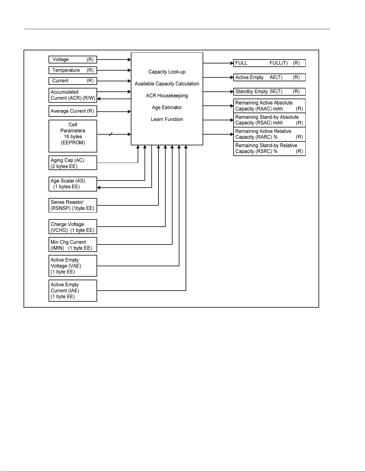
Figure 11. Top Level Algorithm Diagram
DS2780 Standalone Fuel Gauge IC
MODELING CELL CHARACTERISTICS
In order to achieve reasonable accuracy in estimating remaining capacity, the cell performance characteristics over
temperature, load current, and charge termination point must be considered. Since the behavior of Li-ion cells is
non-linear, even over a limited temperature range of 10°C to 35°C, these characteristics must be included in the
capacity estimation to achieve a reasonable accuracy. See Applications Note AN131 “Li+ Fuel Gauging with Dallas
Semiconductor Devices” for general information on the FuelPack™ method used in the DS2780. To facilitate
efficient implementation in hardware, a modified version of the method outlined in AN131 is used to store cell
characteristics in the DS2780. Full and empty points are retrieved in a lookup process which re-traces a piece-wise
linear model. Three model curves are stored: Full, Active Empty and Standby Empty. Each model curve is
constructed with 4 line segments and spans from 0°C to 40°C. Operation outside the 0°C to 40°C model span is
supported by the model with minimal loss of accuracy. Above 40°C, the 40°C fixed points are extended with zero
slope. This achieves a conservative capacity estimate for temperatures above 40°C. Below 0°C, the model curves
are extended using the slope of each 0°C to 10°C segment. If low temperature operation is expected, the 0°C to
10°C slopes can be selected to optimize the model accuracy. A diagram of example battery cell model curves is
shown in Figure 12.
FuelPack is a trademark of Dallas Semiconductor.
12 of 29
Page 13

Figure 12. Cell Model Example Diagram
pty
pty
100%
DS2780 Standalone Fuel Gauge IC
Derivative
[ppm / °C]
FULL
Cell
Characterization
Active
data points
Em
Standby
Em
1
0°C 10°C 20°C 30°C 40°C
2
3
4
Full: The Full curve defines how the full point of a given cell depends on temperature for a given charge
termination. The application’s charge termination method should be used to determine the table values. The
DS2780 reconstructs the Full line from the cell characteristic table to determine the Full capacity of the battery at
each temperature. Reconstruction occurs in one-degree temperature increments.
Active Empty: The Active Empty curve defines the variation of the Active Empty Point over temperature. The
Active Empty Point is defined as the minimum voltage required for system operation at a discharge rate based on a
high level load current (one that is sustained during a high power operating mode). This load current is
programmed as the Active Empty current (IAE) and should be a 3.5s average to correspond to values read from
the Current register. The specified minimum voltage, or Active Empty voltage (VAE), should be a 220ms average
to correspond to values read from the Voltage register. The DS2780 reconstructs the Active Empty line from the
cell characteristic table to determine the Active Empty capacity of the battery at each temperature. Reconstruction
occurs in one-degree temperature increments.
Standby Empty: The Standby Empty curve defines the variation of the standby empty point over temperature.
The standby empty point is defined as the minimum voltage required for standby operation at a discharge rate
dictated by the application standby current. In typical PDA applications, Standby Empty represents the point that
the battery can no longer support RAM refresh and thus the standby voltage is set by the RAM voltage supply
requirements. In other applications, Standby Empty can represent the point that the battery can no longer support a
subset of the full application operation, such as games or organizer functions on a wireless handset. The standby
load current and voltage are used for determining the cell characteristics but are not programmed into the DS2780.
The DS2780 reconstructs the Standby Empty line from the cell characteristic table to determine the Standby Empty
capacity of the battery at each temperature. Reconstruction occurs in one-degree temperature increments.
13 of 29
Page 14

DS2780 Standalone Fuel Gauge IC
CELL MODEL CONSTRUCTION
The model is constructed with all points normalized to the fully charged state at +40°C. All values are stored in the
cell parameter EEPROM block. The +40°C Full value is stored in uVhr with an LSB of 6.25uVhr. The +40°C Active
Empty value is stored as a percentage of +40°C Full with a resolution of 2
definition zero and therefore no storage is required. The slopes (derivatives) of the 4 segments for each model
curve are stored in the cell parameter EEPROM block as PPM/°C. Segment endpoints are fixed at 0°C, +10°C,
+20°C, +30°C and +40°C. (See Application Note 3584 for more details on how values are stored.) An example of
cell model data is shown in Table 1a. Table 1b shows the actual data values stored in memory.
-10
. Standby Empty at +40°C is by
Table 1a. Example Cell Characterization Table (Normalized to +40°C)
Rated cell capacity: 1000mAh
Charge Voltage: 4.2V Terminating Current: 50mA
Active Empty (V): 3.0V Active Empty (I): 300mA
Sense Resistor: 0.020Ω
Full 1051 0.927 0.951 0.974 0.991 1.0
Active Empty 0.051 0.040 0.022 0.012 0.008
Standby Empty 0.013 0.0067 0.0038 0.001 0
+40°C
Nominal
[mAh]
0°C +10°C +20°C +30°C +40°C
Table 1b. Example Cell Characterization Table (Actual data values stored in EEPROM)
Rated cell capacity: 0C80h
Charge Voltage: D7h Terminating Current: 14h
Active Empty (V): 9Ah Active Empty (I): 1Eh
Sense Resistor: 32h
Full 0D32h 27h 26h 1Ch 0Fh 0D32h
Active Empty 12h 1Eh 10h 07h 08h
Standby Empty 0Ah 05h 05h 02h
+40°C
Nominal
[mAh]
0°C +10°C +20°C +30°C +40°C
Figure 13. Lookup Function Diagram
Cell Model
Parameters
15 bytes
(EEPROM)
Temperature
Lookup
Function
FULL(T)
AE(T)
SE(T)
APPLICATION PARAMETERS
In addition to cell model characteristics, several application parameters are needed to detect the full and empty
points, as well as calculate results in mAh units.
14 of 29
Page 15

DS2780 Standalone Fuel Gauge IC
Sense Resistor Prime (RSNSP[1/Ω]): RSNSP stores the value of the sense resistor for use in computing the
absolute capacity results. The resistance is stored as a 1-byte conductance value with units of mhos (1/Ω). RSNSP
supports resistor values of 1Ω to 3.922mΩ. RSNSP is located in the Parameter EEPROM block.
RSNSP = 1/RSNS (units of mhos; 1/Ω)
Charge Voltage (VCHG): VCHG stores the charge voltage threshold used to detect a fully charged state. The
voltage is stored as a 1-byte value with units of 19.52mV and can range from 0V to 4.978V. VCHG should be set
marginally less than the cell voltage at the end of the charge cycle to ensure reliable charge termination detection.
VCHG is located in the Parameter EEPROM block.
Minimum Charge Current (IMIN): IMIN stores the charge current threshold used to detect a fully charged state. It
is stored as a 1-byte value with units of 50μV (IMIN * RSNS) and can range from 0 to 12.75mV. Assuming RSNS =
20mΩ, IMIN can be programmed from 0mA to 637.5mA in 2.5mA steps. IMIN should be set marginally greater than
the charge current at the end of the charge cycle to ensure reliable charge termination detection. IMIN is located in
the Parameter EEPROM block.
Active Empty Voltage (VAE): VAE stores the voltage threshold used to detect the Active Empty Point. The value
is stored in 1-byte with units of 19.52mV and can range from 0V to 4.978V. VAE is located in the Parameter
EEPROM block. See the Cell Characteristics section for more information.
Active Empty Current (IAE): IAE stores the discharge current threshold used to detect the Active Empty Point.
The unsigned value represents the magnitude of the discharge current and is stored in 1-byte with units of 200μV.
It can range from 0 to 51.2mV. Assuming RSNS = 20mΩ, IAE can be programmed from 0mA to 2550mA in 10mA
steps. IAE is located in the Parameter EEPROM block. See the Cell Characteristics section for more information.
Aging Capacity (AC): AC stores the rated cell capacity which is used to estimate the decrease in battery capacity
that occurs during normal use. The value is stored in 2-bytes in the same units as the ACR (6.25μVh). When set to
the manufacturer’s rated cell capacity the Aging Estimation rate is approximately 2.4% per 100 cycles of equivalent
full capacity discharges. Partial discharge cycles are added to form equivalent full capacity discharges. The default
aging estimation results in 88% capacity after 500 equivalent cycles. The Aging Estimation rate can be adjusted by
setting the AC to a value other than the cell manufacturer’s rating. Setting AC to a lower value, accelerates the
Aging Estimation rate. Setting the AC to a higher value, retards the Aging Estimation rate. The AC is located in the
Parameter EEPROM block.
Age Scalar (AS): AS adjusts the cell capacity estimation results downward to compensate for aging. The AS is a
1-byte value that has a range of 49.2% to 100%. The lsb is weighted at 0.78% (precisely 2
-7
). A value of 100% (128
decimal or 80h) represents an un-aged battery. A value of 95% is recommended as the starting AS value at the
time of pack manufacture to allow the learning of a larger capacity on batteries that have an initial capacity greater
than the rated cell capacity programmed in the cell characteristic table. The AS is modified by the Aging Estimation
introduced under Aging Capacity and by the Learn function. The host system has read and write access to the AS,
however caution should be exercised when writing it to ensure that the cumulative aging estimate is not over
written with an incorrect value. Usually, writing the AS by the host is not necessary because it is automatically
saved to EEPROM on a periodic basis by the DS2780. (See the Memory section for details.) The AS value stored
in EEPROM is recalled on power-up.
CAPACITY ESTIMATION UTILITY FUNCTIONS
Aging Estimation
As discussed above, the AS register value is adjusted occasionally based on cumulative discharge. As the ACR
register decrements during each discharge cycle, an internal counter is incremented until equal to 32 times the AC.
The AS is then decremented by one, resulting in a decrease in the scaled full battery capacity of 0.78%
(approximately 2.4% per 100 cycles). Refer to the AC register description above for recommendations on
customizing the age estimation rate.
Learn Function
Since Li+ cells exhibit charge efficiencies near unity, the charge delivered to a Li+ cell from a known empty point to
a known full point is a dependable measure of the cell capacity. A continuous charge from empty to full results in a
15 of 29
Page 16

DS2780 Standalone Fuel Gauge IC
“learn cycle”. First, the Active Empty Point must be detected. The Learn Flag (LEARNF) is set at this point. Then,
once charging starts, the charge must continue uninterrupted until the battery is charged to full. Upon detecting full,
LEARNF is cleared, the Charge to Full (CHGTF) flag is set and the Age Scalar (AS) is adjusted according to the
learned capacity of the cell.
ACR Housekeeping
The ACR value is adjusted occasionally to maintain the coulomb count within the model curve boundaries. When
the battery is charged to full (CHGTF set), the ACR is set equal to the age scaled full lookup value at the present
temperature. If a learn cycle is in progress, correction of the ACR value occurs after the age scalar (AS) is updated.
When an empty condition is detected (AEF or LEARNF set), the ACR adjustment is conditional. If AEF is set and
LEARNF is not, then the Active Empty Point was not detected and the battery is likely below the Active Empty
capacity of the model. The ACR is set to the Active Empty model value only if it is greater than the Active Empty
model value. If LEARNF is set, then the battery is at the Active Empty Point and the ACR is set to the Active Empty
model value.
Full Detect
Full detection occurs when the Voltage (VOLT) readings remain above the VCHG (Charge Voltage) threshold for
the duration of two Average Current (IAVG) readings, where both IAVG readings are below IMIN (Terminating
Current). The two consecutive IAVG readings must also be positive and non-zero. This ensures that removing the
battery from the charger does not result in a false detection of full. Full Detect sets the Charge to Full (CHGTF) bit
in the Status register.
Active Empty Point Detect
Active Empty Point detection occurs when the Voltage register drops below the VAE threshold and the two
previous Current readings are above IAE. This captures the event of the battery reaching the Active Empty Point.
Note that the two previous Current readings must be negative and greater in magnitude than IAE, that is, a larger
discharge current than specified by the IAE threshold. Qualifying the Voltage level with the discharge rate ensures
that the Active Empty Point is not detected at loads much lighter than those used to construct the model. Also, the
Active Empty Point must not be detected when a deep discharge at a very light load is followed by a load greater
than IAE. Either case would cause a learn cycle on the following charge to include part of the Standby capacity in
the measurement of the Active capacity. Active Empty Point detection sets the Learn Flag (LEARNF) bit in the
Status register. DO NOT confuse the Active Empty Point with the Active Empty Flag. The Active Empty Flag is set
only when the VAE threshold is passed.
RESULT REGISTERS
The DS2780 processes measurement and cell characteristics on a 440ms interval and yields seven result
registers. The result registers are sufficient for direct display to the user in most applications. The host system can
produce customized values for system use, or user display by combining measurement, result and User EEPROM
values.
FULL(T) [ ]: The Full capacity of the battery at the present temperature is reported normalized to the 40°C Full
value. This 15-bit value reflects the cell model Full value at the given temperature. FULL(T) reports values between
100% and 50% with a resolution of 61ppm (precisely 2
even though the format permits values greater than 100%,.
Active Empty, AE(T) [ ]: The Active Empty capacity of the battery at the present temperature is reported
normalized to the 40°C Full value. This 13-bit value reflects the cell model Active Empty Point at the given
temperature. AE(T) reports values between 0% and 49.8% with a resolution of 61ppm (precisely 2
Standby Empty, SE(T) [ ]: The Standby Empty capacity of the battery at the present temperature is reported
normalized to the 40°C Full value. This 13-bit value reflects the cell model Standby Empty value at the current
temperature. SE(T) reports values between 0% and 49.8% with a resolution of 61ppm (precisely 2
Remaining Active Absolute Capacity (RAAC) [mAh] – RAAC reports the remaining battery capacity under the
current temperature conditions at the Active Empty discharge rate (IAE) to the Active Empty Point in absolute units
of milli-amp-hours. RAAC is 16 bits.
-14
). The register is clamped to a maximum value of 100%
-14
).
-14
).
16 of 29
Page 17

DS2780 Standalone Fuel Gauge IC
r
r
RAAC
Read Only
MSB—Address 02h LSB—Address 03h
15
2
214 213 212 211 210 29 28 27 26 25 24 23 22 21 20
MSb LSb MSb LSb
Units:1.6mAh
Remaining Standby Absolute Capacity (RSAC) [mAh] – RSAC reports the remaining battery capacity under the
current temperature conditions at the Standby Empty discharge rate (ISE) to the Standby Empty point in absolute
units of milli-amp-hours. RSAC is 16 bits.
RSAC
Read Only
MSB—Address 04h LSB—Address 05h
15
2
214 213 212 211 210 29 28 27 26 25 24 23 22 21 20
MSb LSb MSb LSb
Units:1.6mAh
Remaining Active Relative Capacity (RARC) [%] – RARC reports the remaining battery capacity under the
current temperature conditions at the Active Empty discharge rate (IAE) to the Active Empty Point in relative units
of percent. RARC is 8 bits.
RARC
Address 06h
Read Only
27 26 25 24 23 22 21 20
MSb LSb
Units: 1%
Remaining Standby Relative Capacity (RSRC) [%] – RSRC reports the remaining battery capacity under the
current temperature conditions at the Standby Empty discharge rate (ISE) to the Standby Empty point in relative
units of percent. RSRC is 8 bits.
RSRC
Address 07h
27 26 25 24 23 22 21 20
MSb LSb
Units: 1%
Read Only
17 of 29
Page 18

DS2780 Standalone Fuel Gauge IC
Calculation of Results
RAAC [mAh] = (ACR[mVh] - AE(T) * FULL40[mVh]) * RSNSP [mhos]
Note: RSNSP = 1/RSNS
RSAC [mAh] = (ACR[mVh] - SE(T) * FULL40[mVh]) * RSNSP [mhos]
Note: RSNSP = 1/RSNS
RARC [%] = 100% * (ACR[mVh] - AE(T) * FULL40[mVh]) /
{(AS * FULL(T) - AE(T)) * FULL40[mVh]}
RSRC [%] = 100%* (ACR[mVh] - SE(T) * FULL40[mVh]) /
{(AS * FULL(T) - SE(T)) * FULL40[mVh]}
STATUS REGISTER
The STATUS register contains bits which report the device status. The bits can be set internally by the DS2780.
The CHGTF, AEF, SEF, LEARNF and VER bits are read only bits which can be cleared by hardware. The UVF and
PORF bits can only be cleared via the 1-Wire interface.
Figure 14. Status Register Format
Address 01h Bit Definition
Field Bit Format Allowable Values
CHGTF
AEF
SEF
LEARNF
Reserved 3 Read Only Undefined
7 Read Only Charge Termination Flag
Set to 1 when: ( VOLT > VCHG ) AND ( 0 < IAVG < IMIN ) continuously
for a period between two IAVG register updates ( 28s to 56s ).
Cleared to 0 when: RARC < 90%
6 Read Only Active Empty Flag
Set to 1 when: VOLT < VAE
Cleared to 0 when: RARC > 5%
5 Read Only Standby Empty Flag
Set to 1 when: RSRC < 10%
Cleared to 0 when: RSRC > 15%
4 Read Only Learn Flag – When set to 1, a charge cycle can be used to learn battery
capacity.
Set to 1 when: ( VOLT falls from above VAE to below VAE ) AND
( CURRENT > IAE )
Cleared to 0 when: ( CHGTF = 1 ) OR ( CURRENT < +100µV/R ) OR
( ACR = 0 **) OR ( ACR written or recalled from EEPROM) OR ( SLEEP
Entered )
UVF
2 Read / Write * Under-Voltage Flag
Set to 1 when: VOLT < V
SLEEP
Cleared to 0 by: User
PORF
1 Read / Write * Power-On Reset Flag – Useful for reset detection, see text below.
Set to 1 upon Power-Up by hardware.
Cleared to 0 by: User
Reserved 0 Read Only Undefined
* - This bit can be set by the DS2780, and may only be cleared via the 1-Wire interface.
** - LEARNF is only cleared if ACR reaches 0 after VOLT < VAE.
18 of 29
Page 19

DS2780 Standalone Fuel Gauge IC
CONTROL REGISTER
All CONTROL register bits are read and write accessible. The CONTROL register is recalled from Parameter
EEPROM memory at power-up. Register bit values can be modified in shadow RAM after power-up. Shadow RAM
values can be saved as the power up default values by using the Copy Data command.
Figure 15. Control Register Format
Address 60h Bit Definition
Field Bit Format Allowable Values
Reserved
UVEN
PMOD
RNAOP
Reserved 0:3 Undefined
7 Undefined
6 Read/Write Under Voltage SLEEP Enable
0: Disables transition to SLEEP mode based on VIN voltage
1: Enables transition to SLEEP mode if,
VIN < V
5 Read/Write Power Mode Enable
0: Disables transition to SLEEP mode based on DQ logic state
1: Enables transition to SLEEP mode if DQ at a logic low for t
4 Read/Write Read Net Address Opcode
0: Read Net Address Command = 33h
1: Read Net Address Command = 39h
AND DQ stable at either logic level for t
SLEEP
SLEEP
SLEEP
SPECIAL FEATURE REGISTER
All Special Feature Register bits are read and write accessible, with default values specified in each bit definition.
Figure 16. Special Feature Register Format
Address 15h Bit Definition
Field Bit Format Allowable Values
Reserved
PIOSC
1:7 Undefined
0 Read/Write PIO Sense and Control
Read values
0: PIO pin ≤ Vil
1: PIO pin ≥ Vih
Write values
0: Activates PIO pin open-drain output driver, forcing the PIO pin low
1: Disables the output driver, allowing the PIO pin to be pulled high or
used as an input
Power-up and SLEEP mode default: 1 (PIO pin is hi-Z)
Note: PIO pin has weak pulldown
EEPROM REGISTER
The EEPROM register provides access control of the EEPROM blocks. EEPROM blocks can be locked to prevent
alteration of data within the block. Locking a block disables write access to it. Once a block is locked, it cannot be
unlocked. Read access to EEPROM blocks is unaffected by the lock/unlock status.
19 of 29
Page 20

DS2780 Standalone Fuel Gauge IC
Figure 17. EEPROM REGISTER FORMAT
Address 1Fh Bit Definition
Field Bit Format Allowable Values
EEC
LOCK
Reserved
BL1
BL0
7 Read Only EEPROM Copy Flag
Set to 1 when: Copy Data command executed
Cleared to 0 when: Copy Data command completes
Note: While EEC = 1, writes to EEPROM addresses are ignored
Power-up default: 0
6 Read /
Write to 1
2:6 Undefined
1 Read Only EEPROM Block 1 Lock Flag (Parameter EEPROM 60h – 7Fh)
0 Read Only EEPROM Block 0 Lock Flag (User EEPROM 20h – 2Fh)
EEPROM Lock Enable
Host write to 1: Enables the Lock command. Host must issue Lock
command as next command after writing Lock Enable bit to 1.
Cleared to 0 when: Lock command completes or when the Lock
command is not issued immediately following the setting of the Lock
Enable bit.
Power-up default: 0
0: EEPROM is not locked
1: EEPROM block is locked
Factory default: 0
0: EEPROM is not locked
1: EEPROM block is locked
Factory default: 0
MEMORY
The DS2780 has a 256 byte linear memory space with registers for instrumentation, status, and control, as well as
EEPROM memory blocks to store parameters and user information. Byte addresses designated as “Reserved”
return undefined data when read. Reserved bytes should not be written. Several byte registers are paired into twobyte registers in order to store 16-bit values. The most significant byte (MSB) of the 16 bit value is located at a
even address and the least significant byte (LSB) is located at the next address (odd) byte. When the MSB of a
two-byte register is read, the MSB and LSB are latched simultaneously and held for the duration of the read data
command to prevent updates to the LSB during the read. This ensures synchronization between the two register
bytes. For consistent results, always read the MSB and the LSB of a two-byte register during the same read data
command sequence.
EEPROM memory consists of the non-volatile EEPROM cells overlaid with volatile shadow RAM. The Read Data
and Write Data commands allow the 1-Wire interface to directly access the shadow RAM only. The Copy Data and
Recall Data function commands transfer data between the shadow RAM and the EEPROM cells. In order to modify
the data stored in the EEPROM cells, data must be written to the shadow RAM and then copied to the EEPROM.
In order to verify the data stored in the EEPROM cells, the EEPROM data must be recalled to the shadow RAM
and then read from the shadow RAM.
USER EEPROM
A 16 byte User EEPROM memory (block 0, addresses 20h - 2Fh) provides non-volatile memory that is
uncommitted to other DS2780 functions. Accessing the User EEPROM block does not affect the operation of the
DS2780. User EEPROM is lockable, and once locked, write access is not allowed. The battery pack or host system
manufacturer can program lot codes, date codes and other manufacturing, warranty, or diagnostic information and
then lock it to safeguard the data. User EEPROM can also store parameters for charging to support different size
batteries in a host device as well as auxiliary model data such as time to full charge estimation parameters.
PARAMETER EEPROM
Model data for the cells, as well as application operating parameters are stored in the Parameter EEPROM (block
1, addresses 60h - 7Fh). The ACR (MSB and LSB) and AS registers are automatically saved to EEPROM when
20 of 29
Page 21

DS2780 Standalone Fuel Gauge IC
the RARC result crosses 4% boundaries. This allows the DS2780 to be located outside the protection FETs. In this
manner, if a protection device is triggered, the DS2780 cannot lose more that 4% of charge or discharge data.
Table 2. MEMORY MAP
ADDRESS (HEX) DESCRIPTION READ/WRITE
00 Reserved R
01 STATUS - Status Register R/W
02 RAAC - Remaining Active Absolute Capacity MSB R
03 RAAC - Remaining Active Absolute Capacity LSB R
04 RSAC - Remaining Standby Absolute Capacity MSB R
05 RSAC - Remaining Standby Absolute Capacity LSB R
06 RARC - Remaining Active Relative Capacity R
07 RSRC - Remaining Standby Relative Capacity R
08 IAVG - Average Current Register MSB R
09 IAVG - Average Current Register LSB R
0A TEMP - Temperature Register MSB R
0B TEMP - Temperature Register LSB R
0C VOLT - Voltage Register MSB R
0D VOLT - Voltage Register LSB R
0E CURRENT - Current Register MSB R
0F CURRENT - Current Register LSB R
10 ACR - Accumulated Current Register MSB R/W*
11 ACR - Accumulated Current Register LSB R/W *
12 ACRL – Low Accumulated Current Register MSB R
13 ACRL – Low Accumulated Current Register LSB R
14 AS - Age Scalar R/W *
15 SFR - Special Feature Register R/W
16 FULL - Full Capacity MSB R
17 FULL - Full Capacity LSB R
18 AE - Active Empty MSB R
19 AE - Active Empty LSB R
1A SE - Standby Empty MSB R
1B SE - Standby Empty LSB R
1C to 1E Reserved —
1F EEPROM - EEPROM Register R/W
20 to 2F User EEPROM, Lockable, Block 0 R/W
30 to 5F Reserved —
60 to 7F Parameter EEPROM, Lockable, Block 1 R/W
80 to FF Reserved —
* Register value is automatically saved to EEPROM during ACTIVE mode operation and recalled from EEPROM
on power up.
21 of 29
Page 22
DS2780 Standalone Fuel Gauge IC
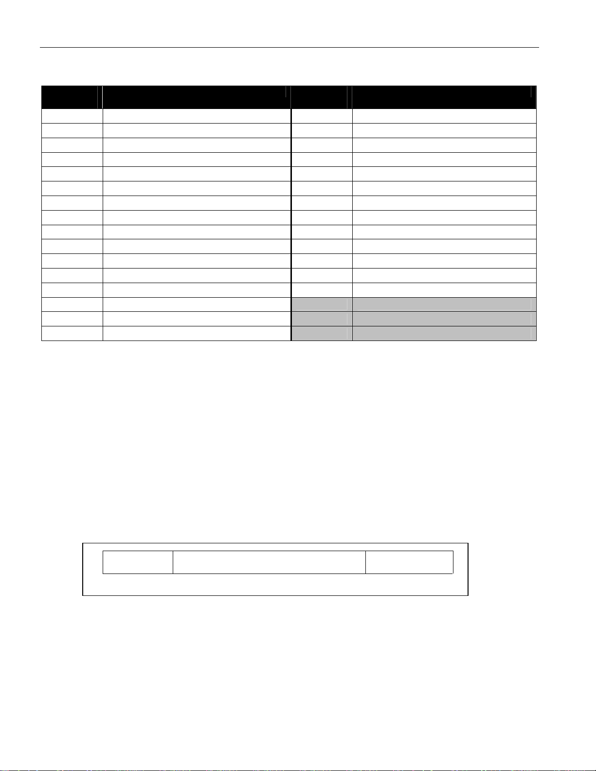
Table 3. PARAMETER EEPROM MEMORY BLOCK 1
ADDRESS
(HEX)
60 CONTROL - Control Register 70 AE 3040 Slope
61 AB - Accumulation Bias 71 AE 2030 Slope
62 AC - Aging Capacity MSB 72 AE 1020 Slope
63 AC - Aging Capacity LSB 73 AE 0010 Slope
64 VCHG - Charge Voltage 74 SE 3040 Slope
65 IMIN - Minimum Charge Current 75 SE 2030 Slope
66 VAE - Active Empty Voltage 76 SE 1020 Slope
67 IAE - Active Empty Current 77 SE 0010 Slope
68 Active Empty 40 78 RSGAIN - Sense Resistor Gain MSB
69 RSNSP - Sense Resistor Prime 79 RSGAIN - Sense Resistor Gain LSB
6A Full 40 MSB 7A RSTC - Sense Resistor Temp. Coeff.
6B Full 40 LSB 7B FRSGAIN - Factory Gain MSB
6C Full 3040 Slope 7C FRSGAIN - Factory Gain LSB
6D Full 2030 Slope 7D Reserved
6E Full 1020 Slope 7E Reserved
6F Full 0010 Slope 7F Reserved
DESCRIPTION ADDRESS
(HEX)
DESCRIPTION
1-WIRE BUS SYSTEM
The 1-Wire bus is a system that has a single bus master and one or more slaves. A multidrop bus is a 1-Wire bus
with multiple slaves. A single-drop bus has only one slave device. In all instances, the DS2780 is a slave device.
The bus master is typically a microprocessor in the host system. The discussion of this bus system consists of four
topics: 64-bit net address, hardware configuration, transaction sequence, and 1-Wire signaling.
64-BIT NET ADDRESS
Each DS2780 has a unique, factory-programmed 1-Wire net address that is 64 bits in length. The first eight bits are
the 1-Wire family code (32h for DS2780). The next 48 bits are a unique serial number. The last eight bits are a
cyclic redundancy check (CRC) of the first 56 bits (see Figure 18). The 64-bit net address and the 1-Wire I/O
circuitry built into the device enable the DS2780 to communicate through the 1-Wire protocol detailed in the 1-Wire
Bus System section of this data sheet.
Figure 18. 1-Wire Net Address Format
8-BIT CRC 48-BIT SERIAL NUMBER
MSb LSb
8-BIT FAMILY
CODE (32h)
CRC GENERATION
The DS2780 has an 8-bit CRC stored in the most significant byte of its 1-Wire net address. To ensure error-free
transmission of the address, the host system can compute a CRC value from the first 56 bits of the address and
compare it to the CRC from the DS2780. The host system is responsible for verifying the CRC value and taking
action as a result. The DS2780 does not compare CRC values and does not prevent a command sequence from
proceeding as a result of a CRC mismatch. Proper use of the CRC can result in a communication channel with a
very high level of integrity.
The CRC can be generated by the host using a circuit consisting of a shift register and XOR gates as shown in
Figure 19, or it can be generated in software. Additional information about the Dallas 1-Wire CRC is available in
22 of 29
Page 23

DS2780 Standalone Fuel Gauge IC
Ω
Application Note 27, Understanding and Using Cyclic Redundancy Checks with Dallas Semiconductor Touch
Memory Products. (This application note can be found on the Maxim/Dallas Semiconductor website at
www.maxim-ic.com.)
In the circuit in Figure 19, the shift register bits are initialized to 0. Then, starting with the least significant bit of the
family code, one bit at a time is shifted in. After the 8th bit of the family code has been entered, then the serial
number is entered. After the 48th bit of the serial number has been entered, the shift register contains the CRC
value.
Figure 19. 1-Wire CRC Generation Block Diagram
MSb
XOR
XOR
LSb
INPUT
XOR
HARDWARE CONFIGURATION
Because the 1-Wire bus has only a single line, it is important that each device on the bus be able to drive it at the
appropriate time. To facilitate this, each device attached to the 1-Wire bus must connect to the bus with open-drain
or tri-state output drivers. The DS2780 uses an open-drain output driver as part of the bidirectional interface
circuitry shown in Figure 20. If a bidirectional pin is not available on the bus master, separate output and input pins
can be connected together.
The 1-Wire bus must have a pullup resistor at the bus-master end of the bus. For short line lengths, the value of
this resistor should be approximately 5kΩ. The idle state for the 1-Wire bus is high. If, for any reason, a bus
transaction must be suspended, the bus must be left in the idle state to properly resume the transaction later. If the
bus is left low for more than 120μs (16μs for overdrive speed), slave devices on the bus begin to interpret the low
period as a reset pulse, effectively terminating the transaction.
The DS2780 can operate in two communication speed modes, standard and overdrive. The speed mode is
determined by the input logic level of the OVD pin; a logic 0 selects standard speed and a logic 1 selects overdrive
speed. The OVD pin must be at a stable logic level of 0 or 1 before initializing a transaction with a reset pulse. All
1-Wire devices on a multinode bus must operate at the same communication speed for proper operation. 1-Wire
timing for both standard and overdrive speeds are listed in the Electrical Characteristics: 1-Wire Interface tables.
Figure 20. 1-Wire Bus Interface Circuitry
BUS MASTER DS2780 1-WIRE PORT
Vpullup
(2.0V to 5.5V)
4.7k
Rx
RX
Tx
RX = RECEIVE
TX = TRANSMIT
0.2μA
(typ)
TX
100Ω
MOSFET
23 of 29
Page 24

DS2780 Standalone Fuel Gauge IC
TRANSACTION SEQUENCE
The protocol for accessing the DS2780 through the 1-Wire port is as follows:
Initialization
Net Address Command
Function Command
Transaction/Data
The sections that follow describe each of these steps in detail.
All transactions of the 1-Wire bus begin with an initialization sequence consisting of a reset pulse transmitted by the
bus master followed by a presence pulse simultaneously transmitted by the DS2780 and any other slaves on the
bus. The presence pulse tells the bus master that one or more devices are on the bus and ready to operate. For
more details, see the 1-Wire Signaling section.
NET ADDRESS COMMANDS
Once the bus master has detected the presence of one or more slaves, it can issue one of the net address
commands described in the following paragraphs. The name of each ROM command is followed by the 8-bit
opcode for that command in square brackets. Figure 21 presents a transaction flowchart of the net address
commands.
Read Net Address [33h or 39h]. This command allows the bus master to read the DS2780’s 1-Wire net address.
This command can only be used if there is a single slave on the bus. If more than one slave is present, a data
collision occurs when all slaves try to transmit at the same time (open drain produces a wired-AND result). The
RNAOP bit in the status register selects the opcode for this command, with RNAOP = 0 indicating 33h, and
RNAOP = 1 indicating 39h.
Match Net Address [55h]. This command allows the bus master to specifically address one DS2780 on the 1-Wire
bus. Only the addressed DS2780 responds to any subsequent function command. All other slave devices ignore
the function command and wait for a reset pulse. This command can be used with one or more slave devices on
the bus.
Skip Net Address [CCh]. This command saves time when there is only one DS2780 on the bus by allowing the
bus master to issue a function command without specifying the address of the slave. If more than one slave device
is present on the bus, a subsequent function command can cause a data collision when all slaves transmit data at
the same time.
Search Net Address [F0h]. This command allows the bus master to use a process of elimination to identify the 1-
Wire net addresses of all slave devices on the bus. The search process involves the repetition of a simple threestep routine: read a bit, read the complement of the bit, then write the desired value of that bit. The bus master
performs this simple three-step routine on each bit location of the net address. After one complete pass through all
64 bits, the bus master knows the address of one device. The remaining devices can then be identified on
additional iterations of the process. See Chapter 5 of the Book of DS19xx i
discussion of a net address search, including an actual example. (This publication can be found on the
Maxim/Dallas Semiconductor website at www.maxim-ic.com.)
Resume [A5h]. This command increases data throughput in multidrop environments where the DS2780 needs to
be accessed several times. Resume is similar to the Skip Net Address command in that the 64-bit net address
does not have to be transmitted each time the DS2780 is accessed. After successfully executing a Match Net
Address command or Search Net Address command, an internal flag is set in the DS2780. When the flag is set,
the DS2780 can be repeatedly accessed through the Resume command function. Accessing another device on the
bus clears the flag, thus preventing two or more devices from simultaneously responding to the Resume command
function.
iButton is a registered trademark of Dallas Semiconductor.
Button® Standards for a comprehensive
24 of 29
Page 25

DS2780 Standalone Fuel Gauge IC
FUNCTION COMMANDS
After successfully completing one of the net address commands, the bus master can access the features of the
DS2780 with any of the function commands described in the following paragraphs. The name of each function is
followed by the 8-bit opcode for that command in square brackets. The function commands are summarized in
Table 4.
Read Data [69h, XX]. This command reads data from the DS2780 starting at memory address XX. The LSb of the
data in address XX is available to be read immediately after the MSb of the address has been entered. Because
the address is automatically incremented after the MSb of each byte is received, the LSb of the data at address XX
+ 1 is available to be read immediately after the MSb of the data at address XX. If the bus master continues to read
beyond address FFh, data is read starting at memory address 00 and the address is automatically incremented
until a reset pulse occurs. Addresses labeled “Reserved” in the memory map contain undefined data values. The
read data command can be terminated by the bus master with a reset pulse at any bit boundary. Reads from
EEPROM block addresses return the data in the shadow RAM. A Recall Data command is required to transfer data
from the EEPROM to the shadow. See the Memory section for more details.
Write Data [6Ch, XX]. This command writes data to the DS2780 starting at memory address XX. The LSb of the
data to be stored at address XX can be written immediately after the MSb of address has been entered. Because
the address is automatically incremented after the MSb of each byte is written, the LSb to be stored at address XX
+ 1 can be written immediately after the MSb to be stored at address XX. If the bus master continues to write
beyond address FFh, the data starting at address 00 is overwritten. Writes to read-only addresses, reserved
addresses and locked EEPROM blocks are ignored. Incomplete bytes are not written. Writes to unlocked EEPROM
block addresses modify the shadow RAM. A Copy Data command is required to transfer data from the shadow to
the EEPROM. See the Memory section for more details.
Copy Data [48h, XX]. This command copies the contents of the EEPROM shadow RAM to EEPROM cells for the
EEPROM block containing address XX. Copy data commands that address locked blocks are ignored. While the
copy data command is executing, the EEC bit in the EEPROM register is set to 1 and writes to EEPROM
addresses are ignored. Reads and writes to non-EEPROM addresses can still occur while the copy is in progress.
The copy data command takes t
transmitted.
Recall Data [B8h, XX]. This command recalls the contents of the EEPROM cells to the EEPROM shadow memory
for the EEPROM block containing address XX.
Lock [6Ah, XX]. This command locks (write-protects) the block of EEPROM containing memory address XX. The
LOCK bit in the EEPROM register must be set to 1 before the lock command is executed. To help prevent
unintentional locks, one must issue the lock command immediately after setting the LOCK bit (EEPROM register,
address 1Fh, bit 06) to a 1. If the LOCK bit is 0 or if setting the lock bit to 1 does not immediately precede the lock
command, the lock command has no effect. The lock command is permanent; a locked block can never be written
again.
time to execute, starting on the next falling edge after the address is
EEC
25 of 29
Page 26

Table 4. Function Commands
COMMAND
Read Data
Write Data
Copy Data
Recall Data
Lock
DESCRIPTION
Reads data from
memory starting at
address XX
Writes data to
memory starting at
address XX
Copies shadow RAM
data to EEPROM
block containing
address XX
Recalls EEPROM
block containing
address XX to RAM
Permanently locks
the block of EEPROM
containing address
XX
DS2780 Standalone Fuel Gauge IC
BUS STATE
COMMAND
PROTOCOL
69h, XX Master Rx
6Ch, XX Master Tx
48h, XX Master Reset None
B8h, XX Master Reset None
6Ah, XX
AFTER
COMMAND
PROTOCOL
Master Reset
BUS DATA
Up to 256 bytes of
Up to 256 bytes of
data
data
None
26 of 29
Page 27

Figure 21. Net Address Command Flow Chart
MASTER TX
RESET PULSE
DS2780 Tx
PRESENCE PULSE
MASTER Tx NET
ADDRESS
COMMAND
33h / 39h
READ
NO NO NO
55h
MATCH
F0h
SEARCH
DS2780 Tx
FAMILY CODE
1 BYTE
DS2780 Tx
SERIAL NUMBER
6 BYTES
DS2780 Tx
CRC
1 BYTE
CLEAR RESUME
MASTER TX
BIT 0
BIT 0
MATCH ?
MASTER TX
BIT 1
DS2780 Tx BIT 0
DS2780 Tx BIT 0
MASTER Tx BIT 0
NO NO
DS2780 Tx BIT 1
DS2780 Tx BIT 1
MASTER Tx BIT 1
YESYES YES
BIT 0
MATCH ?
YESYES
BIT 1
MATCH ?
NO NO
BIT 1
MATCH ?
MASTER TX
FUNCTION
COMMAND
MASTER TX
BIT 63
DS2780 Tx BIT 63
DS2780 Tx BIT 63
MASTER Tx BIT 63
SET
RESUME
FLAG
YES
BIT 63
MATCH ?
NO
CLEAR RESUME
DS2780 Standalone Fuel Gauge IC
CCh
SKIP
CLEAR RESUME
MASTER TX
FUNCTION
COMMAND
YESYES
YES
NO
A5h
RESUME
YES
RESUME
FLAG SET ?
YES
MASTER TX
FUNCTION
COMMAND
NO
NO
27 of 29
Page 28

DS2780 Standalone Fuel Gauge IC
1-WIRE SIGNALING
The 1-Wire bus requires strict signaling protocols to ensure data integrity. The four protocols used by the DS2780
are as follows: the initialization sequence (reset pulse followed by presence pulse), write 0, write 1, and read data.
All of these types of signaling except the presence pulse are initiated by the bus master.
The initialization sequence required to begin any communication with the DS2780 is shown in Figure 22. A
presence pulse following a reset pulse indicates that the DS2780 is ready to accept a net address command. The
bus master transmits (Tx) a reset pulse for t
. The bus master then releases the line and goes into receive mode
RSTL
(Rx). The 1-Wire bus line is then pulled high by the pullup resistor. After detecting the rising edge on the DQ pin,
the DS2780 waits for t
and then transmits the presence pulse for t
PDH
PDL
.
Figure 22. 1-Wire Initialization Sequence
t
RSTL
t
RSTH
t
PDH
DQ
t
PDL
PACK
PACK-
LINE TYPE LEGEND:
BUS MASTER ACTIVE LOW
BOTH BUS MASTER AND
DS2780 ACTIVE LOW
DS2780 ACTIVE LOW
RESISTOR PULLUP
WRITE-TIME SLOTS
A write-time slot is initiated when the bus master pulls the 1-Wire bus from a logic-high (inactive) level to a logic-low
level. There are two types of write-time slots: write 1 and write 0. All write-time slots must be t
1μs minimum recovery time, t
, between cycles. The DS2780 samples the 1-Wire bus line between 15μs and
REC
in duration with a
SLOT
60μs (between 2μs and 6μs for overdrive speed) after the line falls. If the line is high when sampled, a write 1
occurs. If the line is low when sampled, a write 0 occurs (see Figure 23). For the bus master to generate a write 1
time slot, the bus line must be pulled low and then released, allowing the line to be pulled high within 15μs (2μs for
overdrive speed) after the start of the write-time slot. For the host to generate a write 0 time slot, the bus line must
be pulled low and held low for the duration of the write-time slot.
READ-TIME SLOTS
A read-time slot is initiated when the bus master pulls the 1-Wire bus line from a logic-high level to a logic-low level.
The bus master must keep the bus line low for at least 1μs and then release it to allow the DS2780 to present valid
data. The bus master can then sample the data t
slot, the DS2780 releases the bus line and allows it to be pulled high by the external pullup resistor. All read-time
slots must be t
in duration with a 1μs minimum recovery time, t
SLOT
information.
from the start of the read-time slot. By the end of the read-time
RDV
, between cycles. See Figure 23 for more
REC
28 of 29
Page 29

Figure 23. 1-Wire Write- And Read-Time Slots
WRITE 0 SLOT WRITE 1 SLOT
t
SLOT
t
LOW0
t
V
PULLUP
REC
GND
Mode
DS2780 Sample Window
MIN TYP MAX
Standard
15μs
15μs
30μs
Overdrive
2μs
1μs
3μs
READ 0 SLOT READ 1 SLOT
t
SLOT
V
PULLUP
GND
Master Sample Window Master Sample Window
t
RDV
LINE TYPE LEGEND:
Bus master active low
Both bus master and
DS2780 active low
>1μs
>1μs
t
15μs
2μs
t
REC
t
RDV
DS2780 active low
Resistor pullup
DS2780 Standalone Fuel Gauge IC
t
SLOT
LOW1
DS2780 Sample Window
MIN TYP MAX
15μs
1μs
t
SLOT
30μs
3μs
Maxim/Dallas Semiconductor cannot assume responsibility for use of any circuitry other than circuitry entirely embodied in a Maxim/Dallas Semiconductor product.
29 of 29
No circuit patent licenses are implied. Maxim/Dallas Semiconductor reserves the right to change the circuitry and specifications without notice at any time.
Maxim Integrated Products, 120 San Gabriel D rive, Sunnyvale, CA 94086 408-737-7600
The Maxim logo is a registered trademark of Maxim Integrated Products, Inc. The Dallas logo is a registered trademark of Dallas Semiconductor Corporation.
© 2007 Maxim Integrated Products • Printed USA
 Loading...