

Page 1
General Description
The DS2775–DS2778 report available capacity for
rechargeable lithium-ion (Li+) and Li+ polymer (Li-Poly)
batteries in mAh and as a percentage of full. Safe operation is ensured by the integrated Li+ protector. The
DS2776/DS2778 support SHA-1-based challengeresponse authentication in addition to all other DS2775/
DS2777 features.
Precision measurements of voltage, temperature, and
current, along with a cell characteristics table and
application parameters, are used for capacity estimation calculations. The capacity registers report a conservative estimate of the amount of charge that can be
removed given the current temperature, discharge rate,
stored charge, and application parameters.
The DS2775–DS2778 operate from +4.0V to +9.2V for
direct integration into battery packs with two Li+ or LiPoly cells.
In addition to nonvolatile storage for cell compensation
and application parameters, the DS2775–DS2778 offer
16 bytes of EEPROM for use by the host system and/or
pack manufacturer to store battery lot and date tracking
information. The EEPROM can also be used for nonvolatile storage of system and/or battery usage statistics. A Maxim 1-Wire
®
(DS2775/DS2776) or 2-wire
(DS2777/DS2778) interface provides serial communication to access measurement and capacity data registers, control registers, and user memory. The
DS2776/DS2778 use the SHA-1 hash algorithm in a
challenge-response pack authentication protocol for
battery-pack verification.
Applications
Low-Cost Notebooks
UMPCs
DSLR Cameras
Video Cameras
Commercial and Military Radios
Portable Medical Equipment
Features
♦ High-Side nFET Drivers and Protection Circuitry
♦ Precision Voltage, Temperature, and Current
Measurement System
♦ Cell-Capacity Estimation from Coulomb Count,
Discharge Rate, Temperature, and Cell
Characteristics
♦ Estimates Cell Aging Between Learn Cycles
♦ Uses Low-Cost Sense Resistor
♦ Allows Calibration of Gain and Temperature
Coefficient
♦ Programmable Thresholds for Overvoltage and
Overcurrent
♦ Pack Authentication Using SHA-1 Algorithm
(DS2776/DS2778)
♦ 32-Byte Parameter EEPROM
♦ 16-Byte User EEPROM
♦ Maxim 1-Wire Interface with 64-Bit Unique ID
(DS2775/DS2776)
♦ 2-Wire Interface with 64-Bit Unique ID
(DS2777/DS2778)
♦ 3mm x 5mm, 14-Pin TDFN Lead-Free Package
DS2775/DS2776/DS2777/DS2778
2-Cell, Stand-Alone, Li+ Fuel-Gauge IC with
Protector and Optional SHA-1 Authentication
________________________________________________________________
Maxim Integrated Products
1
Ordering Information
19-4688; Rev 4; 6/11
For pricing, delivery, and ordering information, please contact Maxim Direct at 1-888-629-4642,
or visit Maxim’s website at www.maxim-ic.com.
PART PIN-PACKAGE TOP MARK
DS2775G+ 14 TDFN-EP* D2775
DS2775G+T& R 14 TDFN-EP* D2775
DS2776G+ 14 TDFN-EP* D2776
DS776G+T&R 14 TDFN-EP* D2776
DS2777G+ 14 TDFN-EP* D2777
DS2777G+T& R 14 TDFN-EP* D2777
DS2778G+ 14 TDFN-EP* D2778
DS2778G+T& R 14 TDFN-EP* D2778
Note: All devices are specified over the -20°C to +70°C operating temperature range.
+
Denotes a lead(Pb)-free/RoHS-compliant package.
T&R = Tape and reel.
*
EP = Exposed pad.
Selector Guide appears at end of data sheet.
1-Wire is a registered trademark of Maxim Integrated Products, Inc.
Page 2

DS2775/DS2776/DS2777/DS2778
2-Cell, Stand-Alone, Li+ Fuel-Gauge IC with
Protector and Optional SHA-1 Authentication
2 _______________________________________________________________________________________
ABSOLUTE MAXIMUM RATINGS
ELECTRICAL CHARACTERISTICS
(VDD= +4.0V to +9.2V, TA= -20°C to +70°C, unless otherwise noted. Typical values are at TA= +25°C.)
Stresses beyond those listed under “Absolute Maximum Ratings” may cause permanent damage to the device. These are stress ratings only, and functional
operation of the device at these or any other conditions beyond those indicated in the operational sections of the specifications is not implied. Exposure to
absolute maximum rating conditions for extended periods may affect device reliability.
Voltage Range on PLS, CP, CC, DC Pins
Relative to V
SS
.....................................................-0.3V to +18V
Voltage Range on V
DD
, V
IN1
, V
IN2
, SRC Pins
Relative to VSS....................................................-0.3V to +9.2V
Voltage Range on All Other Pins Relative to V
SS
..-0.3V to +6.0V
Continuous Sink Current, PIO, DQ......................................20mA
Continuous Sink Current, CC, DC.......................................10mA
Operating Temperature Range ...........................-20°C to +70°C
Storage Temperature Range .............................-55°C to +125°C
Lead Temperature (soldering, 10s) .................................+300°C
Soldering Temperature (reflow) .......................................+260°C
PARAMETER SYMBOL CONDITIONS MIN TYP MAX UNITS
I
DD0
Supply Current
Temperature Accuracy T
I
DD1
I
DD2
ERR
Voltage Accuracy
Input Resistance (V
Current Resolut ion I
Current Ful l Scale I
Current Gain Error I
Current Offset I
Accumulated Current Offset q
Time-Base Error t
CP Output Voltage (VCP - V
CP Startup Time t
Output High: CC, DC V
Output Low: CC V
Output Low: DC V
IN1
, V
) 15 M
IN2
LSB
FS
GERR
OERR
OERR
ERR
) VGS I
SRC
SCP
OHCP IOH
OLCC IOL
OLDC IOL
DQ, PIO Voltage Range -0.3 +5.5 V
DQ, PIO, SDA, SCL Input
Logic-High
DQ, PIO, SDA, SCL Input
Logic-Low
V
V
OVD Input Logic-High V
OVD Input Logic-Low V
Sleep mode, TA +50°C 3 5
Sleep mode, TA> +50°C 10
Active mode 80 135
Active mode during SHA-1 computation 120 300
-3 +3 °C
2.0V V
IN1
4.6V, 0°C T
2.0V V
4.6V, T
2.0V V
IN1
= +25°C
A
IN1
1.56 μV
-51.2 +51.2 mV
-1 +1 % FS
0°C TA +70°C (Note 1) -9.375 9.375 μVh
0°C TA +70°C (Note 1) -255 0 μVh/Day
0°C TA +50°C -2 +2
-3 +3
= 0.9μA 4.4 4.7 5 V
OUT
CE = 0, DE = 0, CCP = 0.1μF, acti ve mode 200 ms
= 100μA (Note 2) VCP - 0.4 V
= 100μA V
= 100μA V
1.5 V
IH
0.6 V
IL
V
IH
V
IL
4.6V, 2.0V (V
+50°C
A
4.6V, 2.0V (V
4.6V, 2.0V (V
IN2
- V
IN2
IN2
)
IN1
– V
)
IN1
- V
) 4.6V -50 +50
IN1
-35 +35
-22 22
- 0.2 V
BAT
SRC
SRC
SS
+ 0.1 V
+ 0.1 V
+ 0.2 V
μA
mV
%
Page 3
DS2775/DS2776/DS2777/DS2778
2-Cell, Stand-Alone, Li+ Fuel-Gauge IC with
Protector and Optional SHA-1 Authentication
_______________________________________________________________________________________ 3
ELECTRICAL CHARACTERISTICS (continued)
(VDD= +4.0V to +9.2V, TA= -20°C to +70°C, unless otherwise noted. Typical values are at TA= +25°C.)
SHA-1 COMPUTATION TIMING (DS2776/DS2778 ONLY)
(VDD= +4.0V to +9.2V, TA= 0°C to +70°C, unless otherwise noted. Typical values are at TA= +25°C.)
ELECTRICAL CHARACTERISTICS: PROTECTION CIRCUIT
(VDD= +4.0V to +9.2V, TA= 0°C to +50°C, unless otherwise noted. Typical values are at TA= +25°C.)
PARAMETER SYMBOL CONDITIONS MIN TYP MAX UNITS
DQ, PIO, SDA Output Logic-Low V
DQ, PIO Pullup Current I
DQ, PIO, SDA, SCL Pulldown
Current
DQ Input Capacitance C
DQ Sleep Timeout t
PIO, DQ Wake Debounce t
OL
PU
I
PD
DQ
SLEEP
WDB
IOL = 4mA 0.4 V
Sleep mode, V
Active mode, V
50 pF
DQ < VIL 2 9 s
Sleep mode 100 ms
= (VDD - 0.4V) 30 100 200 nA
PIN
= 0.4V 30 100 200 nA
PIN
PARAMETER SYMBOL CONDITIONS MIN TYP MAX UNITS
Computation Time t
COMP
30 m s
PARAMETER SYMBOL CONDITIONS MIN TYP MAX UNITS
Overvoltage Detect V
Charge-Enable Voltage V
Undervoltage Detect V
Overcurrent Detect: Charge V
Overcurrent Detect: Discharge V
Short-Circuit Current Detect V
Overvoltage Delay t
Undervoltage Delay t
Overcurrent Delay t
Short-Circuit Delay t
Charger-Detect Hysteresis V
Test Threshold V
Test Current I
PLS Pulldown Current I
Recovery Current I
OV
CE
UV
COC
DOC
SC
OVD
UVD
OCD
SCD
CD
TST
PPD
RC
VOV = 1110111b 4.438 4.473 4.508
VOV = 1100011b 4.242 4.277 4.312
Relative to VOV -100 mV
Programmable in Control register 0x60h,
UV[1:0] = 10
OC = 11b -60 -75 -90
OC = 00b -12.5 -25 -38
OC = 11b 80 100 120
OC = 00b 25 38 50
SC =1b 240 300 360
SC = 0b 120 150 180
(Note 3) 600 1400 ms
(Note 3) 600 1400 ms
8 10 12 ms
80 120 160 μs
VUV condition 50 mV
COC, DOC condition 0.4 1.0 1.2 V
TP
DOC condition 20 40 80
COC condition -45 -60 -95
Sleep mode 200 400 630 μA
VUV condition, max: V
min: V
= 4.2V, VDD = 2V
PLS
= 15V, VDD = 1.4V;
PLS
2.415 2.450 2.485 V
3.3 8 13 mA
V
mV
mV
mV
μA
Page 4

DS2775/DS2776/DS2777/DS2778
2-Cell, Stand-Alone, Li+ Fuel-Gauge IC with
Protector and Optional SHA-1 Authentication
4 _______________________________________________________________________________________
EEPROM RELIABILITY SPECIFICATION
(VDD= +4.0V to +9.2V, TA= -20°C to +70°C, unless otherwise noted.)
ELECTRICAL CHARACTERISTICS: 1-Wire INTERFACE, STANDARD (DS2775/DS2776 ONLY)
(VDD= +4.0V to +9.2V, TA= -20°C to +70°C.)
ELECTRICAL CHARACTERISTICS: 1-Wire INTERFACE, OVERDRIVE (DS2775/DS2776 ONLY)
(VDD= +4.0V to +9.2V, TA= -20°C to +70°C.)
PARAMETER SYMBOL CONDITIONS MIN TYP MAX UNITS
EEPROM Copy Time t
EEPROM Copy Endurance N
EEC
EEC
PARAMETER SYMBOL CONDITIONS MIN TYP MAX UNITS
Time Slot t
Recovery Time t
Write-Zero Low Time t
Write-One Low Time t
Read Data Valid t
Reset Time High t
Reset Time Low t
Presence-Detect High t
Presence-Detect Low t
SLOT
REC
LOW0
LOW1
RDV
RSTH
RSTL
PDH
PDL
10 ms
TA = +50°C 50,000 Cycles
60 120 μs
1 μs
60 120 μs
1 15 μs
15 μs
480 μs
480 960 μs
15 60 μs
60 240 μs
Time Slot t
Recovery Time t
Write-Zero Low Time t
Write-One Low Time t
Read Data Valid t
Reset Time High t
Reset Time Low t
Presence-Detect High t
Presence-Detect Low t
PARAMETER SYMBOL CONDITIONS MIN TYP MAX UNITS
SLOT
REC
LOW0
LOW1
RDV
RSTH
RSTL
PDH
PDL
6 16 μs
1 μs
6 16 μs
1 2 μs
2 μs
48 μs
48 80 μs
2 6 μs
8 24 μs
Page 5

DS2775/DS2776/DS2777/DS2778
2-Cell, Stand-Alone, Li+ Fuel-Gauge IC with
Protector and Optional SHA-1 Authentication
_______________________________________________________________________________________ 5
ELECTRICAL CHARACTERISTICS: 2-WIRE INTERFACE (DS2777/DS2778 ONLY)
(VDD= +4.0V to +9.2V, TA= -20°C to +70°C.)
Note 1: Accumulation bias and offset bias registers set to 00h. NBEN bit set to 0.
Note 2: Measurement made with V
SRC
= +8V, VGSdriven with external +4.5V supply.
Note 3: Overvoltage (OV) and undervoltage (UV) delays (t
OVD
, t
UVD
) are reduced to zero seconds if the OV or UV condition is
detected within 100ms of entering active mode.
Note 4: Timing must be fast enough to prevent the DS2777/DS2778 from entering sleep mode due to bus low for period > t
SLEEP
.
Note 5: f
SCL
must meet the minimum clock low time plus the rise/fall times.
Note 6: The maximum t
HD:DAT
need only be met if the device does not stretch the low period (t
LOW
) of the SCL signal.
Note 7: This device internally provides a hold time of at least 75ns for the SDA signal (referred to the V
IHMIN
of the SCL signal) to
bridge the undefined region of the falling edge of SCL.
Note 8: Filters on SDA and SCL suppress noise spikes at the input buffers and delay the sampling instant.
Note 9: C
B
is total capacitance of one bus line in pF.
PARAMETER SYMBOL CONDITIONS MIN TYP MAX UNITS
SCL Clock Frequency f
Bus-Free Time Between a STOP
and START Condition
Hold Time (Repeated) START
Condition
Low Period of SCL Clock t
High Period of SCL Clock t
Setup Time for a Repeated
START Condition
Data Hold Time t
Data Setup Time t
Rise Time of Both SDA and SCL
Signals
Fal l Time of Both SDA and SCL
Signals
Setup Time for STOP Condition t
Spike Pulse Widths Suppressed
by Input Filter
Capacitive Load for Each Bus
Line
SCL, SDA Input Capacitance C
(Note 4) 0 400 kHz
SCL
t
1.3 μs
BUF
t
(Note 5) 0.6 μs
HD: STA
1.3 μs
LOW
0.6 μs
HIGH
t
0.6 μs
SU:STA
(Notes 6, 7) 0 0.9 μs
HD:DAT
(Note 6) 100 ns
SU:DAT
t
R
t
F
0.6 μs
SU:STO
(Note 8) 0 50 ns
t
SP
C
(Note 9) 400 pF
B
60 pF
BIN
20 +
0.1C
20 +
0.1C
300 ns
B
300 ns
B
Page 6
DS2775/DS2776/DS2777/DS2778
2-Cell, Stand-Alone, Li+ Fuel-Gauge IC with
Protector and Optional SHA-1 Authentication
6 _______________________________________________________________________________________
Typical Operating Characteristics
(TA = +25°C, unless otherwise noted.)
DISCHARGE-OVERCURRENT
PROTECTION DELAY
DS2775/6/7/8 toc01
DC FET
GATE
2V/div
2V/div
0V
0V
0V
0V
1V/div
20mV/div
DC FET
SOURCE
V
GS
V
SNS
25mΩ
SENSE RESISTOR
WITH DISCHARGEOVERCURRENT
THRESHOLD = 38mV
TIME (ms)
18
161412108642020
CC FET GATE TURN-OFF DURING
CHARGE-OVERCURRENT EVENT
DS2775/6/7/8 toc02
CC FET
GATE
2V/div
2V/div
0V
0V
0V
0V
1V/div
20mV/div
CC FET
SOURCE
V
GS
CC FET
V
SNS
25mΩ
SENSE RESISTOR
WITH CHARGEOVERCURRENT
THRESHOLD = 25mV
TIME (μs)
45
403530252015105050
DC FET GATE TURN-OFF DURING
SHORT-CIRCUIT EVENT
DS2775/6/7/8 toc03
DC FET
GATE
2V/div
0V
0V
0V
0V
2V/div
1V/div
50mV/div
DC FET
SOURCE
V
GS
DC FET
V
SNS
25mΩ
SENSE RESISTOR
WITH SHORT-CIRCUIT
THRESHOLD = 150mV
TIME (μs)
18
161412108642020
SHORT-CIRCUIT PROTECTION
DELAY
DS2775/6/7/8 toc04
DC FET
GATE
2V/div
0V
0V
0V
0V
2V/div
1V/div
100mV/div
DC FET
SOURCE
V
GS
DC FET
V
SNS
25mΩ
SENSE RESISTOR
WITH SHORT-CIRCUIT
THRESHOLD = 150mV
TIME (μs)
180
160140120100806040200 200
VOLTAGE MEASUREMENT
ACCURACY
DS2775/6/7/8 toc05
V
INX
(V)
ACCURACY (mV)
4321
2
4
6
8
10
12
14
16
18
20
0
0
+70°C
-20°C
+25°C
CHARGE-PUMP STARTUP EXITING SLEEP
MODE (V
DD
= 8V NO LOAD ON PK+)
DS2775/6/7/8 toc06
TIME (ms)
VOLTAGE (V)
908010 20 30 50 6040 70
0
2
3
4
5
6
7
8
-2
0 100
2.75V
12.6V
Page 7
DS2775/DS2776/DS2777/DS2778
2-Cell, Stand-Alone, Li+ Fuel-Gauge IC with
Protector and Optional SHA-1 Authentication
_______________________________________________________________________________________
7
Typical Operating Characteristics (continued)
(TA = +25°C, unless otherwise noted.)
CURRENT MEASUREMENT
ACCURACY
125
75
25
-25
ACCURACY (μV)
-75
-125
-0.052
-20°C
+25°C
+70°C
V
(mV)
SNS
0.0480.0280.008-0.012-0.032
CURRENT MEASUREMENT OFFSET
vs. TEMPERATURE
2
1
0
-1
-2
LSB (1.5625μV)
-3
-4
-5
-20
TEMPERATURE (°C)
DS2775/6/7/8 toc07
(mA)
RC
I
IRC vs. V
7
1kΩ RESISTOR FROM PLS TO PK+
6
5
4
3
2
1
0
06
DD
DS2775/6/7/8 toc08
54321
VDD (V)
DS2775/6/7/8 toc09
6040200
Page 8
DS2775/DS2776/DS2777/DS2778
2-Cell, Stand-Alone, Li+ Fuel-Gauge IC with
Protector and Optional SHA-1 Authentication
8 _______________________________________________________________________________________
Pin Description
×
Pin Configuration
TOP VIEW
1CC
+
2V
DD
3DC
4V
IN2
5V
IN1
6VB
7V
SS
PIN NAME FUNCTION
1 CC Charge Control. Charge FET control output.
2 VDD Chip-Supply Input. Bypa ss with 0.1μF to VSS.
3 DC Discharge Control. Discharge FET control output.
4 V
5 V
6 VB Regulated Operating Voltage. B ypas s with 0.1μF to VSS.
Battery Voltage Sense Input 2. Connect to highest voltage potential positive cell terminal through
IN2
decoupl ing network.
Battery Voltage Sense Input 1. Connect to lowe st voltage potential po sit ive cel l terminal through
IN1
decoupl ing network.
DS2775
DS2776
DS2777
DS2778
TDFN
(3mm
5mm)
EP
14 CP
13 SRC
12 SCL/OVD
11 SDA/DQ
10 PLS
9 PIO
8 SNS
7 VSS Device Ground. Chip ground and battery-side sense resistor input.
8 SNS Sense Resistor Connection. Pack-side sense resistor sense input.
9 PIO Programmable I/O. Can be configured as wake input.
10 PLS
11 SDA/DQ
12 SCL/OVD
13 SRC Protection MOSFET Source Connection. U sed a s a reference for the charge pump.
14 CP Charge Pump Output. Generates gate drive voltage for protection FETs. Bypass with 0.47μF to SRC.
— EP Exposed Pad. Connect to ground or leave unconnected.
Pack Plus Terminal Sense Input. Used to detect the removal of short-circuit, discharge overcurrent, and
charge overcurrent condition s.
Data Input/Output. Serial data I/O, includes weak pulldown to detect system disconnect and can be
configured as wa ke input for 1-Wire devices.
Serial Clock Input/Overdrive Select. Communication clock for 2-wire devices/overdrive select pin for
1-Wire devices.
Page 9
DS2775/DS2776/DS2777/DS2778
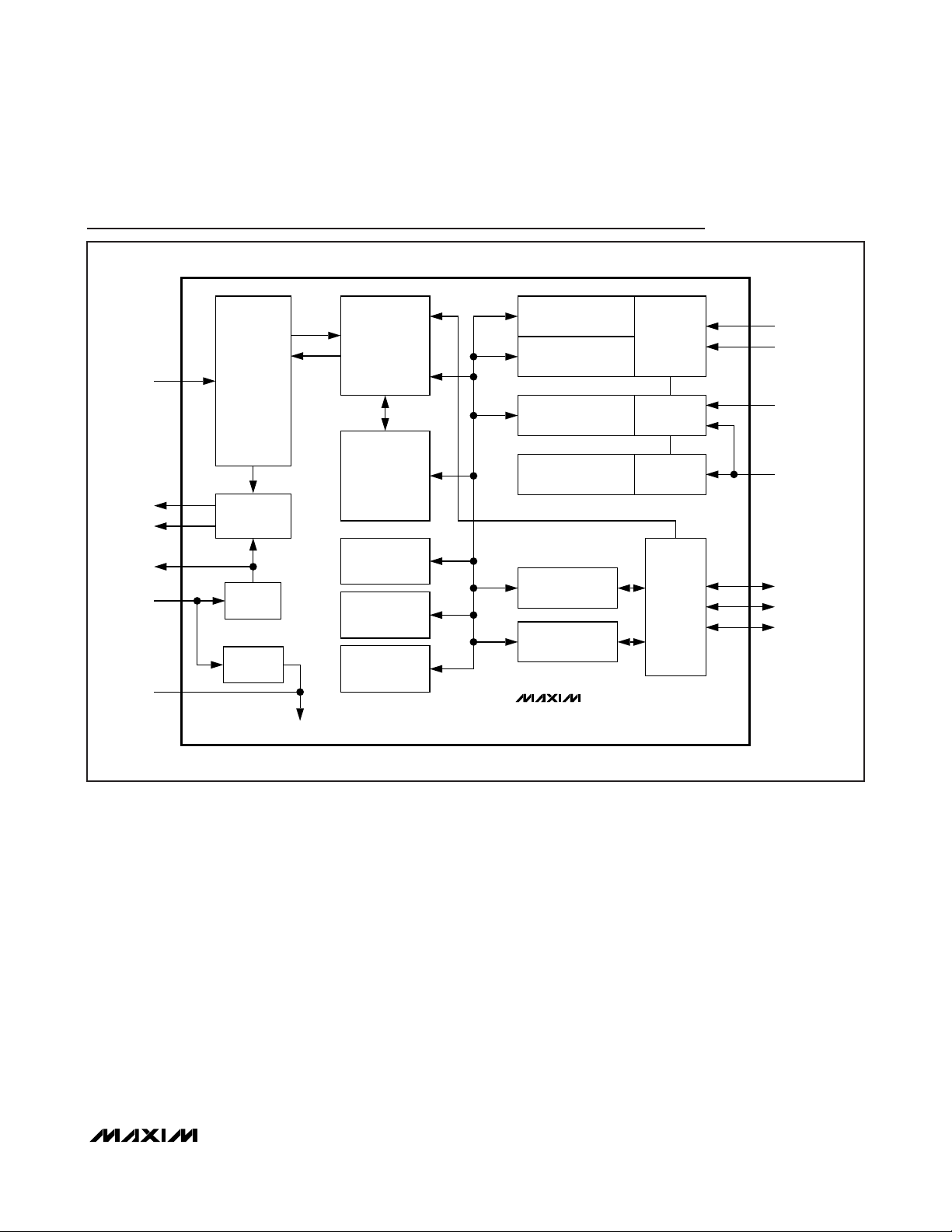
Block Diagram
FuelPack is a trademark of Maxim Integrated Products, Inc.
2-Cell, Stand-Alone, Li+ Fuel-Gauge IC with
Protector and Optional SHA-1 Authentication
_______________________________________________________________________________________ 9
PLS
CC
DC
CP
V
VOLTAGE
POWER-MODE
CONTROL
Li+
PROTECTOR
FuelPack™
ALGORITHM
FET DRIVERS
CONTROL AND
STATUS REGISTERS
DD
VB
CHARGE
PUMP
VOLTAGE
REGULATOR
VB INTERNAL
32-BYTE
PARAMETER
EEPROM
16-BYTE USER
EEPROM
TEMPERATURE
CURRENT
PRECISION ANALOG
OSCILLATOR
PIO LOGIC
COMMUNICATION
INTERFACE
DS2775–DS2778
10-BIT + SIGN
ADC/MUX
15-BIT + SIGN
ADC
VREF
PIN
DRIVERS
AND
POWER
SWITCH
CONTROL
V
IN2
V
IN1
SNS
V
SS
SDA/DQ
SCL/OVD
PIO
Page 10
DS2775/DS2776/DS2777/DS2778
2-Cell, Stand-Alone, Li+ Fuel-Gauge IC with
Protector and Optional SHA-1 Authentication
10 ______________________________________________________________________________________
DS2775/DS2776 Typical Application Circuit
DS2777/DS2778 Typical Application Circuit
PK+
1kΩ 150Ω
150Ω
DATA
5.1V
0.1μF
PK-
1kΩ
CC SRC DC
PLS
DQ
DS2775
PIO
VB
DS2776
R
SNS
1kΩ470Ω
V
DD
V
IN2
V
IN1
CP
V
OVDSNS
SS
SRC
PK+
1kΩ 150Ω
1kΩ
1kΩ470Ω
0.47μF
1kΩ
1kΩ
0.1μF
1kΩ
CC SRC DC
SDA
SCL
PK-
150Ω
150Ω
PLS
SDA
SCL
PIO
5.1V5.1V
0.1μF
VB
SNS
DS2777
DS2778
R
SNS
V
DD
V
IN2
V
IN1
CP
SRC
0.47μF
0.1μF
V
SS
1kΩ
Page 11

DS2775/DS2776/DS2777/DS2778
2-Cell, Stand-Alone, Li+ Fuel-Gauge IC with
Protector and Optional SHA-1 Authentication
______________________________________________________________________________________ 11
Detailed Description
The DS2775–DS2778 function as an accurate fuel
gauge, Li+ protector, and SHA-1-based authentication
token (SHA-1-based authentication available only on
the DS2776/DS2778). The fuel gauge provides accurate estimates of remaining capacity and reports timely
voltage, temperature, and current measurement data.
Capacity estimates are calculated from a piecewise linear model of the battery performance over load and
temperature along with system parameters for charge
and end-of-discharge conditions. The algorithm parameters are user programmable and can be modified
within the pack. Critical capacity and aging data are
periodically saved to EEPROM in case of short-circuit
or deep-depletion events.
The Li+ protection function ensures safe, high-performance operation. nFET protection switches are driven
with a charge pump that maintains gate drive as the
cell voltage decreases. The high-side topology preserves the ground path for serial communication while
eliminating the parasitic charge path formed when the
fuel-gauge IC is located inside the protection FETs in a
low-side configuration. The thresholds for overvoltage,
undervoltage, overcurrent, and short-circuit current are
user programmable for customization to each cell and
application.
The 32-bit-wide SHA-1 engine with 64-bit secret and
64-bit challenge words resists brute force and other
attacks with financial-level HMAC security. The challenge of managing secrets in the supply chain is
addressed with the compute next secret feature. The
unique serial number or ROM ID can be used to assign
a unique secret to each battery.
Power Modes
The DS2775–DS2778 have two power modes: active
and sleep. On initial power-up, the DS2775–DS2778
default to active mode. In active mode, the DS2775–
DS2778 are fully functional with measurements and
capacity estimation registers continuously updated.
The protector circuit monitors battery pack, cell voltages, and battery current for safe conditions. The protection FET gate drivers are enabled when conditions
are deemed safe. Also, the SHA-1 authentication function is available in active mode. When an SHA-1 computation is performed, the supply current increases to
I
DD2
for t
SHA
. In sleep mode, the DS2775–DS2778 con-
serve power by disabling measurement and capacity
estimation functions, but preserve register contents.
Gate drive to the protection FETs is disabled in sleep;
the SHA-1 authentication feature is not operational.
The IC enters sleep mode under two different conditions: bus low and undervoltage. An enable bit makes
entry into sleep optional for each condition. Sleep mode
is not entered if a charger is connected (V
PLS
> VDD+
V
CD
) or if a charge current of 1.6mV/R
SNS
measured
from SNS to V
SS
. The DS2775–DS2778 exit sleep mode
upon charger connection or a low-to-high transition on
any communication line. The bus-low condition, where
all communication lines are low for t
SLEEP
, indicates
pack removal or system shutdown in which the bus
pullup voltage, V
PULLUP
, is not present. The power
mode (PMOD) bit must be set to enter sleep when a
bus-low condition occurs. After the DS2775–DS2778
enter sleep due to a bus-low condition, it is assumed
that no charge or discharge current flows and that
coulomb counting is unnecessary.
The second condition to enter sleep is an undervoltage
condition, which reduces battery drain due to the
DS2775–DS2778 supply current and prevents overdischarging the cell. The DS2775–DS2778 transition to
sleep mode if the V
IN1
or V
IN2
voltage is less than V
UV
and the undervoltage enable (UVEN) bit is set. The
communication bus must be in a static state, that is,
with DQ (SDA and SCL for 2-wire) either high or low for
t
SLEEP
. The DS2775–DS2778 transition from sleep
mode to active mode when DQ (SDA and SCL for
2-wire) changes logic state. See Figures 1 and 2 for
more information on sleep-mode state.
The DS2775–DS2778 have a “power switch” capability
for waking the device and enabling the protection FETs
when the host system is powered down. A simple dry
contact switch on the PIO pin or DQ pin can be used to
wake up the battery pack. The power-switch function is
enabled using the PSPIO and PSDQ configuration bits
in the Control register.
When PSPIO or PSDQ are set and sleep mode is
entered through the PMOD condition*, the PIO and DQ
pins pull high, respectively. Sleep mode is exited upon
the detection of a low-going transition on PIO or DQ.
PIO has a 100ms debounce period to filter out glitches
that can be caused when a sleeping battery is inserted
into a system.
*
The “power switch” feature is disabled if sleep mode is
entered because of a UV condition.
Page 12
DS2775/DS2776/DS2777/DS2778
2-Cell, Stand-Alone, Li+ Fuel-Gauge IC with
Protector and Optional SHA-1 Authentication
12 ______________________________________________________________________________________
Li+ Protection Circuitry
During active mode, the DS2775–DS2778 constantly
monitor SNS, V
IN1
, V
IN2
, and PLS to protect the battery
from overvoltage (overcharge), undervoltage (overdischarge), and excessive charge and discharge currents
(overcurrent, short circuit). Table 1 summarizes the
conditions that activate the protection circuit, the
response of the DS2775–DS2778, and the thresholds
that release the DS2775–DS2778 from a protection
state. Figure 3 shows Li+ protection circuitry example
waveforms.
Overvoltage (OV)
If either of the voltages on (V
IN2
- V
IN1
) or (V
IN1
- VSS)
exceeds the overvoltage threshold, VOV, for a period
longer than overvoltage delay, t
OVD
, the CC pin is driven low to shut off the external charge FET. The DC output remains high during overvoltage to allow
discharging. When (V
IN2
- V
IN1
) and (V
IN1
- VSS) falls
below the charge-enable threshold, VCE, the
DS2775–DS2778 turn the charge FET on by driving CC
high. The DS2775–DS2778 drive CC high before
[(V
IN2-VIN1
) and (V
IN1
- VSS)] < VCEif a discharge
condition persists with V
SNS
≥ 1.2mV and [(V
IN2
- V
IN1
)
and (V
IN1
- VSS)] < VOV.
ACTIVE
PMOD = 0
UVEN = 0
SLEEP
PSPIO = 0
PSDQ = 0
RISING EDGE ON DQ
CHARGER DETECT
PULL DQ LOW
CHARGER DETECT
ACTIVE
PMOD = 0
UVEN = 1
SLEEP
PSPIO = 0
PSDQ = 1
V
IN1
OR V
IN2
< V
UV
PULL PIO LOW
RISING EDGE ON DQ
CHARGER DETECT
ACTIVE
PMOD = 1
UVEN = 0
SLEEP
PSPIO = 1
PSDQ = 0
PULL DQ LOW FOR t
SLEEP
PULL DQ LOW FOR t
SLEEP
PULL DQ LOW
PULL PIO LOW
CHARGER DETECT
ACTIVE
PMOD = 1
UVEN = 1
SLEEP
PSPIO = 1
PSDQ = 1
V
IN1
OR V
IN2
< V
UV
Figure 1. Sleep-Mode State Diagram for DS2775/DS2776
ACTIVE
PMOD = 0
UVEN = 0
SLEEP
PSPIO = 0
PSDQ = X
RISING EDGE ON SDA OR SCL
CHARGER DETECT
V
IN1
OR V
IN2
< V
UV
CHARGER DETECT
ACTIVE
PMOD = 0
UVEN = 1
SLEEP
PSPIO = 0
PSDQ = X
RISING EDGE ON SDA OR SCL
PULL PIO LOW
CHARGER DETECT
PULL SDA AND SCL LOW
FOR t
SLEEP
ACTIVE
PMOD = 1
UVEN = 0
SLEEP
PSPIO = 1
PSDQ = X
RISING EDGE ON SDA OR SCL
PULL SDA AND SCL LOW
FOR t
SLEEP
PULL PIO LOW
CHARGER DETECT
V
IN1
OR V
IN2
< V
UV
ACTIVE
PMOD = 1
UVEN = 1
SLEEP
PSPIO = 1
PSDQ = X
RISING EDGE ON SDA OR SCL
Figure 2. Sleep-Mode State Diagram for DS2777/DS2778
Page 13
DS2775/DS2776/DS2777/DS2778
2-Cell, Stand-Alone, Li+ Fuel-Gauge IC with
Protector and Optional SHA-1 Authentication
______________________________________________________________________________________ 13
Table 1. Li+ Protection Conditions and DS2775/DS2776 Responses
Note 1: V
CELL
is defined as (V
IN1
- VSS) or (V
IN2
- V
IN1
).
Note 2: Sleep mode is only entered if UVEN = 1.
Note 3: If V
CELL
< VUVwhen a charger connection is detected, release is delayed until V
CELL
≥
V
UV
. The recovery charge path pro-
vides an internal current limit (I
RC
) to safely charge the battery.
Note 4: With test current I
PPD
flowing from PLS to VSS(pulldown on PLS) enabled.
Note 5: With test current I
TST
flowing from VDDto PLS (pullup on PLS).
V
OV
V
CE
V
UV
V
IN
V
SNS
-V
COC
0
V
DOC
V
SC
t
OVD
t
OVD
t
OCD
t
UVD
t
UVD
t
OCD
t
SCO
DISCHARGE
CHARGE
POWER
MODE
ACTIVE
SLEEP*
*IF UVEN = 1.
CC
DC
V
OHCC
V
CP
V
DD
V
CP
V
PLS
Figure 3. Li+ Protection Circuitry Example Waveforms
ACTIVATION
CC Off
OVD
UVD
CC Off, DC Off
OCD
DC Off
OCD
DC Off V
SCD
CC Off, DC Off,
Sleep Mode (Note 2)
CONDITION
Overvoltage (OV) (Note 1) V
Undervoltage (UV) (Note 1) V
Overcurrent, Charge (COC) V
Overcurrent, Discharge
(DOC)
Short Circuit (SC) V
THRESHOLD DELAY RESPONSE
> VOV t
CELL
< VUV t
CELL
< V
SNS
COC
V
> V
SNS
DOC
> VSC t
SNS
t
t
RELEASE THRESHOLD
< VCE or
CELL
1.2mV and both
< VOV) (Note 1)
(charger connected)
> VUV and
CELL
V
PLS
Both V
(V
SNS
V
CELL
> V
IN2
or (both V
UVEN = 0) (Note 3)
V
< VDD – V
PLS
TP
(charger removed) (Note 4)
> VDD – V
V
PLS
TP
(load removed) (Note 5)
> VDD – VTP (Note 5)
PLS
Page 14
DS2775/DS2776/DS2777/DS2778
2-Cell, Stand-Alone, Li+ Fuel-Gauge IC with
Protector and Optional SHA-1 Authentication
14 ______________________________________________________________________________________
Undervoltage (UV)
If the average of the voltages on (V
IN2
- V
IN1
) or
(V
IN1
- VSS) drops below the undervoltage threshold,
VUV, for a period longer than undervoltage delay, t
UVD
,
the DS2775–DS2778 shut off the charge and discharge
FETs. If UVEN is set, the DS2775–DS2778 also enter
sleep mode. When a charger is detected and V
PLS
>
V
IN2
, the DS2775–DS2778 provide a current-limited
recovery charge path (IRC) from PLS to VDDto gently
charge severely depleted cells. The recovery charge
path is enabled when 0 ≤ [(V
IN2
- V
IN1
) and (V
IN1
-
V
SS
)] < VCE. The FETs remain off until (V
IN2
- V
IN1
) and
(V
IN1
- VSS) exceed VUV.
Overcurrent, Charge Direction (COC)
Charge current develops a negative voltage on V
SNS
with respect to VSS. If V
SNS
is less than the charge
overcurrent threshold, V
COC
, for a period longer than
overcurrent delay, t
OCD
, the DS2775–DS2778 shut off
both external FETs. The charge current path is not reestablished until the voltage on the PLS pin drops
below (VDD- VTP). The DS2775–DS2778 provide a test
current of value I
PPD
from PLS to VSS, pulling PLS
down, in order to detect the removal of the offending
charge current source.
Overcurrent, Discharge Direction (DOC)
Discharge current develops a positive voltage on V
SNS
with respect to VSS. If V
SNS
exceeds the discharge
overcurrent threshold, V
DOC
, for a period longer than
t
OCD
, the DS2775–DS2778 shut off the external discharge FET. The discharge current path is not reestablished until the voltage on PLS rises above (VDD- VTP).
The DS2775–DS2778 provide a test current of value
I
TST
from V
DD
to PLS, pulling PLS up, in order to detect
the removal of the offending low-impedance load.
Short Circuit (SC)
If V
SNS
exceeds short-circuit threshold, VSC, for a
period longer than short-circuit delay, t
SCD
, the
DS2775–DS2778 shut off the external discharge FET.
The discharge current path is not reestablished until
the voltage on PLS rises above (VDD- VTP). The
DS2775–DS2778 provide a test current of value I
TST
from VDDto PLS, pulling PLS up, in order to detect the
removal of the short circuit.
All the protection conditions described are logic
ANDed to affect the CC and DC outputs.
CC = (overvoltage) AND (undervoltage) AND
(overcurrent, charge direction) AND (Protection register
bit CE = 0)
DC = (undervoltage) AND (overcurrent, either direction)
AND (short circuit) AND (Protection register bit
DE = 0)
Voltage Measurements
Cell voltages are measured every 440ms. The lowest
potential cell, V
IN1
, is measured with respect to VSS.
The highest potential cell, V
IN2
, is measured with
respect to V
IN1
. Battery voltages are measured with a
range of -5V to +4.9951V and a resolution of 4.8828mV
and placed in the Result register in two’s complement
form. Voltages above the maximum register value are
reported as 7FE0h.
MSB - ADDRESS 0Ch, V
IN1
- V
SS
LSB - ADDRESS 0Dh, V
IN1
- V
SS
MSB - ADDRESS 1Ch, V
IN2
- V
IN1
LSB - ADDRESS 1Dh, V
IN2
- V
IN1
S 29 28 27 26 25 24 2
3
22 21 20 X X X X X
MSb LSb MSb LSb
“S”: SIGN BIT(S), “X”: RESERVED UNITS: 4.883mV
Figure 4. Voltage Register Format
Page 15

DS2775/DS2776/DS2777/DS2778
2-Cell, Stand-Alone, Li+ Fuel-Gauge IC with
Protector and Optional SHA-1 Authentication
______________________________________________________________________________________ 15
Temperature Measurement
The DS2775–DS2778 use an integrated temperature
sensor to measure battery temperature with a resolution
of 0.125°C. Temperature measurements are updated
every 440ms and placed in the Temperature register in
two’s complement form.
Current Measurement
In active mode, the DS2775–DS2778 continuously measure the current flow into and out of the battery by measuring the voltage drop across a low-value current-sense
resistor, R
SNS
. The voltage-sense range between SNS
and V
SS
is ±51.2mV with a least significant bit (LSb) of
1.5625µV. The input linearly converts peak signal amplitudes up to 102.4mV as long as the continuous signal
level (average over the conversion cycle period) does
not exceed ±51.2mV. The ADC samples the input differentially at 18.6kHz and updates the Current register at
the completion of each conversion cycle (3.52s). Charge
currents above the maximum register value are reported
as 7FFFh. Discharge currents below the minimum register value are reported as 8000h.
The Average Current register reports an average current level over the preceding 28.16s. The register value
is updated every 28.16s in two’s complement form and
represents an average of the eight preceding Current
register values.
MSB—ADDRESS 0Ah LSB—ADDRESS 0Bh
S 2
9
28 27 26 25 24 2
3
22 21 20 X X X X X
MSb LSb MSb LSb
“S”: SIGN BIT(S), “X”: RESERVED UNITS: 0.125°C
Figure 5. Temperature Register Format
MSB—ADDRESS 0Eh LSB—ADDRESS 0Fh
S 2
14
213 212 211 210 29 2
8
27 26 25 24 23 22 21 2
0
MSb LSb MSb LSb
“S”: SIGN BIT(S)
UNITS: 1.5625μV/R
SNS
Figure 6. Current Register Format
MSB—ADDRESS 08h LSB—ADDRESS 09h
S 2
14
213 212 211 210 29 2
8
27 26 25 24 23 22 21 2
0
MSb LSb MSb LSb
“S”: SIGN BIT(S)
UNITS: 1.5625μV/R
SNS
Figure 7. Average Current Register Format
Page 16

DS2775/DS2776/DS2777/DS2778
2-Cell, Stand-Alone, Li+ Fuel-Gauge IC with
Protector and Optional SHA-1 Authentication
16 ______________________________________________________________________________________
Current Offset Correction
Every 1024th conversion, the ADC measures its input
offset to facilitate offset correction. Offset correction
occurs approximately once per hour. The resulting correction factor is applied to the subsequent 1023 measurements. During the offset correction conversion, the
ADC does not measure the sense resistor signal. A
maximum error of 1/1024 in the Accumulated Current
register (ACR) is possible; however, to reduce the error,
the current measurement made just prior to the offset
conversion is retained in the Current register and is
substituted for the dropped current measurement in the
current accumulation process. Therefore the accumulated current error due to offset correction is typically
much less than 1/1024.
Current Offset Bias
The current offset bias value (COB) allows a programmable offset value to be added to raw current measurements. The result of the raw current measurement plus
COB is displayed as the current measurement result in
the Current register and is used for current accumulation. COB can be used to correct for a static offset error
or can be used to intentionally skew the current results
and therefore the current accumulation. Read and write
access is allowed to COB. Whenever the COB is written, the new value is applied to all subsequent current
measurements. COB can be programmed in 1.56µV
steps to any value between -199.7µV and +198.1µV.
The COBR value is stored as a two’s complement value
in volatile memory and must be initialized through the
interface on power-up. The factory default value is 00h.
Current Blanking
The current blanking feature modifies current measurement result prior to being accumulated in the ACR.
Current blanking occurs conditionally when a current
measurement (raw current and COBR) falls in one of
two defined ranges. The first range prevents charge
currents less than 100µV from being accumulated. The
second range prevents discharge currents less than
25µV in magnitude from being accumulated. Charge
current blanking is always performed; however, discharge current blanking must be enabled by setting the
NBEN bit in the Control register. See the
Control
Register Format
description for additional information.
Current Measurement Gain
The DS2775–DS2778’s current measurement gain can
be adjusted through the RSGAIN register, which is factory calibrated to meet the data sheet specified accuracy.
RSGAIN is user accessible and can be reprogrammed
after module or pack manufacture to improve the current
measurement accuracy. Adjusting RSGAIN can correct
for variation in an external sense resistor’s nominal value
and allows the use of low-cost, nonprecision currentsense resistors. RSGAIN is an 11-bit value stored in 2
bytes of the parameter EEPROM memory block. The
RSGAIN value adjusts the gain from 0 to 1.999 in steps
of 0.001 (precisely 2–10). The user must use caution
when programming RSGAIN to ensure accurate current
measurement. When shipped from the factory, the gain
calibration value is stored in two separate locations in the
parameter EEPROM block, RSGAIN, which is reprogrammable and FRSGAIN, which is read-only. RSGAIN determines the gain used in the current measurement. The
ADDRESS 7Bh
S 2
6
25 24 23 22 21 2
0
MSb LSb
“S”: SIGN BIT(S)
UNITS: 1.56μV/R
SNS
Figure 8. Current Offset Bias Register Format
MSB—ADDRESS 78h LSB—ADDRESS 79h
X SC0 OC1 OC0 X 2
0
2-1 2
-2
2-3 2-4 2-5 2-6 2-7 2-8 2-9 2
-10
MSb LSb MSb LSb
“X”: RESERVED UNITS: 2–10
Figure 9. RSGAIN Register
Page 17
DS2775/DS2776/DS2777/DS2778
2-Cell, Stand-Alone, Li+ Fuel-Gauge IC with
Protector and Optional SHA-1 Authentication
______________________________________________________________________________________ 17
FRSGAIN value is provided to preserve the factory calibration value only and is not used to calibrate the current
measurement. The 16-bit FRSGAIN value is readable
from addresses B0h and B1h.
Sense-Resistor Temperature
Compensation
The DS2775–DS2778 can temperature compensate the
current-sense resistor to correct for variation in a sense
resistor’s value over temperature. The DS2775–DS2778
are factory programmed with the sense-resistor temperature coefficient, RSTC, set to zero, which turns off the
temperature compensation function. RSTC is user
accessible and can be reprogrammed after module or
pack manufacture to improve the current accuracy
when using a high-temperature coefficient currentsense resistor. RSTC is an 8-bit value stored in the
parameter EEPROM memory block. The RSTC value
sets the temperature coefficient from 0 to +7782ppm/°C
in steps of 30.5ppm/°C. The user must program RSTC
cautiously to ensure accurate current measurement.
Temperature compensation adjustments are made when
the Temperature register crosses 0.5°C boundaries. The
temperature compensation is most effective with the
resistor placed as close as possible to the VSSterminal
to optimize thermal coupling of the resistor to the on-chip
temperature sensor. If the current shunt is constructed
with a copper PCB trace, run the trace under the
DS2775–DS2778 package whenever possible.
Current Accumulation
Current measurements are internally summed, or accumulated, at the completion of each conversion period
with the results displayed in the Accumulated Current
register (ACR). The accuracy of the ACR is dependent
on both the current measurement and the conversion
time base. The ACR has a range of 0 to +409.6mVh
with an LSb of 6.25µVh. Additional registers hold fractional results of each accumulation to avoid truncation
errors. The fractional result bits are not user accessible.
Accumulation of charge current above the maximum
register value is reported at the maximum value; conversely, accumulation of discharge current below the
minimum register value is reported at the minimum
value.
Charge currents (positive Current register values) less
than 100µV are not accumulated in order to mask the
effect of accumulating small positive offset errors over
long periods. This effect limits the minimum charge current, for coulomb counting purposes, to 5mA for R
SNS
= 0.020Ω and 20mA for R
SNS
= 0.005Ω (see Table 2 for
more details).
Read and write access is allowed to the ACR. The
ACR must be written most significant byte (MSB) first,
then LSB. Whenever the ACR is written, the fractional
accumulation result bits are cleared. The write must
be completed in 3.5s. A write to the ACR forces the
ADC to perform an offset correction conversion and
update the internal offset correction factor. The current measurement and accumulation begin with the
second conversion following a write to the ACR. To
preserve the ACR value in case of power loss, the
ACR value is backed up to EEPROM. The ACR value
is recovered from EEPROM on power-up. See the
Memory Map
for specific address location and back-
up frequency.
Table 2. Resolution and Range vs. Sense Resistor
MSB—ADDRESS 10h LSB—ADDRESS 11h
2
15
214 213 212 211 210 29 2
8
27 26 25 24 23 22 21 2
0
MSb LSb MSb LSb
UNITS: 6.25μV/R
SNS
Figure 10. Accumulated Current Register Format
R
TYPE OF RESOLUTION/RANGE VSS - V
Current Resolution 1.5625μV 78.13μA 104.2μA 156.3μA 312.5μA
Current Range ±51.2mV ±2.56A ±3.41A ±5.12A ±10.2A
ACR Resolution 6.25μVh 312.5μAh 416.7μAh 625μAh 1.250mAh
ACR Range ±409.6mVh ±20.48Ah ±27.30Ah ±40.96Ah ±81.92Ah
SNS
20m 15m 10m 5m
SNS
Page 18

DS2775/DS2776/DS2777/DS2778
2-Cell, Stand-Alone, Li+ Fuel-Gauge IC with
Protector and Optional SHA-1 Authentication
18 ______________________________________________________________________________________
Accumulation Bias
In some designs a systematic error or an application
preference requires the application of an arbitrary bias
to the current accumulation process. The Current
Accumulation Bias register (CAB) allows a user-programmed constant positive or negative polarity bias to
be included in the current accumulation process. The
value in CAB can be used to estimate battery currents
that do not flow through the sense resistor, estimate
battery self-discharge, or estimate current levels below
the current measurement resolution. The user-programmed two’s complement value, with bit weighting
the same as the current register, is added to the ACR
once per current conversion cycle. CAB is loaded on
power-up from EEPROM memory.
Cycle Counter
The cycle counter is an absolute count of the cumulative discharge cycles. This register is intended to act as
a “cell odometer.” The LSb is two cycles, which allows
a maximum count of 510 discharge cycles. The register
does not loop. Once the maximum value is reached,
the register is clamped. This register is read and write
accessible while the parameter EEPROM memory block
(block 1) is unlocked. The Cycle Count register
becomes read-only once the EEPROM block is locked.
Capacity Estimation Algorithm
Remaining capacity estimation uses real-time measured values and stored parameters describing the cell
characteristics and application operating limits. Figure
13 describes the algorithm inputs and outputs.
Modeling Cell Characteristics
To achieve reasonable accuracy in estimating remaining capacity, the cell performance characteristics over
temperature, load current, and charge-termination point
must be considered. Since the behavior of Li+ cells is
nonlinear, these characteristics must be included in the
capacity estimation to achieve an acceptable level of
accuracy in the capacity estimation. The FuelPack
method used in the DS2775–DS2778 is described in
general in Application Note 131:
Lithium-Ion Cell Fuel
Gauging with Maxim Battery Monitor ICs.
To facilitate
efficient implementation in hardware, a modified version
of the method outlined in Application Note 131 is used
to store cell characteristics in the DS2775–DS2778. Full
and empty points are retrieved in a lookup process that
retraces a piecewise linear model consisting of three
model curves named full, active empty, and standby
empty. Each model curve is constructed with five line
segments, numbered 1 through 5. Above +40°C, the
segment 5 model curves extend infinitely with zero
slope, approximating the nearly flat change in capacity
of Li+ cells at temperatures above +40°C. Segment 4 of
each model curves originates at +40°C on its upper end
and extends downward in temperature to the junction
with segment 3. Segment 3 joins with segment 2, which
in turn joins with segment 1. Segment 1 of each model
curve extends from the junction with segment 2 to infinitely colder temperatures. The three junctions or breakpoints that join the segments (labeled TBP12, TBP23,
and TBP34 in Figure 14) are programmable in 1°C
increments from -128°C to +40°C. The slope or derivative for segments 1, 2, 3, and 4 are also programmable
over a range of 0 to 15,555ppm in steps of 61ppm.
ADDRESS 61h
S 2
6
25 24 23 22 21 2
0
MSb LSb
“S”: SIGN BIT(S)
UNITS: 6.25μV/R
SNS
Figure 11. Current Accumulation Bias Register Format
ADDRESS 1Eh
2
7
26 25 24 23 22 21 2
0
MSb LSb
UNITS: 2 cycle s
Figure 12. Cycle Counter Register Format
Page 19

DS2775/DS2776/DS2777/DS2778
2-Cell, Stand-Alone, Li+ Fuel-Gauge IC with
Protector and Optional SHA-1 Authentication
______________________________________________________________________________________ 19
Figure 13. Top-Level Algorithm Diagram
Full
The full curve defines how the full point of a given cell
depends on temperature for a given charge termination. The application’s charge termination method
should be used to determine the table values. The
DS2775–DS2778 reconstruct the full line from cell characteristic table values to determine the full capacity of
the battery at each temperature. Reconstruction occurs
in one-degree temperature increments.
Active Empty
The active-empty curve defines the variation of the
active-empty point over temperature. The active-empty
point is defined as the minimum voltage required for
system operation at a discharge rate based on a highlevel load current (one that is sustained during a highpower operating mode). This load current is
programmed as the active-empty current (IAE), and
should be a 3.5s average value to correspond to values
VOLTAGE (R) FULL FULL(T) (R)
TEMPERATURE (R)
CURRENT (R)
ACCUMULATED
CURRENT (ACR) (RW)
AVERAGE CURRENT (R)
CELL MODEL PARAMETERS
(EEPROM)
AGING CAPACITY (AC)
(2 BYTES EE)
AGE SCALAR (AS)
(1 BYTE EE)
SENSE-RESISTOR PRIME (RSNSP)
(1 BYTE EE)
CHARGE VOLTAGE (VCHG)
(1 BYTE EE)
MINIMUM CHARGE CURRENT (IMIN)
(1 BYTE EE)
CAPACITY LOOKUP
AVAILABLE CAPACITY CALCULATION
ACR HOUSEKEEPING
AGE ESTIMATOR
LEARN FUNCTION
ACTIVE EMPTY AE(T) (R)
STANDBY EMPTY SE(T) (R)
REMAINING ACTIVE-ABSOLUTE
CAPACITY (RAAC) mAh (R)
REMAINING STANDBY-ABSOLUTE
CAPACITY (RSAC) mAh (R)
REMAINING ACTIVE-RELATIVE
CAPACITY (RARC) % (R)
REMAINING STANDBY-RELATIVE
CAPACITY (RSRC) % (R)
USER MEMORY (EEPROM)
16 BYTES
CYCLE COUNTER (EEPROM)
ACTIVE-EMPTY VOLTAGE (VAE)
(1 BYTE EE)
ACTIVE-EMPTY CURRENT (IAE)
(1 BYTE EE)
Page 20
DS2775/DS2776/DS2777/DS2778
2-Cell, Stand-Alone, Li+ Fuel-Gauge IC with
Protector and Optional SHA-1 Authentication
20 ______________________________________________________________________________________
Figure 14. Cell Model Example Diagram
read from the Current register. The specified minimum
voltage, or active-empty voltage (VAE), should be a
110ms average value to correspond to the values read
from the voltage register. The VAE value represents the
average of the two cell’s voltages, V
IN1
and V
IN2
. The
DS2775–DS2778 reconstruct the active-empty line from
the cell characteristic table to determine the activeempty capacity of the battery at each temperature.
Reconstruction occurs in one-degree temperature
increments.
Standby Empty
The standby-empty curve defines the variation of the
standby-empty point over temperature. The standbyempty point is defined as the minimum voltage required
for standby operation at a discharge rate dictated by
the application standby current. In typical handheld
applications, standby empty represents the point that
the battery can no longer support DRAM refresh and
thus the standby voltage is set by the minimum DRAM
voltage-supply requirements. In other applications,
standby empty can represent the point that the battery
can no longer support a subset of the full application
operation, such as games or organizer functions. The
standby-load current and voltage are used for determining the cell characteristics but are not programmed
into the DS2775–DS2778. The DS2775–DS2778 reconstruct the standby-empty line from the cell characteristic table to determine the standby-empty capacity of
the battery at each temperature. Reconstruction occurs
in one-degree temperature increments.
Cell Model Construction
The model is constructed with all points normalized to
the fully charged state at +40°C. All values are stored in
the cell parameter EEPROM block. The +40°C full value
is stored in µVh with an LSb of 6.25µVh. The +40°C
active-empty value is stored as a percentage of +40°C
100%
SEGMENT 1
DERIVATIVE
(ppm/°C)
SEGMENT 2
ACTIVE
EMPTY
SEGMENT 3 SEGMENT 4
FULL
CHARACTERIZATION DATA
STANDBY
EMPTY
SEGMENT 5
CELL
CELL
CHARACTERIZATION
+40°CTBP34TBP23TBP12
Page 21

DS2775/DS2776/DS2777/DS2778
2-Cell, Stand-Alone, Li+ Fuel-Gauge IC with
Protector and Optional SHA-1 Authentication
______________________________________________________________________________________ 21
full with a resolution of 2
-10
. Standby empty at +40°C is,
by definition, zero and therefore no storage is required.
The slopes (derivatives) of the four segments for each
model curve are stored in the cell parameter EEPROM
block as ppm/°C. The breakpoint temperatures of each
segment are stored there also (refer to Application Note
3584:
Storing Battery Fuel Gauge Parameters in
DS2780
for more details on how values are stored). An
example of data stored in this manner is shown in
Table 3.
Application Parameters
In addition to cell model characteristics, several application parameters are needed to detect the full and
empty points, as well as calculate results in mAh units.
Sense Resistor Prime (RSNSP)
RSNSP stores the value of the sense resistor for use in
computing the absolute capacity results. The value is
stored as a 1-byte conductance value with units of
mhos (1/Ω). RSNSP supports resistor values of 1Ω to
3.922mΩ. RSNSP is located in the parameter EEPROM
block.
RSNSP = 1/R
SNS
(units of mhos; 1/Ω)
Charge Voltage (VCHG)
VCHG stores the charge voltage threshold used to
detect a fully charged state. The voltage is stored as a
1-byte value with units of 19.5mV and can range from 0
to 4.978V. VCHG should be set marginally less than the
average cell voltage at the end of the charge cycle to
ensure reliable charge termination detection. VCHG is
located in the parameter EEPROM block.
TEMPERATURE
CELL MODEL
PARAMETERS
(EEPROM)
LOOKUP
FUNCTION
FULL(T)
AE(T)
SE(T)
Figure 15. Lookup Function Diagram
Table 3. Example Cell Characterization Table (Normalized to +40°C)
Manufacturer’s Rated Cell Capacity: 1000mAh
Charge Voltage: 4.2V Termination Current: 50mA
Active Empty (V): 3.0V Standby Empty (I): 300mA
Sense Resistor: 0.020
SEGMENT BREAKPOINTS
TBP12 = -12°C
TBP23 = 0°C
TBP34 = 18°C
CALCULATED VALUE
Full 1051 3601 3113 1163 854
Active Empty 2380 1099 671 305
Standby Empty 1404 427 244 183
+40°C NOMINAL
(mAh)
SEGMENT 1
(ppm/°C)
SEGMENT 2
(ppm/°C)
SEGMENT 3
(ppm/°C)
SEGMENT 4
(ppm/°C)
Page 22

DS2775/DS2776/DS2777/DS2778
2-Cell, Stand-Alone, Li+ Fuel-Gauge IC with
Protector and Optional SHA-1 Authentication
22 ______________________________________________________________________________________
Minimum Charge Current (IMIN)
IMIN stores the charge-current threshold used to detect
a fully charged state. It is stored as a 1-byte value with
units of 50µV (IMIN x R
SNS
) and can range from 0 to
12.75mV. Assuming R
SNS
= 20mΩ, IMIN can be programmed from 0 to 637.5mA in 2.5mA steps. IMIN
should be set marginally greater than the charge current at the end of the charge cycle to ensure reliable
charge termination detection. IMIN is located in the
parameter EEPROM block.
Active-Empty Voltage (VAE)
VAE stores the voltage threshold used to detect the
active-empty point. The value is stored in 1 byte with
units of 19.5mV and can range from 0 to 4.978V. VAE is
stored as an average of the cell’s voltages. VAE is located in the parameter EEPROM block. See the
Modeling
Cell Characteristics
section for more information.
Active-Empty Current (IAE)
IAE stores the discharge-current threshold used to
detect the active-empty point. The unsigned value represents the magnitude of the discharge current and is
stored in 1 byte with units of 200µV and can range from
0 to 51.2mV. Assuming R
SNS
= 20mΩ, IAE can be programmed from 0 to 2550mA in 10mA steps. IAE is located in the parameter EEPROM block. See the
Modeling
Cell Characteristics
section for more information.
Aging Capacity (AC)
AC stores the rated cell capacity, which is used to estimate the decrease in battery capacity that occurs during normal use. The value is stored in 2 bytes in the
same units as the ACR (6.25µVh). When set to the manufacturer’s rated cell capacity, the aging estimation rate
is approximately 2.4% per 100 cycles of equivalent full
capacity discharges. Partial discharge cycles are
added to form equivalent full capacity discharges. The
default aging estimation results in 88% capacity after
500 equivalent cycles. The aging estimation rate can
be adjusted by setting the AC to a value other than the
cell manufacturer’s rating. Setting AC to a lower value
accelerates the aging estimation rate. Setting AC to a
higher value retards the aging estimation rate. The AC
is located in the parameter EEPROM block.
Age Scalar (AS)
AS adjusts the cell capacity estimation results downward to compensate for aging. The AS is a 1-byte value
that has a range of 49.2% to 100%. The LSb is weighted at 0.78% (precisely 2-7). A value of 100% (128 decimal or 80h) represents an unaged battery. A value of
95% is recommended as the starting AS value at the
time of pack manufacture to allow the learning of a larger capacity on batteries that have an initial capacity
greater than the rated cell capacity programmed in the
cell characteristic table. The AS is modified by aging
estimation introduced under aging capacity and by the
learn function.
Batteries are typically considered worn out when the full
capacity reaches 80% of the rated capacity; therefore,
the AS value is not required to range to 0%. It is
clamped to 50% (64 decimal or 40h). If a value of 50%
is read from the AS, the host should prompt the user to
initiate a learning cycle.
The host system has read and write access to the AS;
however, caution should be exercised when writing it to
ensure that the cumulative aging estimate is not overwritten with an incorrect value. The AS is automatically
saved to EEPROM. The EEPROM value is recalled on
power-up.
Capacity Estimation Operation
Cycle-Count-Based Aging Estimation
As previously discussed, the AS register value is
adjusted occasionally based on cumulative discharge.
As the ACR register decrements during each discharge
cycle, an internal counter is incremented until equal to
32 times the AC. The AS is then decremented by one,
resulting in a decrease of the scaled full battery capacity by 0.78% (approximately 2.4% per 100 cycles). The
internal counter is reset in the event of a learn cycle.
See the
Aging Capacity (AC)
section for recommenda-
tions on customizing the age estimation rate.
Learn Function
Because Li+ cells exhibit charge efficiencies near unity,
the charge delivered to a Li+ cell from a known empty
point to a known full point is a dependable measure of
the cell’s capacity. A continuous charge from empty to
full results in a learn cycle. First, the active-empty point
must be detected. The learn flag (LEARNF) is set at this
point. Then, once charging starts, the charge must continue uninterrupted until the battery is charged to full.
Upon detecting full, the LEARNF is cleared, the chargeto-full (CHGTF) flag is set, and the AS is adjusted
according to the learned capacity of the cell.
Full capacity estimation based on the learn function is
more accurate than the cycle-count-based estimation
introduced under aging capacity. The learn function
reflects the current performance of the cell. Cyclecount-based estimation is an approximation derived
from the manufacturer’s recommendation for a typical
cell. Therefore, the internal counter used for cycle-
Page 23

DS2775/DS2776/DS2777/DS2778
2-Cell, Stand-Alone, Li+ Fuel-Gauge IC with
Protector and Optional SHA-1 Authentication
______________________________________________________________________________________ 23
count-based estimation is reset after a learn cycle. The
cycle-count-based estimation is used only in the
absence of a learn cycle.
ACR Housekeeping
The ACR value is adjusted occasionally to maintain the
coulomb count within the model curve boundaries. When
the battery is charged to full (CHGTF set), the ACR is set
equal to the age-scaled full lookup value at the present
temperature. If a learn cycle is in progress, correction of
the ACR value occurs after the AS is updated. When an
empty condition is detected (LEARNF and/or AEF set),
the ACR adjustment is conditional:
• If the AEF is set and the LEARNF is not set, the
active-empty point was not detected. The battery is
likely below the active-empty capacity of the model.
The ACR is set to the active-empty model value at
present temperature only if it is greater than the
active-empty model value at present temperature.
• If the AEF is set, the LEARNF is not set, and the ACR
is below the active-empty model value at present
temperature, the ACR is not updated.
• If the LEARNF is set, the battery is at the active-
empty point and the ACR is set to the active-empty
model value.
Full Detect
Full detection occurs when the average of V
IN1
and
V
IN2
voltage registers remain continuously above the
charge voltage (VCHG) threshold for the duration of two
average current (IAVG) readings, and both IAVG readings are below terminating current (IMIN). The two consecutive IAVG readings must also be positive and
nonzero (>16 LSB). This ensures that removing the battery from the charger does not result in a false detection of full. Full detect sets the charge to full (CHGTF)
bit in the Status register.
Active-Empty Point Detect
Active-empty point detection occurs when the average
of V
IN1
and V
IN2
voltage registers drops below the VAE
threshold and the two previous current readings are
above IAE. This captures the event of the battery reaching the active-empty point. Note that the two previous
current readings must be negative and greater in magnitude than IAE (i.e., a larger discharge current than
specified by the IAE threshold). Qualifying the voltage
level with the discharge rate ensures that the activeempty point is not detected at loads much lighter than
those used to construct the model. Also, the activeempty point must not be detected when a deep discharge at a very light load is followed by a load greater
than IAE. Either case would cause a learn cycle on the
following charge to include part of the standby capacity
in the measurement of the active capacity. Activeempty point detection sets the learn flag (LEARNF) bit
in the Status register.
Note: Do not confuse the active-empty point with the
active-empty flag. The active-empty flag is set only
when the VAE threshold is passed.
Result Registers
The DS2775–DS2778 process measurement and cell
characteristics on a 3.5s interval and yield seven result
registers. The result registers are sufficient for direct
display to the user in most applications. The host system can produce customized values for system use or
user display by combining measurement, result, and
user EEPROM values.
FULL(T)
The full capacity of the battery at the present temperature is reported normalized to the +40°C full value. This
15-bit value reflects the cell model full value at the
given temperature. The FULL(T) register reports values
between 100% and 50% with a resolution of 61ppm
(precisely 2
-14
). Though the register format permits values greater than 100%, the register value is clamped to
a maximum value of 100%.
Active Empty, AE(T)
The active-empty capacity of the battery at the present
temperature is reported normalized to the +40°C full
value. This 13-bit value reflects the cell model activeempty value at the given temperature. The AE(T) register reports values between 0% and 49.8% with a
resolution of 61ppm (precisely 2
-14
).
Standby Empty, SE(T)
The standby-empty capacity of the battery at the present temperature is reported normalized to the +40°C
full value. This 13-bit value reflects the cell model
standby-empty value at the current temperature. The
SE(T) register reports values between 0% and 49.8%
with a resolution of 61ppm (precisely 2
-14
).
Page 24
DS2775/DS2776/DS2777/DS2778
2-Cell, Stand-Alone, Li+ Fuel-Gauge IC with
Protector and Optional SHA-1 Authentication
24 ______________________________________________________________________________________
The RAAC register reports the capacity available under the current temperature conditions to the the active-empty
point in absolute units of milliamps/hour (mAh). RAAC is 16 bits.
The RSAC register reports the remaining battery capacity available under the current temperature conditions to the
standby-empty point capacity in absolute units of milliamps/hour (mAh). RSAC is 16 bits.
The RARC register reports the remaining battery capacity available under the current temperature conditions to the
active-empty point in relative units of percent (%). RARC is 8 bits.
The RSRC register reports the remaining battery capacity available under the current temperature conditions to the
standby-empty point capacity in relative units of percent (%). RSRC is 8 bits.
Calculation of Results
RAAC [mAh] = (ACR[mVh] - AE(T) x FULL40[mVh]) x RSNSP [mhos]*
RSAC [mAh] = (ACR[mVh] - SE(T) x FULL40[mVh]) x RSNSP [mhos]*
RARC [%] = 100% x (ACR[mVh] - AE(T) x FULL40[mVh])/{(AS x FULL(T) - AE(T)) x FULL40[mVh]}
RSRC [%] = 100% x (ACR[mVh] - SE(T) x FULL40[mVh])/{(AS x FULL(T) - SE(T)) x FULL40[mVh]}
*
RSNSP = 1/R
SNS
MSB—ADDRESS 02h LSB—ADDRESS 03h
2
15
214 213 212 211 210 29 2
8
27 26 25 24 23 22 21 2
0
MSb LSb MSb LSb
UNITS: 1.6mAh
Figure 16. Remaining Active Absolute Capacity (RAAC) [mAh]
MSB—ADDRESS 04h LSB—ADDRESS 05h
2
15
214 213 212 211 210 29 2
8
27 26 25 24 23 22 21 2
0
MSb LSb MSb LSb
UNITS: 1.6mAh
Figure 17. Remaining Standby Absolute Capacity (RSAC) [mAh]
MSB– ADDRESS 06h
2
15
214 213 212 211 210 29 2
8
MSb LSb
UNITS: 1%
Figure 18. Remaining Active Relative Capacity (RARC) [%]
MSB– ADDRESS 07h
2
15
214 213 212 211 210 29 2
8
MSb LSb
UNITS: 1%
Figure 19. Remaining Standby Relative Capacity (RSRC) [%]
Page 25

DS2775/DS2776/DS2777/DS2778
2-Cell, Stand-Alone, Li+ Fuel-Gauge IC with
Protector and Optional SHA-1 Authentication
______________________________________________________________________________________ 25
Protection, Status, and Control Registers
Protection Register Format
The Protection register reports events detected by the Li+ safety circuit on bits [3:2]. Bits 0 and 1 are used to disable
the charge and discharge FET gate drivers. Bits [3:2] are set by internal hardware only. Bits 2 and 3 are cleared by
hardware only. Bits 0 and 1 are set on power-up and a transition from sleep to active modes. While in active mode,
these bits can be cleared to disable the FET gate drive of either or both FETs. Setting these bits only turns on the
FETs if there are no protection faults.
Protection Register (00h)
Bits 7 to 4: Reserved.
Bit 3: Charge Control Flag (CC). CC indicates the logic state of the CC pin driver. The CC flag is set to indicate CC
high and is cleared to indicate CC low. The CC flag is read-only.
Bit 2: Discharge Control Flag (DC). DC indicates the logic state of the DC pin driver. DC flag is set to indicate DC
high and is cleared to indicate DC low. DC flag is read-only.
Bit 1: Charge-Enable Bit (CE). CE must be set to allow the CC pin to drive the charge FET to the on state. CE acts
as an enable input to the safety circuit. If all safety conditions are met and CE is set, the CC pin drives to VCP. If CE
is cleared, the CC pin is driven low to disable the charge FET. The power-up default state of CE is 1.
Bit 0: Discharge-Enable Bit (DE). DE must be set to allow the DC pin to drive the discharge FET to the on state. DE
acts as an enable input to the safety circuit. If all safety conditions are met and DE is set, the DC pin drives to VCP. If
DE is cleared, the DC pin is driven low to disable the discharge FET. The power-up default state of DE is 1.
BIT 7 BIT 6 BIT 5 BIT 4 BIT 3 BIT 2 BIT 1 BIT 0
X X X X CC DC CE DE
Page 26

DS2775/DS2776/DS2777/DS2778
2-Cell, Stand-Alone, Li+ Fuel-Gauge IC with
Protector and Optional SHA-1 Authentication
26 ______________________________________________________________________________________
Status Register Format
The Status register contains bits that report the device status. All bits are set internally. The CHGTF, AEF, SEF, and
LEARNF bits are read-only.
Status Register (01h)
Bit 7: Charge-Termination Flag (CHGTF). CHGTF is set to indicate that the average of the voltages on V
IN1
and
V
IN2
and the Average Current register values have persisted above the VCHG and below the IMIN thresholds sufficiently long enough to detect a fully charged condition. CHGTF is cleared when RARC is less than 90%. CHGTF is
read-only.
Bit 6: Active-Empty Flag (AEF). AEF is set to indicate that the battery is at or below the active-empty point. AEF is
set when the average of the voltages on V
IN1
and V
IN2
is less than the VAE threshold. AEF is cleared when RARC is
greater than 5%. AEF is read-only.
Bit 5: Standby-Empty Flag (SEF). SEF is set to indicate RSRC is less than 10%. SEF is cleared when RSRC is
greater than 15%. SEF is read-only.
Bit 4: Learn Flag (LEARNF). LEARNF indicates that the current-charge cycle can be used to learn the battery
capacity. LEARNF is set when the active-empty point is detected. This occurs when the average of the voltages on
V
IN1
and V
IN2
drops below the VAE threshold and the two previous current register values were negative and
greater in magnitude than the IAE threshold. See the
Active-Empty Point Detect
section for additional information.
LEARNF is cleared when any of the following occur:
1) Learn cycle completes (CHGTF set).
2) Current register value becomes negative indicating discharge current flow.
3) ACR = 0.
4) ACR value is written or recalled from EEPROM.
5) Sleep mode is entered.
LEARNF is read-only.
Bit 3 to 0: Reserved.
BIT 7 BIT 6 BIT 5 BIT 4 BIT 3 BIT 2 BIT 1 BIT 0
CHGTF AEF SEF LEARNF X X X X
Page 27

DS2775/DS2776/DS2777/DS2778
2-Cell, Stand-Alone, Li+ Fuel-Gauge IC with
Protector and Optional SHA-1 Authentication
______________________________________________________________________________________ 27
Control Register Format
All Control register bits are read and write accessible. The Control register is recalled from parameter EEPROM
memory at power-up. Register bit values can be modified in shadow RAM after power-up. Power-up default values
are saved by using the Copy Data command.
Control Register (60h)
Bit 7: Negative Blanking Enable (NBEN). A value of 1 enables blanking of negative current values up to 25µV. A
value of 0 disables blanking of negative currents. The power-up default of NBEN = 0.
Bit 6: Undervoltage Enable (UVEN). A value of 1 allows the DS2775–DS2778 to enter sleep mode when the average of the voltages on V
IN1
and V
IN2
is less than VUVand DQ is stable at either logic level for t
SLEEP
. A value of 0
disables transitions to sleep mode during an undervoltage condition.
Bit 5: Power-Mode Enable (PMOD). A value of 1 allows the DS2775–DS2778 to enter sleep mode when DQ is low
for t
SLEEP
. A value of 0 disables DQ-related transitions to sleep mode.
Bit 4: Read Net Address Op Code (RNAOP). A value of 0 selects 33h as the op code value for the Read Net
Address command. A value of 1 selects 39h as the op code value for the Read Net Address command.
Bit 3 and 2: Undervoltage Threshold (VUV[1:0]). Sets the voltage at which the part detects an undervoltage condition according to Table 4.
Bit 1: Power-Switch PIO Enable (PSPIO). A value of 1 enables the PIO pin as a power-switch input. A value of 0
disables the power-switch input function on PIO pin. This control is independent of the PSDQ state.
Bit 0: Power-Switch DQ Enable (PSDQ). A value of 1 enables the DQ pin as a power-switch input. A value of 0 disables the power-switch input function on DQ pin. This control is independent of the PSPIO state. This bit has no
effect in the DS2777/DS2778.
Table 4. Undervoltage Threshold
BIT 7 BIT 6 BIT 5 BIT 4 BIT 3 BIT 2 BIT 1 BIT 0
NBEN UVEN PMOD RNAOP VUV1 VUV0 PSPIO PSDQ
VUV[1:0] BIT FIELD V
0 0 2.00
0 1 2.30
1 0 2.45
1 1 2.60
UV
(V)
Page 28
DS2775/DS2776/DS2777/DS2778
2-Cell, Stand-Alone, Li+ Fuel-Gauge IC with
Protector and Optional SHA-1 Authentication
28 ______________________________________________________________________________________
Overvoltage Threshold Register Format
The 8-bit Overvoltage Threshold register (VOV) sets the overvoltage threshold for the protection circuitry. An overvoltage condition is detected if either of the voltages on V
IN1
or V
IN2
exceeds the OV threshold for t
OVD
. The LSB of
the VOV register is 2 x 5V/1024 = 31.25mV. The V
OV
set point can be calculated by the following formula.
VOV= (678 + 2 x Overvoltage_Threshold_Register_Value) x 5V/1024
Example:
Overvoltage Threshold register = 1110110b = 118D
V
OV
= (678 + 2 x 118) x 5V/1024 = 4.46289V
Overvoltage Threshold Register (7Fh)
Table 5. VOV Register Programmability
BIT 7 BIT 6 BIT 5 BIT 4 BIT 3 BIT 2 BIT 1 BIT 0
X VOV6 VOV5 VOV4 VOV3 VOV2 VOV1 VOV0
VOV[6:0] BIT FIELD VOV (V)
0 0 0 0 0 0 0 3.311
0 0 0 0 0 0 1 3.320
0 0 0 0 0 1 0 3.330
0 0 0 0 0 1 1 3.340
0 0 0 0 1 0 0 3.350
0 0 0 0 1 0 1 3.359
0 0 0 0 1 1 0 3.369
0 0 0 0 1 1 1 3.379
0 0 0 1 0 0 0 3.389
0 0 0 1 0 0 1 3.398
0 0 0 1 0 1 0 3.408
0 0 0 1 0 1 1 3.418
0 0 0 1 1 0 0 3.428
0 0 0 1 1 0 1 3.438
0 0 0 1 1 1 0 3.447
0 0 0 1 1 1 1 3.457
... ...
VOV[6:0] BIT FIELD VOV (V)
1 1 1 0 0 0 0 4.404
1 1 1 0 0 0 1 4.414
1 1 1 0 0 1 0 4.424
1 1 1 0 0 1 1 4.434
1 1 1 0 1 0 0 4.443
1 1 1 0 1 0 1 4.453
1 1 1 0 1 1 0 4.463
1 1 1 0 1 1 1 4.473
1 1 1 1 0 0 0 4.482
1 1 1 1 0 0 1 4.492
1 1 1 1 0 1 0 4.502
1 1 1 1 0 1 1 4.512
1 1 1 1 1 0 0 4.521
1 1 1 1 1 0 1 4.531
1 1 1 1 1 1 0 4.541
1 1 1 1 1 1 1 4.551
Page 29

DS2775/DS2776/DS2777/DS2778
2-Cell, Stand-Alone, Li+ Fuel-Gauge IC with
Protector and Optional SHA-1 Authentication
______________________________________________________________________________________ 29
Overcurrent Thresholds
The overcurrent thresholds are set in the upper nibble of the RSGAIN register. The OC1 and OC0 bits set the overcurrent thresholds for the charge and discharge thresholds. The short-circuit threshold is set by the SC0 bit (see
Tables 6 and 7, respectively, for overcurrent and short-circuit threshold values). The DS2775–DS2778 have a built-in
fixed delay of t
OCD
for overcurrent events and t
SCD
for short-circuit events. This means that the current ADC must
read a value greater than the overcurrent threshold for longer than t
OCD
and greater than the short-circuit threshold
for longer than t
SCD
before turning off the FET. Overcurrent and short-circuit events less than their respective delays
are ignored.
Special Feature Register Format
All register bits are read and write accessible with default values specified in each bit definition.
Special Feature Register (15h)
Bits 7 to 2: Reserved.
Bit 1: SHA Idle Bit (SHA_IDLE). For the DS2777/DS2778, this bit reads logic 1 while an SHA calculation is in
progress and reads logic 0 when the calculation is complete.
Bit 0: PIO Pin Sense and Control Bit (PIOB). Writing a 0 to the PIOB bit activates the PIO pin open-drain output
driver, forcing the PIO pin low. Writing a 1 to PIOB disables the output driver, allowing the PIO pin to be pulled high
or used as an input. Reading PIOB returns the logic level forced on the PIO pin. Note that if the PIO pin is left unconnected with PIOB set, a weak pulldown current source pulls the PIO pin to VSS. PIOB is set to a 1 on power-up.
PIOB is also set in sleep mode to ensure the PIO pin is high-impedance in sleep mode. Note: Do not write PIOB to 0
if PSPIO is enabled.
Table 6. COC, DOC Programmability
Table 7. SC Programmability
Figure 20. Overcurrent and Short-Circuit Threshold Bits Format
OC[1:0] BIT FIELD V
0 0 -25 38
0 1 -38 50
1 0 -50 75
1 1 -75 100
X SC0 OC1 OC0 X 2
MSb LSb
“X”: RESERVED
ADDRESS 78h
0
2-1 2
-2
(mV) V
COC
DOC
(mV)
SC0 BIT FIELD V
0 150
1 300
SC
(mV)
BIT 7 BIT 6 BIT 5 BIT 4 BIT 3 BIT 2 BIT 1 BIT 0
X X X X X X SHA_IDLE PIOB
Page 30

DS2775/DS2776/DS2777/DS2778
2-Cell, Stand-Alone, Li+ Fuel-Gauge IC with
Protector and Optional SHA-1 Authentication
30 ______________________________________________________________________________________
EEPROM Register
The EEPROM register provides access control of the EEPROM blocks. EEPROM blocks can be locked to prevent
alteration of data within the block. Locking a block disables write access to the block. Once a block is locked, it cannot be unlocked. Read access to EEPROM blocks is unaffected by the lock/unlock status.
EEPROM Register Format (1Fh)
Bit 7: EEPROM Copy Flag (EEC). A 1 in this read-only bit indicates that a Copy Data command is in progress.
While this bit is high, writes to EEPROM addresses are ignored. A 0 value in this bit indicates that data can be written
to unlocked EEPROM.
Bit 6: EEPROM Lock Enable (LOCK). When the LOCK bit is 0, the Lock command is ignored. Writing a 1 to this bit
enables the Lock command. After setting the LOCK bit, the Lock command must be issued as the next command,
else the LOCK bit is reset to 0. After the lock operation is completed, the LOCK bit is reset to 0. The LOCK bit is a
volatile R/W bit, initialized to 0 upon POR.
Bits 5 to 2: Reserved.
Bit 1: Parameter EEPROM Block 1 Lock Flag (BL1). A 1 in this read-only bit indicates that EEPROM block 1
(addresses 60h to 80h) is locked (read-only), while a 0 indicates block 1 is unlocked (read/write).
Bit 0: User EEPROM Block 0 Lock Flag (BL0). A 1 in this read-only bit indicates that EEPROM block 0 (addresses
20h to 2Fh) is locked (read-only), while a 0 indicates block 0 is unlocked (read/write).
BIT 7 BIT 6 BIT 5 BIT 4 BIT 3 BIT 2 BIT 1 BIT 0
EEC LOCK X X X X BL1 BL0
Page 31

DS2775/DS2776/DS2777/DS2778
2-Cell, Stand-Alone, Li+ Fuel-Gauge IC with
Protector and Optional SHA-1 Authentication
______________________________________________________________________________________ 31
Memory
The DS2775–DS2778 have a 256-byte linear memory
space with registers for instrumentation, status, and
control, as well as EEPROM memory blocks to store
parameters and user information. Byte addresses designated as “reserved” typically return FFh when read.
These bytes should not be written. Several byte registers are paired into 2-byte registers to store 16-bit values. The MSB of the 16-bit value is located at the even
address and the LSB is located at the next address
(odd) byte. When the MSB of a 2-byte register is read,
the MSB and LSB are latched simultaneously and held
for the duration of the Read Data command to prevent
updates to the LSB during the read. This ensures synchronization between the two register bytes. For consistent results, always read the MSB and the LSB of a
2-byte register during the same Read Data sequence.
EEPROM memory consists of nonvolatile EEPROM cells
overlaying volatile shadow RAM. The Read Data and
Write Data commands allow the 1-Wire interface to
directly accesse the shadow RAM (Figure 21). The
Copy Data and Recall Data commands transfer data
between the EEPROM cells and the shadow RAM. In
order to modify the data stored in the EEPROM cells,
data must be written to the shadow RAM and then
copied to the EEPROM. To verify the data stored in the
EEPROM cells, the EEPROM data must be recalled to
the shadow RAM and then read from the shadow. After
issuing the Copy Data command, access to the EEPROM block is not available until the EEPROM copy
completes (see t
EEC
in the
EEPROM Reliability
Specification
table).
User EEPROM—Block 0
A 16-byte user EEPROM memory (block 0, addresses
20h to 2Fh) provides nonvolatile memory that is uncommitted to other DS2775–DS2778 functions. Accessing
the user EEPROM block does not affect the operation of
the DS2775–DS2778. User EEPROM is lockable and,
once locked, write access is not allowed. The battery
pack or host system manufacturer can program lot
codes, date codes, and other manufacturing or warranty or diagnostic information and then lock it to safeguard the data. User EEPROM can also store
parameters for charging to support different size batteries in a host device as well as auxiliary model data
such as time to full-charge estimation parameters.
Parameter EEPROM—Block 1
Model data for the cells as well as application operating
parameters are stored in the parameter EEPROM memory (block 1, addresses 60h to 80h). The ACR (MSB
and LSB) and AS registers are automatically saved to
EEPROM when the RARC result crosses 4% boundaries (see Table 8 for more information).
Figure 21. EEPROM Access Through Shadow RAM
SERIAL
INTERFACE
READ
WRITE
COPY
EEPROM
RECALL
SHADOW RAM
Page 32

DS2775/DS2776/DS2777/DS2778
2-Cell, Stand-Alone, Li+ Fuel-Gauge IC with
Protector and Optional SHA-1 Authentication
32 ______________________________________________________________________________________
Table 8. Parameter EEPROM Memory Block
Table 9. Memory Map
ADDRESS
(HEX)
60h Control Register 71h AE Segment 3 Slope Regi ster
61h Accumulation Bias Register (AB) 72h AE Segment 2 Slope Register
62h Aging Capacity Register MS B (AC) 73h AE Segment 1 Slope Register
63h Aging Capacity Register LS B (AC) 74h SE Segment 4 Slope Register
64h Charge Voltage Register (VCHG) 75h SE Segment 3 Slope Regi ster
65h Min imum Charge Current Reg ister (IMIN) 76h SE Segment 2 Slope Register
66h Active-Empty Voltage Regi ster (VAE) 77h SE Segment 1 Slope Register
67h Active-Empty Current Register (IAE) 78h Sense-Resistor Gain Reg ister MSB (RSGAIN)
68h Active-Empty 40 Register 79h Sense-Resistor Gain Register LSB (RSGAIN)
69h Sense Resistor Prime Reg ister (RSNSP)
6Ah Full 40 MSB Register
6Bh Full 40 LSB Register 7Bh Current Offset B ias Register (COB)
6Ch Full Segment 4 Slope Regi ster 7Ch TBP34 Register
6Dh Full Segment 3 Slope Regi ster 7Dh TBP23 Register
6Eh Ful l Segment 2 Slope Register 7Eh TBP12 Register
6Fh Ful l Segment 1 Slope Register 7Fh Protector Threshold Register
70h AE Segment 4 Slope Reg ister 80h 2-Wire Sla ve Address Register
DESCRIPTION
ADDRESS
(HEX)
7Ah
DESCRIPTION
Sense-Resistor Temperature Coeff icient Register
(RSTC)
ADDRESS (HEX) DESCRIPTION READ/WRITE
00h Protection Regi ster R/W
01h Status Register R/W
02h RAAC Register MSB R
03h RAAC Register LSB R
04h RSAC Register MSB R
05h RSAC Register LSB R
06h RARC Register R
07h RSRC Reg ister R
08h Average Current Register MSB R
09h Average Current Register LSB R
0Ah Temperature Register MSB R
0Bh Temperature Register LSB R
0Ch Voltage Reg ister MSB, V
0Dh Voltage Register LSB, V
0Eh Current Register MSB R
0Fh Current Register LSB R
10h Accumulated Current Register MSB R/W*
11h Accumulated Current Register LSB R/W*
12h Accumulated Current Register LSB - 1 R
- VSS R
IN1
- VSS R
IN1
Page 33
DS2775/DS2776/DS2777/DS2778
2-Cell, Stand-Alone, Li+ Fuel-Gauge IC with
Protector and Optional SHA-1 Authentication
______________________________________________________________________________________ 33
64-Bit Net Address (ROM ID)
Each DS2775–DS2778 has a unique, factory-programmed ROM ID that is 64 bits. The first 8 bits of the
net address are the product family code (3Dh). The
next 48 bits are a unique serial number. The last 8 bits
are a cyclic redundancy check (CRC) of the first 56 bits
(see Figure 22).
Authentication
The DS2776/DS2778 have an authentication feature
that is performed using a FIPS 180-compliant SHA-1
one-way hash algorithm on a 512-bit message block.
The message block consists of a 64-bit secret, a 64-bit
challenge, and 384 bits of constant data. Optionally,
the 64-bit net address replaces 64 of the 384 bits of
constant data used in the hash operation. Contact
Maxim for details of the message block organization.
The host and the DS2776/DS2778 both calculate the
result based on the mutually known secret. The result
data, known as the message authentication code
(MAC) or message digest, is returned by the
DS2776/DS2778 for comparison to the host’s result.
Note that the secret is never transmitted on the bus and
thus cannot be captured by observing bus traffic. Each
authentication attempt is initiated by the host system by
providing a 64-bit random challenge through the Write
Table 9. Memory Map (continued)
*
Register value is automatically saved to EEPROM during active-mode operation and recalled from EEPROM on power-up.
8-BIT CRC 48-BIT SERIAL NUMBER
8-BIT FAMILY
CODE (3Dh)
MSb LSb
Figure 22. 1-Wire Net Address Format (ROM ID)
ADDRESS (HEX) DESCRIPTION READ/WRITE
13h Accumulated Current Register LSB - 2 R
14h Age Scalar Register R/W*
15h Special Feature Regi ster R/W
16h Full Register MSB R
17h Full Register LSB R
18h Active-Empty Regi ster MSB R
19h Active-Empty Register LSB R
1Ah Standby-Empty Regi ster MSB R
1Bh Standby-Empty Regi ster LSB R
1Ch Voltage Register MSB, V
1Dh Voltage Register LSB, V
1Eh Cycle Counter Register R/W*
1Fh EEPROM Register R/W
20h to 2Fh User EEPROM Register, Lockable, Block 0 R/W
30h to 5Fh Reserved —
60h to 80h Parameter EEPROM Register, Lockable, Block 1 R/W
81h to AFh Reser ved —
B0h Factory Gain RSGAIN Register MSB R
B1h Factory Gain RSGAIN Register LSB R
B2h to FDh Reserved —
FEh 2-Wire Command Register W
FFh Re served —
IN2
IN2
- V
R
IN1
- V
R
IN1
Page 34
DS2775/DS2776/DS2777/DS2778
2-Cell, Stand-Alone, Li+ Fuel-Gauge IC with
Protector and Optional SHA-1 Authentication
34 ______________________________________________________________________________________
Challenge command. The host then issues the Compute
MAC or Compute MAC with ROM ID command. The
MAC is computed per FIPS 180, and then returned as a
160-bit serial stream, beginning with the LSb.
DS2776/DS2778 Authentication
Commands
Write Challenge [0Ch]
This command writes the 64-bit challenge to the
DS2776/DS2778. The LSB of the 64-bit data argument
can begin immediately after the MSB of the command
has been completed. If more than 8 bytes are written,
the final value in the Challenge register is indeterminate. The Write Challenge command must be issued
prior to every Compute MAC or Compute Next Secret
command for reliable results.
Compute MAC Without ROM ID [36h]
This command initiates an SHA-1 computation without
including the ROM ID in the message block. Because
the ROM ID is not used, this command allows the use
of a master secret and MAC response independent of
the ROM ID. The DS2776/DS2778 computes the MAC
in t
SHA
after receiving the last bit of this command.
After the MAC computation is complete, the host must
write eight write-zero time slots and then issue 160 read
time slots to receive the 20-byte MAC. See Figure 25 for
command timing.
Compute MAC with ROM ID [35h]
This command is structured the same as the Compute
MAC without ROM ID, except that the ROM ID is included in the message block. With the ROM ID unique to
each DS2776/DS2778 included in the MAC computation,
use of a unique secret in each token and a master secret
in the host device is allowed. Refer to Application Note
1099:
White Paper 4: Glossary of 1-Wire SHA-1 Terms
for
more information. See Figure 25 for command timing.
Table 10 summarizes SHA-1-related commands used
while authenticating a battery or peripheral device. The
Secret Management Function Commands
section
describes four additional commands for clearing, computing, and locking of the secret.
Secret Management Function
Commands
Table 11 summarizes all the secret management function commands.
Clear Secret [5Ah]
This command sets the 64-bit secret to all 0s (0000
0000 0000 0000h). The host must wait for t
EEC
for the
DS2776/DS2778 to write the new secret value to
EEPROM. See Figure 28 for command timing.
Compute Next Secret Without
ROM ID [30h]
This command initiates an SHA-1 computation of the
MAC and uses a portion of the resulting MAC as the
next or new secret. The MAC computation is performed
with the current 64-bit secret and the 64-bit challenge.
Logical 1s are loaded in place of the ROM ID. The output MAC’s 64 bits are used as the new secret value.
The host must allow t
SHA
after issuing this command for
the SHA calculation to complete, then wait t
EEC
for the
DS2776/DS2778 to write the new secret value to
EEPROM. See Figure 26 for command timing.
Compute Next Secret with ROM ID [33h]
This command initiates an SHA-1 computation of the
MAC and uses a portion of the resulting MAC as the
next or new secret. The MAC computation is performed
with the current 64-bit secret, the 64-bit ROM ID, and
the 64-bit challenge. The output MAC’s 64 bits are used
as the new secret value. The host must allow t
SHA
after
issuing this command for the SHA calculation to complete, then wait t
EEC
for the DS2776/DS2778 to write
Table 10. Authentication Function Commands
COMMAND HEX FUNCTION
Write Challenge 0Ch
Compute MAC without ROM ID (and
Return MAC for the DS2776 only)
Compute MAC with ROM ID (and Return
MAC for the DS2776 only)
Read ROM ID (DS2778 only) 39h Returns the ROM ID (DS2778 only).
Read MAC (DS2778 only) 3Ah Returns the 160-bit MAC (DS2778 only).
36h
35h
Writes 64-bit chal lenge for SHA-1 processing. Required prior to issuing
Compute MAC and Compute Next Secret commands.
Computes hash of the message block with logical 1s in place of the ROM
ID. (Returns the 160-bit MAC for the DS2776 onl y.)
Computes hash of the message block including the ROM ID. (Returns the
160-bit MAC for the DS2776 on ly.)
Page 35

DS2775/DS2776/DS2777/DS2778
2-Cell, Stand-Alone, Li+ Fuel-Gauge IC with
Protector and Optional SHA-1 Authentication
______________________________________________________________________________________ 35
the new secret value to EEPROM. See Figure 26 for
command timing.
Lock Secret [60h]
This command write protects the 64-bit secret to prevent accidental or malicious overwrite of the secret
value. The secret value stored in EEPROM becomes
"final." The host must wait t
EEC
for the DS2776/DS2778
to write the lock secret bit to EEPROM. See Figure 28
for command timing.
1-Wire Bus System
(DS2775/DS2776 Only)
The 1-Wire bus is a system that has a single bus master
and one or more slaves. A multidrop bus is a 1-Wire
bus with multiple slaves, while a single-drop bus has
only one slave device. In all instances, the DS2775/
DS2776 are slave devices. The bus master is typically a
microprocessor in the host system. The discussion of
this bus system consists of five topics: 64-bit net
address, CRC generation, hardware configuration,
transaction sequence, and 1-Wire signaling.
CRC Generation
The DS2775/DS2776 have an 8-bit CRC stored in the
MSB of its 64-bit net address and generates a CRC
during some command protocols. To ensure error-free
transmission of the address, the host system can compute a CRC value from the first 56 bits of the address
and compare it to the CRC from the DS2775/DS2776.
The host system is responsible for verifying the CRC
value and taking action as a result. The DS2775/
DS2776 do not compare CRC values and do not prevent a command sequence from proceeding as a result
of a CRC mismatch. Proper use of the CRC can result
in a communication channel with a very high level of
integrity.
The CRC can be generated by the host using a circuit
consisting of a Shift register and XOR gates as shown
in Figure 23, or it can be generated in software using
the polynomial X
8
+ X5+ X4+ 1. Additional information
about the Maxim 1-Wire CRC is available in Application
Note 27:
Understanding and Using Cyclic Redundancy
Checks with Maxim i
Button
®
Products
.
In the circuit in Figure 23, the Shift register bits are initialized to 0. Then, starting with the LSb of the family
code, one bit at a time is shifted in. After the 8th bit of
the family code has been entered, then the serial number is entered. After the 48th bit of the serial number has
been entered, the Shift register contains the CRC value.
During some command sequences, the DS2775/
DS2776 also generate an 8-bit CRC and provide this
value to the bus master to facilitate validation for the
transfer of command, address, and data from the bus
master to the DS2775/DS2776. The DS2775/DS2776
compute an 8-bit CRC for the command and address
bytes received from the bus master for the Read
Memory, Read Status, and Read/Generate CRC commands to confirm that these bytes have been received
correctly. The CRC generator on the DS2775/DS2776 is
Table 11. Secret Management Function Commands
MSb XOR XOR
XOR
INPUT
LSb
Figure 23. 1-Wire CRC Generation Block Diagram
i
Button is a registered trademark of Maxim Integrated Products, Inc.
COMMAND HEX FUNCTION
Clear Secret 5Ah Clears the 64-bit secret to 0000 0000 0000 0000h.
Compute Next Secret without ROM ID 30h Generates new global secret.
Compute Next Secret with ROM ID 33h Generates new unique secret.
Lock Secret 60h Sets lock bit to prevent changes to the secret.
Page 36

DS2775/DS2776/DS2777/DS2778
2-Cell, Stand-Alone, Li+ Fuel-Gauge IC with
Protector and Optional SHA-1 Authentication
36 ______________________________________________________________________________________
also used to provide verification of error-free data transfer as each EEPROM page is sent to the master during
a Read Data/Generate CRC command and for the
8 bytes of information in the status memory field.
In each case where a CRC is used for data transfer validation, the bus master must calculate the CRC value
using the same polynomial function and compare the
calculated value to the CRC either stored in the
DS2775/DS2776 net address or computed by the
DS2775/DS2776. The comparison of CRC values and
decision to continue with an operation are determined
entirely by the bus master. There is no circuitry in the
DS2775/DS2776 that prevents a command sequence
from proceeding if the stored or calculated CRC from
the DS2775/DS2776 and the calculated CRC from the
host do not match.
Hardware Configuration
Because the 1-Wire bus has only a single line, it is
important that each device on the bus be able to drive
it at the appropriate time. To facilitate this, each device
attached to the 1-Wire bus must connect to the bus with
open-drain or three-state output drivers. The DS2775/
DS2776 use an open-drain output driver as part of the
bidirectional interface circuitry shown in Figure 24. If a
bidirectional pin is not available on the bus master,
separate output and input pins can be connected
together.
The 1-Wire bus must have a pullup resistor at the bus
master end. A value of between 2kΩ and 5kΩ is recommended. The idle state for the 1-Wire bus is high. If, for
any reason, a bus transaction must be suspended, the
bus must be left in the idle state to properly resume the
transaction later. Note that if the bus is left low for more
than t
LOW0
, slave devices on the bus begin to interpret
the low period as a reset pulse, effectively terminating
the transaction.
Transaction Sequence
The protocol for accessing the DS2775/DS2776
through the 1-Wire port is as follows:
• Initialization
• Net Address Commands
• Function Command(s)
• Data Transfer (not all commands have data transfer)
Initialization
All transactions of the 1-Wire bus begin with an initialization sequence consisting of a reset pulse transmitted
by the bus master, followed by a presence pulse simultaneously transmitted by the DS2775/DS2776 and any
other slaves on the bus. The presence pulse tells the
bus master that one or more devices are on the bus
and ready to operate. For more details, see the
1-Wire
Signaling
section.
Net Address Commands
Once the bus master has detected the presence of one
or more slaves, it can issue one of the net address
commands described in the following sections. The
name of each Net Address command (ROM command)
is followed by the 8-bit op code for that command in
square brackets.
Read Net Address [33h]
This command allows the bus master to read the
DS2775/DS2776’s 1-Wire net address. This command
can only be used if there is a single slave on the bus. If
more than one slave is present, a data collision occurs
when all slaves try to transmit at the same time (open
drain produces a wired-AND result).
Rx
BUS MASTER
Rx = RECEIVE
Tx = TRANSMIT
4.7kΩ
100nA
(TYP)
V
PULLUP
(2.0V TO 5.5V)
Tx
Rx
Tx
100Ω MOSFET
DS2775/DS2776 1-Wire PORT (DQ)
Figure 24. 1-Wire Bus Interface Circuitry
Page 37

DS2775/DS2776/DS2777/DS2778
2-Cell, Stand-Alone, Li+ Fuel-Gauge IC with
Protector and Optional SHA-1 Authentication
______________________________________________________________________________________ 37
Match Net Address [55h]
This command allows the bus master to specifically
address one DS2775/DS2776 on the 1-Wire bus. Only
the addressed DS2775/DS2776 responds to any subsequent function command. All other slave devices
ignore the function command and wait for a reset pulse.
This command can be used with one or more slave
devices on the bus.
Skip Net Address [CCh]
This command saves time when there is only one
DS2775/DS2776 on the bus by allowing the bus master
to issue a function command without specifying the
address of the slave. If more than one slave device is
present on the bus, a subsequent function command
can cause a data collision when all slaves transmit data
at the same time.
Search Net Address [F0h]
This command allows the bus master to use a process
of elimination to identify the 1-Wire net addresses of all
slave devices on the bus. The search process involves
the repetition of a simple three-step routine: read a bit,
read the complement of the bit, then write the desired
value of that bit. The bus master performs this simple
three-step routine on each bit location of the net
address. After one complete pass through all 64 bits,
the bus master knows the address of one device. The
remaining devices can then be identified on additional
iterations of the process. See Chapter 5 in Application
Note 937:
Book of i
Button Standards
for a comprehensive discussion of a net address search, including an
actual example.
Function Commands
After successfully completing one of the net address
commands, the bus master can access the features of
the DS2775/DS2776 with any of the function commands
described in the following paragraphs. The name of
each function is followed by the 8-bit op code for that
command in square brackets. The function commands
are summarized in Table 12. Table 13 details the
requirements for using the function commands.
Read Data [69h, XXh]
This command reads data from the DS2775/DS2776
starting at memory address XXh. The LSb of the data in
address XXh is available to be read immediately after
the MSb of the address has been entered. Because the
address is automatically incremented after the MSb of
each byte is received, the LSb of the data at address
XXh + 1 is available to be read immediately after the
MSb of the data at address XXh. If the bus master continues to read beyond address FFh, data is read start-
ing at memory address 00h and the address is automatically incremented until a reset pulse occurs.
Addresses labeled Reserved in the
Memory Map
contain undefined data values (see Table 9). The Read
Data command can be terminated by the bus master
with a reset pulse at any bit boundary. Reads from EEPROM block addresses return the data in the shadow
RAM. A Recall Data command is required to transfer
data from the EEPROM to the shadow. See the
Memory
section for more details.
Write Data [6Ch, XXh]
This command writes data to the DS2775/DS2776 starting at memory address XXh. The LSb of the data to be
stored at address XXh can be written immediately after
the MSb of the address has been entered. Because the
address is automatically incremented after the MSb of
each byte is written, the LSb to be stored at address
XXh + 1 can be written immediately after the MSb to be
stored at address XXh. If the bus master continues to
write beyond address FFh, the data starting at address
00 is overwritten. Writes to read-only addresses,
reserved addresses, and locked EEPROM blocks are
ignored. Incomplete bytes are not written. Writes to
unlocked EEPROM block addresses modify the shadow
RAM. A Copy Data command is required to transfer
data from the shadow to the EEPROM. See the
Memory
section for more details.
Copy Data [48h, XXh]
This command copies the contents of the EEPROM
shadow RAM to EEPROM cells for the EEPROM block
containing address XXh. Copy Data commands that
address locked blocks are ignored. While the Copy
Data command is executing, the EEC bit in the EEPROM
register is set to 1 and writes to EEPROM addresses are
ignored. Reads and writes to non-EEPROM addresses
can still occur while the copy is in progress. The Copy
Data command takes t
EEC
time to execute, starting on
the next falling edge after the address is transmitted.
See Figure 27 for more information.
Recall Data [B8h, XXh]
This command recalls the contents of the EEPROM
cells to the EEPROM shadow memory for the EEPROM
block containing address XXh.
Lock [6Ah, XXh]
This command locks (write protects) the block of
EEPROM memory containing memory address XXh.
The LOCK bit in the EEPROM register must be set to 1
before the Lock command is executed. To help prevent unintentional locks, one must issue the Lock command immediately after setting the LOCK bit (EEPROM
Page 38

DS2775/DS2776/DS2777/DS2778
2-Cell, Stand-Alone, Li+ Fuel-Gauge IC with
Protector and Optional SHA-1 Authentication
38 ______________________________________________________________________________________
register, address 1Fh, bit 6) to a 1. If the LOCK bit is 0
or if setting the LOCK bit to 1 does not immediately
precede the Lock command, the Lock command has
no effect. The Lock command is permanent; a locked
block can never be written again.
Table 12. All Function Commands
Table 13. Guide to Function Command Requirements
COMMAND HEX DESCRIPTION
Write Challenge 0Ch
Compute MAC without ROM ID (and
Return MAC for the DS2776 only)
Compute MAC with ROM ID (and Return
MAC for the DS2776 only)
Clear Secret 5Ah Clears the 64-bit secret to 0000 0000 0000 0000h.
Compute Next Secret without the ROM ID 30h Generates new global secret.
Compute Next Secret with ROM ID 33h Generates new unique secret.
Read ROM ID (DS2778 only) 39h Returns the ROM ID (DS2778 only).
Read MAC (DS2778 only) 3Ah Returns the 160-bit MAC (DS2778 only).
Lock Secret 60h Sets lock bit to prevent changes to the secret.
Read Data 69h, XXh Reads data from memor y starting at addres s XXh.
Write Data 6Ch, XXh Writes data to memory starting at address XXh.
Copy Data 48h, XXh Copies shadow RAM data to EEPROM block containing address XXh.
Recall Data B8h, XXh Recalls EEPROM block containing address XXh to RAM.
Lock 6Ah, XXh Permanently locks the block of EEPROM containing address XXh.
Reset BBh Re set s DS2775/DS2776 (software POR).
36h
35h
Writes 64-bit chal lenge for SHA-1 processing. Required immediately prior
to all Compute MAC and Compute Next Secret commands.
Computes hash of the message block with logical 1s in place of ROM ID.
(Returns the 160-bit MAC for the DS2776 only.)
Computes hash of the message block using the ROM ID. (Returns the
160-bit MAC for the DS2776 on ly.)
COMMAND
Write Chal lenge — — Write: 64
Compute MAC — Yes Read: Up to 160
Compute Next Secret — — —
Clear/Lock Secret, Set/Clear
Read Data 8 — Read: Up to 2048
Write Data 8 — Write: Up to 2048
Copy Data 8 — —
Recall Data 8 — —
Lock 8 — —
Reset — — —
ISSUE MEMORY ADDRESS
(BITS)
— — —
ISSUE 00h BEFORE READ READ/WRITE TIME SLOTS
Page 39
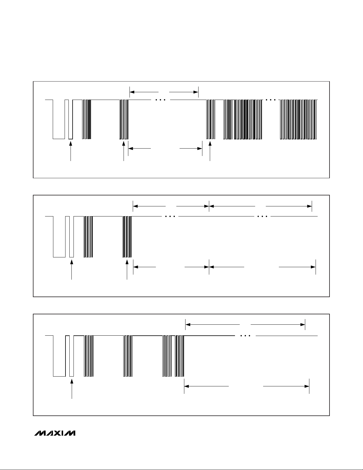
DS2775/DS2776/DS2777/DS2778
2-Cell, Stand-Alone, Li+ Fuel-Gauge IC with
Protector and Optional SHA-1 Authentication
______________________________________________________________________________________ 39
Figure 25. Compute MAC Command
1-Wire
RESET
SKIP-ROM
COMMAND
PRESENCE
PULSE
COMPUTE
NEXT SECRET COMMAND
WAIT FOR MAC
COMPUTATION
WAIT FOR EEPROM
PROGRAMMING
t
SHA
t
EEC
Figure 26. Compute Next Secret Command
1-Wire
RESET
SKIP-ROM
COMMAND
COPY DATA
COMMAND
8 WRITE
TIME SLOTS
PRESENCE
PULSE
WAIT FOR EEPROM
PROGRAMMING
t
EEC
Figure 27. Copy Data Command
t
SHA
1-Wire
RESET
PRESENCE
PULSE
SKIP-ROM
COMMAND
COMPUTE
MAC COMMAND
WAIT FOR MAC
COMPUTATION
UP TO 160 READ TIME SLOTS
(READ 20-BYTE MAC)
8 WRITE-ZERO
TIME SLOTS
Page 40

DS2775/DS2776/DS2777/DS2778
2-Cell, Stand-Alone, Li+ Fuel-Gauge IC with
Protector and Optional SHA-1 Authentication
40 ______________________________________________________________________________________
1-Wire Signaling
The 1-Wire bus requires strict signaling protocols to
ensure data integrity. The four protocols used by the
DS2775/DS2776 are as follows: the initialization
sequence (reset pulse followed by presence pulse),
write-zero, write-one, and read data. The bus master
initiates all these types of signaling except the presence pulse.
Figure 29 shows the initialization sequence required to
begin any communication with the DS2775/DS2776. A
presence pulse following a reset pulse indicates that
the DS2775/DS2776 are ready to accept a Net Address
command. The bus master transmits (Tx) a reset pulse
for t
RSTL
. The bus master then releases the line and
goes into receive mode (Rx). The 1-Wire bus line is
then pulled high by the pullup resistor. After detecting
the rising edge on the DQ pin, the DS2775/DS2776 wait
for t
PDH
and then transmit the presence pulse for t
PDL
.
1-Wire
RESET
SKIP-ROM
COMMAND
CLEAR/LOCK
SECRET COMMAND
OR SET/CLEAR
OVERDRIVE COMMAND
PRESENCE
PULSE
WAIT FOR EEPROM
COPY TIME
t
EEC
Figure 28. Clear/Lock Secret, Set/Clear Overdrive Commands
RESISTOR PULLUP
BUS MASTER ACTIVE LOW
LINE TYPE LEGEND:
DQ
DS2775/DS2776 ACTIVE LOW
PK+
PK-
t
RSTL
t
RSTH
t
PDL
t
PDH
Figure 29. 1-Wire Initialization Sequence
Page 41

DS2775/DS2776/DS2777/DS2778
2-Cell, Stand-Alone, Li+ Fuel-Gauge IC with
Protector and Optional SHA-1 Authentication
______________________________________________________________________________________ 41
Write Time Slots
A write time slot is initiated when the bus master pulls
the 1-Wire bus from a logic-high (inactive) level to a
logic-low level. There are two types of write time slots:
write-one and write-zero. All write time slots must be
t
SLOT
in duration with a 1µs minimum recovery time,
t
REC
, between cycles. The DS2775/DS2776 sample the
1-Wire bus line between t
LOW1_MAX
and t
LOW0_MIN
after the line falls. If the line is high when sampled, a
write-one occurs. If the line is low when sampled, a
write-zero occurs. Figure 30 illustrates the sample window. For the bus master to generate a write-one time
slot, the bus line must be pulled low and then released,
allowing the line to be pulled high less than t
RDV
after
the start of the write time slot. For the host to generate a
write-zero time slot, the bus line must be pulled low and
held low for the duration of the write time slot.
Read Time Slots
A read time slot is initiated when the bus master pulls the
1-Wire bus line from a logic-high level to a logic-low
level. The bus master must keep the bus line low for at
least 1µs and then release it to allow the DS2775/
DS2776 to present valid data. The bus master can then
sample the data t
RDV
from the start of the read time slot.
By the end of the read time slot, the DS2775/DS2776
release the bus line and allow it to be pulled high by the
external pullup resistor. All read time slots must be t
SLOT
in duration with a 1µs minimum recovery time, t
REC
,
between cycles. See Figure 30 and the timing specifications in the
Electrical Characteristics: 1-Wire Interface,
Standard/Overdrive
tables for more information.
2-Wire Bus System
The 2-wire bus system supports operation as a slaveonly device in a single or multislave and single or multimaster system. Up to 128 slave devices can share the
bus by uniquely setting the 7-bit slave address. The
2-wire interface consists of a serial data line (SDA) and
serial clock line (SCL). SDA and SCL provide bidirectional communication between the DS2777/DS2778
slave device and a master device at speeds up to
400kHz. The DS2777/DS2778’s SDA pin operates bidirectionally, that is, when the DS2777/DS2778 receive
data, SDA operates as an input, and when the
DS2777/DS2778 return data, SDA operates as an opendrain output with the host system providing a resistive
pullup. The DS2777/DS2778 always operate as a slave
device, receiving and transmitting data under the con-
trol of a master device. The master initiates all transactions on the bus and generates the SCL signal as well
as the START and STOP bits which begin and end
each transaction.
Bit Transfer
One data bit is transferred during each SCL clock cycle
with the cycle defined by SCL transitioning low-to-high
and then high-to-low. The SDA logic level must remain
stable during the high period of the SCL clock pulse.
Any change in SDA when SCL is high is interpreted as
a START (S) or STOP (P) control signal.
Bus Idle
The bus is defined to be idle, or not busy, when no
master device has control. Both SDA and SCL remain
high when the bus is idle. The STOP condition is the
proper method to return the bus to the idle state.
START and STOP Conditions
The master initiates transactions with a START condition by forcing a high-to-low transition on SDA while
SCL is high. The master terminates a transaction with a
STOP condition, a low-to-high transition on SDA while
SCL is high. A repeated START condition (Sr) can be
used in place of a STOP then START sequence to terminate one transaction and begin another without
returning the bus to the idle state. In multimaster systems, a repeated START allows the master to retain
control of the bus. The START and STOP conditions are
the only bus activities in which the SDA transitions
when SCL is high.
Acknowledge Bits
Each byte of a data transfer is acknowledged with an
acknowledge bit (A) or a not acknowledge bit (N). Both
the master and the DS2777/DS2778 slave generate
acknowledge bits. To generate an acknowledge, the
receiving device must pull SDA low before the rising
edge of the acknowledge-related clock pulse (9th
pulse) and keep it low until SCL returns low. To generate a not acknowledge (also called NACK), the receiver
releases SDA before the rising edge of the acknowledge-related clock pulse and leaves SDA high until
SCL returns low. Monitoring the acknowledge bits
allows for detection of unsuccessful data transfers. An
unsuccessful data transfer can occur if a receiving
device is busy or if a system fault has occurred. In the
event of an unsuccessful data transfer, the bus master
should reattempt communication.
Page 42
DS2775/DS2776/DS2777/DS2778
2-Cell, Stand-Alone, Li+ Fuel-Gauge IC with
Protector and Optional SHA-1 Authentication
42 ______________________________________________________________________________________
Figure 30. 1-Wire Write and Read Time Slots
WRITE-ZERO SLOT WRITE-ONE SLOT
V
PULLUP
GND
MODE:
STANDARD
t
SLOT
t
LOW0
t
REC
DEVICE SAMPLE WINDOW
MIN TYP MAX
15μs 30μs15μs
30μs15μs
> 1μs
t
LOW1
MIN TYP MAX
t
SLOT
DEVICE SAMPLE WINDOW
15μs
t
SLOT
3μs2μs
t
REC
t
RDV
OVERDRIVE
V
PULLUP
GND
1μs
READ-ZERO SLOT READ-ONE SLOT
t
RDV
> 1μs
MODE:
STANDARD
OVERDRIVE
15μs
2μs
LINE TYPE LEGEND:
MASTER SAMPLE WINDOW MASTER SAMPLE WINDOW
15μs
2μs
BUS MASTER ACTIVE LOW
BOTH BUS MASTER AND
SLAVE ACTIVE LOW
SLAVE ACTIVE LOW
RESISTOR PULLUP
t
3μs2μs 1μs
SLOT
Page 43

DS2775/DS2776/DS2777/DS2778
2-Cell, Stand-Alone, Li+ Fuel-Gauge IC with
Protector and Optional SHA-1 Authentication
______________________________________________________________________________________ 43
Data Order
A byte of data consists of 8 bits ordered MSb first. The
LSb of each byte is followed by the acknowledge bit.
The DS2777/DS2778 registers composed of multibyte
values are ordered MSB first. The MSB of multibyte registers is stored on even data memory addresses.
Slave Address
A bus master initiates communication with a slave
device by issuing a START condition followed by a
slave address (SAddr) and the read/write (R/W) bit.
When the bus is idle, the DS2777/DS2778 continuously
monitor for a START condition followed by its slave
address. When the DS2777/DS2778 receive a slave
address that matches the value in its Programmable
Slave Address register, they respond with an acknowledge bit during the clock period following the R/W bit.
The 7-bit Programmable Slave Address register is factory programmed to 1011001. The slave address can
be reprogrammed. See the
Programmable Slave
Address
section for details.
Programmable Slave Address
The 2-wire slave address of the DS2777/DS2778 is
stored in the parameter EEPROM block, address 80h.
Programming the slave address requires a write to 80h
with the desired slave address. The new slave address
value is effective following the write to 80h and must be
used to address the DS2777/DS2778 on subsequent
bus transactions. The slave address value is not stored
to EEPROM until a Copy EEPROM Block 1 command is
executed. Prior to executing the Copy Data command,
power cycling the DS2777/DS2778 restores the original
slave address value. The data format of the slave
address value in address 80h is shown in the
Slave
Address Format (80h)
section.
Read/Write Bit
The R/W bit following the slave address determines the
data direction of subsequent bytes in the transfer. R/W
= 0 selects a write transaction, with the subsequent
bytes being written by the master to the slave. R/W = 1
selects a read transaction, with the subsequent bytes
being read from the slave by the master.
Bus Timing
The DS2777/DS2778 are compatible with any bus timing up to 400kHz. No special configuration is required
to operate at any speed.
2-Wire Command Protocols
The command protocols involve several transaction formats. The simplest format consists of the master writing
the START bit, slave address, R/W bit, and then monitoring the acknowledge bit for presence of the
DS2777/DS2778. More complex formats such as the
Write Data, Read Data, and function command protocols write data, read data, and execute device-specific
operations. All bytes in each command format require
the slave or host to return an acknowledge bit before
continuing with the next byte. Each function command
definition outlines the required transaction format. Table
14 applies to the transaction formats.
Basic Transaction Formats
Write: S SAddr W A MAddr A Data0 A P
A write transaction transfers one or more data bytes to
the DS2777/DS2778. The data transfer begins at the
memory address supplied in the MAddr byte. Control of
the SDA signal is retained by the master throughout the
transaction, except for the acknowledge cycles.
A read transaction transfers one or more bytes
from
the
DS2777/DS2778. Read transactions are composed of
two parts with a write portion followed by a read portion
and are, therefore, inherently longer than a write transaction. The write portion communicates the starting
point for the read operation. The read portion follows
immediately, beginning with a repeated START, and
slave address with R/W set to a 1. Control of SDA is
Slave Address Format (80h)
Bits 7 to 1: Slave Address (A[6:0]). A[6:0] contains the 7-bit slave address of the DS2777/DS2778. The factory
default is 1011001b.
Bit 0: Reserved.
Read: S SAddr W A MAddr A Sr SAddr R A Data0 N P
Write Portion Read Portion
BIT 7 BIT 6 BIT 5 BIT 4 BIT 3 BIT 2 BIT 1 BIT 0
A6 A5 A4 A3 A2 A1 A0 X
Page 44
DS2775/DS2776/DS2777/DS2778
2-Cell, Stand-Alone, Li+ Fuel-Gauge IC with
Protector and Optional SHA-1 Authentication
44 ______________________________________________________________________________________
Table 14. 2-Wire Protocol Key
assumed by the DS2777/DS2778 beginning with the
slave address acknowledge cycle. Control of the SDA
signal is retained by the DS2777/DS2778 throughout
the transaction, except for the acknowledge cycles.
The master indicates the end of a read transaction by
responding to the last byte it requires with a no
acknowledge. This signals the DS2777/DS2778 that
control of SDA is to remain with the master following the
acknowledge clock.
Write-Data Protocol
The write-data protocol is used to write to register and
shadow RAM data to the DS2777/DS2778 starting at
memory address MAddr. Data0 represents the data
written to MAddr, Data1 represents the data written to
MAddr + 1 and DataN represents the last data byte,
written to MAddr + N. The master indicates the end of a
write transaction by sending a STOP or repeated
START after receiving the last acknowledge bit.
S SAddr W A MAddr A Data0 A Data1 A … DataN A P
The MSb of the data to be stored at address MAddr
can be written immediately after the MAddr byte is
acknowledged. Because the address is automatically
incremented after the LSb of each byte is received by
the DS2777/DS2778, the MSb of the data at address
MAddr + 1 is written immediately after the acknowledgement of the data at address MAddr. If the bus
master continues an autoincremented write transaction
beyond address 4Fh, the DS2777/DS2778 ignore the
data. Data is also ignored on writes to read-only
addresses and reserved addresses, locked EEPROM
blocks, as well as a write that auto-increments to the
Function Command register (address FEh). Incomplete
bytes and bytes that are not acknowledged by the
DS2777/DS2778 are not written to memory. As noted in
the
Memory
section, writes to unlocked EEPROM
blocks modify the shadow RAM only.
Read-Data Protocol
The read-data protocol is used to read register and
shadow RAM data from the DS2777/DS2778 starting at
a memory address specified by MAddr. Data0 represents the data byte in memory location MAddr, Data1
represents the data from MAddr + 1, and DataN represents the last byte read by the master.
S SAddr W A MAddr A Sr SAddr R A Data0 A Data1 A
… DataN N P
Data is returned beginning with the MSb of the data in
MAddr. Because the address is automatically incremented after the LSb of each byte is returned, the MSb
of the data at address MAddr + 1 is available to the
host immediately after the acknowledgement of the
data at address MAddr. If the bus master continues to
read beyond address FFh, the DS2777/DS2778 output
data values of FFh. Addresses labeled reserved in the
Memory Map
return undefined data. The bus master
terminates the read transaction at any byte boundary
by issuing a not acknowledge followed by a STOP or
repeated START.
Function Command Protocol
The function command protocol executes a devicespecific operation by writing one of the function command values (FCmd) to memory address FEh. Table 15
lists the DS2777/DS2778 FCmd values and describes
the actions taken by each. A 1-byte write protocol is
used to transmit the function command, with the MAddr
set to FEh and the data byte set to the desired FCmd
value. Additional data bytes are ignored. Data read
from memory address FEh is undefined.
S SAddr W A MAddr = 0FEh A FCmd A P
KEY DESCRIPTION KEY DESCRIPTION
S START Bit Sr Repeated START
SAddr Slave Address (7-bit) W R/W Bit = 0
FCmd Function Command Byte R R/W Bit = 1
MAddr Memory Address B yte P STOP bit
Data Data Byte Written by Master Data Data Byte Returned by Slave
A Acknowledge Bit (Master) A Acknowledge Bit (Slave)
N Not Acknowledge (Master) N Not Acknow ledge (Slave)
Page 45
DS2775/DS2776/DS2777/DS2778
2-Cell, Stand-Alone, Li+ Fuel-Gauge IC with
Protector and Optional SHA-1 Authentication
______________________________________________________________________________________ 45
Table 15. Function Commands
Selector Guide
PART INTERFACE SHA-1
DS2775G+ 1-Wire No
DS2775G+T& R 1-Wire No
DS2776G+ 1-Wire Yes
DS2776G+T& R 1-Wire Yes
DS2777G+ 2-Wire No
DS2777G+T& R 2-Wire No
DS2778G+ 2-Wire Yes
DS2778G+T& R 2-Wire Yes
+
Denotes a lead(Pb)-free/RoHS-compliant package.
T&R = Tape and reel.
PACKAGE
TYPE
PACKAGE
CODE
OUTLINE
NO.
LAND
PATTERN NO.
14 TDFN-EP T1435N+1
21-0253 90-0246
Package Information
For the latest package outline information and land patterns
(footprints), go to www.maxim-ic.com/packages
. Note that a
“+”, “#”, or “-” in the package code indicates RoHS status only.
Package drawings may show a different suffix character, but
the drawing pertains to the package regardless of RoHS status.
FUNCTION
COMMAND
Copy Data
Recall Data
Lock
Read ROM
ID
TARGET
EEPROM
BLOCK
0 42h
1 44h
0 B2h
1 B4h
0 63h
1 66h
— 39h
FCmd
VALUE
DESCRIPTION
Thi s command copies the shadow RAM to the target EEPROM block. Copy data
commands that target locked blocks are ignored. While the Copy Data command is
executing, the EEC bit in the EEPROM register is set to 1, and write data commands
with MAddr set to any address within the target block are ignored. Read data and
write data commands with MAddr set outside the target block are processed while
the copy is in progress. The Copy Data command execution time, t
typical and starts after the FCmd byte i s acknowledged. Subsequent copy or lock
commands must be delayed until the EEPROM programming cyc le completes.
Thi s command recalls the contents of the targeted EEPROM block to its shadow
RAM.
Thi s command locks (write protects) the targeted EEPROM block. The LOCK bit in
the EEPROM register must be set to 1 before the Lock command is executed. If the
LOCK bit is 0, the Lock command has no effect. The Lock command is permanent;
a locked block can never be written again. The Lock command execution time,
t
, is 2ms t ypical and starts after the FCmd byte is acknowledged. Subsequent
EEC
copy or loc k commands must be dela yed until the EEPROM programming cycle
completes.
Thi s command initiates a read of the unique 64-bit ROM ID. After the Read ROM ID
command is sent, the ROM ID can be read with the following sequence:
S SAddr R Data0 A Data1 A ... Data7 N P.
EEC
, is 2ms
Page 46
Revision History
Maxim cannot assume responsibility for use of any circuitry other than circuitry entirely embodied in a Maxim product. No circuit patent licenses are
implied. Maxim reserves the right to change the circuitry and specifications without notice at any time.
46
____________________Maxim Integrated Products, 120 San Gabriel Drive, Sunnyvale, CA 94086 408-737-7600
© 2011 Maxim Integrated Products Maxim is a registered trademark of Maxim Integrated Products, Inc.
2-Cell, Stand-Alone, Li+ Fuel-Gauge IC with
Protector and Optional SHA-1 Authentication
DS2775/DS2776/DS2777/DS2778
REVISION
NUMBER
0 10/08 Initial release —
1 3/09 Corrected values in the VOV Register Programmab il it y table (Table 5) 27
2 7/09 Corrected the 2-wire slave address default value to 1011001 42
3 5/10 Clarified ESD sensitivity to avo id confu sion
4 6/11
REVISION
DATE
DESCRIPTION
Updated the DS2775/DS2776 Typical Application Circuit and DS2777/DS2778
Typical Application Circuit; corrected the product family code from 32h to 3Dh in
the 64-Bit Net Address ( ROM ID) section and Figure 22
PAGES
CHANGED
2, 7, 11, 13,
24, 25, 45
10, 33
 Loading...