

r
www.maxim-ic.com
GENERAL DESCRIPTION
The DS2714 is ideal for standalone charging of 1 to 4
AA or AAA NiMH “loose” cells. NiCd cells can also be
charged. Temperature, voltage and charge time are
monitored to provide proper fast charging control
algorithms for Nickel Metal Hydride (NiMH) batteries.
Battery tests are included to detect defective or
inappropriate cells such as Alkaline primary batteries.
The DS2714 supports a parallel charging topology,
with independent monitoring and control of each cell.
APPLICATIONS
Desktop/Standalone Chargers (AAA/AA)
Digital Still Cameras
Music Players
Games
Toys
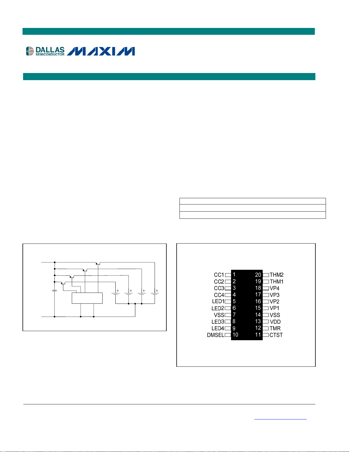
CHARGE TOPOLOGY
DS2714
Quad Loose Cell NiMH Charge
FEATURES
Charges 1 to 4 NiMH Cells
Detects and Avoids Charging Alkaline Cells
Pre-Charges Deeply Depleted Cells
Fast Charges NiMH with -ΔV Termination
Sensitivity of 2mV (typ)
Monitors Voltage, Temperature and Time for
Safety and Secondary Termination
Works with Regulated Charge Current Source
Drives PNP Type Pass Element
Compatible with Integrated Primary-Side PWM
Controllers
20-pin TSSOP Package
ORDERING INFORMATION
PART MARKING PIN-PACKAGE
DS2714E+ DS2714 20 TSSOP
DS2714E+T&R DS2714 20 TSSOP Tape-and-Reel
+Denotes lead-free package.
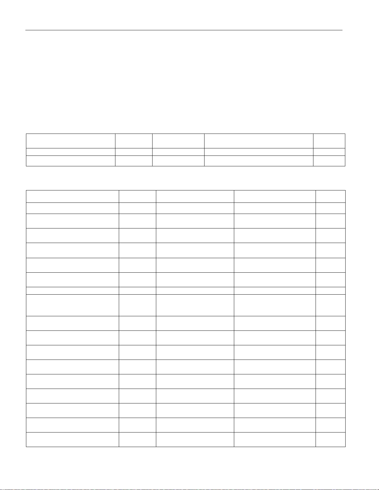
PIN CONFIGURATION
Controlled
Current
Source
GND
4-Cell NiMH Charger
DS2714
TSSOP
Note: Some revisions of this device may incorporate deviations from published specifications known as errata. Multiple revisions of any device
may be simultaneously available through various sales channels. For information about device errata, click here: www.maxim-ic.com/errata
1 of 12
REV: 080206
.
DS2714: Quad Loose Cell NiMH Charger
ABSOLUTE MAXIMUM RATINGS
Voltage Range on Any Pin Relative to V
Voltage on DMSEL V
Continuous Sink Current CC1-4, LED1-4
Operating Temperature Range -40°C to +85°C
Storage Temperature Range
Soldering Temperature
Stresses beyond those listed under “Absolute Maximum Ratings” may cause permanent damage to the device. These are stress ratings only,
and functional operation of the device at these or any other conditions beyond those indicated in the operational sections of the specifications is
not implied. Exposure to the absolute maximum rating conditions for extended periods may affect device reliability.
-55°C to +125°C
See IPC/JEDECJ-STD-020A
-0.3V to +6V
SS
+ 0.3V
DD
20mA
RECOMMENDED DC OPERATING CONDITIONS
(4.0V ≤ VDD ≤ 5.5V; T
PARAMETER SYMBOL CONDITIONS MIN TYP MAX UNITS
Supply Voltage VDD (Note 1) 4.0 5.5 V
Input Voltage Range LEDx, DMSEL -0.3 5.5 V
= -20°C to +70°C)
A
DC ELECTRICAL CHARACTERISTICS
(4.0V ≤ VDD ≤ 5.5V; TA = -20°C to +70°C. Unless otherwise noted.)
PARAMETER SYMBOL CONDITIONS MIN TYP MAX UNITS
Supply Current, VDD I
Output Voltage Low, CC1-4.
LED1-4
Leakage Current,
CC1-4 LED1-4
Threshold Voltage,
-ΔV Termination
Mode Test Current, DMSEL I
Input Logic High, DMSEL, VIH (Note 1)
Operating mode 500 750
DD
VDD = 5.0V,
V
OL1
I
LKG
V
MTST
-ΔV
= 20mA (Note 1)
I
OL
VDD = 5.0V,
Output inactive
After t
THO
Pulse high/low once
<5ms after power-up
1.0 2.0 3.0 mV
1.0 V
-1 +1
- 5 15
V
-
DD
0.2V
V
μA
μA
μA
Input Logic Low, DMSEL, VIL (Note 1) 0.2 V
Input Leakage Current,
DMSEL
Threshold Voltage, Cell Test
Accuracy
Threshold Voltage, Cell Test
Range
Threshold Voltage, Cell
Voltage Low
Threshold Voltage, Cell
Voltage Max1
Threshold Voltage, Cell
Voltage Max2
Threshold Voltage, Thermistor
- Min
Threshold Voltage, Thermistor
- Max
Threshold Voltage, Thermistor
- Stop
Threshold Current, TMR Pin
Suspend
I
IL1
V
CTST-ACC
V
CTST-RANGE
V
BAT-LOW
V
BAT-MAX1
V
BAT-MAX2
V
THM-MIN
V
THM-MAX
V
THM-STOP
I
TMR-SUS
After power-up mode
select,
DMSEL = V
R
= 80KΩ
TMR
or VSS
DD
-1 +1
μA
-15 15 %
32 400 mV
CC1 = CC2 = hi-Z
(Note 1, 2)
CC1 = CC2 = hi-Z
(Note 1, 2)
CC1, CC2 active
(Note 1, 2)
(Note 1, 2, 6)
(Note 1, 2, 6) 0.30
(Note 1, 2, 6)
0.1 0.5
0.9 1.0 1.1 V
1.55 1.65 1.75 V
1.64 1.75 1.86 V
V
x
DD
0.73
V
DD
0.33
V
DD
0.29
x
x
V
0.36 V
V
μA
2 of 12
DS2714: Quad Loose Cell NiMH Charger
PARAMETER SYMBOL CONDITIONS MIN TYP MAX UNITS
Presence Test Current, VP1-4 I
Reverse Leakage Current,
VP1, VP2, VP3, VP4
10 15
PTST
VDD = 0V, VPx = 1.5V
I
LKGR
2
μA
μA
ELECTRICAL CHARACTERISTICS: TIMING
(4.0V ≤ VDD ≤ 5.5V; TA = -20°C to +70°C. Unless otherwise noted.)
PARAMETER SYMBOL CONDITIONS MIN TYP MAX UNITS
Internal Timebase Period t
Internal Timebase
Accuracy
Duty Factor, Fast Charge DF1 CCx 0.234
(Note 5) 0.48 s
BASE
-10 +10 %
Duty Factor, PreCharge/Top-Off
Duty Factor, Maintenance
Charge
Cell Test Interval t
Pre-Charge Time-out t
Fast Charge Termination
Hold-Off Period
Fast Charge Flat Voltage
Time-out
DF2 CCx 0.0625
DF3 CCx Note 4 0.0078
(Note 3) 31 s
CTST
V
PCHG
t
3.6 4 4.4 minutes
THO
V
t
FLAT
< V
CELL
not increasing 14.4 16 17.6 minutes
CELL
30.6 34 37.4 minutes
BAT-MIN
Charge Timer Accuracy -5 +5 %
Charge Timer Range t
CTMR-RANGE
0.5 10 h
Note 1: Voltages relative to V
Note 2: Specification applicable during charge cycle with TA = 0°C to +70°C.
Note 3: One time slot out of every 16 available slots gets a Cell Test.
Note 4: One time slot out of every 32 available time slots gets a charge pulse.
0.48 seconds is one charge time slot. A complete cycle of 4 time slots (one charge time slot per cell) is 1.92 sec.
Note 5:
Note 6: V
Note 7: I
THM-MIN, VTHM-MAX, and VTHM-STOP are fixed ratios of V
MTST current is applied as a source current and as a sink current within 5ms after power-up.
.
SS
Their ranges never overlap.
.
DD
3 of 12
DS2714: Quad Loose Cell NiMH Charger
PIN DESCRIPTION
PIN NAME FUNCTION
1 CC1
2 CC2
3 CC3
4 CC4
5 LED1
6 LED2
7 VSS
8 LED3
9 LED4
10 DMSEL
11 CTST
12 TMR
13 VDD
14 VSS
15 VP1
16 VP2
17 VP3
18 VP4
19 THM1
20 THM2
Charge Control 1. Turn on and off the charge PNP for Cell 1.
Charge Control 2. Turn on and off the charge PNP for Cell 2.
Charge Control 3. Turn on and off the charge PNP for Cell 3.
Charge Control 4. Turn on and off the charge PNP for Cell 4.
LED 1. Open drain output for LED. Display Cell 1 status.
LED 2. Open drain output for LED. Display Cell 2 status.
Device Ground. Return current path for LEDx pins. Both VSS pins must be connected to ground.
LED 3. Open drain output for LED. Display Cell 3 status.
LED 4. Open drain output for LED. Display Cell 4 status.
Display Mode Select. Select the LED blink rate.
Cell Test Resistor. Cell test threshold set.
Timer Resistor. Charge timer set.
Power-Supply Input. Chip supply input (4.0V to 5.5V).
Device Ground. Internally connected to Pin 7. Both VSS pins must be connected to ground.
Voltage Sense 1. Positive terminal sense input for Cell 1.
Voltage Sense 2. Positive terminal sense input for Cell 2.
Voltage Sense 3. Positive terminal sense input for Cell 3.
Voltage Sense 4. Positive terminal sense input for Cell 4.
Thermister 1. Thermister input for Cell 1 and 2.
Thermister 2. Thermister input for Cell 3 and 4.
4 of 12

Figure 1. Block Diagram
DS2714: Quad Loose Cell NiMH Charger
5 of 12

Figure 2. State Diagram
DS2714: Quad Loose Cell NiMH Charger
6 of 12

DS2714: Quad Loose Cell NiMH Charger
Figure 3. Application Example: Regulated Current Source Charger
7 of 12

DS2714: Quad Loose Cell NiMH Charger
DETAILED DESCRIPTION
CHARGE ALGORITHM OVERVIEW
A charge cycle begins in one of three ways: With the application of power to the DS2714 with cell(s) already
inserted, with the detection of cell insertion after power-up, or when exiting suspend mode with cell(s) inserted. The
charge cycle begins with Pre-charge qualification to prevent Fast charging of deeply depleted cells or charging
under extreme temperature conditions. Pre-charging is performed at a reduced rate until the cell being charged
reaches V
charging of alkaline cells or NiMH cells which are worn-out or damaged. Fast charging continues as long as the cell
temperature is less than 50°C (based on Thermistor sensors THM 1, 2), the open circuit cell voltage(s) are
between V
Fast charging terminates by the -ΔV (negative delta voltage) or flat voltage method. The Top-Off charge phase
follows to completely charge the cell. After the Top-off charge timer expires, the Maintenance charge phase
continues indefinitely to keep the cells fully charged. Maximum voltage, temperature and charge time monitoring
during all charge phases act as secondary or safety termination methods to provide additional protection from
overcharge. A cell voltage greater than V
than 50°C (see Table 1) will result in either Fault or Maintenance depending on which charge state the device was
last in. Each cell is monitored independently, and the charge phase of each cell is independently controlled. If a cell
is removed while being charged, the algorithm for that cell slot is completely reset to its Presence Test state without
affecting the charge control states of the other cells.
CHARGE CONFIGURATION
The DS2714 supports four slot standalone chargers. It alternates charge to the four slots every two seconds, with
one half second available to each cell. Removal or insertion of a cell into the charger does not disturb the charge
timing or charge rates of the other cells. Charge pulses are fed alternately to each cell under the control of the CCx
pins so that the charge regimes occur in parallel. The duty cycle on the CCx pins are completely independent of
one another. Transitions from Pre-charge to Fast charge, Fast charge to Top-off and Top-off to Maintenance occur
independently for each cell. The configuration shown in Figure 3 is for charging four cells with a current limited
source of 2A. The effective average fast charge current for each cell is 2A x 0.25 x 15/16 = 0.469A. The 15/16 term
is due to the fact that every 16
current is delivered to the cell during that time. Mechanical design of the holders is required to prevent insertion of
more than one cell in each slot. The holder design should also prevent electrical contact with reverse polarity
insertion.
PERFORMANCE REQUIREMENTS OVER TEMPERATURE AND VOLTAGE
INTERNAL OSCILLATORS AND CLOCK GENERATION
An internal oscillator provides the main clock source used to generate timing signals for internal chip operation. The
pre-charge timer, hold-off timers, and duty factors for the charging operations are derived from this timebase. There
are two separate timers for the impedance test and Fast Charge/Topoff functions.
(1V). The algorithm proceeds to a Fast charge phase which includes cell tests to avoid accidental
BAT-LOW
BAT-LOW
(1.0V) and V
BAT-MAX1
(1.65V) and the closed ciruit cell voltage(s) are less than V
BAT-MAX2
th
charge time slot is used for negative delta-voltage and impedance testing. No
(1.75V) will result in a fault condition, and temperature greater
BAT-MAX2
Valid NiMH
Charge Range
Below Operating
Voltage Range
Low
Temperature
Range
High
Temperature
Range
Abs. Max
Operating
Range
(1.75V).
8 of 12

DS2714: Quad Loose Cell NiMH Charger
CHARGE TIMER
The Charge Timer monitors the duration of charge in Fast and Top-Off charge phases, and is reset at the
beginning of each phase. The time-out period is set with an external resistor connected from the TMR pin to V
SS
.
Resistors can be selected to support Fast charge time-out periods of 0.5 to 10 hours and Top-off charge time-out
periods of 0.25 to 5 hours. If the timer expires in Fast charge, the timer count is reset and charging proceeds to the
Top-Off charge phase. The Top-Off time-out period is half of the Fast charge time-out period. When the timer
expires in Top-Off, charging proceeds to the Maintenance phase. The programmed charge time approximately
follows the equation:
t = 1.5
R / 1000 (time in minutes)
*
SUSPEND
Suspension of charge activity is possible by floating the TMR pin. All CCx outputs become high-Z and the Charge
Timer stops. The state machine and all timers are reset to their Presence Test conditions.
TEMPERATURE SENSE
Connecting an external 10kΩ NTC thermistor between THM1 or THM2 (THMx) and VSS, and a 10kΩ bias resistor
between V
and THMx allows the DS2714 to sense temperature. In order to sense the temperature of the battery
DD
cells, locate the thermistor close to the body of the battery cell. The THM1 thermistor should be placed between
cells 1 and 2, and THM2 thermistor between cells 3 and 4. Alternatively, the thermistors can sense ambient
temperature by locating them away from the cells. THM1 and THM2 can be tied together to sense temperature
using a single thermistor and bias resistor. The temperature qualification function can be defeated by tying THMx
pins to a single resistor divider supplying a voltage between the Thermistor-Min and Thermistor-Max threshold
voltages.
MIN, MAX TEMPERATURE COMPARE
The voltage thresholds of the THMx inputs (V
45°C when using the recommended 10kΩ bias and 10kΩ thermistor. If Fast charging is in progress, and the
voltage on THMx reaches V
THM-STOP (TA
> 50°C), Fast charging stops and the maintenance phase begins. In Pre-
charge the device will transition to the Fault state if the voltage on THMx reaches V
THM-MIN
, V
THM-MAX
) are set to allow Fast charging to start if 0°C < TA <
THM-STOP
.
Table 1. THM1, THM2 Thresholds
TEMPERATURE
THM
THRESHOLD
MIN 0.73 27.04k 0°C 4°C
MAX 0.33 4.925k 45°C 42°C
STOP 0.29 4.085k 50°C 47°C
RATIO
OF VDD
THERMISTOR
RESISTANCE
Semitec
103AT-2
Fenwal
197-103LAG-A01
173-103LAF-301
CELL VOLTAGE MONITORING
Individual cell voltages are monitored for minimum and maximum values, using the V
threshold limits. Upon inserting a cell or power-up with cells inserted, cell voltages must be less than the V
MAX2
threshold before charging begins. The V
MAX1
BAT-LOW
threshold determines whether a Pre-charge cycle should
precede the Fast charge cycle, and when to transition from Pre-charge to Fast charge. Once Fast charging
commences, cell voltages are compared to the V
BAT-MAX2
threshold once every 2 seconds. The comparison occurs
while the charge control pin (CC1-4) controlling current to the cell is active (low). When the charge control pin is
active such that charge is applied to the cell, the cell voltage is referred to as the V
control pin is inactive, the cell voltage is referred to as the V
displayed if V
than V
BAT-MAX1
is greater than V
ON
BAT-MAX2
. Charging is also halted and a fault condition is entered if V
. While Fast charge is in progress, cell voltage measurements are stored and compared to future
voltage. Charging is halted and a Fault condition is
OFF
ON
measurements for charge termination and cell test purposes.
BAT-LOW
, V
BAT-MAX1
and V
BAT-
BAT-
voltage. When the charge
is greater
OFF
9 of 12

DS2714: Quad Loose Cell NiMH Charger
CELL TESTS
Two types of tests are performed to detect primary Alkaline and Lithium cells or defective NiMH or NiCd secondary
cells. The first test checks the absolute closed circuit cell voltage (V
in open circuit cell voltage (V
seconds. During fast charge, V
V
, the cell test fails. Cells are tested individually so that a single improper or defective cell can be detected
CTST
quickly. V
is set by the resistance from the CTST pin to ground. The nominal sensitivity of 100mV is set by
CTST
connecting an 80kΩ resistor between CTST and V
) and (VON). VON for each cell is compared to the V
OFF
ON
- V
of each cell is compared to the cell test threshold, V
OFF
. The impedance threshold can be set from 32mV to 400mV.
SS
), and the second test checks the difference
ON
BAT-MAX2
threshold once every 2
. If VON - V
CTST
OFF
>
The following formula approximates the setting for the impedance threshold
V
= 8000/R (value in volts)
CTST
-ΔV AND FLAT VOLTAGE TERMINATION
During Fast charge, -ΔV detection is performed by comparing successive voltage measurements for a drop of 2mV
in the cell voltage. A Hold-off period for -ΔV detection begins at the start of Fast charging and prevents false
termination in the first few minutes of the charge cycle. Once the hold-off period expires, cell voltage
measurements are acquired every 16th charge time slot (approximately 31 seconds, during the CCx off time).
When a newly acquired voltage measurement is greater than any previous one, the new value is retained as the
maximum value. When the cell voltage no longer increases, the maximum value is retained and compared against
subsequent values. If the cell voltage drops below the -ΔV threshold, V
the cell voltage remains flat such that the maximum value persists for a period of 16 minutes (t
, (2mV typ), Fast charging is terminated. If
-ΔV
), Fast charge
FLAT
terminates and Top-Off charging begins.
TOP-OFF, PRE-CHARGE AND MAINTENANCE
In Top-off and Pre-charge modes, the charger scales the cell current to 1/16 of the DC current set by the current
source, i.e, one charge pulse for every 16 main clock pulses, or one in four available time slots for a given cell. The
ratio of average Top-off/Pre-charge current to average fast charge current is 0.286. When the charge timer expires
in Top-Off, the charger enters Maintenance and delivers 1/128 of the DC charge source current to the cells (one
time slot in every 32 available to that cell). This is slightly more than 3% of the average DC Fast Charge current.
Maintenance charge remains continuous until power is removed, the cell(s) are removed or the DS2714 is cycled
into and out of suspend mode by floating the TMR pin.
CCx OUTPUTS
The CC1 through CC4 pins operate as open-drain outputs that drive active low to connect the charge source to the
NiMH cells. During charge, the behavior of these outputs depends on the charge states of the cells and on how
many cells have been installed.
FAST CHARGE
Referring to the application circuit shown in Figure 3, CC1 controls the PNP switch that gates current to the cell in
slot 1. CC2 controls the PNP switch that gates current to the cell in slot 2, and so on. During Fast charge, current is
gated to each slot sequentially, with charge pulses occurring in alternating time frames. The cell in one slot charges
while the others relax. Each cell skips a charge pulse every 16 of its allocated charge time slots (approximately
once every 31 seconds) to facilitate independent testing of the open and closed circuit cell voltages (V
respectively). Since the charge regime of each cell is independent, one cell may complete a charge phase before
the other without affecting the charging of the other cells. In the case of an improper or faulty cell (ex. alkaline)
being inserted along with proper cells (NiMH or NiCd), charging of the improper cell would be stopped, while the
proper cells will be charged to full.
and VON,
OFF
10 of 12

EXAMPLE TIMING DIAGRAM FOR THE DS2714
DS2714: Quad Loose Cell NiMH Charger
Note 1: Cell test time slot for Cell 2.
Note 2: Cell test time slot for Cell 3.
In this timing diagram, the pulses represent charge current into the individual cells. Cell 1 is in Precharge (the timing of Precharge is the same as Top-off). It
gets one charge pulse out of every four available times slots.
Cell 2 is in initially in Fast Charge and it transitions to Topoff charge during the N+7th time interval (Note 1)shown in the diagram.
Cell 3 is in Fast charge. Cell testing is performed during the interval marked Note 2. This cell is not ready to go into Top-off and it resumes Fast charge.
Cell 4 is in maintenance mode, one out of every 32 available time slots gets a charge pulse.
11 of 12

DS2714: Quad Loose Cell NiMH Charger
LEDx OUTPUTS, DISPLAY MODE SELECT
Open-drain outputs LEDx pull low to indicate charge status. When inactive, the outputs are high impedance. LED1
displays the status for the cell monitored by VP1, LED2 displays the status for the cell monitored by VP2 and so on.
The LED pins drive low in three “blink” patterns to annunciate the charge status. Table 2 summarizes the LED
operation in each display mode (DM0, DM1, DM2) for each charge condition.
Table 2. Display Patterns By Display Mode and Charge Activity
Display Mode Charge Activity
DM0
DM1
DM2
DMSEL pin No Battery
Low Hi-Z Low
Float Hi-Z Low Hi-Z
High Hi-Z
Pre/Fast/Top-off
Charging
0.80s Low
0.16s Hi-Z
Maintenance Fault
0.80s Low
0.16s Hi-Z
Low
0.48s Low
0.48s Hi-Z
0.16s Low
0.16s Hi-Z
0.16s Low
0.16s Hi-Z
PACKAGE INFORMATION
(The package drawing(s) in this data sheet may not reflect the most current specifications. For the latest package
outline information, go to www.maxim-ic.com/DallasPackInfo
.)
Maxim/Dallas Semiconductor cannot assume responsibility for use of any circuitry other than circuitry entirely embodied in a Maxim/Dallas Semiconductor product.
No circuit patent licenses are implied. Maxim/Dallas Semiconductor reserves the right to change the circuitry and specifications without notice at any time.
Maxim Integrated Products, 120 San Gabriel D rive, Sunnyvale, CA 94086 408-737-7600
The Maxim logo is a registered trademark of Maxim Integrated Products, Inc. The Dallas logo is a registered trademark of Dallas Semiconductor Corporation.
© 2006 Maxim Integrated Products • Printed USA
12 of 12
 Loading...