


Loose Cell NiMH Chargers
DS2711/DS2712
www.maxim-ic.com
DESCRIPTION
The DS2711 and DS2712 are ideal for in-system or
stand-alone charging of 1 or 2 AA or AAA NiMH
“loose” cells. Temperature, voltage, and charge time
are monitored to provide proper fast charging control
algorithms for nickel metal hydride (NiMH) batteries.
Battery tests are included to detect defective or
inappropriate cells such as alkaline primary batteries.
The DS2711/DS2712 support series and parallel
topologies, with independent monitoring and control of
each cell. Charging of NiCd chemistry cells is also
supported.
FEATURES
§ Charge 1 or 2 NiMH Cells
§ Detect and Avoid Charging Alkaline Cells
§ Precharge Deeply Depleted Cells
§ Fast Charge NiMH with -DV Termination
Sensitivity of 2mV (typ)
§ Monitor Voltage, Temperature, and Time for
Safety and Secondary Termination
§ Regulate Charge Current:
Linear Control (DS2711)
Switch-Mode Control (DS2712)
§ Drive PMOS or PNP-Type Pass Element or
Switch, or an Optocoupler
§ Compatible with Popular Optocouplers and
Integrated Primary Side PWM Controllers
§ Small 16-Pin SO or TSSOP Package
APPLICATIONS
Desktop/Stand-Alone Chargers (AAA/AA)
Digital Still Cameras
Music Players
Games
Toys
PIN CONFIGURATION
CC1
CC2
LED1
VSS
LED2
CSOUT
VN1
VN0
16 SO (150 mil) / TSSOP (4.4 mm)
See Table 1 for Ordering Information.
1
2
3
4
5
6
7
8
16
15
14
13
12
11
10
VP2
VP1
THM2
THM1
VDD
TMR
CTST
9
DMSEL
PIN DESCRIPTION
PIN NAME FUNCTION
1 CC1 Cell 1 Charge-Control Output
2 CC2 Cell 2 Charge-Control Output
3 LED1 Cell 1 Status
4 VSS
5 LED2 Cell 2 Status, Mode-Select Input
6 CSOUT Current-Sense Output
7 VN1 Current-Sense + Input
8 VN0 Current-Sense - Input
9 DMSEL Display-Mode Select
10 CTST Cell Test Threshold Set
11 TMR Charge Timer Set
12 VDD Chip-Supply Input (4.0V to 5.5V)
13 THM1 Cell 1 Thermistor Input
14 THM2 Cell 2 Thermistor Input
15 VP1 Cell 1 Positive-Terminal Sense Input
16 VP2 Cell 2 Positive-Terminal Sense Input
Ground Reference and Chip-Supply
Return
1 of 14 080905

DS2711/DS2712: Loose Cell NiMH Charger
Table 1. ORDERING INFORMATION
PART MARKING PIN-PACKAGE
DS2711Z
DS2711
16 SO
DS2711Z/T&R DS2711 16 SO, Tape-and-Reel
DS2712Z
DS2712
16 SO
DS2712Z/T&R DS2712 16 SO, Tape-and-Reel
DS2711Z+
DS2711
16 SO
DS2711Z+T&R DS2711 16 SO, Tape-and-Reel
DS2712Z+
DS2712
16 SO
DS2712Z+T&R DS2712 16 SO, Tape-and-Reel
DS2711E+
DS2711
16 TSSOP
DS2711E+T&R DS2711 16 TSSOP, Tape-and-Reel
DS2712E+
DS2712
16 TSSOP
DS2712E+T&R DS2712 16 TSSOP, Tape-and-Reel
+ Denotes lead-free package.
ABSOLUTE MAXIMUM RATINGS*
Voltage on All Pins Relative to VSS -0.3V to +6V
Voltage on DMSEL V
+ 0.3V
DD
Continuous Sink Current CC1, CC2, LED1, LED2 and CSOUT 20mA
Operating Temperature Range -40°C to +85°C
Storage Temperature Range -55°C to +125°C
Soldering Temperature See IPC/JEDECJ-STD-020
*This is a stress rating only and functional operation of the device at these or any other conditions above those
indicated in the operation sections of this specification is not implied. Exposure to absolute maximum rating
conditions for extended periods of time may affect reliability.
RECOMMENDED DC OPERATING CONDITIONS
(4.0V £ VDD £ 5.5V; TA = -20°C to +70°C.)
PARAMETER SYMBOL CONDITIONS MIN TYP MAX UNITS
Supply Voltage VDD (Note 1) 4.0 5.5 V
Input Voltage Range LED2, DMSEL -0.3 +5.5 V
DC ELECTRICAL CHARACTERISTICS
(4.0V £ VDD £ 5.5V, TA = -20°C to +70°C, unless otherwise noted.)
PARAMETER SYMBOL CONDITIONS MIN TYP MAX UNITS
Supply Current, VDD I
UVLO Threshold V
UVLO Hysteresis V
Output-Voltage Low,
CC1, CC2, LED1, LED2
Output-Voltage Low,
CSOUT
Leakage Current,
CC1, CC2, LED1, LED2,
CSOUT
Threshold Voltage,
-DV Termination
Mode Test Current,
DMSEL, LED2
Operating mode 250 500
DD
VDD rising (Note 1) 3.5 3.9 V
UVLO
falling from above
V
UHYS
V
OL1
V
OL2
I
LKG
V
-DV
I
(Notes 2, 3) 5 15
MTST
DD
V
UVLO
= 5.0V,
V
DD
= 20mA (Note 1)
I
OL
= 5.0V,
V
DD
I
= 20mA (Note 1)
OL
= 5.0V,
V
DD
Output inactive
After t
1.0 2.0 3.0 mV
THO
2 of 14
mA
40 mV
1.0 V
0.75 1.25 V
-1 +1
mA
mA
DS2711/DS2712: Loose Cell NiMH Charger
PARAMETER SYMBOL CONDITIONS MIN TYP MAX UNITS
Input Logic-High,
DMSEL, LED2
Input Logic-Low, DMSEL,
LED2
Input Leakage Current,
DMSEL
Threshold Voltage, Cell
Test
Threshold Voltage, Cell
Voltage Low
Threshold Voltage, Cell
Voltage Max1
Threshold Voltage, Cell
Voltage Max2
Threshold Voltage Delta V
Threshold Voltage,
Thermistor - Min
Threshold Voltage,
Thermistor - Max
Threshold Voltage,
Thermistor - Stop
Threshold Current, TMR
Pin Suspend
Presence Test Current,
VP1, VP2
Reverse Leakage
Current, VP1, VP2
V
(Note 1)
IH
V
(Note 1) 0.2 V
IL
After power-up mode
I
IL1
V
CTST
V
BAT-LOW
V
BAT-MAX1
V
BAT-MAX2
BAT-MAX∆
V
THM-MIN
V
THM-MAX
V
THM-STOP
I
TMR-SUS
I
PTST
I
LKGR
select,
- V
or VSS
DD
BAT-MAX1
DMSEL = V
= 80kW
R
CTST
CC1 = CC2 = high-Z
(Note 4)
CC1 = CC2 = high-Z
(Note 4)
CC1, CC2 active
(Note 4)
V
BAT-MAX2
(Note 5)
(Notes 1, 4, 6)
(Notes 1, 4, 6) 0.30
(Notes 1, 4, 6)
0.1 0.5
Parallel: V
Series: V
= 0V, VP1 = 1.5V,
V
DD
VP2 = 3.0V
≥ 4.0V,
DD
≥ 4.5V
DD
-
V
DD
0.2V
-1 +1
V
mA
85 100 115 mV
0.9 1.0 1.1 V
1.55 1.65 1.75 V
1.64 1.75 1.86 V
90 100 110 mV
x
V
DD
0.73
V
DD
0.33
V
DD
0.29
x
x
V
0.36 V
V
mA
10 15
2
mA
mA
Current-Sense Reference
Voltage
Gain, Current-Sense
Error Amp
Gain, Current-Sense
Comparator
Propagation Time,
Current-Sense
Comparator
Hysteresis, CurrentSense Comparator
V
(Note 1, 4, 7)
IREF
G
DS2711 (Note 8) 0.9 1.5
M
G
DS2712 (Note 8) 10
M
t
PDLY
V
HYS-COMP
DS2712, 2mV
over/underdrive
DS2712 22 24 26 mV
125 mV
-6% +6% %
-1
W
-1
W
0.25
ms
ELECTRICAL CHARACTERISTICS: TIMING
(4.0V £ VDD £ 5.5V, TA = -20°C to +70°C, unless otherwise noted.)
PARAMETER SYMBOL CONDITIONS MIN TYP MAX UNITS
Internal Timebase Period t
Internal Timebase
Accuracy
Duty Factor, Series Fast
Charge
Duty Factor, Series
Precharge/Top-Off
Duty Factor, Parallel Fast
Charge
0.96 s
BASE
-10 +10 %
CC1 0.969
CC1 0.250
CC1, CC2 0.484
3 of 14

DS2711/DS2712: Loose Cell NiMH Charger
PARAMETER SYMBOL CONDITIONS MIN TYP MAX UNITS
Duty Factor, Parallel
Precharge/Top-Off
Duty Factor, Maintenance
Charge
CC1, CC2 0.125
CC1, CC2 0.0156
Cell Test Interval t
Precharge Time-Out t
Fast-Charge Termination
Hold-Off Period
Fast-Charge Flat Voltage
Time-Out
Charge Timer Period t
PCHG
t
t
CTMR
Charge Timer Accuracy
Charge Timer Range t
Note 1:
Note 2:
Note 3:
Note 4:
Note 5:
Note 6:
Note 7:
Note 8:
Voltages relative to V
I
current is applied as a source current and as a sink current within 5ms after power-up.
MTST
When operating in two-cell-series charge configuration, the DMSEL pin must have less than 50pF of external load capacitance
for proper operation. If the load capacitance is greater than 50pF, a resistor voltage divider should be used to maintain DMSEL
/ 2.
at V
DD
Specification applicable during charge cycle with T
V
V
Tested with I
Gain tested with 1mV step with I
and V
BAT-MAX1
THM-MIN, VTHM-MAX,
BAT-MAX1
CSOUT
CTMR-RANGE
.
SS
are generated from the same reference. Their ranges never overlap.
and V
THM-STOP
= -1mA.
31 s
CTST
V
4 minutes
THO
V
FLAT
< V
CELL
not increasing 16 minutes
CELL
= 100kW
R
TMR
= 100kW
R
TMR
34 minutes
BAT-MIN
2.5 h
-5 +5 %
0.5 10 h
= 0°C to +70°C.
A
are fixed ratios of V
= -1mA.
CSOUT
Their ranges never overlap.
DD.
4 of 14

Figure 1. BLOCK DIAGRAM
DS2711/DS2712: Loose Cell NiMH Charger
VDD
CC1
CC2
LED1
LED2
DMSEL
CTST
TMR
3.7V
Cell
Test
Charge
Timer
Charge
Mod e
Sele ct
0.1V
BIAS
UVLO
Oscillator
State Machine
Presence Test
Pre-Charge
Fast Charge
Cell Tests
Top-Off Charge
Maintenance Charge
Watchdog
ABORT
I
PTST
I
PTST
VP1
Voltage
and
Temperature
Measurement
VP2
VN1
THM1
THM2
+
&
-
VN0
VSS
-
CSOUT
+
0.125V
DS2711
SUSPEND
+
DS2712
5 of 14

Figure 2. STATE DIAGRAM
R
V
t
R
V
R
R
t
f
t
R
t
R
t
R
V
V
V
k
t
V
VDD < VPOR -VHYS
(asynchronously from
anywhere)
PO
Standby power
CCx = Hi-Z
LEDx = Hi-Z
VDD > VPOR (3.7V)
Presence
TEST
CCx = Hi-Z
LEDx = No Battery
DS2711/DS2712: Loose Cell NiMH Charger
VBAT > 1.75
O
T < 0C
O
T > 45C
t < PCTimeou
O
VBAT < 1V
t < Fast Timeou
t < Topoff Timeout
VBAT > 1V
AND
t < PCTimeou
AND
T < 50C
CHG
CCx = Act ive
48% Par., 97% Ser.
LEDx = Charging
delta-V detec
t > Fast Timeou
Topof
CHG
CCx = Act ive
12.5% Par., 25% Ser.
LEDx = Charging
PreCHG
CCx = Act ive
12.5% Par., 25% Ser.
LEDx = Charging
PASS
Fast
O
t > PCTimeou
VBAT > 1.75
Cell Test
CCx = Hi-Z
LEDx = Charging
32 cloc
interval
t > Topoff Timeout
VBAT < 1.65
O
T > 50
OR
FAIL:
VON - VOFF > V
T > 50
O
VBAT > 1.75
FAULT
Standby power
CCx = Hi-Z
LEDx = Fault
CTST
VBAT > 1.75
T > 50
MAINT
CCx = Act ive 1/64
LEDx = Ma intenance
VBAT > 1.75
(asynchronously
from anywhere)
t < 1s
6 of 14

DS2711/DS2712: Loose Cell NiMH Charger
DETAILED DESCRIPTION
Charge Algorithm Overview
A charge cycle begins in one of three ways: with the application of power to the DS2711 with cell(s) already
inserted, with the detection of cell insertion after power-up, or when exiting suspend mode with cell(s) inserted. The
charge cycle begins with precharge qualification to prevent fast charging of deeply depleted cells or charging under
extreme temperature conditions. precharging is performed at a reduced rate until each cell reaches 1V. The
algorithm proceeds to a fast-charge phase, which includes cell tests to avoid accidental charging of alkaline cells or
NiMH cells that are worn-out or damaged. Fast charging continues as long as the cell temperature(s) are less than
50°C (based on THM1, THM2 voltages) and the open-circuit cell voltage(s) are between 1.0V and 1.75V. Fast
charging terminates by the -DV (negative delta voltage) method. The top-off charge phase follows to completely
charge the cells. After the top-off charge timer expires, the maintenance charge phase continues indefinitely to
keep the cells at a full state of charge. Maximum voltage, temperature, and charge-time monitoring during all
charge phases act as secondary or safety termination methods to provide additional protection from overcharge.
Each cell is monitored independently, and in parallel mode the charge phase of each cell is independently
controlled.
Series Charge Configuration
The DS2711/DS2712 series configuration supports one or two-slot stand-alone and one or two cell in-system
chargers. The single-cell-series mode charges one cell while the two-cell-series mode charges two series cells.
Since the cells are charged in series, cell sizes should not be mixed in the series configuration. In the application
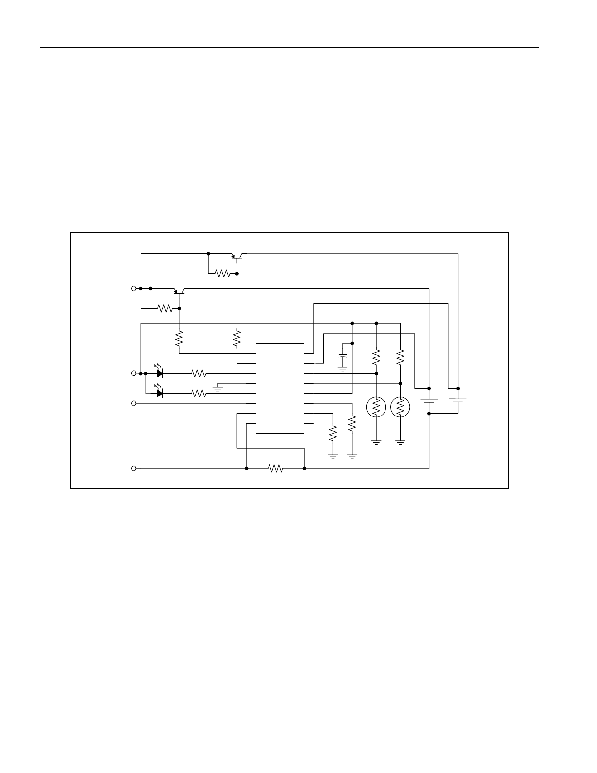
example in Figure 3, charge current is gated to the battery cells by a PNP transistor under the control of the CC1
pin of the DS2711. Current regulation is performed outside of this example schematic using the current-sense
feedback provided by the DS2711 CSOUT pin. The DS2712 can also be used in this circuit to provide switch-mode
control on the CSOUT pin. RSNS = 0.125W sets the charge source current, ICHG, to 1A. In series mode, the
effective charge current is 0.969 x ICHG = 969mA.
Figure 3. SERIES CONFIGURATION WITH EXTERNAL CURRENT
REGULATION
ICHG
+5V
IFB
GND
10K
FCX718
270
100
DS2711/12
CC1
CC2
LED1
VSS
LED2
VN1
VN0
RSNS
0.125
VP2
VP1
THM2
THM1
VDD
TMRCSOUT
CTST
DMSEL
75K
0.1
100K
10K
x2
103AT-2
x2
7 of 14
DS2711/DS2712: Loose Cell NiMH Charger
Parallel Charge Configuration
The parallel configuration supports two slot stand-alone chargers. Charge pulses are fed alternately to each cell
under the control of the CC1 and CC2 pins so the charge regimes occur in parallel. The duty cycle on CC1 and
CC2 are independent of one another. Transitions from precharge to fast charge, fast charge to top-off, and top-off
to maintenance occur independently for each cell.
The configuration shown in Figure 4 is for charging two cells with the current-sense feedback regulating the charge
source to 2A (RSNS = 0.068W). The effective charge current for each cell is 2A x 0.484 = 0.968A. A charger with
battery holders designed to accept either AA or AAA cell sizes can be constructed with the current-sense
resistance split between two separate resistors so each cell type (AA or AAA) is charged at a different rate.
Mechanical design of the holders is required to prevent insertion of more than one cell in each slot. The holder
design must also prevent electrical contact with reverse polarity insertion.
Figure 4. PARALLEL CONFIGURATION WITH EXTERNAL CURRENT
REGULATION
FCX718
270
270
10K
100
DS2711/12
CC1
CC2
LED1
VSS
LED2
VN1
VN0
RSNS
VP2
VP1
THM2
THM1
VDD
TMRCSOUT
CTST
DMSEL
75K
100K
10K
x2
103AT-2
x2
0.1
ICHG
FCX718
10K
100
+5V
IFB
GND
0.068
The series or parallel charge configuration is programmed by strapping LED2 in the low, high, or high-Z (float) state
during power-up. In this example and the following one, the parallel charge mode is selected by pulling LED2 pin
high during power-up. This is accomplished in this example by the LED and 270W resistor. In applications where
only one LED is used, a 100kW pullup resistor is recommended. See Table 3. CHARGE MODE SELECTION on
page 13 for additional configuration programming information.
8 of 14

DS2711/DS2712: Loose Cell NiMH Charger
DS2712 Parallel Charge Configuration with Switch-Mode Charge Current Regulation
The example in Figure 5 uses the DS2712 to regulate charge current as a switching (buck) regulator. ICHG is set
to 2A using RSNS = 0.056W. The effective charge current for each cell is ICHG x 0.484 = 968mA. The CSOUT
comparator output switches OFF when the voltage across the sense resistor goes above 0.125V and back ON
when the voltage drops below 0.100V. In this mode, the operating frequency is determined primarily by the value of
the inductor, the hysteresis, the input voltage, and the voltage on the cells. In some cases, a damping network may
be required to prevent overshoot with the batteries removed.
Figure 5. PARALLEL CONFIGURATION WITH SWITCH-MODE CURRENT
REGULATION (DS2712 ONLY)
FCX718
10K
+5V
47u
270
270
680
1u
FCX718
10K
100 100
150
FCX718
47uHy
DS2712
CC1
CC2
LED1
VSS
LED2
CSOUT
VN1
VN0
0.1
THM2
THM1
VDD
TMR
CTST
DMSEL
10
10k
10k
VP2
VP1
ICHG
100k
75k
103AT-2C1 47uF
103AT-2
RSNS
0.056
GND
9 of 14
DS2711/DS2712: Loose Cell NiMH Charger
Undervoltage Lockout (UVLO)
The UVLO circuit serves as a power-up and brownout detector by monitoring VDD to prevent charging until VDD
rises above V
, or when VDD drops below V
UVLO
UVLO
- V
. If UVLO is active, charging is prevented, the state
HYS
machine is forced to the RESET state, and all charge timers are reset. A 10ms deglitch circuit provides noise
immunity.
Internal Oscillator and Clock Generation
An internal oscillator provides the main clock source used to generate timing signals for internal chip operation. The
precharge timer, hold-off timers, and timings for CC1/CC2 operation and cell testing are derived from this timebase.
In case the internal clock should ever fail, a watchdog detection circuit halts charging. The watchdog safety circuit
and charge timer set by the TMR pin are derived from separate oscillators than the main clock source.
Current-Sense Amplifier (DS2711)
An error amplifier block provides several options to regulate the charge current. The 20mA open-drain output can
drive a PMOS or PNP pass element for linear regulation, or the output can drive an optocoupler for isolated
feedback to a primary-side PWM controller. The VN0 pin is a remote-sense return and should be connected to the
grounded side of the sense resistor using a separate, insulated conductor.
Figure 6. Current-Sense Amplifier Response
1.20
1.00
0.80
0.60
Gain Phase
Gain
0.40
0.20
0.00
10
1
10
2
10
3
10
4
5
10
6
10
Frequency (Hertz)
0
-50
-100
-150
Phase
-200
-250
-300
7
10
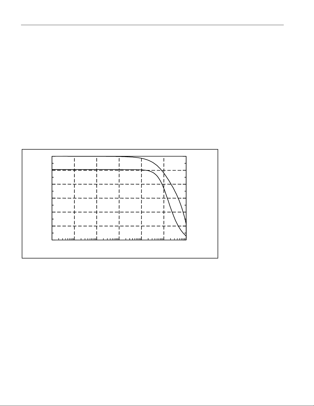
The open-loop amplifier response shown in Figure 6 was measured with I
the current-sense signal (across a sense resistor) and the 0.125V internal reference is produced so the voltage
across the sense resistor is maintained at V
in a closed-loop circuit.
IREF
= -1mA. An error signal between
CSOUT
Current-Sense Comparator (DS2712)
The comparator in the DS2712 switches between ON and OFF and is capable of driving a PNP bipolar or a PMOS
transistor, enabling the use of a switched-mode power stage. Hysteresis on the comparator input provides noise
rejection. In the closed-loop regulation circuit of Figure 5, the comparator regulates voltage across the sense
resistor to a DC average of:
V
= V
RSNS
- 0.5 x V
IREF
HYS-COMP
= 0.125V
10 of 14

DS2711/DS2712: Loose Cell NiMH Charger
Charge Timer
The charge timer monitors the duration of charge in fast and top-off charge phases, and is reset at the beginning of
each phase. The time-out period is set with an external resistor connected from the TMR pin to V
. Resistors can
SS
be selected to support fast-charge time-out periods of 0.5 to 10 hours and top-off charge time-out periods of 0.25 to
5 hours. If the timer expires in fast-charge, the timer count is reset and charging proceeds to the top-off charge
phase. The top-off time-out period is half of the fast charge time-out period. If the timer expires in top-off, charging
proceeds to the maintenance phase. The programmed charge time approximately follows the equation:
t = 1.5 x R / 1000 (time in minutes)
Suspend
Suspension of charge activity is possible by floating the TMR pin. The CC1 and CC2 outputs become high-Z and
the charge timer stops. The state machine and all timers are reset to their presence test conditions.
Temperature Sense
Connecting an external 10kW NTC thermistor between THM1 or THM2 (THMx) and VSS, and a 10kW bias resistor
between V
and THMx allows the DS2711 to sense temperature. To sense the temperature of the battery cells,
DD
locate the thermistor close to the body of the battery cell so THM1 monitors the temperature of cell-1 and THM2
monitors the temperature of cell-2. Alternatively, the thermistor can sense ambient temperature by locating it away
from the cells. THM1 and THM2 can be connected together to sense temperature using a single thermistor and
bias resistor. The temperature qualification function can be defeated by connecting THM1 and THM2 to a single
resistor-divider supplying a voltage between the Thermistor-Min and Thermistor-Max threshold voltages. Several
recommended 10kW thermistors are shown in Table 2.
Min, Max Temperature Compare
The voltage thresholds of the THMx inputs (VTHM-MIN, VTHM-MAX) are set to allow fast charging to start if 0°C <
T
< 45°C when using the recommended 10kW bias and 10kW thermistor. If fast charging is in progress, and the
A
voltage on THMx reaches VTHM-STOP, fast charging stops and the maintenance phase begins.
Table 2. THM1, THM2 THRESHOLDS
THM
THRESHOLD
RATIO
OF V
DD
THERMISTOR
RESISTANCE
(W)
Semitec
103AT-2
MIN 0.73 27.04k
MAX 0.33 4.925k
STOP 0.29 4.085k
45°C 42°C
50°C 47°C
Figure 7. CELL VOLTAGE SENSE POINTS
Series Configuration
Charge Source
CC1
VP2
Vcell2
VP1
Vcell1
VN1
VN0
Charge Source
TEMPERATURE (°C)
Fenwal
197-103LAG-A01
173-103LAF-301
0°C 4°C
Parallel Configuration
CC2
CC1
VP1
Vcell1 Vcell2
VN1
VN0
VP2
11 of 14

DS2711/DS2712: Loose Cell NiMH Charger
Cell Voltage Monitoring
In the 2-cell series mode, the voltage difference between VP2 and VP1 is used to determine the Vcell2 voltage in
the two-cell series stack. The voltage difference between VP1 and VN1 is used to determine the Vcell1 voltage. In
the 1-cell series mode, the difference between VP1 and VN1 is used as the cell voltage. VP2 can be left floating in
the 1-cell series mode. In parallel mode, the difference between VP2 and VN1 is used for the Vcell2 voltage, and
the difference between VP1 and VN1 is used for Vcell1 voltage.
Individual cell voltages are monitored for minimum and maximum values, using the V
threshold limits. Upon inserting a cell or power-up with cells inserted, cell voltages must be less than the V
threshold before charging begins. The V
threshold determines whether a precharge cycle should precede the
BAT-MIN
BAT-MIN
, V
BAT-MAX1
and V
BAT-MAX2
BAT-MAX1
fast charge cycle, and when to transition from precharge to fast charge. Once fast charging commences, cell
voltages are compared to the V
BAT-MAX2
threshold once per second. The comparison occurs while the charge
control pin (CC1 or CC2) controlling current to the cell is active (low). When the charge control pin is active so
charge is applied to the cell, the cell voltage is referred to as the V
inactive, the cell voltage is referred to as the V
voltage. If V
OFF
BAT-MAX2
voltage. When the charge-control pin is
ON
is exceeded in fast charge, charging is halted
and a fault condition is displayed. While fast charge is in progress, cell voltage measurements are stored and
compared to future measurements for charge termination and cell test purposes.
Two types of tests are performed to detect primary alkaline and lithium cells or defective NiMH or NiCd secondary
cells. Cells are tested individually in the series and parallel configurations, so that a single improper or defective
cell can be detected quickly. In the series configuration, a single defective cell will terminate charge for both cells,
whereas the parallel mode continues charging the good cell and stops charging the defective cell.
V
is set by the resistance from the CTST pin to ground. The nominal sensitivity of 100mV is set by connecting
CTST
an 80kW resistor between CTST and V
. The detection threshold can be set from 32mV to 400mV. The following
SS
formula approximates the setting for the detection threshold.
V
= 8000/R (value in volts)
CTST
-∆V and Flat Voltage Termination
During fast charge, -DV detection is performed by comparing successive voltage measurements for a drop of 2mV
in the cell voltage. A hold-off period for -DV detection begins at the start of fast charging and prevents false
termination in the first few minutes of the charge cycle. Once the hold-off period expires, cell voltage
measurements are acquired every 32 clock cycles (during the CCx off time). When a newly acquired voltage
measurement is greater than any previous one, the new value is retained as the maximum value. When the cell
voltage no longer increases, the maximum value is retained and compared against subsequent values. If the cell
voltage drops by the -DV threshold, V
that the maximum value persists for a period of 16 minutes (t
, (2mV typ), fast charging is terminated. If the cell voltage remains flat such
-DV
), fast charge terminates and top-off charging
FLAT
begins.
Top-Off and Maintenance
In top-off mode, the charger scales the cell current to 25% of the fast charge current. The charge timer is reset and
restarted with a time-out period of one half the fast-charge duration. When the charge timer expires in top-off, the
charger enters maintenance and delivers 1/64 of the charge source current to the cells. Maintenance charge
continuous until power is removed, the cell(s) are removed or the DS2711/DS2712 is cycled into and out of
suspend mode by floating the TMR pin.
Selecting the Charge Mode
The charge mode configuration is selected by testing the LED2 pin during startup. An internal current source tests
the state of the LED2 pin by pulling up and pulling down on the pin to determine if it is high, low, or floating. The
recommended pullup or pulldown resistor value (if used) is 100kW. In the parallel charging circuit diagrams on page
8, no resistor is shown. The current path through the LED and 270W resistor is sufficient to pull the LED2 pin high
at power-up to select the parallel mode. Refer to the mode test current (I
Characteristics table to select other pullup values.
) specification in the Electrical
MTST
12 of 14

DS2711/DS2712: Loose Cell NiMH Charger
Table 3. CHARGE MODE SELECTION
LED2 PIN STRAPPING MODE
Low 1-Cell Series
Floating 2-Cell Series
High Parallel
CC1 and CC2 Outputs
The CC1 and CC2 operate as open-drain outputs that drive active low to connect the charge source to the battery
cell. During charge, the behavior of the CC1 and CC2 outputs depends on the charge-mode configuration. In
parallel mode, CC1 and CC2 are driven low in alternating time slots. The charge source is loaded by just one cell
during any time slot. In the 1-cell and 2-cell series mode, only CC1 is driven. Except for the periodic performance of
impedance and -DV tests, series mode charging is continuous during the fast charge phase rather than pulsed in
parallel mode.
Parallel Mode Fast Charge
Referring to Figure 4. PARALLEL CONFIGURATION WITH EXTERNAL CURRENT REGULATION, CC1 controls
the PNP switch that gates current to the cell in slot 1. CC2 controls the PNP switch that gates current to the cell in
slot 2. During fast charge, current is gated to each slot sequentially, with charge pulses occurring in alternating time
frames. The cell in one slot charges while the other relaxes and the effective fast-charge current is 48.4% of the
magnitude set by the charge-source current limit. The parallel configuration skips a charge pulse every 32 clock
cycles to facilitate independent testing of the open- and closed-circuit cell voltages (V
Since the charge regime of each cell is independent, one cell may complete a charge phase before the other. The
more fully charged cell of a pair inserted at the same time could terminate fast charge by -DV, then charge in top-off
while the less charged cell continues in fast charge. In the case of an improper or faulty cell (e.g., alkaline) being
inserted along with a proper cell (NiMH or NiCd), charging of the faulty cell would be stopped, while the proper cell
is charged to full.
and VON, respectively).
OFF
Series Mode Fast Charge
Referring to Figure 3. SERIES CONFIGURATION WITH EXTERNAL CURRENT REGULATION, CC1 controls the
PNP switch that gates current to the cell(s). In series mode, 1 or 2 cells can be charged, depending on whether the
1-cell or 2-cell series mode has been selected. During fast charge, current is gated to the cell(s) almost
continuously, with the effective fast-charge current approximately equal to current limit of the charge source. The
series configuration deactivates CC1 briefly every 32 clock cycles to facilitate independent testing of V
of each cell. The one second deactivation makes the duty factor 0.969 and therefore the effective current equals
approximately 97% of the charge-source current limit. In the 2-cell series mode, the characteristics of each cell are
evaluated individually; however charging stops if either cell is determined to be improper or faulty.
In the 1-cell charge series mode, CC1 gates the charge current as in the 2-cell series mode. The cell voltage is
monitored between VP1 and VN1, and temperature is monitored with THM1. The VP2 and THM2 pins can be left
floating in the 1-cell series mode.
and VON
OFF
EXAMPLE CAPACITIES AND CHARGE RATES
Parallel Charging Example:
A 1700mAH cell is charged using a 1A regulated charge source. During fast charge, the cell is charged at a duty
factor of 0.484 and receives an effective charge current of 0.484A. In terms of C-rate, this is 484mA/1700mAh =
0.285°C (or C/3.5). During precharge and top-off, the duty factor is 0.125 (i.e., 1/8), for an effective average
current of 125mA, corresponding to a C-rate of 125/1700 = 0.073C (or C/13.6). Similarly, in maintenance mode, the
duty factor is 0.0156 (i.e., 1/64) and the C-rate is 15.6/1700 = 0.0092 ( or C/109). The C-rates for charging 3
different cell capacities using a 500mA and a 1000mA current source are shown in Table 4.
13 of 14

DS2711/DS2712: Loose Cell NiMH Charger
Table 4. PARALLEL CONFIGURATION, EACH CELL
MODE CURRENT LIMIT 500mA CURRENT LIMIT 1000mA
Cell Capacity 900mAH 1700mAH 2200mAH 900mAH 1700mAH 2200mAH
Fast C/3.72 C/7.02 C/9.08 C/1.86 C/3.51 C/4.54
Precharge/Top-Off C/14.4 C/27.2 C/35.2 C/7.20 C/13.6 C/17.6
Maintenance C/115 C/218 C/282 C/57.6 C/109 C/141
Series and Single Cell Charging Example:
In the series and single-cell modes, the effective fast charge current is equal to 0.969 times the regulated current
limit and the top-off current is 0.25 times the regulated current. The maintenance mode is identical to the parallel
charging rate, that is, 1/64 times the regulated current. The C-rates for charging 3 different cell capacities using a
500mA and a 1000mA current source are shown in the following table.
Table 5. SERIES CONFIGURATION, EACH CELL
MODE CURRENT LIMIT 500mA CURRENT LIMIT 1000mA
Cell Capacity 900mAH 1700mAH 2200mAH 900mAH 1700mAH 2200mAH
Fast C/1.86 C/3.51 C/4.54 C/0.93 C/1.75 C/2.27
Precharge/Top-Off C/7.20 C/13.6 C/17.6 C/3.60 C/6.80 C/8.80
Maintenance C/115 C/218 C/282 C/57.6 C/109 C/141
LED1 and LED2 Outputs, MODE-Select Input
Open-drain outputs LED1 and LED2 pull low to indicate charge status. When inactive, the outputs are high
impedance. LED1 displays the status for the cell monitored by VP1 and LED2 displays the status for the cell
monitored by VP2.
The LED pins drive low in three “blink” patterns to annunciate the charge status. Table 6 summarizes the LED
operation in each display mode (DM0, DM1, DM2) for each charge condition. In parallel mode, LED1 indicates the
status of the cell whose positive terminal is connected to VP1 and LED2 indicates the status of the cell whose
positive terminal is connected to VP2. In series mode, LED1 indicates the charge status for both cells since they
are charged in series.
Table 6. DISPLAY PATTERNS BY DISPLAY MODE AND CHARGE ACTIVITY
DISPLAY MODE CHARGE ACTIVITY
PRE/FAST/TOP-
OFF
CHARGING
0.80s Low
0.16s High-Z
MAINTENANCE FAULT
0.80s Low
0.16s High-Z
Low
DMSEL PIN
DM0
DM1
DM2
High-Z = High Impedance
NO
BATTERY
Low High-Z Low
Float High-Z Low High-Z
High High-Z
Package Information
For the latest package outline information, go to www.maxim-ic.com/DallasPackInfo.
14 of 14
0.48s Low
0.48s High-Z
0.16s Low
0.16s High-Z
0.16s Low
0.16s High-Z
 Loading...