

Page 1

r
www.maxim-ic.com
GENERAL DESCRIPTION
The DS26401 is an octal, software-selectable T1, E1
or J1 framer. It is composed of eight fram er/formatters
and a system (backplane) interface. Each framer has
an HDLC controller that can be mapped to any DS0
or FDL (T1)/Sa (E1) bit. The DS26401 also includes a
full-feature BERT device, which can be used with any
of the eight T1/E1 ports, and an internal clock adapter
useful for creating synchronous, high frequency
backplane timing. The DS26401 is controlled through
an 8-bit parallel port that can be configured for
nonmultiplexed Intel or Motorola operation.
APPLICATIONS
Line Cards Routers
Add-Drop Multiplexers IMA
DSLAMs ATM
Timing Systems WAN Interface
PBXs
Switches
Central Office Equipment
Go to www.maxim-ic.com/telecom for a complete list of
Telecommunications data sheets, evaluation kits, application
notes, and software downloads.
Customer-Premise
Equipment
DS26401
Octal T1/E1/J1 Frame
FEATURES
§ 8 Independent, Full-Featured T1/E1/J1
Framers/Formatters
§ Independent Transmit and Receive Paths
§ Flexible Signaling Extraction and Insertion
§ Alarm Detection and Insertion
§ Transmit Synchronizer
§ AMI, B8ZS, HDB3, NRZ Line Coding
§ Performance Monitor Counters
§ BOC Message Controller (T1)
§ Two-Frame Elastic Store Buffers for Each
Transmitter and Receiver
§ One HDLC Controller per Framer
§ RAI-CI and AIS-CI Support
§ Full-Feature BERT can be Mapped to Any Port
§ Flexible TDM Backplane Supports Bus Rates
from 1.544MHz to 16.384MHz
§ Internal Clock Generator (CLAD) Supplies
16.384MHz, 8.192MHz, 4.096MHz, or 2.048MHz
§ JTAG Test Port
§ Single 3.3V Supply with 5V Tolerant Inputs
§ 17mm x 17mm, 256-Pin BGA (1.00mm Pitch)
ORDERING INFORMATION
PART TEMP RANGE PIN-PACKAGE
DS26401
DS26401N -40°C to +85°C 256 BGA
0°C to +70°C 256 BGA
Note: Some revisions of this device may incorporate deviations from published specifications known as errata. Multiple revisions of any device
may be simultaneously available through various sales channels. For information about device errata, click here: www.maxim-ic.com/errata
1
REV: 072403
.
Page 2

DS26401 Octal T1/E1/J1 Framer
TABLE OF CONTENTS
1. APPLICABLE STANDARDS ........................................................................................................7
2. FEATURES ..................................................................................................................................8
2.1 FRAMER/FORMATTER .....................................................................................................................................8
2.2 SYSTEM INTERFACE........................................................................................................................................8
2.3 HDLC CONTROLLERS ....................................................................................................................................9
2.4 TEST AND DIAGNOSTICS .................................................................................................................................9
2.5 CONTROL PORT..............................................................................................................................................9
3. BLOCK DIAGRAMS...................................................................................................................10
4. SIGNAL LIST (SORTED BY SIGNAL NAME)............................................................................13
5. SIGNAL DESCRIPTIONS...........................................................................................................17
5.1 RECEIVE FRAMER SIGNALS...........................................................................................................................17
5.2 TRANSMIT FRAMER SIGNALS.........................................................................................................................19
5.3 PARALLEL CONTROL PORT............................................................................................................................20
5.4 SYSTEM INTERFACE......................................................................................................................................21
5.5 TEST............................................................................................................................................................22
6. REGISTER MAP.........................................................................................................................23
7. GLOBAL FUNCTIONS...............................................................................................................24
7.1 GLOBAL REGISTERS .....................................................................................................................................24
7.2 GLOBAL REGISTER DESCRIPTION AND OPERATION ........................................................................................25
7.3 IBO MULTIPLEXER........................................................................................................................................27
7.4 INTERRUPT TREE ..........................................................................................................................................37
8. T1 RECEIVER ............................................................................................................................38
8.1 T1 RECEIVER REGISTER MAP.......................................................................................................................38
8.2 T1 RECEIVE FRAMER DESCRIPTION AND OPERATION.....................................................................................43
8.3 RECEIVE MASTER-MODE REGISTER..............................................................................................................44
8.4 INTERRUPT INFORMATION REGISTER .............................................................................................................44
8.5 T1 RECEIVE CONTROL REGISTERS ...............................................................................................................45
8.6 H.100 (CT BUS) COMPATIBILITY...................................................................................................................50
8.7 T1 RECEIVE STATUS AND INFORMATION ........................................................................................................52
8.8 T1 RECEIVE-SIDE DIGITAL MILLIWATT CODE GENERATION ............................................................................63
8.9 T1 ERROR COUNT REGISTERS......................................................................................................................64
8.10 DS0 MONITORING FUNCTION ....................................................................................................................69
8.11 T1 RECEIVE SIGNALING OPERATION..........................................................................................................70
8.12 T1 RECEIVE PER-CHANNEL IDLE CODE INSERTION ....................................................................................76
8.13 RECEIVE-CHANNEL BLOCKING OPERATION ................................................................................................77
8.14 RECEIVE ELASTIC STORES OPERATION .....................................................................................................78
8.15 FRACTIONAL T1 SUPPORT (GAPPED-CLOCK MODE)...................................................................................82
8.16 T1 BIT-ORIENTED CODE (BOC) CONTROLLER...........................................................................................83
8.17 RECEIVE SLC-96 OPERATION...................................................................................................................85
8.18 RECEIVE FDL...........................................................................................................................................86
8.19 PROGRAMMABLE IN-BAND LOOP-CODE DETECTION ...................................................................................87
8.20 RECEIVE HDLC CONTROLLER...................................................................................................................92
8.21 INTERLEAVED PCM BUS OPERATION (IBO) .............................................................................................100
8.22 INTERFACING THE T1 RX FRAMER TO THE BERT .....................................................................................102
9. T1 TRANSMIT..........................................................................................................................104
9.1 T1 TRANSMIT REGISTER MAP .....................................................................................................................104
2
Page 3

DS26401 Octal T1/E1/J1 Framer
T1 TRANSMIT FORMATTER DESCRIPTION AND OPERATION...........................................................................108
9.2
9.3 TRANSMIT-MASTER MODE REGISTER ..........................................................................................................109
9.4 INTERRUPT INFORMATION REGISTERS .........................................................................................................109
9.5 T1 TRANSMIT CONTROL REGISTERS ...........................................................................................................110
9.6 T1 TRANSMIT STATUS AND INFORMATION ....................................................................................................115
9.7 T1 PER-CHANNEL LOOPBACK .....................................................................................................................118
9.8 T1 TRANSMIT DS0 MONITORING FUNCTION ................................................................................................119
9.9 T1 TRANSMIT SIGNALING OPERATION .........................................................................................................120
9.10 T1 TRANSMIT PER-CHANNEL IDLE CODE INSERTION ................................................................................123
9.11 T1 TRANSMIT CHANNEL BLOCKING REGISTERS........................................................................................124
9.12 T1 TRANSMIT ELASTIC STORES OPERATION ............................................................................................125
ELASTIC STORE DELAY AFTER INITIALIZATION ........................................................................................................126
9.13 FRACTIONAL T1 SUPPORT (GAPPED CLOCK MODE) .................................................................................129
9.14 T1 TRANSMIT BIT ORIENTED CODE (BOC) CONTROLLER .........................................................................130
9.15 T1 TRANSMIT FDL..................................................................................................................................131
9.16 TRANSMIT SLC–96 OPERATION ..............................................................................................................132
9.17 TRANSMIT HDLC CONTROLLER...............................................................................................................133
9.18 HDLC TRANSMIT EXAMPLE .....................................................................................................................141
9.19 PROGRAMMABLE IN-BAND LOOP-CODE GENERATOR................................................................................142
9.20 INTERLEAVED PCM BUS OPERATION (IBO) .............................................................................................144
9.21 INTERFACING THE T1 TX FORMATTER TO THE BERT ................................................................................146
9.22 T1 TRANSMIT SYNCHRONIZER .................................................................................................................148
10. E1 RECEIVER..........................................................................................................................150
10.1 E1 RECEIVER REGISTER MAP .................................................................................................................150
10.2 E1 RECEIVE FRAMER DESCRIPTION AND OPERATION...............................................................................155
10.3 RECEIVE MASTER MODE REGISTER.........................................................................................................156
10.4 INTERRUPT INFORMATION REGISTERS......................................................................................................157
10.5 E1 RECEIVE CONTROL REGISTERS .........................................................................................................158
10.6 H.100 (CT BUS) COMPATIBILITY.............................................................................................................162
10.7 E1 RECEIVE STATUS AND INFORMATION ..................................................................................................164
10.8 E1 ERROR COUNT REGISTERS................................................................................................................175
10.9 DS0 MONITORING FUNCTION ..................................................................................................................181
10.10 E1 RECEIVE SIGNALING OPERATION........................................................................................................182
10.11 E1 RECEIVE PER-CHANNEL IDLE CODE INSERTION ..................................................................................187
10.12 RECEIVE CHANNEL BLOCKING OPERATION...............................................................................................188
10.13 RECEIVE ELASTIC STORES OPERATION ...................................................................................................189
ELASTIC STORE DELAY AFTER INITIALIZATION ........................................................................................................192
10.14 FRACTIONAL E1 SUPPORT (GAPPED CLOCK MODE).................................................................................193
10.15 ADDITIONAL SA-BIT AND SI-BIT RECEIVE OPERATION (E1 MODE).............................................................194
10.16 RECEIVE HDLC CONTROLLER.................................................................................................................200
HDLC RECEIVE EXAMPLE .....................................................................................................................................207
10.17 INTERLEAVED PCM BUS OPERATION (IBO) .............................................................................................208
10.18 INTERFACING THE E1 RX FRAMER TO THE BERT .....................................................................................210
11. E1 TRANSMIT..........................................................................................................................212
11.1 E1 TRANSMIT REGISTER MAP .................................................................................................................212
11.2 E1 TRANSMIT FORMATTER DESCRIPTION AND OPERATION .......................................................................216
11.3 TRANSMIT MASTER MODE REGISTER.......................................................................................................217
11.4 INTERRUPT INFORMATION REGISTERS......................................................................................................218
11.5 E1 TRANSMIT CONTROL REGISTERS .......................................................................................................219
11.6 AUTOMATIC ALARM GENERATION ............................................................................................................221
11.7 G.706 INTERMEDIATE CRC-4 UPDATING (E1 MODE ONLY)......................................................................223
11.8 E1 TRANSMIT STATUS AND INFORMATION ................................................................................................225
11.9 PER-CHANNEL LOOPBACK.......................................................................................................................228
11.10 E1 TRANSMIT DS0 MONITORING FUNCTION.............................................................................................229
11.11 E1 TRANSMIT SIGNALING OPERATION......................................................................................................230
11.12 E1 TRANSMIT PER-CHANNEL IDLE CODE INSERTION ................................................................................233
3
Page 4

DS26401 Octal T1/E1/J1 Framer
E1 TRANSMIT CHANNEL BLOCKING REGISTERS .......................................................................................234
11.13
11.14 E1 TRANSMIT ELASTIC STORES OPERATION ............................................................................................235
ELASTIC STORE DELAY AFTER INITIALIZATION ........................................................................................................236
11.15 FRACTIONAL E1 SUPPORT (GAPPED CLOCK MODE).................................................................................239
11.16 ADDITIONAL (SA) AND INTERNATIONAL (SI) BIT OPERATION (E1 MODE) ....................................................240
11.17 TRANSMIT HDLC CONTROLLER...............................................................................................................247
11.18 HDLC TRANSMIT EXAMPLE .....................................................................................................................255
11.19 INTERLEAVED PCM BUS OPERATION (IBO) .............................................................................................256
11.20 INTERFACING THE E1 TRANSMITTER TO THE BERT ..................................................................................258
11.21 E1 TRANSMIT SYNCHRONIZER .................................................................................................................260
12. BERT........................................................................................................................................262
12.1 BERT REGISTERS ..................................................................................................................................262
12.2 BERT DESCRIPTION AND OPERATION .....................................................................................................263
12.3 PATTERN GENERATION ...........................................................................................................................264
12.4 PATTERN SYNCHRONIZATION...................................................................................................................265
12.5 BER CALCULATION.................................................................................................................................265
12.6 ERROR GENERATION ..............................................................................................................................265
12.7 BERT CONTROL REGISTERS ..................................................................................................................267
12.8 BERT STATUS REGISTER .......................................................................................................................271
12.9 PSEUDORANDOM PATTERN REGISTERS ...................................................................................................272
12.10 COUNT REGISTERS .................................................................................................................................274
12.11 RAM ACCESS.........................................................................................................................................275
13. FUNCTIONAL TIMING ............................................................................................................. 276
13.1 DELAYS ..................................................................................................................................................276
13.2 T1 RECEIVER FUNCTIONAL TIMING DIAGRAMS .........................................................................................277
13.3 T1 TRANSMITTER FUNCTIONAL TIMING DIAGRAMS ...................................................................................282
13.4 E1 RECEIVER FUNCTIONAL TIMING DIAGRAMS.........................................................................................286
13.5 E1 TRANSMITTER FUNCTIONAL TIMING DIAGRAMS ...................................................................................288
14. OPERATING PARAMETERS...................................................................................................291
15. TIMING.....................................................................................................................................292
15.1 MICROPROCESSOR BUS AC CHARACTERISTICS .......................................................................................292
15.2 RECEIVER AC CHARACTERISTICS............................................................................................................295
15.3 TRANSMIT AC CHARACTERISTICS ............................................................................................................298
15.4 JTAG INTERFACE TIMING .......................................................................................................................301
15.5 SYSTEM CLOCK AC CHARACTERISTICS ...................................................................................................301
16. JTAG BOUNDARY SCAN ARCHITECTURE AND TEST ACCESS PORT...............................302
16.1 TAP CONTROLLER STATE MACHINE ........................................................................................................303
16.2 INSTRUCTION REGISTER..........................................................................................................................306
16.3 TEST REGISTERS....................................................................................................................................307
17. PACKAGE INFORMATION ...................................................................................................... 308
18. THERMAL INFORMATION ...................................................................................................... 309
19. REVISION HISTORY................................................................................................................309
4
Page 5

DS26401 Octal T1/E1/J1 Framer
LIST OF FIGURES
Figure 3-1. Block Diagram ........................................................................................................................................10
Figure 3-2. Typical PLL Connection..........................................................................................................................11
Figure 3-3. Typical Bipolar Network-Side Interface to Framers ................................................................................11
Figure 3-4. Typical NRZ Network-Side Interface to Framers....................................................................................12
Figure 7-1. Internal IBO Multiplexer Equivalent Circuit—4.096MHz .........................................................................28
Figure 7-2. Internal IBO Multiplexer Equivalent Circuit—8.192MHz .........................................................................29
Figure 7-3. Internal IBO Multiplexer Equivalent Circuit—16.394MHz ......................................................................30
Figure 8-1. RSYNC Input in H.100 (CT Bus) Mode ..................................................................................................50
Figure 8-2. TSSYNC Input in H.100 (CT Bus) Mode ................................................................................................51
Figure 8-3. Receive HDLC Example........................................................................................................................99
Figure 9-1. HDLC Message Transmit Example .....................................................................................................141
Figure 10-1. RSYNC Input in H.100 (CT Bus) Mode ..............................................................................................162
Figure 10-2. TSSYNC Input in H.100 (CT Bus) Mode ............................................................................................163
Figure 10-3. Receive HDLC Example....................................................................................................................207
Figure 11-1. HDLC Message Transmit Example ....................................................................................................255
Figure 12-1. Shared BERT Block Diagram .............................................................................................................266
Figure 13-1. T1 Receive-Side D4 Timing ...............................................................................................................277
Figure 13-2. T1 Receive-Side ESF Timing .............................................................................................................277
Figure 13-3. T1 Receive-Side Boundary Timing (Elastic Store Disabled) .............................................................278
Figure 13-4. T1 Receive-Side 1.544MHz Boundary Timing (Elastic Store Enabled)..............................................278
Figure 13-5. T1 Receive-Side 2.048MHz Boundary Timing (Elastic Store Enabled)..............................................279
Figure 13-6. T1 Receive-Side Interleave Bus Operation, BYTE Mode...................................................................280
Figure 13-7. T1 Receive-Side Interleave Bus Operation, FRAME Mode................................................................281
Figure 13-8. T1 Transmit-Side D4 Timing ..............................................................................................................282
Figure 13-9. T1 Transmit-Side ESF Timing ............................................................................................................282
Figure 13-10. T1 Transmit-Side Boundary Timing (Elastic Store Disabled) ...........................................................283
Figure 13-11. T1 Transmit-Side 1.544MHz Boundary Timing (Elastic Store Enabled) ..........................................283
Figure 13-12. T1 Transmit-Side 2.048MHz Boundary Timing (Elastic Store Enabled) ..........................................284
Figure 13-13. T1 Transmit-Side Interleave Bus Operation, BYTE Mode................................................................284
Figure 13-14. T1 Transmit Interleave Bus Operation, FRAME Mode.....................................................................285
Figure 13-15. E1 Receive-Side Timing ...................................................................................................................286
Figure 13-16. E1 Receive-Side Boundary Timing (Elastic Store Disabled) ............................................................286
Figure 13-17. E1 Receive-Side 1.544MHz Boundary Timing (Elastic Store Enabled) ...........................................287
Figure 13-18. E1 Receive-Side 2.048MHz Boundary Timing (Elastic Store Enabled) ...........................................287
Figure 13-19. E1 Transmit-Side Timing..................................................................................................................288
Figure 13-20. E1 Transmit-Side Boundary Timing (Elastic Store Disabled) ...........................................................288
Figure 13-21. E1 Transmit-Side 1.544MHz Boundary Timing (Elastic Store Enabled) .........................................289
Figure 13-22. E1 Transmit-Side 2.048MHz Boundary Timing (Elastic Store Enabled) ..........................................289
Figure 13-23. E1 G.802 Timing...............................................................................................................................290
Figure 15-1. Intel Bus Read Timing (BTS = 0).......................................................................................................293
Figure 15-2. Intel Bus Write Timing (BTS = 0).......................................................................................................293
Figure 15-3. Motorola Bus Read Timing (BTS = 1) ...............................................................................................294
Figure 15-4. Motorola Bus Write Timing (BTS = 1) ...............................................................................................294
Figure 15-5. Receive Framer Timing—Backplane (T1 Mode) ...............................................................................295
Figure 15-6. Receive-Side Timing—Elastic Store Enabled (T1 Mode)..................................................................296
Figure 15-7. Receive Framer Timing—Line Side ..................................................................................................297
Figure 15-8. Transmit Formatter Timing—Backplane ...........................................................................................299
Figure 15-9. Transmit Formatter Timing, Elastic Store Enabled ...........................................................................300
Figure 15-10. Transmit Formatter Timing—Line Side ...........................................................................................300
Figure 15-11. JTAG Interface Timing Diagram.......................................................................................................301
Figure 16-1. JTAG Functional Block Diagram ........................................................................................................302
Figure 16-2. Tap Controller State Diagram............................................................................................................303
5
Page 6

DS26401 Octal T1/E1/J1 Framer
LIST OF TABLES
Table 7-1. Pin Functions with IBO Mux Enabled ......................................................................................................31
Table 8-1. T1 Alarm Criteria .....................................................................................................................................53
Table 8-2. T1 Line-Code Violation Counting Options ...............................................................................................66
Table 8-3. T1 Path-Code Violation Counting Arrangements ....................................................................................67
Table 8-4. T1 Frames Out-of-Sync Counting Arrangements ....................................................................................68
Table 10-1. E1 Sync/Resync Criteria......................................................................................................................159
Table 10-2. E1 Alarm Criteria .................................................................................................................................165
Table 10-3. E1 Line Code Violation Counting Options ...........................................................................................177
Table 12-1. Pseudo-Random Pattern Generation ..................................................................................................273
Table 13-1. Throughput Delays ..............................................................................................................................276
Table 16-1. Instruction Codes for IEEE 1149.1 Architecture ..................................................................................306
Table 16-2. ID Code Structure ................................................................................................................................307
6
Page 7

DS26401 Octal T1/E1/J1 Framer
1. APPLICABLE STANDARDS
The DS26401 conforms to the applicable parts of the following standards.
SPECIFICATION TITLE
ANSI
T1.102-1993 Digital Hierarchy—Electrical Interfaces
T1.107-1995 Digital Hierarchy—Formats Specification
T1.231-1997 Digital Hierarchy—Layer 1 In-Service Digital Transmission Performance Monitoring
T1.403-1999 Network and Customer Installation Interfaces—DS1 Electrical Interface
AT&T
TR54016
TR62411 High Capacity Digital Service Channel Interface Specification
ITU
G.704, 1995
G.706, 1991
G.732, 1993 Characteristics of Primary PCM Multiplex Equipment Operating at 2048 kbit/s
G.736, 1993 Characteristics of a synchronous digital multiplex equipment operating at 2048 kbit/s
G.775, 1994 Loss Of Signal (LOS) and Alarm Indication Signal (AIS) Defect Detection and Clearance Criteria
G.823, 1993
I.431, 1993 Primary Rate User-Network Interface—Layer 1 Specification
O.151, 1992 Error Performance Measuring Equipment Operating at the Primary Rate and Above
O.161, 1988 In-service code violation monitors for digital systems
ETSI
ETS 300 011, 1998
ETS 300 166, 1993
ETS 300 233, 1994 Integrated Services Digital Network (ISDN); Access digital section for ISDN primary rate
CTR 4, 1995
I.432, 1993 B-ISDN User-Network Interface—Physical Layer Specification–ITU-T
CTR 12, 1993
CTR 13, 1996
TTC
JT-G.704, 1995 Frame Structures on Primary and Secondary Hierarchical Digital Interfaces
JTI.431, 1995 ISDN Primary Rate User-Network Interface Layer 1 Specification
Requirements for Interfacing Digital Terminal Equipment to Services Employing the Extended
Superframe Format
Synchronous Frame Structures used at 1544, 6312, 2048, 8488, and 44,736 kbit/s Hierarchical
Levels
Frame Alignment and Cyclic Redundancy Check (CRC) Procedures Relating to Basic Frame
Structures Defined in Recommendation G.704
The Control of Jitter and Wander Within Digital Networks Which are Based on the 2048kbps
Hierarchy
Integrated Services Digital Network (ISDN); Primary rate User-Network Interface (UNI); Part 1: Layer
1 specification
Transmission and multiplexing; Physical/electrical characteristics of hierarchical digital interfaces for
equipment using the 2048 kbit/s-based plesiochronous or synchronous digital hierarchies
Integrated Services Digital Network (ISDN); Attachment requirements for terminal equipment to
connect to an ISDN using ISDN primary rate access
Business Telecommunications (BT); Open Network Provision (ONP) technical requirements; 2048
kbit/s digital unstructured leased lines (D2048U) attachment requirements for terminal equipment
interface
Business Telecommunications (BTC); 2048 kbit/s digital structured leased lines (D2048S);
Attachment requirements for terminal equipment interface
7
Page 8

DS26401 Octal T1/E1/J1 Framer
2. FEATURES
2.1 Framer/Formatter
§ Fully Independent Transmit and Receive Functionality
§ Full Receive and Transmit Path Transparency
§ T1 Framing Formats D4 and ESF per T1.403, and Expanded SLC-96 Support (TR-TSY-008)
§ E1 FAS Framing and CRC-4 Multiframe per G.704/G.706 and G.732 CAS Multiframe
§ Detailed Alarm and Status Reporting with Optional Interrupt Support
§ Large Path and Line Error Counters for
T1: BPV, CV, CRC6, and Framing Bit Errors
E1: BPV, CV, CRC4, E-Bit, and Frame Alignment Errors
Timed or Manual Update Modes
§ DS1 Idle Code Generation on a Per-Channel Basis in Both Transmit and Receive Paths
User-Defined
Digital Milliwatt
§ ANSI T1.403-1998 Support
§ G.965 V5.2 Link Detect
§ Ability to Monitor One DS0 Channel in Both the Transmit and Receive Paths
§ In-Band Repeating Pattern Generators and Detectors
Three Independent Detectors
Patterns from 1 to 8 bits or 16 bits in Length
§ Bit Oriented Code (BOC) Support
§ Flexible Signaling Support
Software- or Hardware-Based
Interrupt Generated on Change of Signaling Data
Signaling Debounce
Optional Receive Signaling Freeze on Loss of Frame (LOF), Loss of Signal (LOS), or Change-of-Frame
Alignment
§ Hardware Pins Provided to Indicate Loss of Frame, Loss of Signal, Loss-of-Transmit Clock (LOTC), or
Signaling Freeze Condition
§ Automatic RAI Generation to ETS 300 011 Specifications
§ RAI-CI and AIS-CI Support
§ Expanded Access to Sa and Si Bits
§ Option to Extend Carrier Loss Criteria to a 1ms Period as per ETS 300 233
§ Japanese J1 Support
Ability to Calculate and Check CRC6 According to the Japanese Standard
Ability to Generate Yellow Alarm According to the Japanese Standard
2.2 System Interface
§ Independent Two-Frame Receive and Transmit Elastic Stores
Independent Control and Clocking
Controlled Slip Capability with Status
Minimum Delay Mode Supported
§ Maximum Backplane Rate of 16.384MHz in IBO Mode
§ Supports T1 to E1 Conversion
§ Programmable Output Clocks for Fractional T1, E1, H0, and H12 Applications
§ Interleaving PCM Bus Operation (IBO)
§ Hardware Signaling Capability
Receive Signaling Reinsertion to a Backplane Multiframe Sync
Availability of Signaling in a Separate PCM Data Stream
Signaling Freezing
§ Ability to Pass the T1 F-Bit Position Through the Elastic Stores in the 2.048MHz Backplane Mode
§ User-Selectable Synthesized Clock Output
8
Page 9

2.3 HDLC Controllers
§ HDLC Engine (One per Framer):
§ Independent 64-byte Rx and Tx Buffers with Interrupt Support
§ Access FDL, Sa, or Single DS0 Channel
§ Compatible with Polled or Interrupt Driven Environments
2.4 Test and Diagnostics
§ Global, Full-Feature BERT
Any Pseudo-Random Pattern Up to 2
Up to 32 Taps can be Used Simultaneously
User-Defined Repetitive Patterns Up to 512 Bytes in Length
Large, 48-Bit Error and Bit Counters
Map to Any Framer/DS0/FDL (T1) or Sa Bits (E1)
§ Programmable Error Insertion
§ BPV Insertion
§ F-Bit Corruption for Line Testing
§ Loopbacks
Remote
Local
Per-Channel
§ IEEE 1149.1 Support
32
- 1
DS26401 Octal T1/E1/J1 Framer
2.5 Control Port
§ 8-Bit Parallel Control Port
§ Intel or Motorola Nonmultiplexed Support
§ Flexible Status Registers Support Polled, Interrupt, or Hybrid Program Environments
§ Software Reset Supported
§ Hardware Reset Pin
9
Page 10
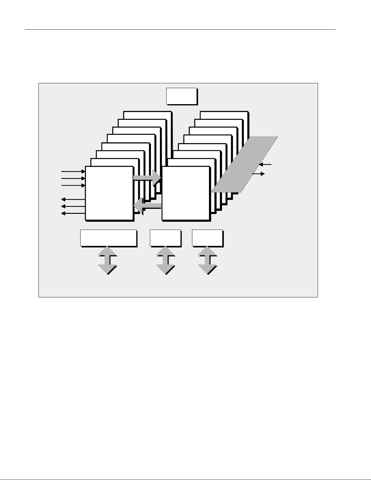
3. BLOCK DIAGRAMS
Figure 3-1. Block Diagram
DS26401 Octal T1/E1/J1 Framer
DS26401
RPOS
RNEG
RCLK
TPOS
TNEG
TCLKO
FRAMER #7
FRAMER #6
FRAMER #5
FRAMER #4
FRAMER
T1/E1
T1/E1
FRAMER #3
FRAMER
FRAMER
T1/E1
T1/E1
FRAMER #2
FRAMER
FRAMER
T1/E1
T1/E1
FRAMER
FRAMER
T1/E1
T1/E1
FRAMER
FRAMER
T1/E1
FRAMER
FRAMER
T1/E1
FRAMER
FRAMER
HDLCs
HDLCs
HDLCs
HDLCs
HDLCs
HDLCs
HDLCs
HDLCs
HDLCs
HDLCs
HDLCs
HDLCs
MICRO PROCESSOR
INTERFACE
FRAMER #8
T1/E1
T1/E1
T1/E1
HDLCs
BERT
BACKPLANE
BACKPLANE
BACKPLANE
INTERFACE
INTERFACE
BACKPLANE
INTERFACE
INTERFACE
ELASTIC
ELASTIC
STORES
STORES
JTAG
PORT
THE BERT FUNCTION MAY
BE ASSIGNED TO ANY PORT
BACKPLANE
BACKPLANE
BACKPLANE
INTERFACE
BACKPLANE
BACKPLANE
INTERFACE
INTERFACE
BACKPLANE
BACKPLANE
INTERFACE
INTERFACE
BACKPLANE
BACKPLANE
INTERFACE
INTERFACE
INTERFACE
INTERFACE
ELASTIC
ELASTIC
ELASTIC
ELASTIC
STORES
STORES
STORES
STORES
ELASTIC
ELASTIC
ELASTIC
STORES
ELASTIC
ELASTIC
STORES
STORES
ELASTIC
ELASTIC
STORES
STORES
STORES
STORES
PLL
IBO
THE IBO FUNCTION ALLOWS
ACCESS TO ALL 8 PORTS
INDIVIDUALLY OR AS 4 GROUPS
OF 2, 2 GROUPS OF 4, OR 1 GROUP
OF 8 PORTS.
RECEIVE AND
TRANSMIT
BACKPLANE
SIGNALS
10
CONTROLLER
PORT
TEST
PORT
CLOCKS
Page 11
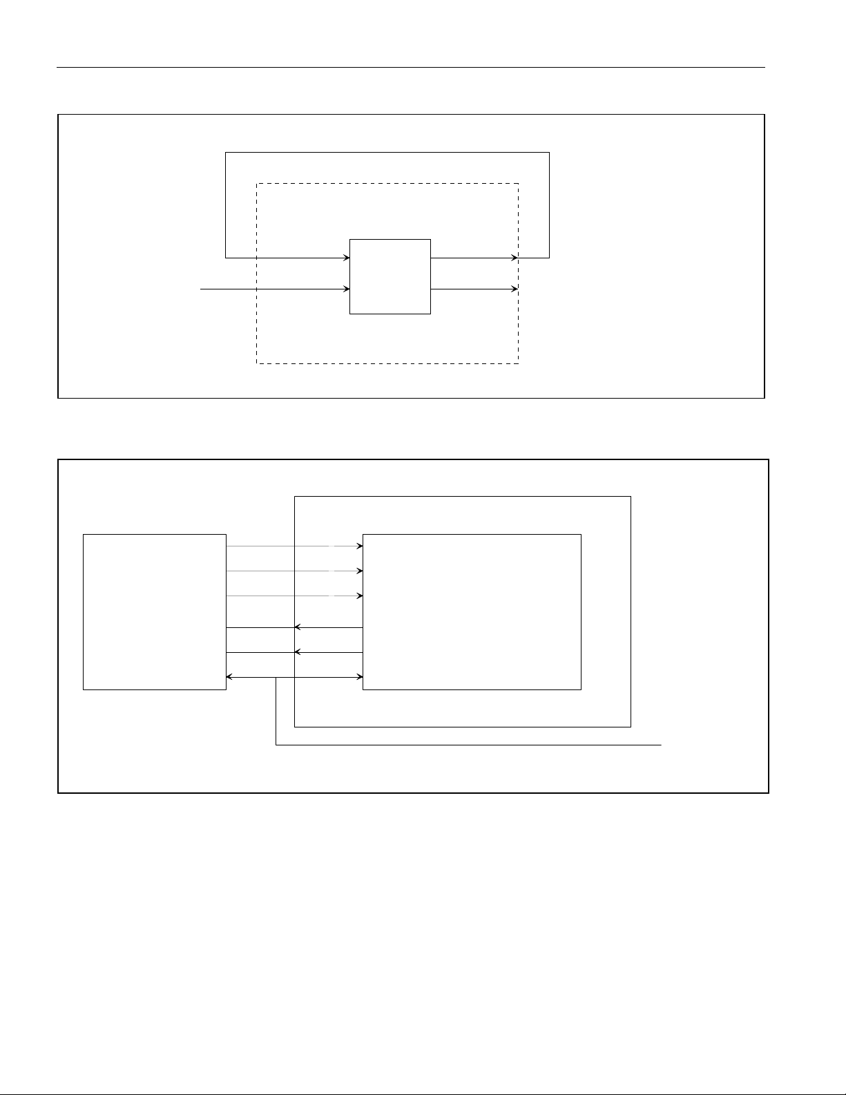
Figure 3-2. Typical PLL Connection
2.048MHz or
1.544MHz
GCLK_IN GCLK_OUT
REF_CLK
DS26401
PLL
BPCLK 2.048MHz, 4.096MHz
8.192MHz or 16.384MHz
Figure 3-3. Typical Bipolar Network-Side Interface to Framers
DS26401 Octal T1/E1/J1 Framer
DS26401
RPOSx
T1/E1 LIU
OR OTHER
SOURCE OF
BIPOLAR
DATA
RNEGx
RCLKx
TPOSx
TNEGx
TCLKx
1 OF 8 FRAMERS
2.048MHz or
1.544MHz
11
Page 12
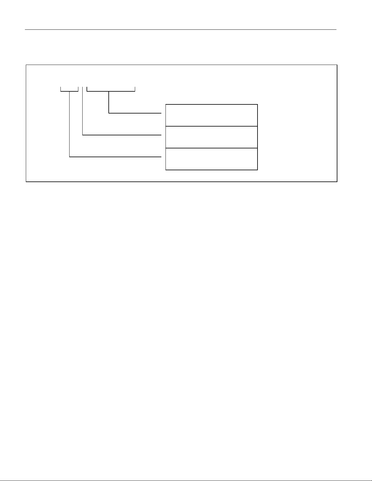
Figure 3-4. Typical NRZ Network-Side Interface to Framers
DS26401 Octal T1/E1/J1 Framer
RPOSx
RNEGx
DS26401
T1/E1 LIU
RCLKx
OR OTHER
SOURCE OF
NRZ DATA
NOTE: SET TCR3.7 = 1 TO SELECT NRZ MODE FOR TPOSx. SET RCR3.6 = 1 TO SELECT NRZ MODE FOR RPOSx.
TPOSx
TNEGx
TCLKx
1 OF 8 FRAMERS
2.048MHz or
1.544MHz
12
Page 13

4. SIGNAL LIST (SORTED BY SIGNAL NAME)
PIN NAME TYPE FUNCTION
B5
A5
C6
E8
A6
B6
D7
C7
A7
D8
C8
A8
F16 BPCLK O Programmable Backplane Clock
B2 BTS I Motorola or Intel Bus Type Select
B4
A1
C4
A2
B3
D5
A3
D6
A4
G16 GCLK_IN I Global Clock Input
G13 GCLK_OUT O Global Clock Output
R12 HIZE I High-Z Enable
E9
N10 JTCLK I JTAG Clock
T11 JTDI I JTAG Data Input
P11 JTDO O JTAG Data Output
T10 JTMS I JTAG Test Mode Select
R11 JTRST I JTAG Reset
B7, B13, D2, D15, E6,
E14, F2, G14, J16, M9,
N15, P2, P8, R5
B1 RCHBLK/CLK1 O Rx Channel Block/Clock for Framer 1
H1 RCHBLK/CLK2 O Rx Channel Block/Clock for Framer 2
L5 RCHBLK/CLK3 O Rx Channel Block/Clock for Framer 3
P6 RCHBLK/CLK4 O Rx Channel Block/Clock for Framer 4
N11 RCHBLK/CLK5 O Rx Channel Block/Clock for Framer 5
M15 RCHBLK/CLK6 O Rx Channel Block/Clock for Framer 6
E15 RCHBLK/CLK7 O Rx Channel Block/Clock for Framer 7
A13 RCHBLK/CLK8 O Rx Channel Block/Clock for Framer 8
C2 RCLK1 I Rx Clock for Framer 1
H4 RCLK2 I Rx Clock for Framer 2
L4 RCLK3 I Rx Clock for Framer 3
N6 RCLK4 I Rx Clock for Framer 4
M11 RCLK5 I Rx Clock for Framer 5
L14 RCLK6 I Rx Clock for Framer 6
E16 RCLK7 I Rx Clock for Framer 7
C12 RCLK8 I Rx Clock for Framer 8
E7
F15 REF_CLK I Reference Clock (1.544MHz/2.048MHz)
T12
E5 RF/RMSYNC1 O Rx Frame/MF Sync for Framer 1
H3 RF/RMSYNC2 O Rx Frame/MF Sync for Framer 2
N1 RF/RMSYNC3 O Rx Frame/MF Sync for Framer 3
T5 RF/RMSYNC4 O Rx Frame/MF Sync for Framer 4
T13 RF/RMSYNC5 O Rx Frame/MF Sync for Framer 5
13
ADDR0 I
ADDR1 I
ADDR2 I
ADDR3 I
ADDR4 I
ADDR5 I
ADDR6 I
ADDR7 I
ADDR8 I
ADDR9 I
ADDR10 I
ADDR11 I
CS
DATA0 I/O
DATA1 I/O
DATA2 I/O
DATA3 I/O
DATA4 I/O
DATA5 I/O
DATA6 I/O
DATA7 I/O
INT
N.C. No Connect
RD (DS)
RESET
mP Address Bus Bit 0
mP Address Bus Bit 1
mP Address Bus Bit 2
mP Address Bus Bit 3
mP Address Bus Bit 4
mP Address Bus Bit 5
mP Address Bus Bit 6
mP Address Bus Bit 7
mP Address Bus Bit 8
mP Address Bus Bit 9
mP Address Bus Bit 10
mP Address Bus Bit 11
I Chip Select (Active Low)
mP Data Bus Bit 0
mP Data Bus Bit 1
mP Data Bus Bit 2
mP Data Bus Bit 3
mP Data Bus Bit 4
mP Data Bus Bit 5
mP Data Bus Bit 6
mP Data Bus Bit 7
O Interrupt (Active Low)
I Read Strobe (Active Low)
I Global Reset (Active Low)
DS26401 Octal T1/E1/J1 Framer
Page 14

14
DS26401 Octal T1/E1/J1 Framer
PIN NAME TYPE FUNCTION
M16 RF/RMSYNC6 O Rx Frame/MF Sync for Framer 6
F14 RF/RMSYNC7 O Rx Frame/MF Sync for Framer 7
C13 RF/RMSYNC8 O Rx Frame/MF Sync for Framer 8
D1 RLOF/LOTC1 O RLOF or LOTC for Framer 1
K2 RLOF/LOTC2 O RLOF or LOTC for Framer 2
T1 RLOF/LOTC3 O RLOF or LOTC for Framer 3
P7 RLOF/LOTC4 O RLOF or LOTC for Framer 4
P13 RLOF/LOTC5 O RLOF or LOTC for Framer 5
K14 RLOF/LOTC6 O RLOF or LOTC for Framer 6
C15 RLOF/LOTC7 O RLOF or LOTC for Framer 7
D11 RLOF/LOTC8 O RLOF or LOTC for Framer 8
F5 RLOS/RSIGF1 O RLOS for Framer 1
J4 RLOS/RSIGF2 O RLOS for Framer 2
R2 RLOS/RSIGF3 O RLOS for Framer 3
T7 RLOS/RSIGF4 O RLOS for Framer 4
T16 RLOS/RSIGF5 O RLOS for Framer 5
K13 RLOS/RSIGF6 O RLOS for Framer 6
C16 RLOS/RSIGF7 O RLOS for Framer 7
A11 RLOS/RSIGF8 O RLOS for Framer 8
C1 RNEG1 I Rx Negative Data for Framer 1
H5 RNEG2 I Rx Negative Data for Framer 2
M4 RNEG3 I Rx Negative Data for Framer 3
R6 RNEG4 I Rx Negative Data for Framer 4
N12 RNEG5 I Rx Negative Data for Framer 5
L16 RNEG6 I Rx Negative Data for Framer 6
D16 RNEG7 I Rx Negative Data for Framer 7
B12 RNEG8 I Rx Negative Data for Framer 8
D4 RPOS1 I Rx Positive Data for Framer 1
J2 RPOS2 I Rx Positive Data for Framer 2
P1 RPOS3 I Rx Positive Data for Framer 3
T6 RPOS4 I Rx Positive Data for Framer 4
T14 RPOS5 I Rx Positive Data for Framer 5
L13 RPOS6 I Rx Positive Data for Framer 6
G12 RPOS7 I Rx Positive Data for Framer 7
E11 RPOS8 I Rx Positive Data for Framer 8
E4 RSER1 O Receive Serial Data for Framer 1
J1 RSER2 O Receive Serial Data for Framer 2
R1 RSER3 O Receive Serial Data for Framer 3
M7 RSER4 O Receive Serial Data for Framer 4
R14 RSER5 O Receive Serial Data for Framer 5
L15 RSER6 O Receive Serial Data for Framer 6
F12 RSER7 O Receive Serial Data for Framer 7
A12 RSER8 O Receive Serial Data for Framer 8
D3 RSIG1 O Receive Signaling Data for Framer 1
J3 RSIG2 O Receive Signaling Data for Framer 2
N3 RSIG3 O Receive Signaling Data for Framer 3
N7 RSIG4 O Receive Signaling Data for Framer 4
T15 RSIG5 O Receive Signaling Data for Framer 5
K12 RSIG6 O Receive Signaling Data for Framer 6
F13 RSIG7 O Receive Signaling Data for Framer 7
C11 RSIG8 O Receive Signaling Data for Framer 8
E3 RSYNC1 I/O Rx Frame/MF Sync for Framer 1
K1 RSYNC2 I/O Rx Frame/MF Sync for Framer 2
M5 RSYNC3 I/O Rx Frame/MF Sync for Framer 3
R7 RSYNC4 I/O Rx Frame/MF Sync for Framer 4
R15 RSYNC5 I/O Rx Frame/MF Sync for Framer 5
K16 RSYNC6 I/O Rx Frame/MF Sync for Framer 6
E13 RSYNC7 I/O Rx Frame/MF Sync for Framer 7
B11 RSYNC8 I/O Rx Frame/MF Sync for Framer 8
C3 RSYSCLK1 I Receive System Clock for Framer 1
H2 RSYSCLK2 I Receive System Clock for Framer 2
N2 RSYSCLK3 I Receive System Clock for Framer 3
M6 RSYSCLK4 I Receive System Clock for Framer 4
R13 RSYSCLK5 I Receive System Clock for Framer 5
Page 15

15
DS26401 Octal T1/E1/J1 Framer
PIN NAME TYPE FUNCTION
L12 RSYSCLK6 I Receive System Clock for Framer 6
H12 RSYSCLK7 I Receive System Clock for Framer 7
D12 RSYSCLK8 I Receive System Clock for Framer 8
F3 TCHBLK/CLK1 O Tx Channel Block/Clock for Framer 1
L2 TCHBLK/CLK2 O Tx Channel Block/Clock for Framer 2
R3 TCHBLK/CLK3 O Tx Channel Block/Clock for Framer 3
N8 TCHBLK/CLK4 O Tx Channel Block/Clock for Framer 4
P14 TCHBLK/CLK5 O Tx Channel Block/Clock for Framer 5
J15 TCHBLK/CLK6 O Tx Channel Block/Clock for Framer 6
A16 TCHBLK/CLK7 O Tx Channel Block/Clock for Framer 7
C10 TCHBLK/CLK8 O Tx Channel Block/Clock for Framer 8
F4 TCLK1 I Tx Clock for Framer 1
L1 TCLK2 I Tx Clock for Framer 2
T3 TCLK3 I Tx Clock for Framer 3
R9 TCLK4 I Tx Clock for Framer 4
P15 TCLK5 I Tx Clock for Framer 5
J13 TCLK6 I Tx Clock for Framer 6
B15 TCLK7 I Tx Clock for Framer 7
B10 TCLK8 I Tx Clock for Framer 8
G1 TCLKO1 O Tx Clock Output for Framer 1
M3 TCLKO2 O Tx Clock Output for Framer 2
P5 TCLKO3 O Tx Clock Output for Framer 3
P10 TCLKO4 O Tx Clock Output for Framer 4
M14 TCLKO5 O Tx Clock Output for Framer 5
H13 TCLKO6 O Tx Clock Output for Framer 6
D13 TCLKO7 O Tx Clock Output for Framer 7
B8 TCLKO8 O Tx Clock Output for Framer 8
P12 TESTPIN1 I Used for factory tests (Note 1)
M10 TESTPIN2 I Used for factory tests (Note 1)
G5 TNEG1 O Tx Negative Data for Framer 1
L3 TNEG2 O Tx Negative Data for Framer 2
P4 TNEG3 O Tx Negative Data for Framer 3
T9 TNEG4 O Tx Negative Data for Framer 4
P16 TNEG5 O Tx Negative Data for Framer 5
H15 TNEG6 O Tx Negative Data for Framer 6
A15 TNEG7 O Tx Negative Data for Framer 7
B9 TNEG8 O Tx Negative Data for Framer 8
F1 TPOS1 O Tx Positive Data for Framer 1
J5 TPOS2 O Tx Positive Data for Framer 2
N4 TPOS3 O Tx Positive Data for Framer 3
M8 TPOS4 O Tx Positive Data for Framer 4
N13 TPOS5 O Tx Positive Data for Framer 5
J12 TPOS6 O Tx Positive Data for Framer 6
E12 TPOS7 O Tx Positive Data for Framer 7
A10 TPOS8 O Tx Positive Data for Framer 8
G4 TSER1 I Transmit Serial Data for Framer 1
M1 TSER2 I Transmit Serial Data for Framer 2
N5 TSER3 I Transmit Serial Data for Framer 3
P9 TSER4 I Transmit Serial Data for Framer 4
N14 TSER5 I Transmit Serial Data for Framer 5
H16 TSER6 I Transmit Serial Data for Framer 6
B14 TSER7 I Transmit Serial Data for Framer 7
C9 TSER8 I Transmit Serial Data for Framer 8
G3 TSIG1 I Transmit Signaling Data for Framer 1
M2 TSIG2 I Transmit Signaling Data for Framer 2
T4 TSIG3 I Transmit Signaling Data for Framer 3
R10 TSIG4 I Transmit Signaling Data for Framer 4
M13 TSIG5 I Transmit Signaling Data for Framer 5
H14 TSIG6 I Transmit Signaling Data for Framer 6
C14 TSIG7 I Transmit Signaling Data for Framer 7
A9 TSIG8 I Transmit Signaling Data for Framer 8
E1 TSSYNC1 I Transmit System Sync for Framer 1
K4 TSSYNC2 I Transmit System Sync for Framer 2
T2 TSSYNC3 I Transmit System Sync for Framer 3
Page 16

PIN NAME TYPE FUNCTION
T8 TSSYNC4 I Transmit System Sync for Framer 4
R16 TSSYNC5 I Transmit System Sync for Framer 5
J14 TSSYNC6 I Transmit System Sync for Framer 6
D14 TSSYNC7 I Transmit System Sync for Framer 7
D10 TSSYNC8 I Transmit System Sync for Framer 8
G2 TSYNC1 I/O Tx Frame/MF Sync for Framer 1
K5 TSYNC2 I/O Tx Frame/MF Sync for Framer 2
R4 TSYNC3 I/O Tx Frame/MF Sync for Framer 3
N9 TSYNC4 I/O Tx Frame/MF Sync for Framer 4
N16 TSYNC5 I/O Tx Frame/MF Sync for Framer 5
G15 TSYNC6 I/O Tx Frame/MF Sync for Framer 6
A14 TSYNC7 I/O Tx Frame/MF Sync for Framer 7
D9 TSYNC8 I/O Tx Frame/MF Sync for Framer 8
E2 TSYSCLK1 I Transmit System Clock for Framer 1
K3 TSYSCLK2 I Transmit System Clock for Framer 2
P3 TSYSCLK3 I Transmit System Clock for Framer 3
R8 TSYSCLK4 I Transmit System Clock for Framer 4
M12 TSYSCLK5 I Transmit System Clock for Framer 5
K15 TSYSCLK6 I Transmit System Clock for Framer 6
B16 TSYSCLK7 I Transmit System Clock for Framer 7
E10 TSYSCLK8 I Transmit System Clock for Framer 8
F8, F9, G8, G9, H6, H7
H10, H11, J6, J7, J10,
J11, K8, K9, L8, L9
F6, F7, F10, F11, G6,
G7, G10, G11, H8, H9,
J8, J9, K6, K7, K10,
K11, L6, L7, L10, L11
C5
V
—
DD
V
— Signal
SS
WR (R/W)
I W rite Strobe (Active Low)
DS26401 Octal T1/E1/J1 Framer
Note 1: Connect to VSS.
16
Page 17

DS26401 Octal T1/E1/J1 Framer
5. SIGNAL DESCRIPTIONS
5.1 Receive Framer Signals
Signal Name:
Signal Description:
Signal Type:
Sampled on the falling edge of RCLK for bipolar data to be clocked through the receive side framer. Data on RPOS
and RNEG will typically be AMI, B8ZS, or HDB3 format bipolar data. RPOS can be used for unipolar (NRZ) data if
enabled by the Input Data Format bit (IDF) at RCR3.7.
Signal Name:
Signal Description:
Signal Type:
Sampled on the falling edge of RCLK for bipolar data to be clocked through the receive side framer. Data on RPOS
and RNEG will typically be AMI, B8ZS, or HDB3 format bipolar data. The RNEG input should be grounded when the
DS26401 is set to receive unipolar (NRZ) data, enabled by the Input Data Format bit (IDF) at RCR3.7.
Signal Name:
Signal Description:
Signal Type:
A 1.544MHz (T1) or 2.048MHz (E1) clock that is used to clock data through the receive side framer.
Signal Name:
Signal Description:
Signal Type:
Received NRZ serial data. Updated on rising edges of RCLK when the receive side elastic store is disabled.
Updated on the rising edges of RSYSCLK when the receive side elastic store is enabled.
Signal Name:
Signal Description:
Signal Type:
Outputs signaling bits in a PCM format. Updated on rising edges of RCLK when the receive side elastic store is
disabled. Updated on the rising edges of RSYSCLK when the receive side elastic store is enabled.
Signal Name:
Signal Description:
Signal Type:
An extracted pulse, one RCLK wide that identifies either frame or multiframe boundaries. If set to output frame
boundaries then RSYNC can be programmed to output doublewide pulses on signaling frames in T1 mode.
Signal Name:
Signal Description:
Signal Type:
1.544MHz, 2.048MHz, 4.096MHz, or 8.192MHz, or 16.384MHz receive backplane clock. Only used when the
receive-side elastic store function is enabled. Should be tied low in applications that do not use the receive-side
elastic store.
RPOS (1–8)
Receive Positive Data Input
Input
RNEG (1–8)
Receive Negative Data Input
Input
RCLK (1–8)
Receive Clock
Input
RSER (1–8)
Receive Serial Data
Output
RSIG (1–8)
Receive Signaling Output
Output
RSYNC (1–8)
Receive Sync
Input/Output
RSYSCLK (1–8)
Receive System Clock
Input
17
Page 18

DS26401 Octal T1/E1/J1 Framer
Signal Name:
Signal Description:
Signal Type:
RCHBLK/CLK (1–8)
Receive Channel Block/Clock
Output
Pin can be configured to output either RCHBLK or RCHCLK. RCHBLK is a user programmable output that can be
forced high or low during any of the 24 T1 or 32 E1 channels. Synchronous with RCLK when the receive side elastic
store is disabled. Synchronous with RSYSCLK when the receive-side elastic store is enabled. Useful for blocking
clocks to a serial UART or LAPD controller in applications where not all channels are used such as fractional
service, 384kbps, service, 768kbps, or ISDN–PRI. Also useful for locating individual channels in drop-and-insert
applications, for external per-channel loopback, and for per-channel conditioning.
RCHCLK is a 192 kHz (T1) or 256kHz (E1) clock that pulses high during the LSB of each channel. Can also be
programmed to output a gated bit clock useful for fractional services. Synchronous with RCLK when the receive
side elastic store is disabled. Synchronous with RSYSCLK when the receive side elastic store is enabled. Useful for
parallel-to-serial conversion of channel data.
Signal Name:
Signal Description:
Signal Type:
RLOF/LOTC (1–8)
Receive Loss of Frame/Loss of Transmit Clock
Output
A dual function output that is controlled by the GCR1.5 control bit. This pin can be programmed to either toggle high
when the synchronizer is searching for the frame and multiframe or to toggle high if the TCLK pin has not been
toggled for approximately three clock periods.
Signal Name:
Signal Description:
Signal Type:
RLOS/RSIGF (1–8)
Receive Loss of Signal/Receive Signaling Freeze
Output
A dual function output that is controlled by the GCR2.3 control bit. This pin can be programmed to toggle high when
the framer detects a loss of signal condition, or when the signaling data is frozen via either automatic or manual
intervention. Used to alert downstream equipment of the condition.
Signal Name:
Signal Description:
Signal Type:
RF/RMSYNC (1–8)
Receive Frame Sync/Receive Multiframe Sync
Output
A dual function output controlled by the GCR2.2 control bit. RFSYNC is an extracted 8kHz pulse, one RCLK wide
that identifies frame boundaries. RMSYNC is an extracted pulse, one RCLK wide (elastic store disabled) or one
RSYSCLK wide (elastic store enabled), which identifies multiframe boundaries. When the receive elastic store is
enabled, the RMSYNC signal indicates the multiframe sync on the system (backplane) side of the e-store. In E1
mode, will indicate either the CRC4 or CAS multiframe as determined by the RSMS2 control bit at RIOCR.1
18
Page 19

DS26401 Octal T1/E1/J1 Framer
5.2 Transmit Framer Signals
Signal Name:
Signal Description:
Signal Type:
Update on the rising edge of TCLK with the bipolar data out of the transmit side formatter. Can be programmed to
source NRZ data via the output data format (TCR3.7) control bit.
Signal Name:
Signal Description:
Signal Type:
Update on the rising edge of TCLK with the bipolar data out of the transmit side formatter.
Signal Name:
Signal Description:
Signal Type:
A 1.544MHz or a 2.048MHz primary clock. Used to clock data through the transmit side formatter.
Signal Name:
Signal Description:
Signal Type:
This clock is provided to simplify interface to a line interface unit (LIU). This signal is used to register the TPOS and
TNEG outputs and is typically synchronous with the TCLK input. However, in framer and payload loopback
applications this signal becomes synchronous with RCLK.
Signal Name:
Signal Description:
Signal Type:
Transmit NRZ serial data. Sampled on the falling edge of TCLK when the transmit-side elastic store is disabled.
Sampled on the falling edge of TSYSCLK when the transmit side elastic store is enabled.
Signal Name:
Signal Description:
Signal Type:
When enabled, this input will sample signaling bits for insertion into outgoing PCM data stream. Sampled on the
falling edge of TCLK when the transmit-side elastic store is disabled. Sampled on the falling edge of TSYSCLK
when the transmit-side elastic store is enabled.
Signal Name:
Signal Description:
Signal Type:
A pulse at this pin will establish either frame or multiframe boundaries for the transmit side. This signal can also be
programmed to output either a frame or multiframe pulse. If this pin is set to output pulses at frame boundaries, it
can also be set to output doublewide pulses at signaling frames in T1 mode.
Signal Name:
Signal Description:
Signal Type:
Only used when the transmit-side elastic store is enabled. A pulse at this pin will establish either frame or
multiframe boundaries for the transmit side. Should be tied low in applications that do not use the transmit-side
elastic store.
TPOS (1–8)
Transmit Positive Data Output
Output
TNEG (1–8)
Transmit Negative Data Output
Output
TCLK (1–8)
Transmit Clock
Input
TCLKO (1–8)
Transmit Clock Output
Output
TSER (1–8)
Transmit Serial Data
Input
TSIG (1–8)
Transmit Signaling Input
Input
TSYNC (1–8)
Transmit Sync
Input / Output
TSSYNC (1–8)
Transmit System Sync
Input
19
Page 20

DS26401 Octal T1/E1/J1 Framer
Signal Name:
Signal Description:
Signal Type:
1.544MHz, 2.048MHz, 4.096MHz, 8.192MHz, or 16.384MHz clock. Only used when the transmit-side elastic store
function is enabled. Should be tied low in applications that do not use the transmit-side elastic store.
Signal Name:
Signal Description:
Signal Type:
A dual function pin. TCHBLK is a user programmable output that can be forced high or low during any of the
channels. Synchronous with TCLK when the transmit side elastic store is disabled. Synchronous with TSYSCLK
when the transmit side elastic store is enabled. Useful for blocking clocks to a serial UART or LAPD controller in
applications where not all channels are used such as Fractional T1, Fractional E1, 384kbps (H0), 768kbps, or
ISDN–PRI. Also useful for locating individual channels in drop-and-insert applications, for external per-channel
loopback, and for per-channel conditioning.
TCHCLK is a 192kHz (T1) or 256kHz (E1) clock that pulses high during the LSB of each channel. Can also be
programmed to output a gated bit clock useful for fractional services. Synchronous with TCLK when the transmitside elastic store is disabled. Synchronous with TSYSCLK when the transmit-side elastic store is enabled. Useful
for parallel-to-serial conversion of channel data.
TSYSCLK (1–8)
Transmit System Clock
Input
TCHBLK/CLK (1–8)
Transmit Channel Block
Output
5.3 Parallel Control Port
Signal Name:
Signal Description:
Signal Type:
This bus selects a specific register in the DS26401 during read/write access. ADDR11 is the MSB and ADDR0 is
the LSB.
Signal Name:
Signal Description:
Signal Type:
This 8-bit, bidirectional data bus is used for read/write access of the DS26401 information and control registers.
DATA7 is the MSB and DATA0 is the LSB.
Signal Name:
Signal Description:
Signal Type:
This active-low signal is used to qualify register read/write accesses. The RD and WR signals are qualified with CS.
Signal Name:
Signal Description:
Signal Type:
This active-low signal along with CS qualifies read access to one of the DS26401 registers. The DS26401 drives the
DATA bus with the contents of the addressed register while
Signal Name:
Signal Description:
Signal Type:
This active-low signal along with CS qualifies write access to one of the DS26401 registers. Data at DATA[7:0] is
written into the addressed register at the rising edge of
Signal Name:
Signal Description:
Signal Type:
This active-low, open-drain output is asserted when an unmasked interrupt event is detected. INT is deasserted
when all interrupts have been acknowledged and serviced.
20
ADDR[11:0]
Microprocessor Address Bus
Input
DATA[7:0]
Microprocessor Data Bus
Input/Output
CS
Chip Select
Input
RD (DS)
Read Enable
Input
RD and CS are both low.
WR (R/W)
Write Enable
Input
WR while CS is low.
INT
Interrupt
Output
Page 21

DS26401 Octal T1/E1/J1 Framer
Signal Name:
Signal Description:
Signal Type:
Set high to select Motorola bus timing, low to select Intel bus timing. This pin controls the function of the RD (DS),
and
WR (R/W) pins. If BTS = 1, these pins assume the function listed in parentheses ().
BTS
Bus Type Select
Input
5.4 System Interface
Signal Name:
Signal Description:
Signal Type:
A continuous T1 (1.544MHz) or E1 (2.048MHz) clock used to create GCLK_OUT and BPCLK.
Signal Name:
Signal Description:
Signal Type:
This output clock is generated from the REF_CLK input and is a 45MHz clock. This pin is usually connected to
GCLK_IN.
Signal Name:
Signal Description:
Signal Type:
Primary clock for internal state machines. Can be connected to GCLK_OUT, or provided by the user. The GCLK_IN
frequency must be between 43MHz and 49MHz for proper operation.
Signal Name:
Signal Description:
Signal Type:
Programmable clock output created from REFCLK. Can be set to 2.048MHz, 4.096MHz, 8.192MHz, or 16.384MHz.
Signal Name:
Signal Description:
Signal Type:
Active-low reset. Forcing this input low sets all internal registers to their default value.
Signal Name:
Signal Description:
Signal Type:
Active high. Forcing this input high when the RESET and JTRST pins are low will hold all outputs in high-impedance
mode.
REF_CLK
Reference Clock
Input
GCLK_OUT
Global Clock Output
Output
GCLK_IN
Global Clock Input
Input
BPCLK
Backplane Clock
Output
RESET
System Reset
Input
HIZE
High-Z Enable
Input
21
Page 22

DS26401 Octal T1/E1/J1 Framer
5.5 Test
Signal Name:
Signal Description:
Signal Type:
JTRST is used to asynchronously reset the test access port controller. After power-up, JTRST must be toggled
from low to high. This action will set the device into the JTAG DEVICE ID mode. Pulling JTRST low restores normal
device operation. JTRST is pulled high internally through a 10k
this pin should be held low.
Signal Name:
Signal Description:
Signal Type:
This pin is sampled on the rising edge of JTCLK and is used to place the test access port into the various defined
IEEE 1149.1 states. This pin has a 10k
Signal Name:
Signal Description:
Signal Type:
This signal is used to shift data into JTDI on the rising edge and out of JTDO on the falling edge.
Signal Name:
Signal Description:
Signal Type:
Test instructions and data are clocked into this pin on the rising edge of JTCLK. This pin has a 10kW pullup resistor.
Signal Name:
Signal Description:
Signal Type:
Test instructions and data are clocked out of this pin on the falling edge of JTCLK. If not used, this pin should be left
unconnected.
JTRST
IEEE 1149.1 Test Reset
Input
W resistor operation. If boundary scan is not used,
JTMS
IEEE 1149.1 Test Mode Select
Input
W pullup resistor.
JTCLK
IEEE 1149.1 Test Clock Signal
Input
JTDI
IEEE 1149.1 Test Data Input
Input
JTDO
IEEE 1149.1 Test Data Output
Output
22
Page 23
DS26401 Octal T1/E1/J1 Framer
6. REGISTER MAP
The DS26401 has an 8-bit mP control bus with 12 address bits. The address bits are structured as follows:
MSB LSB
XXXXXXXXXXXX
Per Port Registers
(See below for exceptions)
Rx/Tx Select: 0 ³ Receive
1
Port Select: 000 ³ Port 1
111
³ Transmit
³ Port 8
23
Page 24

DS26401 Octal T1/E1/J1 Framer
7. GLOBAL FUNCTIONS
7.1 Global Registers
ADDRESS NAME TYPE FUNCTION PAGE
0F0 GCR1 R/W Global Control Register 1 25
0F1 GCR2 R/W Global Control Register 2 26
0F2 — — Unused, must be set = 0 for proper operation —
0F3 — — Unused, must be set = 0 for proper operation —
0F4 — — Unused, must be set = 0 for proper operation —
0F5 — — Unused, must be set = 0 for proper operation —
0F6 — — Unused, must be set = 0 for proper operation —
0F7 — — Unused, must be set = 0 for proper operation —
0F8 IDR R Device ID Register 35
0F9 GSR1 R Global Status Register 1 36
0FA GSR2 R Global Status Register 2 37
0FB — — Unused, must be set = 0 for proper operation —
0FC — — Unused, must be set = 0 for proper operation —
0FD — — Unused, must be set = 0 for proper operation —
0FE — — Unused, must be set = 0 for proper operation —
0FF — — Unused, must be set = 0 for proper operation —
24
Page 25

DS26401 Octal T1/E1/J1 Framer
7.2 Global Register Description and Operation
Register Name:
Register Description:
Register Address:
Bit # 7 6 5 4 3 2 1 0
Name BBEDIM BLOSIM RLOFLTS GIBO REFCLKS BWE GCLE GIPI
Default 0 0 0 0 0 0 0 0
Bit 0 / Global Interrupt Pin Inhibit (GIPI)
0 = Normal operation (interrupt pin (INT) toggles low on an unmasked interrupt condition)
1 = Interrupt inhibit (interrupt pin (
Bit 1 / Global Counter Latch Enable (GCLE). A low-to-high transition on this bit, when enabled, latches the framer
performance-monitor counters and the internal BERT counters. Each framer can be independently enabled to
accept this input, as well as the BERT. This bit must be cleared and set again to perform another counter latch.
Bit 2 / Bulk Write Enable (BWE). When this bit is set, a port write to one of the octal ports is mapped into all 8
ports. This bit is useful for device initialization. It must be cleared before performing a read operation.
0 = Normal operation
1 = Bulk write is enabled
Bit 3 / Reference Clock-Frequency Select (REFCLKS).
generator depending on the frequency of the reference clock input.
0 = REF_CLK is 1.544MHz
1 = REF_CLK is 2.048MHz
Bit 4 / Ganged IBO Enable (GIBO). This bit is used to select either the internal mux for IBO operation or externally
wire-OR operation. Normally this bit should be set = 0 and the internal mux is used.
0 = Use internal IBO mux
1 = Externally wire-OR TSERs and RSERs for IBO operation
Bit 5 / Receive Loss-of-Frame/Loss-of-Transmit Clock-Indication Select (RLOFLTS)
0 = RLOF/LOTCx pins indicate receive loss-of-frame
1 = RLOF/LOTCx pins indicate loss-of-transmit clock
Bit 6 / BERT Loss-of-Sync Interrupt Mask (BLOSIM)
0 = DS26401 does not generate an interrupt on INT for a BERT LOS
1 = DS26401 generates an interrupt on
Bit 7 / BERT Bit-Error-Detect Interrupt Mask (BBEDIM)
0 = DS26401 does not generate an interrupt on
1 = DS26401 generates an interrupt on
GCR1
Global Control Register 1
0F0h
INT) is forced high (inactive) when this bit is set)
This bit sets the divider ratio of the internal clock
INT for a BERT LOS
INT for a BERT bit-error detect
INT for a BERT bit-error detect
25
Page 26

DS26401 Octal T1/E1/J1 Framer
Register Name:
Register Description:
Register Address:
GCR2
Global Control Register 2
0F1h
Bit # 7 6 5 4 3 2 1 0
Name IBOMS1 IBOMS0 BPCLK1 BPCLK0 RLOSSFS RFMSS TCBCS RCBCS
Default 0 0 0 0 0 0 0 0
Bit 0 / Receive-Channel Block/Clock Select (RCBCS). This bit controls the function of all eight RCHBLK/CLK
pins.
0 = RCHBLK/CLK pins output RCHBLK (1–8) (receive-channel block)
1 = RCHBLK/CLK pins output RCHCLK (1–8) (receive-channel clock)
Bit 1 / Transmit-Channel Block/Clock Select (TCBCS). This bit controls the function of all eight TCHBLK/CLK
pins.
0 = TCHBLK/CLK pins output TCHBLK (1–8) (transmit-channel block)
1 = TCHBLK/CLK pins output TCHCLK (1–8) (transmit-channel block)
Bit 2 / Receive-Frame/Multiframe Sync Select (RFMSS). This bit controls the function of all eight RF/RMSYNC
pins.
0 = RF/RMSYNC pins output RFSYNC (1–8) (receive-frame sync)
1 = RF/RMSYNC pins output RMSYNC (1–8) (receive-multiframe sync)
Bit 3 / Receive Loss-of-Signal/Signaling Freeze Select (RLOSSFS). This bit controls the function of all eight
RLOS/RSIGF pins.
0 = RLOS/RSIGF pins output RLOS (1–8) (receive loss-of-signal)
1 = RLOS/RSIGF pins output RSIGF (1–8) (receive-signaling freeze)
Bits 4, 5 / Backplane Clock Select 0–1 (BPCLK0/1).
BPCLK pin.
BPCLK1 BPCLK0 BPCLK Frequency (MHz)
0 0 2.048
0 1 4.096
1 0 8.192
1 1 16.384
Bits 6, 7 / Interleave Bus Operation Mode Select 0–1 (IBOMS0/1). These bits determine the configuration of the
IBO (interleaved bus) multiplexer. These bits should be used with the Rx and Tx IBO control registers within each of
the framer units. Additional information concerning the IBO mux is given in Section 7.3
IBOMS1 IBOMS0 IBO Mode
0 0 IBO Mux Disabled
0 1 4.096MHz (2 per)
1 0 8.192MHz (4 per)
1 1 16.384MHz (8 per)
These bits determine the clock frequency output on the
.
26
Page 27

DS26401 Octal T1/E1/J1 Framer
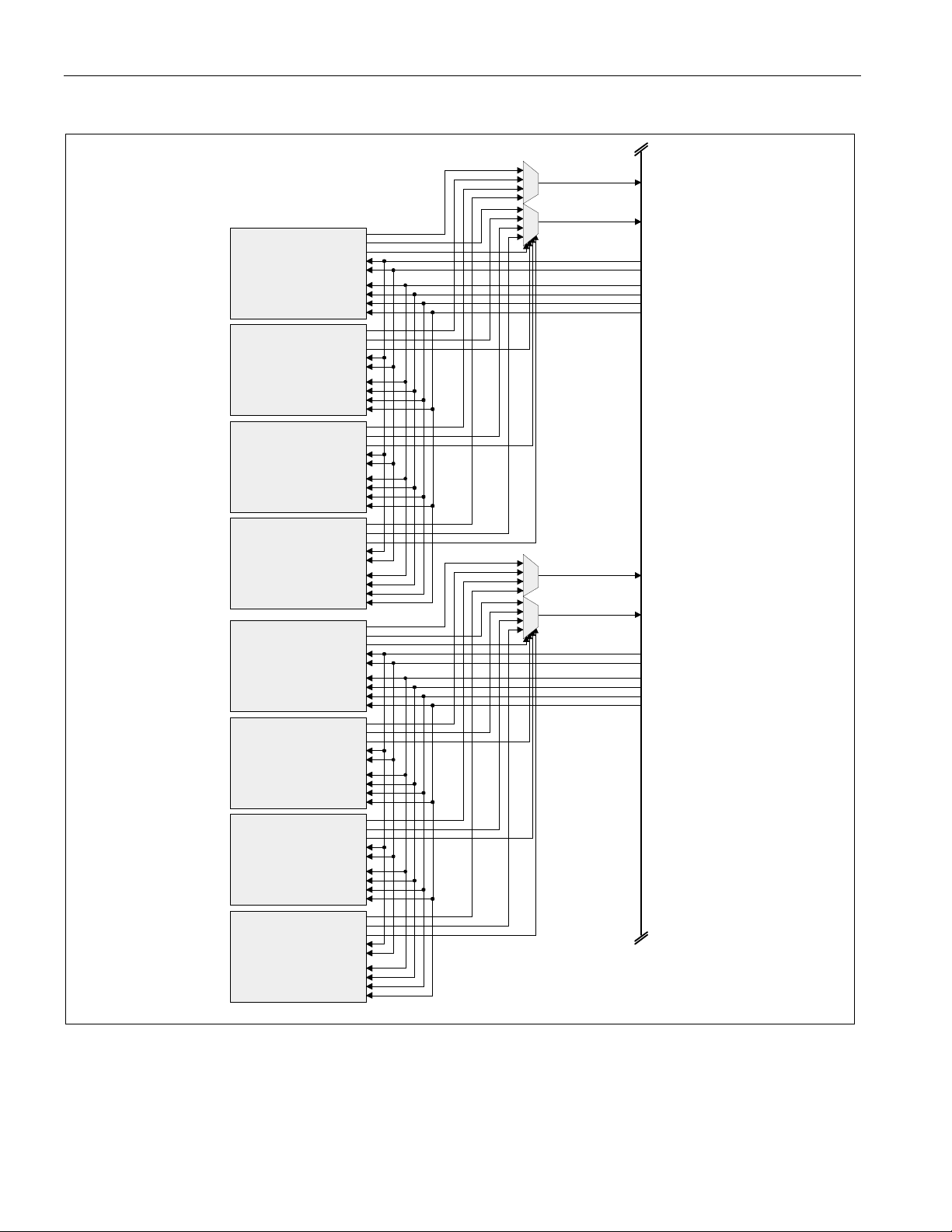
7.3 IBO Multiplexer
The IBO multiplexer is used with the IBO function located within each framer/formatter block (controlled by the
RIBOC and TIBOC registers). When enabled, the IBO multiplexer simplifies user interface by connecting TDM bus
signals internally. The IBO multiplexer eliminates the need for ganged external wiring and tri-state output drivers on
the RSER and RSIG pins.
The DS26401 also supports the traditional mode of IBO operation by allowing complete access to individual framers
and tri-stating the RSER and RSIG pins at the appropriate times for external bus wiring. This operation mode is
enabled per framer in the associated RIBOC and TIBOC registers, while leaving the IBO multiplexer disabled
(IBOMS0 = 0 and IBOMS1 = 0).
Figure 7-1
the pin function changes for each mode of the IBO multiplexer.
The transmit and receive IBO functions are described in Sections 8.21
and 11.19
, Figure 7-2, and Figure 7-3 show the equivalent internal circuit for each IBO mode. Table 7-1 describes
(E1 REC).
(T1 XMIT), 9.20 (T1 REC), 10.17 (E1 XMIT),
27
Page 28
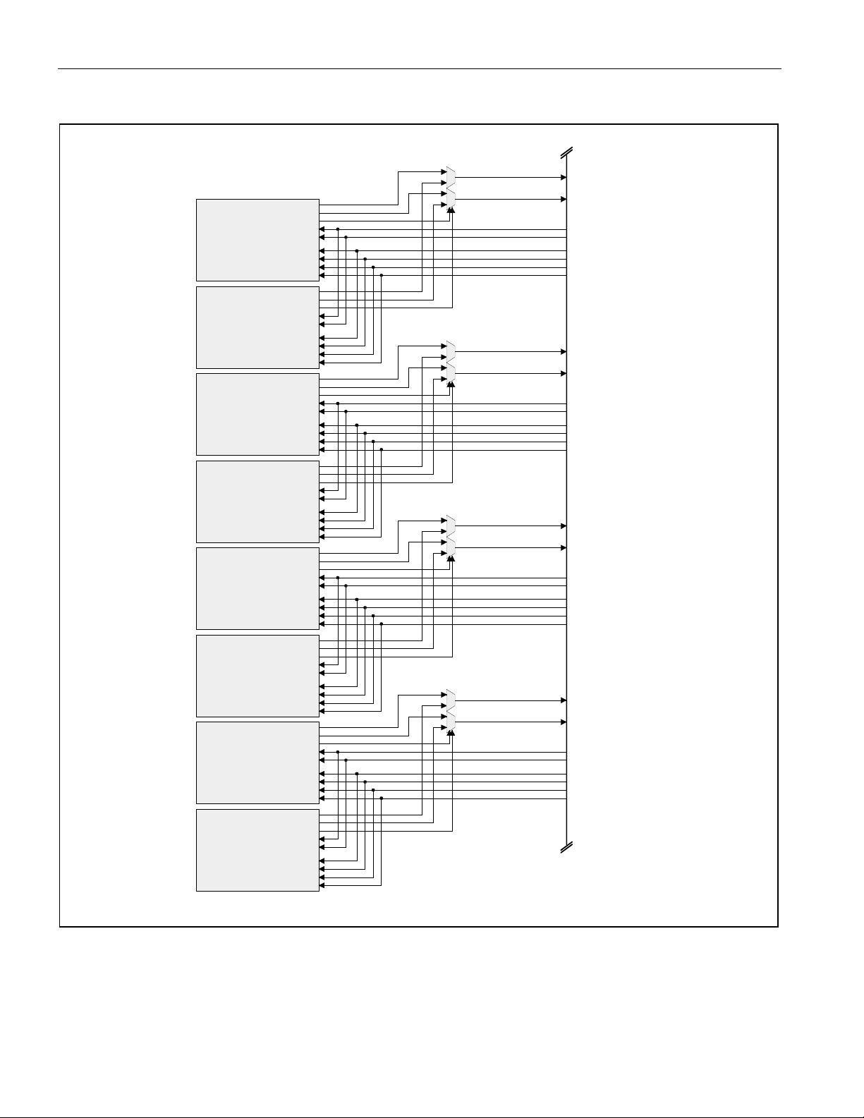
DS26401 Octal T1/E1/J1 Framer
Figure 7-1. Internal IBO Multiplexer Equivalent Circuit—4.096MHz
RSER1
RSIG1
RSYNC1
RSYSCLK1
TSER1
TSIG1
TSSYNC1
TSYSCLK1
RSER3
RSIG3
RSYNC3
RSYSCLK3
TSER3
TSIG3
TSSYNC3
TSYSCLK3
RSER5
RSIG5
RSYNC5
RSYSCLK5
TSER5
TSIG5
TSSYNC5
TSYSCLK5
RSER7
RSIG7
RSYNC7
RSYSCLK7
TSER7
TSIG7
TSSYNC7
TSYSCLK7
Port # 1
Backplane
Interface
Port # 2
Backplane
Interface
Port # 3
Backplane
Interface
Port # 4
Backplane
Interface
Port # 5
Backplane
Interface
Port # 6
Backplane
Interface
Port # 7
Backplane
Interface
Port # 8
Backplane
Interface
RSER
RSIG
RIBO_OEB
RSYNC
RSYSCLK
TSER
TSIG
TSSYNC
TSYSCLK
RSER
RSIG
RIBO_OEB
RSYNC
RSYSCLK
TSER
TSIG
TSSYNC
TSYSCLK
RSER
RSIG
RIBO_OEB
RSYNC
RSYSCLK
TSER
TSIG
TSSYNC
TSYSCLK
RSER
RSIG
RIBO_OEB
RSYNC
RSYSCLK
TSER
TSIG
TSSYNC
TSYSCLK
RSER
RSIG
RIBO_OEB
RSYNC
RSYSCLK
TSER
TSIG
TSSYNC
TSYSCLK
RSER
RSIG
RIBO_OEB
RSYNC
RSYSCLK
TSER
TSIG
TSSYNC
TSYSCLK
RSER
RSIG
RIBO_OEB
RSYNC
RSYSCLK
TSER
TSIG
TSSYNC
TSYSCLK
RSER
RSIG
RIBO_OEB
RSYNC
RSYSCLK
TSER
TSIG
TSSYNC
TSYSCLK
28
Page 29
DS26401 Octal T1/E1/J1 Framer
Figure 7-2. Internal IBO Multiplexer Equivalent Circuit—8.192MHz
RSER1
Port # 1
Backplane
Interface
Port # 2
Backplane
Interface
Port # 3
Backplane
Interface
Port # 4
Backplane
Interface
Port # 5
Backplane
Interface
Port # 6
Backplane
Interface
Port # 7
Backplane
Interface
Port # 8
Backplane
Interface
RSER
RSIG
RIBO_OEB
RSYNC
RSYSCLK
TSER
TSIG
TSSYNC
TSYSCLK
RSER
RSIG
RIBO_OEB
RSYNC
RSYSCLK
TSER
TSIG
TSSYNC
TSYSCLK
RSER
RSIG
RIBO_OEB
RSYNC
RSYSCLK
TSER
TSIG
TSSYNC
TSYSCLK
RSER
RSIG
RIBO_OEB
RSYNC
RSYSCLK
TSSYNC
TSYSCLK
TSER
TSIG
RSER
RSIG
RIBO_OEB
RSYNC
RSYSCLK
TSER
TSIG
TSSYNC
TSYSCLK
RSER
RSIG
RIBO_OEB
RSYNC
RSYSCLK
TSER
TSIG
TSSYNC
TSYSCLK
RSER
RSIG
RIBO_OEB
RSYNC
RSYSCLK
TSER
TSIG
TSSYNC
TSYSCLK
RSER
RSIG
RIBO_OEB
RSYNC
RSYSCLK
TSER
TSIG
TSSYNC
TSYSCLK
RSIG1
RSYNC1
RSYSCLK1
TSER1
TSIG1
TSSYNC1
TSYSCLK1
RSER5
RSIG5
RSYNC5
RSYSCLK5
TSER5
TSIG5
TSSYNC5
TSYSCLK5
29
Page 30
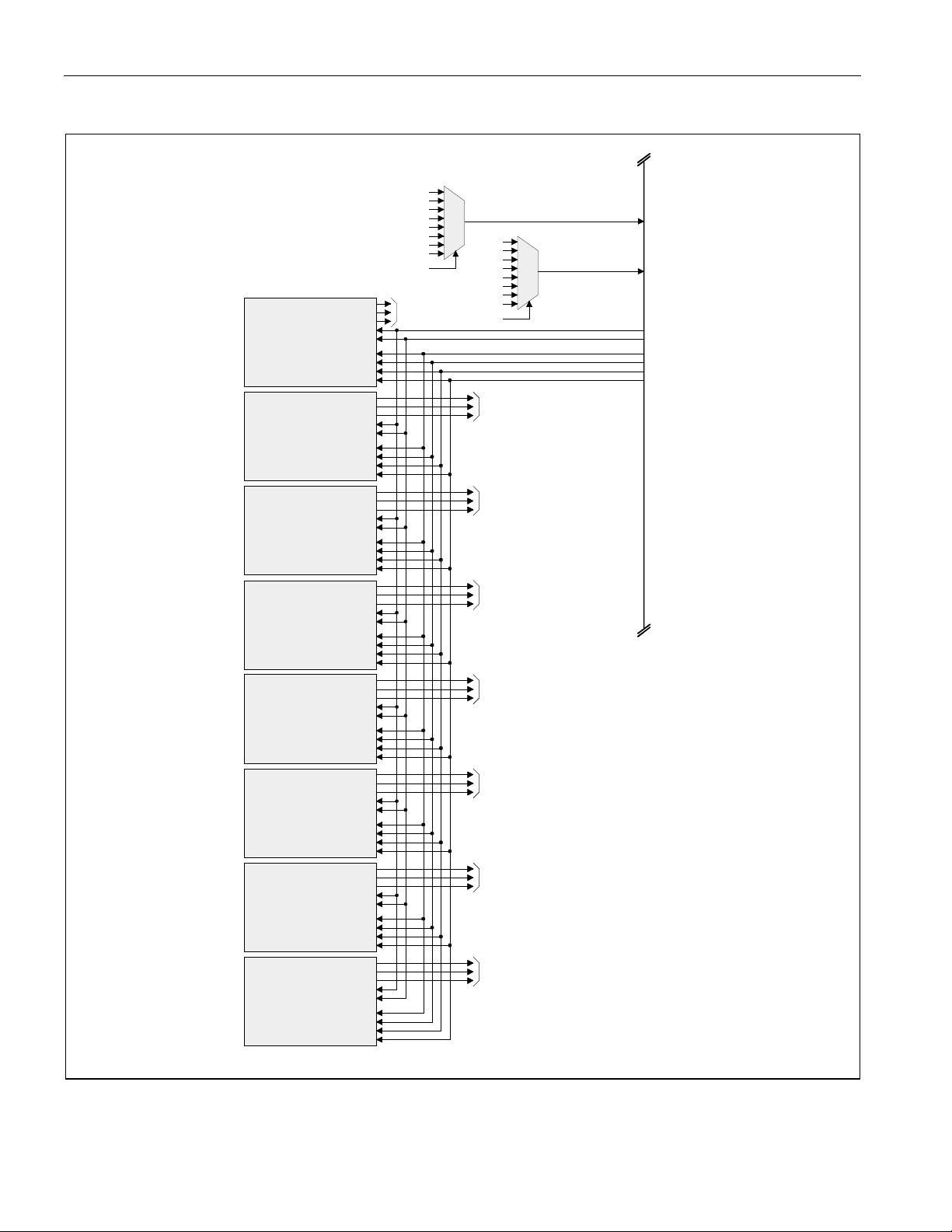
DS26401 Octal T1/E1/J1 Framer
Figure 7-3. Internal IBO Multiplexer Equivalent Circuit—16.394MHz
RSER(1)
RSER(2)
RSER(3)
Port # 1
Backplane
Interface
Port # 2
Backplane
Interface
Port # 3
Backplane
Interface
Port # 4
Backplane
Interface
Port # 5
Backplane
Interface
Port # 6
Backplane
Interface
Port # 7
Backplane
Interface
Port # 8
Backplane
Interface
RSER
RSIG
RIBO_OEB
RSYNC
RSYSCLK
TSER
TSIG
TSSYNC
TSYSCLK
RSER
RSIG
RIBO_OEB
RSYNC
RSYSCLK
TSER
TSIG
TSSYNC
TSYSCLK
RSER
RSIG
RIBO_OEB
RSYNC
RSYSCLK
TSER
TSIG
TSSYNC
TSYSCLK
RSER
RSIG
RIBO_OEB
RSYNC
RSYSCLK
TSER
TSIG
TSSYNC
TSYSCLK
RSER
RSIG
RIBO_OEB
RSYNC
RSYSCLK
TSER
TSIG
TSSYNC
TSYSCLK
RSER
RSIG
RIBO_OEB
RSYNC
RSYSCLK
TSER
TSIG
TSSYNC
TSYSCLK
RSER
RSIG
RIBO_OEB
RSYNC
RSYSCLK
TSER
TSIG
TSSYNC
TSYSCLK
RSER
RSIG
RIBO_OEB
RSYNC
RSYSCLK
TSER
TSIG
TSSYNC
TSYSCLK
RSER(4)
RSER(5)
RSER(6)
RSER(7)
RSER(8)
RIBO_OEB(1-8)
To Mux
RSIG(1)
RSIG(2)
RSIG(3)
RSIG(4)
RSIG(5)
RSIG(6)
RSIG(7)
RSIG(8)
RIBO_OEB(1-8)
To MuxTo Mux
To MuxTo Mux
To MuxTo Mux
To MuxTo Mux
To MuxTo Mux
To MuxTo Mux
To MuxTo Mux
RSER1
RSIG1
RSYNC1
RSYSCLK1
TSER1
TSIG1
TSSYNC1
TSYSCLK1
30
Page 31

DS26401 Octal T1/E1/J1 Framer
Table 7-1. Pin Functions with IBO Mux Enabled
RSER Output Pin Definitions
NAME NORMAL USE 4.096MHz IBO 8.192MHz IBO 16.384MHz IBO
RSER1
RSER2
RSER3
RSER4
RSER5
RSER6
RSER7
RSER8
Rx Serial Data for Port # 1
Rx Serial Data for Port # 2
Rx Serial Data for Port # 3
Rx Serial Data for Port # 4
Rx Serial Data for Port # 5
Rx Serial Data for Port # 6
Rx Serial Data for Port # 7
Rx Serial Data for Port # 8
Combined Rx Serial
Data for Ports 1 & 2
Unused Unused Unused
Combined Rx Serial
Data for Ports 3 & 4
Unused Unused Unused
Combined Rx Serial
Data for Ports 5 & 6
Unused Unused Unused
Combined Rx Serial
Data for Ports 7 & 8
Unused Unused Unused
RSIG Output Pin Definitions
NAME NORMAL USE 4.096MHz IBO 8.192MHz IBO 16.384MHz IBO
RSIG1
RSIG2
RSIG3
RSIG4
RSIG5
RSIG6
RSIG7
RSIG8
Rx Signaling Data for Port # 1
Rx Signaling Data for Port # 2
Rx Signaling Data for Port # 3
Rx Signaling Data for Port # 4
Rx Signaling Data for Port # 5
Rx Signaling Data for Port # 6
Rx Signaling Data for Port # 7
Rx Signaling Data for Port # 8
Combined Rx Signaling
Data for Ports 1 & 2
Unused Unused Unused
Combined Rx Signaling
Data for Ports 3 & 4
Unused Unused Unused
Combined Rx Signaling
Data for Ports 5 & 6
Unused Unused Unused
Combined Rx Signaling
Data for Ports 7 & 8
Unused Unused Unused
Combined Rx Serial
Data for Ports 1–4
Unused Unused
Combined Rx Serial
Data for Ports 5–8
Unused Unused
Combined Rx Signaling
Data for Ports 1–4
Unused Unused
Combined Rx Signaling
Data for Ports 5–8
Unused Unused
Rx Serial Data for
Ports 1–8
Unused
Rx Signaling Data for
Ports 1–8
Unused
31
Page 32

DS26401 Octal T1/E1/J1 Framer
Table 7-1. Pin Functions with IBO Mux Enabled (continued)
TSER Input Pin Definitions
NAME NORMAL USE 4.096MHz IBO 8.192MHz IBO 16.384MHz IBO
TSER1
TSER2
TSER3
TSER4
TSER5
TSER6
TSER7
TSER8
Tx Serial Data for Port # 1
Tx Serial Data for Port # 2
Tx Serial Data for Port # 3
Tx Serial Data for Port # 4
Tx Serial Data for Port # 5
Tx Serial Data for Port # 6
Tx Serial Data for Port # 7
Tx Serial Data for Port # 8
Combined Tx Serial
Data for Ports 1 & 2
Unused Unused Unused
Combined Tx Serial
Data for Ports 3 & 4
Unused Unused Unused
Combined Tx Serial
Data for Ports 5 & 6
Unused Unused Unused
Combined Tx Serial
Data for Ports 7 & 8
Unused Unused Unused
TSIG Input Pin Definitions
NAME NORMAL USE 4.096MHz IBO 8.192MHz IBO 16.384MHz IBO
TSIG1
TSIG2
TSIG3
TSIG4
TSIG5
TSIG6
TSIG7
TSIG8
Tx Signaling Data for Port # 1
Tx Signaling Data for Port # 2
Tx Signaling Data for Port # 3
Tx Signaling Data for Port # 4
Tx Signaling Data for Port # 5
Tx Signaling Data for Port # 6
Tx Signaling Data for Port # 7
Tx Signaling Data for Port # 8
Combined Tx
Signaling Data for
Ports 1 & 2
Unused Unused Unused
Combined Tx
Signaling Data for
Ports 3 & 4
Unused Unused Unused
Combined Tx
Signaling Data for
Ports 5 & 6
Unused Unused Unused
Combined Tx
Signaling Data for
Ports 7 & 8
Unused Unused Unused
Combined Tx Serial
Data for Ports 1–4
Unused Unused
Combined Tx Serial
Data for Ports 5–8
Unused Unused
Combined Tx
Signaling Data for
Ports 1–4
Unused Unused
Combined Tx
Signaling Data for
Ports 5–8
Unused Unused
Tx Serial Data for Ports
Tx Signaling Data for
1–8
Unused
Ports 1–8
Unused
32
Page 33

DS26401 Octal T1/E1/J1 Framer
Table 7-1. Pin Functions with IBO Mux Enabled (continued)
RSYNC Input Pin Definitions
NAME NORMAL USE 4.096MHz IBO 8.192MHz IBO 16.384MHz IBO
RSYNC1
RSYNC2
RSYNC3
RSYNC4
RSYNC5
RSYNC6
RSYNC7
RSYNC8
Rx Frame Pulse for port # 1
Rx Frame Pulse for port # 2
Rx Frame Pulse for port # 3
Rx Frame Pulse for port # 4
Rx Frame Pulse for port # 5
Rx Frame Pulse for port # 6
Rx Frame Pulse for port # 7
Rx Frame Pulse for port # 8
Rx Frame Pulse for
Ports 1 & 2
Unused Unused Unused
Rx Frame Pulse for
Ports 3 & 4
Unused Unused Unused
Rx Frame Pulse for
Ports 5 & 6
Unused Unused Unused
Rx Frame Pulse for
Ports 7 & 8
Unused Unused Unused
TSSYNC Input Pin Definitions
NAME NORMAL USE 4.096MHz IBO 8.192MHz IBO 16.384MHz IBO
TSSYNC1
TSSYNC2
TSSYNC3
TSSYNC4
TSSYNC5
TSSYNC6
TSSYNC7
TSSYNC8
Tx Frame Pulse for Port # 1
Tx Frame Pulse for Port # 2
Tx Frame Pulse for Port # 3
Tx Frame Pulse for Port # 4
Tx Frame Pulse for Port # 5
Tx Frame Pulse for Port # 6
Tx Frame Pulse for Port # 7
Tx Frame Pulse for Port # 8
Tx Frame Pulse for
Ports 1 & 2
Unused Unused Unused
Tx Frame Pulse for
Ports 3 & 4
Unused Unused Unused
Tx Frame Pulse for
Ports 5 & 6
Unused Unused Unused
Tx Frame Pulse for
Ports 7 & 8
Unused Unused Unused
Rx Frame Pulse for
Ports 1–4
Unused Unused
Rx Frame Pulse for
Ports 5–8
Unused Unused
Tx Frame Pulse for
Ports 1– 4
Unused Unused
Tx Frame Pulse for
Ports 5–8
Unused Unused
Rx Frame Pulse for
Ports 1–8
Unused
Tx Frame Pulse for
Ports 1–8
Unused
33
Page 34

DS26401 Octal T1/E1/J1 Framer
Table 7-1. Pin Functions with IBO Mux Enabled (continued)
RSYSCLK Input Pin Definitions
NAME NORMAL USE 4.096MHz IBO 8.192MHz IBO 16.384MHz IBO
RSYSCLK1
RSYSCLK2
RSYSCLK3
RSYSCLK4
RSYSCLK5
RSYSCLK6
RSYSCLK7
RSYSCLK8
Rx System Clock for port # 1
Rx System Clock for port # 2
Rx System Clock for port # 3
Rx System Clock for port # 4
Rx System Clock for port # 5
Rx System Clock for port # 6
Rx System Clock for port # 7
Rx System Clock for port # 8
Rx System Clock for
Ports 1 & 2
Unused Unused Unused
Rx System Clock for
Ports 3 & 4
Unused Unused Unused
Rx System Clock for
Ports 5 & 6
Unused Unused Unused
Rx System Clock for
Ports 7 & 8
Unused Unused Unused
TSYSCLK Input Pin Definitions
NAME NORMAL USE 4.096MHz IBO 8.192MHz IBO 16.384MHz IBO
TSYSCLK1
TSYSCLK2
TSYSCLK3
TSYSCLK4
TSYSCLK5
TSYSCLK6
TSYSCLK7
TSYSCLK8
Tx System Clock for Port # 1
Tx System Clock for Port # 2
Tx System Clock for Port # 3
Tx System Clock for Port # 4
Tx System Clock for Port # 5
Tx System Clock for Port # 6
Tx System Clock for Port # 7
Tx System Clock for Port # 8
Tx System Clock for
Ports 1 & 2
Unused Unused Unused
Tx System Clock for
Ports 3 & 4
Unused Unused Unused
Tx System Clock for
Ports 5 & 6
Unused Unused Unused
Tx System Clock for
Ports 7 & 8
Unused Unused Unused
Rx System Clock for
Ports 1– 4
Unused Unused
Rx System Clock for
Ports 5–8
Unused Unused
Tx System Clock for
Ports 1–4
Unused Unused
Tx System Clock for
Ports 5–8
Unused Unused
Rx System Clock for
Ports 1– 8
Unused
Tx System Clock for
Ports 1– 8
Unused
34
Page 35

DS26401 Octal T1/E1/J1 Framer
Register Name:
Register Description:
Register Address:
IDR
Device Identification Register
0F8h
Bit # 7 6 5 4 3 2 1 0
Name ID7 ID6 ID5 ID4 ID3 ID2 ID1 ID0
Default 0 0 0 0 0 0 0 0
Bits 0 to 3/Chip Revision Bits (ID0 to ID3). The lower four bits of the IDR are used to display the die revision of
the chip. IDO is the LSB of a decimal code that represents the chip revision.
Bits 4 to 7/Device ID (ID4 to ID7). The upper four bits of the IDR are used to display the DS26401 ID.
DEVICE ID (ID4 to ID7)
DS26401 8h
35
Page 36

DS26401 Octal T1/E1/J1 Framer
Register Name:
Register Description:
Register Address:
GSR1
Global Status Register 1
0F9h
Bit # 7 6 5 4 3 2 1 0
Name FIS8 FIS7 FIS6 FIS5 FIS4 FIS3 FIS2 FIS1
Default 0 0 0 0 0 0 0 0
Note: The GSR1 register reports the framer interrupt status for each of the 8 T1/E1 framers. A logic 1 in the associated bit location indicates a
framer has set (active low) its interrupt signal.
Bit 0 / Framer Interrupt Status 1 (FIS1)
0 = Framer 1 has not issued an interrupt
1 = Framer 1 has issued an interrupt
Bit 1 / Framer Interrupt Status 2 (FIS2)
0 = Framer 2 has not issued an interrupt
1 = Framer 2 has issued an interrupt
Bit 2 / Framer Interrupt Status 3 (FIS3)
0 = Framer 3 has not issued an interrupt
1 = Framer 3 has issued an interrupt
Bit 3 / Framer Interrupt Status 4 (FIS4)
0 = Framer 4 has not issued an interrupt
1 = Framer 4 has issued an interrupt
Bit 4 / Framer Interrupt Status 5 (FIS5)
0 = Framer 5 has not issued an interrupt
1 = Framer 5 has issued an interrupt
Bit 5 / Framer Interrupt Status 6 (FIS6)
0 = Framer 6 has not issued an interrupt
1 = Framer 6 has issued an interrupt
Bit 6 / Framer Interrupt Status 7 (FIS7)
0 = Framer 7 has not issued an interrupt
1 = Framer 7 has issued an interrupt
Bit 7 / Framer Interrupt Status 8 (FIS8)
0 = Framer 8 has not issued an interrupt
1 = Framer 8 has issued an interrupt
36
Page 37

DS26401 Octal T1/E1/J1 Framer
—
Register Name:
Register Description:
Register Address:
GSR2
Global Status Register 2
0FAh
Bit # 7 6 5 4 3 2 1 0
Name — —
— — — — BBED BLOS
Default 0 0 0 0 0 0 0 0
Bit 0 / BERT Loss-of-Sync Interrupt Status (BLOS)
0 = The BERT has not issued an interrupt for LOS
1 = The BERT has issued an interrupt for LOS (only possible when BLOSIM in GCR1 is set)
Bit 1 / BERT Bit-Error-Detect Interrupt Status (BBED)
0 = The BERT has not issued an interrupt for BED
1 = The BERT has issued an interrupt for BED (only possible when BBEDIM in GCR1 is set)
Bits 2–7 / Unused
7.4 Interrupt Tree
When the host processor detects an interrupt, the user can first read the GSR1 and GSR2 registers to narrow down
the potential source of the interrupt event. Bit locations set in the GSR1 register direct the user to one or more
framers, from where the appropriate status register(s) can be discerned with RIIR and TIIR.
GSR1 (0F9h)
FIS8 FIS7 FIS6 FIS5 FIS4 FIS3 FIS2 FIS1
E9Fh
F9Fh
To Framer(n) Latched Status Registers
RIIR (09Fh)
NOTE: RLS2 IS NOT USED IN T1 MODE; RLS7 IS NOT USED IN E1 MODE.
C9Fh
D9Fh
A9Fh
B9Fh
89Fh
99Fh
69Fh
79Fh
49Fh
59Fh
29Fh
39Fh
RLS2RLS3 RLS4 RLS5 RLS6 RLS7
INTERRUPT
GSR2 (0FAh)
TIIR (19Fh)
RLS1
Framer for Port #1 (A11:A9 = 000b)
BLOSBBED
BSR (2F4h)
TLS2 TLS1
37
Page 38

DS26401 Octal T1/E1/J1 Framer
8. T1 RECEIVER
8.1 T1 Receiver Register Map
ADDRESS R/W FUNCTION NAME PAGE
000 — Unused (See note) — —
001 — Unused — —
002 — Unused — —
003 — Unused — —
004 — Unused — —
005 — Unused — —
006 — Unused — —
007 — Unused — —
008 — Unused — —
009 — Unused — —
00A — Unused — —
00B — Unused — —
00C — Unused — —
00D — Unused — —
00E — Unused — —
00F — Unused — —
010 R/W Rx HDLC Control RHC 200
011 R/W Rx HDLC Bit Suppress RHBSE 200
012 R/W Rx DS0 Monitor Select RDS0SEL 181
013 R/W Rx Signaling Control RSIGC 184
014 R/W Rx Control 2 RCR2 159
015 R/W Rx BOC Control RBOCC 83
016 — Unused — —
017 — Unused — —
018 — Unused — —
019 — Unused — —
01A — Unused — —
01B — Unused — —
01C R/W Rx Test Register 1 RTEST1 —
01D R/W Rx Test Register 2 RTEST2 —
01E R/W Rx Test Register 3 RTEST3 —
01F R/W Rx Test Register 4 RTEST4 —
020 R/W Rx Idle Definition 1 RIDR1 187
021 R/W Rx Idle Definition 2 RIDR2 187
022 R/W Rx Idle Definition 3 RIDR3 187
023 R/W Rx Idle Definition 4 RIDR4 187
024 R/W Rx Idle Definition 5 RIDR5 187
025 R/W Rx Idle Definition 6 RIDR6 187
026 R/W Rx Idle Definition 7 RIDR7 187
027 R/W Rx Idle Definition 8 RIDR8 187
028 R/W Rx Idle Definition 9 RIDR9 187
029 R/W Rx Idle Definition 10 RIDR10 187
02A R/W Rx Idle Definition 11 RIDR11 187
02B R/W Rx Idle Definition 12 RIDR12 187
02C R/W Rx Idle Definition 13 RIDR13 187
02D R/W Rx Idle Definition 14 RIDR14 187
02E R/W Rx Idle Definition 15 RIDR15 187
02F R/W Rx Idle Definition 16 RIDR16 187
030 R/W Rx Idle Definition 17 RIDR17 187
031 R/W Rx Idle Definition 18 RIDR18 187
032 R/W Rx Idle Definition 19 RIDR19 187
033 R/W Rx Idle Definition 20 RIDR20 187
034 R/W Rx Idle Definition 21 RIDR21 187
035 R/W Rx Idle Definition 22 RIDR22 187
036 R/W Rx Idle Definition 23 RIDR23 187
38
Page 39

DS26401 Octal T1/E1/J1 Framer
ADDRESS R/W FUNCTION NAME PAGE
037 R/W Rx Idle Definition 24 RIDR24 187
038 R/W Rx Sig All Ones Insertion 1 RSAOI1 75
039 R/W Rx Sig All Ones Insertion 2 RSAOI2 75
03A R/W Rx Sig All Ones Insertion 3 RSAOI3 75
03B — Unused — —
03C R/W Rx Digital Milliwatt Enable 1 RDMWE1 63
03D R/W Rx Digital Milliwatt Enable 2 RDMWE2 63
03E R/W Rx Digital Milliwatt Enable 3 RDMWE3 63
03F — Unused — —
040 R Rx Signaling 1 RS1 185
041 R Rx Signaling 2 RS2 185
042 R Rx Signaling 3 RS3 185
043 R Rx Signaling 4 RS4 185
044 R Rx Signaling 5 RS5 185
045 R Rx Signaling 6 RS6 185
046 R Rx Signaling 7 RS7 185
047 R Rx Signaling 8 RS8 185
048 R Rx Signaling 9 RS9 185
049 R Rx Signaling 10 RS10 185
04A R Rx Signaling 11 RS11 185
04B R Rx Signaling 12 RS12 185
04C — Unused — —
04D — Unused — —
04E — Unused — —
04F — Unused — —
050 R Rx Line-Code Violation Counter 1 LCVCR1 66
051 R Rx Line-Code Violation Counter 2 LCVCR2 66
052 R Rx Path-Code Violation Count 1 PCVCR1 67
053 R Rx Path-Code Violation Count 2 PCVCR2 67
054 R Rx Frames Out-of-Sync Counter 1 FOSCR1 68
055 R Rx Frames Out-of-Sync Counter 2 FOSCR2 68
056 — Unused — —
057 — Unused — —
058 — Unused — —
059 — Unused — —
05A — Unused — —
05B — Unused — —
05C — Unused — —
05D — Unused — —
05E — Unused — —
05F — Unused — —
060 R Rx DS0 Monitor RDS0M 181
061 — Unused — —
062 R Rx FDL RFDL 86
063 R Rx BOC RBOC 84
064 R Rx SLC96 Data Link 1 RSLC1 85
065 R Rx SLC96 Data Link 2 RSLC2 85
066 R Rx SLC96 Data Link 3 RSLC3 85
067 — Unused — —
068 — Unused — —
069 — Unused — —
06A — Unused — —
06B — Unused — —
06C — Unused — —
06D — Unused — —
06E — Unused — —
06F — Unused — —
070 — Unused — —
071 — Unused — —
072 — Unused — —
073 — Unused — —
39
Page 40

DS26401 Octal T1/E1/J1 Framer
ADDRESS R/W FUNCTION NAME PAGE
074 — Unused — —
075 — Unused — —
076 — Unused — —
077 — Unused — —
078 — Unused — —
079 — Unused — —
07A — Unused — —
07B — Unused — —
07C — Unused — —
07D — Unused — —
07E — Unused — —
07F — Unused — —
080 R/W Rx Master Mode RMMR 156
081 R/W Rx Control 1 RCR1 158
082 R/W Rx In-Band Code Control RIBCC 87
083 R/W Rx Control 3 RCR3 160
084 R/W Rx I/O Configuration RIOCR 161
085 R/W Rx Elastic Store Control RESCR 190
086 R/W Rx Error Count Configuration ERCNT 65
087 R/W Rx HDLC FIFO Control RHFC 201
088 R/W Rx Interleave Bus Op Control RIBOC 209
089 R/W Rx Spare Code Control RSCC 90
08A R/W Rx BERT Interface Control RBICR 210
08B R/W Rx BERT Bit Suppress En RBBS 211
08C — Unused — —
08D — Unused — —
08E R/W Rx Test Register 5 RTEST5 —
08F R/W Rx Test Register 6 RTEST6 —
090 R/W Rx Latched Status 1 RLS1 166
091 R/W Rx Latched Status 2 RLS2 168
092 R/W Rx Latched Status 3 RLS3 170
093 R/W Rx Latched Status 4 RLS4 173
094 R/W Rx Latched Status 5 RLS5 205
095 — Unused — —
096 R/W Rx Latched Status 7 RLS7
097 — Unused — —
098 R/W Rx Signaling CoS Status 1 RSS1 74
099 R/W Rx Signaling CoS Status 2 RSS2 74
09A R/W Rx Signaling CoS Status 3 RSS3 74
09B — Unused — —
09C R/W Rx Spare Code Definition 1 RSPCD1 87
09D R/W Rx Spare Code Definition 2 RSPCD2 87
09E — Unused — —
09F R/W Rx Interrupt Information Reg RIIR 157
0A0 R/W Rx Interrupt Mask Reg 1 RIM1 167
0A1 — Unused — —
0A2 R/W Rx Interrupt Mask Reg 3 RIM3 171
0A3 R/W Rx Interrupt Mask Reg 4 RIM4 174
0A4 R/W Rx Interrupt Mask Reg 5 RIM5 206
0A5 — Unused — —
0A6 R/W Rx Interrupt Mask Reg 7 RIM7
0A7 — Unused — —
0A8 R/W Rx Sig CoS Interrupt Enable 1 RSCSE1 186
0A9 R/W Rx Sig CoS Interrupt Enable 2 RSCSE2 186
0AA R/W Rx Sig CoS Interrupt Enable 3 RSCSE3 186
0AB — Unused — —
0AC R/W Rx Up-Code Definition 1 RUPCD1 88
0AD R/W Rx Up-Code Definition 2 RUPCD2 88
0AE R/W Rx Down-Code Definition 1 RDNCD1 89
0AF R/W Rx Down-Code Definition 2 RDNCD2 89
0B0 R Rx Real-Time Status 1 RRTS1 165
40
Page 41

DS26401 Octal T1/E1/J1 Framer
ADDRESS R/W FUNCTION NAME PAGE
0B1 — Unused — —
0B2 R Rx Real-Time Status 3 RRTS3 169
0B3 — Unused — —
0B4 R Rx Real-Time Status 5 (HDLC) RRTS5 204
0B5 R Rx HDLC Packet Bytes Available RHPBA 202
0B6 R Rx HDLC FIFO RHF 203
0B7 — Unused — —
0B8 — Unused — —
0B9 — Unused — —
0BA — Unused — —
0BB — Unused — —
0BC — Unused — —
0BD — Unused — —
0BE — Unused — —
0BF — Unused — —
0C0 R/W Rx Blank Channel Select 1 RBCS1 191
0C1 R/W Rx Blank Channel Select 2 RBCS2 191
0C2 R/W Rx Blank Channel Select 3 RBCS3 191
0C3 R/W Rx Blank Channel Select 4 RBCS4 191
0C4 R/W Rx Channel Blocking 1 RCBR1 188
0C5 R/W Rx Channel Blocking 2 RCBR2 188
0C6 R/W Rx Channel Blocking 3 RCBR3 188
0C7 R/W Rx Channel Blocking 4 RCBR4 188
0C8 R/W Rx Signaling Insertion 1 RSI1 186
0C9 R/W Rx Signaling Insertion 2 RSI2 186
0CA R/W Rx Signaling Insertion 3 RSI3 186
0CB R/W Rx Signaling Insertion 4 RSI4 186
0CC R/W Rx Gapped Clock Channel Select 1 RGCCS1 193
0CD R/W Rx Gapped Clock Channel Select 2 RGCCS2 193
0CE R/W Rx Gapped Clock Channel Select 3 RGCCS3 193
0CF R/W Rx Gapped Clock Channel Select 4 RGCCS4 193
0D0 R/W Rx Channel Idle Code Enable 1 RCICE1 187
0D1 R/W Rx Channel Idle Code Enable 2 RCICE2 187
0D2 R/W Rx Channel Idle Code Enable 3 RCICE3 187
0D3 — Unused — —
0D4 R/W Rx BERT Channel Select 1 RBCS1 191
0D5 R/W Rx BERT Channel Select 2 RBCS2 191
0D6 R/W Rx BERT Channel Select 3 RBCS3 191
0D7 — Unused — —
0D8 — Unused — —
0D9 — Unused — —
0DA — Unused — —
0DB — Unused — —
0DC — Unused — —
0DD — Unused — —
0DE — Unused — —
0DF — Unused — —
0E0 — Unused — —
0E1 — Unused — —
0E2 — Unused — —
0E3 — Unused — —
0E4 — Unused — —
0E5 — Unused — —
0E6 — Unused — —
0E7 — Unused — —
0E8 — Unused — —
0E9 — Unused — —
0EA — Unused — —
0EB — Unused — —
0EC — Unused — —
0ED — Unused — —
41
Page 42

DS26401 Octal T1/E1/J1 Framer
ADDRESS R/W FUNCTION NAME PAGE
0EE — Unused — —
0EF — Unused — —
0F0 — Used by Global Functions — —
0F1 — Used by Global Functions — —
0F2 — Unused — —
0F3 — Unused — —
0F4 — Unused — —
0F5 — Unused — —
0F6 — Unused — —
0F7 — Unused — —
0F8 — Used by Global Functions — —
0F9 — Used by Global Functions — —
0FA — Used by Global Functions — —
0FB — Unused — —
0FC — Unused — —
0FD — Unused — —
0FE — Unused — —
0FF — Unused — —
Note: All unused addresses should be set to 0.
42
Page 43

DS26401 Octal T1/E1/J1 Framer
8.2 T1 Receive Framer Description and Operation
The DS26401 includes eight fully independent DS1/E1 framers. The framers are designed to interface seamlessly
to the line side through an external LIU. Each framer can be individually programmed to accept AMI, B8ZS, HDB3,
or NRZ data. In T1 mode, each framer supports D4 (SF), ESF, and SLC-96 frame formats, and detects/reports
common alarms such as AIS, RAI, LOS, and OOF, as well as AIS-CI and RAI-CI. Performance monitor counters
are maintained for each port, which report bipolar/line-code violations, F-bit/CRC errors, and number of out-of-sync
multiframes.
Each framer has an HDLC controller that can be mapped into a single time slot, or Sa4 to Sa8 bits (E1 mode), or
the FDL (T1 mode), and has 64-byte FIFO buffers in both the transmit and receive paths.
The HDLC controllers perform the necessary overhead for generating and receiving performance report messages
(PRM) as described in ANSI T1.403 and the messages as described in AT&T TR54016. The HDLC controllers
automatically generate and detect flags; generate and check the CRC checksum; generate and detect abort
sequences and stuff and destuff zeros; and byte align to the data stream. The FIFO buffers are large enough to
allow a full PRM to be received or transmitted without host intervention.
Other features contained within each framer include a BOC detector with programmable code integration and three
independent 16-bit loop-code detectors. Host interface is simplified with status registers optimized for either
interrupt driven or polled environments. In many cases, status bits are reported in both real-time and latched on
change-of-state with separate bits for each
interrupt on the
Backplane interface is simplified with the inclusion of two-frame elastic-store memories in each of the receive and
transmit paths. These buffers can be used to control slips in asynchronous environments, or rate-adapt from
1.544MHz to 2.048MHz. The DS26401 also supports an interleaved backplane operating at 4.096MHz, 8.192MHz,
or 16.384MHz.
INT pin.
state change. Most latched bits can be mapped to generate an external
Additional details about the operation of the DS1 framer are included in the register descriptions in this section.
43
Page 44

DS26401 Octal T1/E1/J1 Framer
8.3 Receive Master-Mode Register
The receive master-mode register (RMMR) controls the initialization of the receive-side framer. The FRM_EN bit
can be left low if the framer for that particular port is not going to be used, putting the circuit in a low-power (sleep)
state.
Register Name:
Register Description:
Register Address:
Bit # 7 6 5 4 3 2 1 0
Name FRM_EN INIT_DONE — — — — SFTRST T1/E1
Default 0 0 0 0 0 0 0 0
Bit 0 / Receiver T1/E1 Mode Select (T1/E1). This bit sets the operating mode for receiver only! This bit must be
set to the desired state before writing INIT_DONE.
0 = T1 operation
1 = E1 operation
Bit 1 / Soft Reset (SFTRST).
the internal processor.
0 = Normal operation
1 = Hold the internal RISC in reset. This bit only affects the receive-side processor.
Bits 2–5 / Unused. Must be set = 0 for proper operation.
Bit 6 / Initialization Done (INIT_DONE).
been written. The host is required to write or clear all RAM based registers (addresses 00H to 7FH) prior to setting
this bit. Once INIT_DONE is set, the internal processor will check the FRM_EN bit. If enabled, the internal
processor continues executing based on the initial configuration.
Bit 7 / Framer Enable (FRM_EN).
0 = Framer disabled (held in low-power state)
1 = Framer enabled (all features active)
RMMR
Receive Master Mode Register
080h + (200h x n) : where n = 0 to 7, for Ports 1 to 8
Level-sensitive processor reset. Should be taken high, then low to reset and initialize
The host (user) must set this bit once the configuration registers have
This bit must be written with the desired value prior to setting INIT_DONE.
8.4 Interrupt Information Register
The interrupt information registers provide an indication of which DS26401 status registers are generating an
interrupt. When an interrupt occurs, the host can read RIIR to quickly identify which of the seven T1 receive status
registers is causing the interrupt(s). The interrupt information register bits clear once the appropriate interrupt has
been serviced and cleared, as long as no other interrupt condition is present in the associated status register.
Status bits that have been masked through the receive-interrupt mask (RIMx) registers are also masked from the
RIIR register.
Register Name:
Register Description:
Register Address:
Bit # 7 6 5 4 3 2 1 0
Name — RLS7 RLS6 RLS5 RLS4 RLS3 RLS2* RLS1
Default 0 0 0 0 0 0 0 0
*RLS2 does not create an interrupt, therefore this bit is not used in T1 mode.
44
RIIR
Receive Interrupt Information Register
9Fh + (200h x n) : where n = 0 to 7, for Ports 1 to 8
Page 45

DS26401 Octal T1/E1/J1 Framer
8.5 T1 Receive Control Registers
These registers provide the primary setup and control of the receive framers.
Register Name:
Register Description:
Register Address:
Bit # 7 6 5 4 3 2 1 0
Name SYNCT RB8ZS RFM ARC SYNCC RJC SYNCE RESYNC
Default 0 0 0 0 0 0 0 0
Bit 0 / Resynchronize (RESYNC).
initiated. Must be cleared and set again for a subsequent resync.
Bit 1 / Sync Enable (SYNCE)
0 = auto resync enabled
1 = auto resync disabled
Bit 2 / Receive Japanese CRC6 Enable (RJC)
0 = use ANSI/AT&T/ITU CRC6 calculation (normal operation)
1 = use Japanese standard JT-G704 CRC6 calculation
Bit 3 / Sync Criteria (SYNCC)
In D4 Framing Mode:
0 = search for Ft pattern, then search for Fs pattern
1 = cross couple Ft and Fs pattern
In ESF Framing Mode:
0 = search for FPS pattern only
1 = search for FPS and verify with CRC6
Bit 4 / Auto Resync Criteria (ARC)
0 = Resync on OOF or LOS event
1 = Resync on OOF only
Bit 5 / Receive Frame Mode Select (RFM)
0 = ESF framing mode
1 = D4 framing mode
Bit 6 / Receive B8ZS Enable (RB8ZS)
0 = B8ZS disabled
1 = B8ZS enabled
Bit 7 / Sync Time (SYNCT)
0 = qualify 10 bits
1 = qualify 24 bits
RCR1
Receive Control Register 1
081h + (200h x n) : where n = 0 to 7, for Ports 1 to 8
When toggled from low to high, a resynchronization of the receive-side framer is
45
Page 46

DS26401 Octal T1/E1/J1 Framer
Register Name:
Register Description:
Register Address:
RCR2
Receive Control Register 2
014h + (200h x n) : where n = 0 to 7, for Ports 1 to 8
Bit # 7 6 5 4 3 2 1 0
Name — — — RSLC96 OOF2 OOF1 RAIIE RD4RM
Default 0 0 0 0 0 0 0 0
Bit 0 / Receive-Side D4 Remote Alarm Select (RD4RM)
0 = zeros in bit 2 of all channels
1 = a one in the S-bit position of frame 12 (J1 Yellow Alarm Mode)
Bit 1 / Receive RAI Integration Enable (RAIIE). The ESF RAI indication can be interrupted for a period not to
exceed 100ms per interruption (T1.403). In ESF mode, setting RAIIE causes the RAI status from the DS26401 to
be integrated for 200ms.
0 = RAI detects when 16 consecutive patterns of 00FF appear in the FDL.
RAI clears when 14 or less patterns of 00FF hex out of 16 possible appear in the FDL.
1 = RAI detects when the condition has been present for greater than 200ms.
RAI clears when the condition has been absent for greater than 200ms.
Bits 2, 3 / Out-of-Frame Select Bits (OOF2, OOF1)
OOF2 OOF1 OUT OF FRAME CRITERIA
0 0 2/4 frame bits in error
0 1 2/5 frame bits in error
1 0 2/6 frame bits in error
1 1 2/6 frame bits in error
Bit 4 / Receive SLC-96 Synchronizer Enable (RSLC96). See Section 8.17.
0 = the SLC-96 synchronizer is disabled
1 = the SLC-96 synchronizer is enable
Bits 5–7 / Unused. Must be set = 0 for proper operation.
46
Page 47

DS26401 Octal T1/E1/J1 Framer
Register Name:
Register Description:
Register Address:
Bit # 7 6 5 4 3 2 1 0
Name IDF — RSERC — — RLB PLB FLB
Default 0 0 0 0 0 0 0 0
Bit 0 / Framer Loopback (FLB)
0 = loopback disabled
1 = loopback enabled
RCR3
Receive Control Register 3
083h + (200h x n) : where n = 0 to 7, for Ports 1 to 8
RPOS
RNEG
TPOS
TNEG
RECEIVE
FRAMER
TRANSMIT
FRAMER
BACKPLANE
I/F
BACKPLANE
I/F
RSER
TSER
FRAMER LOOPBACK
This loopback is useful in testing and debugging applications. In FLB, the DS26401 loops data from the transmit
side back to the receive side. When FLB is enabled, the following occurs:
1) (T1 mode) An unframed all-ones code is transmitted at TPOS and TNEG.
(E1 mode) Normal data is transmitted at TPOS and TNEG.
2) Data at RPOS and RNEG is ignored.
3) All receive-side signals take on timing synchronous with TCLK instead of RCLK.
Bit 1 / Payload Loopback (PLB)
0 = loopback disabled
1 = loopback enabled
RPOS
RNEG
RECEIVE
FRAMER
BACKPLANE
I/F
RSER
TPOS
TNEG
TRANSMIT
FRAMER
BACKPLANE
I/F
TSER
PAYLOAD LOOPBACK
(CAN BE DONE ON A PER-CHANNEL BASIS)
When PLB is enabled, the following occurs:
1) Data is transmitted from the TPOS and TNEG pins synchronous with RCLK instead of TCLK.
2) All the receive-side signals continue to operate normally.
3) The TCHCLK and TCHBLK signals are forced low.
4) Data at the TSER, TDATA, and TSIG pins is ignored.
5) The TLCLK signal becomes synchronous with RCLK instead of TCLK.
47
Page 48

DS26401 Octal T1/E1/J1 Framer
Normally, this loopback is only enabled when ESF framing is being performed, but it can also be enabled in D4
framing applications. In a PLB situation, the DS26401 loops the 192 bits of payload data (with BPVs corrected) from
the receive section back to the transmit section. The FPS framing pattern, CRC6 calculation, and the FDL bits are
not looped back, they are reinserted by the DS26401.
Bit 2 / Remote Loopback (RLB)
0 = loopback disabled
1 = loopback enabled
RPOS
RNEG
TPOS
TNEG
RECEIVE
FRAMER
TRANSMIT
FRAMER
BACKPLANE
I/F
BACKPLANE
I/F
RSER
TSER
REMOTE LOOPBACK
In this loopback, data input through the RPOS and RNEG pins is transmitted back to the TPOS and TNEG pins.
Data continues to pass through the DS26401’s receive-side framer as it would normally, and the data from the
transmit-side formatter is ignored.
Bits 3, 4, 6 / Unused. Must be set = 0 for proper operation.
Bit 5 / RSER Control (RSERC)
0 = Allow RSER to output data as received under all conditions (normal operation)
1 = Force RSER to one under loss-of-frame alignment conditions
Bit 7 / Input Data Format (IDF)
0 = Bipolar data is expected at RPOS and RNEG (either AMI or B8ZS).
1 = NRZ data is expected at RPOS. The BPV counter is disabled and RNEG is ignored by the DS26401.
48
Page 49

DS26401 Octal T1/E1/J1 Framer
Register Name:
Register Description:
Register Address:
RIOCR
Receive I/O Configuration Register
084h + (200h x n) : where n = 0 to 7, for Ports 1 to 8
Bit # 7 6 5 4 3 2 1 0
Name
RCLKINV RSYNCINV H100EN RSCLKM
RSMS RSIO RSMS2 RSMS1
Default 0 0 0 0 0 0 0 0
Bit 0 / RSYNC Mode Select 1 (RSMS1). Selects frame or multiframe pulse when RSYNC pin is in output mode. In
input mode (elastic store must be enabled) multiframe mode is only useful when receive signaling reinsertion is
enabled.
0 = frame mode
1 = multiframe mode
Bit 1 / RSYNC Mode Select 2 (RSMS2)
T1: RSYNC pin must be programmed in the output frame mode
0 = do not pulse double wide in signaling frames
1 = do pulse double wide in signaling frames
E1: RSYNC pin must be programmed in the output multiframe mode
0 = RSYNC outputs CAS multiframe boundaries
1 = RSYNC outputs CRC4 multiframe boundaries
Bit 2 / RSYNC I/O Select (RSIO). (Note: This bit must be set to zero when elastic store is disabled)
0 = RSYNC is an output
1 = RSYNC is an input (only valid if elastic store enabled)
Bit 3 / RSYNC Multiframe Skip Control (RSMS).
This bit is useful in framing format conversions from D4 to ESF.
This function is not available when the receive-side elastic store is enabled. RSYNC must be set to output
multiframe pulses.
0 = RSYNC outputs a pulse at every multiframe.
1 = RSYNC outputs a pulse at every other multiframe.
Bit 4 / RSYSCLK Mode Select (RSCLKM)
0 = if RSYSCLK is 1.544MHz
1 = if RSYSCLK is 2.048MHz or IBO enabled
Bit 5 / H.100 SYNC Mode (H100EN). See additional details in Section 8.6.
0 = Normal operation
1 = RSYNC and TSSYNC signals are shifted.
Bit 6 / RSYNC Invert (RSYNCINV)
0 = No inversion
1 = Invert RSYNC output
Bit 7 / RCLK Invert (RCLKINV)
0 = No inversion
1 = Invert RCLK as input
49
Page 50

DS26401 Octal T1/E1/J1 Framer
8.6 H.100 (CT Bus) Compatibility
The H.100 (or CT Bus) is a synchronous, bit-serial, TDM transport bus operating at 8.192MHz. The H.100 standard
also allows compatibility modes to operate at 2.048MHz, 4.096MHz, or 8.192MHz. The control bit H100EN
(RIOCR.5), when combined with RSYNCINV and TSSYNCINV, allows the DS26401 to accept a CT-Bus-compatible
frame-sync signal (
CT_FRAME) at the RSYNC and TSSYNC inputs. The following rules apply to the H100EN
control bit:
1) The H100EN bit controls the sampling point for the RSYNC (input mode) and TSSYNC only. (The RSYNC
output and other sync signals are not affected.)
2) The H100EN bit is always used with the receive and transmit elastic store buffers.
3) The H100EN bit is typically used with 8.192MHz IBO mode (Section 8.21
), but can also be used with 4.096MHz
IBO mode or 2.048MHz backplane operation.
4) The H100EN bit in RIOCR controls both RSYNC and TSSYNC (i.e., there is no separate control bit for the
TSSYNC).
5) The H100EN bit does
not invert the expected signal; RSYNCINV (RIOCR) and TSSYNCINV (TIOCR) must be
set high to invert the inbound sync signals.
Figure 8-1. RSYNC Input in H.100 (CT Bus) Mode
RSYNC
RSYNC
1
2
RSYSCLK
RSER
NOTE 1: RSYNC INPUT MODE, IN NORMAL OPERATION
NOTE 2: RSYNC INPUT MODE, H100EN = 1 AND RSYNCINV = 1.
NOTE 3: t
(BIT CELL TIME) = 122ns (typ). tbc = 244ns OR 488ns ALSO ACCEPTABLE.
bc
Bit 8Bit 1Bit 2
3
t
bc
50
Page 51

Figure 8-2. TSSYNC Input in H.100 (CT Bus) Mode
TSSYNC
TSSYNC
TSYSCLK
1
2
DS26401 Octal T1/E1/J1 Framer
TSER
NOTE 1: TSSYNC IN NORMAL OPERATION.
NOTE 2. TSSYNC WITH H100EN = 1 AND TSSYNCINV = 1.
NOTE 3: t
(BIT CELL TIME) = 122ns (typ). tbc = 244ns OR 488ns ALSO ACCEPTABLE.
bc
Bit 8 Bit 1 Bit 2
3
t
bc
51
Page 52

DS26401 Octal T1/E1/J1 Framer
8.7 T1 Receive Status and Information
When a particular event has occurred (or is occurring), the appropriate bit in one of these registers is set to 1.
Status bits can operate in either a latched or real-time fashion. Some latched bits can be enabled to generate a
hardware interrupt through the
Real-Time Bits
Some status bits operate in a real-time fashion. These bits are read-only and indicate the present state of an alarm
or a condition. Real-time bits remain stable and valid during the host read operation. The current value of the
internal status signals can be read at any time from the real-time status registers without changing any of the
latched status register bits.
Latched Bits
When an event or an alarm occurs and a latched bit is set to 1, it remains set until the user clears it. These bits
typically respond on a change-of-state for an alarm, condition, or event, and operate in a read-then-write fashion.
The user should read the value of the desired status bit and then write a 1 to that particular bit location to clear the
latched value (write a zero to locations not to be cleared). Once the bit is cleared, it is not set again until the event
has occurred again.
Mask Bits
Some of the alarms and events can be either masked or unmasked from the interrupt pin through the interrupt
mask registers (RIMx). When unmasked, the
The
INT pin is allowed to return high (if no other unmasked interrupts are present) when the user reads, then clears
(with a write) the alarm bit that caused the interrupt to occur. Note that the latched status bit and the
even if the alarm is still present.
INT signal.
INT signal is forced low when the enabled event or condition occurs.
INT pin clear
Note that some conditions can have multiple status indications. For example, receive loss-of-frame (RLOF)
provides the following indications:
Real-time indication that the receiver is not
RRTS1.0
(RLOF)
RLS1.0
(RLOFD)
RLS1.4
(RLOFC)
synchronized with incoming data stream. Read-only
bit that remains high as long as the condition is
present.
Latched indication that the receiver has lost
synchronization since the bit was last cleared. Bit will
clear when written by the user, even if the condition
is still present (rising edge detect of RRTS1.0).
Latched indication that the receiver has reacquired
synchronization since the bit was last cleared. Bit will
clear when written by the user, even if the condition
is still present (falling edge detect of RRTS1.0).
52
Page 53

Table 8-1. T1 Alarm Criteria
ALARM SET CRITERIA CLEAR CRITERIA
DS26401 Octal T1/E1/J1 Framer
AIS (Blue Alarm) (Note 1)
RAI (Yellow Alarm)
1) D4 Bit 2 Mode
(RCR2.0 = 0)
2) D4 12th F-Bit Mode
(RCR2.0 = 1; also referred to
as the Japanese Yellow
Alarm)
3) ESF Mode
LOS (also referred to as
Receive Carrier Loss (RCL))
Note 1: The definition of the Alarm Indication Signal (Blue Alarm) is an unframed all-ones signal. AIS detectors should be able to operate
properly in the presence of a 10E-3 error rate, and they should not falsely trigger on a framed all-ones signal. The AIS alarm criteria in the
DS26401 has been set to achieve this performance. It is recommended that the RAIS bit be qualified with the RLOF bit.
Note 2: The following terms are equivalent:
RAIS = Blue Alarm
RLOS = RCL
RLOF = Loss of Frame
RRAI = Yellow Alarm
When over a 3ms window, 5 or fewer
zeros are received
When bit 2 of 256 consecutive
channels is set to zero for at least
254 occurrences
When the 12th framing bit is set to
one for two consecutive occurrences
When 16 consecutive patterns of
00FF appear in the FDL
When 192 consecutive zeros are
received
When over a 3ms window, 6 or more
zeros are received
When bit 2 of 256 consecutive channels
is set to zero for less than 254
occurrences
When the 12th framing bit is set to zero
for two consecutive occurrences
When 14 or less patterns of 00FF hex
out of 16 possible appear in the FDL
When 14 or more ones out of 112
possible bit positions are received
starting with the first one received
Register Name:
Register Description:
Register Address:
RRTS1
Receive Real-Time Status Register 1
0B0h + (200h x n) : where n = 0 to 7, for Ports 1 to 8
Bit # 7 6 5 4 3 2 1 0
Name — — — — RRAI RAIS RLOS RLOF
Default 0 0 0 0 0 0 0 0
All bits in this register are real-time (not latched).
Bit 0 / Receive Loss-of-Frame Condition (RLOF). Set when the DS26401 is not synchronized to the received
data stream.
Bit 1 / Receive Loss-of-Signal Condition (RLOS). Set when 192 consecutive zeros have been detected at RPOS
and RNEG.
Bit 2 / Receive Alarm Indication Signal Condition (RAIS). Set when an unframed all-ones code is received at
RPOS and RNEG.
Bit 3 / Receive Remote Alarm Indication Condition (RRAI). Set when a remote alarm is received at RPOS and
RNEG.
Bits 4 to 7 / Unused
53
Page 54

DS26401 Octal T1/E1/J1 Framer
Register Name:
Register Description:
Register Address:
RLS1
Receive Latched Status Register 1
090h + (200h x n) : where n = 0 to 7, for Ports 1 to 8
Bit # 7 6 5 4 3 2 1 0
Name RRAIC RAISC RLOSC RLOFC RRAID RAISD FLOSD RLOFD
Default 0 0 0 0 0 0 0 0
All bits in this register are latched and can create interrupts.
Bit 0 / Receive Loss-of-Frame Condition Detect (RLOFD). Rising edge detect of RLOF. Set when the DS26401
has lost synchronized to the received data stream.
Bit 1 / Receive Loss-of-Signal Condition Detect (RLOSD). Rising edge detect of RLOS. Set when 192
consecutive zeros have been detected at RPOS and RNEG.
Bit 2 / Receive Alarm Indication Signal Condition Detect (RAISD). Rising edge detect of RAIS. Set when an
unframed all-ones code is received at RPOS and RNEG.
Bit 3 / Receive Remote Alarm Indication Condition Detect (RRAID). Rising edge detect of RRAI. Set when a
remote alarm is received at RPOS and RNEG.
Bit 4 / Receive Loss-of-Frame Condition Clear (RLOFC). Falling edge detect of RLOF. Set when an RLOF
condition has cleared.
Bit 5 / Receive Loss-of-Signal Condition Clear (RLOSC). Falling edge detect of RLOS. Set when an RLOS
condition has cleared.
Bit 6 / Receive Alarm Indication Signal Condition Clear (RAISC). Falling edge detect of RAIS. Set when a RAIS
condition has cleared.
Bit 7 / Receive Remote Alarm Indication Condition Clear (RRAIC).
Falling edge detect of RRAI. Set when a
RRAI condition has cleared.
54
Page 55

DS26401 Octal T1/E1/J1 Framer
Register Name:
Register Description:
Register Address:
RIM1
Receive Interrupt Mask Register 1
0A0h + (200h x n) : where n = 0 to 7, for Ports 1 to 8
Bit # 7 6 5 4 3 2 1 0
Name RRAIC RAISC RLOSC RLOFC RRAID RAISD RLOSD RLOFD
Default 0 0 0 0 0 0 0 0
Bit 0 / Receive Loss-of-Frame Condition Detect (RLOFD)
0 = interrupt masked
1 = interrupt enabled
Bit 1 / Receive Loss-of-Signal Condition Detect (RLOSD)
0 = interrupt masked
1 = interrupt enabled
Bit 2 / Receive Alarm Indication Signal Condition Detect (RAISD)
0 = interrupt masked
1 = interrupt enabled
Bit 3 / Receive Remote Alarm Indication Condition Detect (RRAID)
0 = interrupt masked
1 = interrupt enabled
Bit 4 / Receive Loss-of-Frame Condition Clear (RLOFC)
0 = interrupt masked
1 = interrupt enabled
Bit 5 / Receive Loss-of-Signal Condition Clear (RLOSC)
0 = interrupt masked
1 = interrupt enabled
Bit 6 / Receive Alarm Indication Signal Condition Clear (RAISC)
0 = interrupt masked
1 = interrupt enabled
Bit 7 / Receive Remote Alarm Indication Condition Clear (RRAIC)
0 = interrupt masked
1 = interrupt enabled
55
Page 56

DS26401 Octal T1/E1/J1 Framer
Register Name:
Register Description:
Register Address:
RLS2
Receive Latched Status Register 2
091h + (200h x n) : where n = 0 to 7, for Ports 1 to 8
Bit # 7 6 5 4 3 2 1 0
Name RPDV — COFA 8ZD 16ZD SEFE B8ZS FBE
Default 0 0 0 0 0 0 0 0
All bits in this register are latched. This register does not create interrupts.
Bit 0 / Frame Bit Error Event (FBE). Set when an Ft (D4) or FPS (ESF) framing bit is received in error.
Bit 1 / B8ZS Codeword Detect Event (B8ZS). Set when a B8ZS codeword is detected at RPOS and RNEG
independent of whether the B8ZS mode is selected or not. This bit is useful for automatically setting the line coding.
Bit 2 / Severely Errored Framing Event (SEFE). Set when 2 out of 6 framing bits (Ft or FPS) are received in error.
Bit 3 / Sixteen Zero Detect Event (16ZD). Set when a string of at least 16 consecutive zeros (regardless of the
length of the string) have been received at RPOS and RNEG.
Bit 4 / Eight Zero Detect Event (8ZD). Set when a string of at least eight consecutive zeros (regardless of the
length of the string) have been received at RPOS and RNEG.
Bit 5 / Change-of-Frame Alignment Event (COFA). Set when the last resync resulted in a change of frame or
multiframe alignment.
Bit 6 / Unused
Bit 7 / Receive Pulse Density Violation Event (RPDV). Set when the receive data stream does not meet the ANSI
T1.403 requirements for pulse density.
Register Name:
Register Description:
Register Address:
Bit # 7 6 5 4 3 2 1 0
Name — — — — LORC LSP LDN LUP
Default 0 0 0 0 0 0 0 0
All bits in this register are real-time (not latched).
Bit 0 / Loop-Up Code Detected Condition (LUP). Set when the loop-up code as defined in the RUPCD1/2 register
is being received.
Bit 1 / Loop-Down Code Detected Condition (LDN). Set when the loop-down code as defined in the RDNCD1/2
register is being received.
Bit 2 / Spare Code Detected Condition (LSP).
being received.
Bit 3 / Loss-of-Receive Clock Condition (LORC). Set when the RCLK pin has not transitioned for one channel
time.
Bits 4 to 7 / Unused
RRTS3
Receive Real-Time Status Register 3
0B2h + (200h x n) : where n = 0 to 7, for Ports 1 to 8
Set when the spare code as defined in the RSCD1/2 registers is
56
Page 57

DS26401 Octal T1/E1/J1 Framer
Register Name:
Register Description:
Register Address:
RLS3
Receive Latched Status Register 3
092h + (200h x n) : where n = 0 to 7, for Ports 1 to 8
Bit # 7 6 5 4 3 2 1 0
Name LORCC LSPC LDNC LUPC LORCD LSPD LDND LUPD
Default 0 0 0 0 0 0 0 0
All bits in this register are latched and can create interrupts.
Bit 0 / Loop-Up Code Detected Condition Detect (LUPD). Rising edge detect of LUP. Set when the loop-up code
as defined in the RUPCD1/2 register is being received.
Bit 1 / Loop-Down Code Detected Condition Detect (LDND). Rising edge detect of LDN. Set when the loop-
down code as defined in the RDNCD1/2 register is being received.
Bit 2 / Spare Code Detected Condition Detect (LSPD).
Rising edge detect of LSP. Set when the spare code as
defined in the RSCD1/2 registers is being received.
Bit 3 / Loss of Receive Clock Condition Detect (LORCD). Rising edge detect of LORC. Set when the RCLK pin
has not transitioned for one channel time.
Bit 4 / Loop-Up Code Detected Condition Clear (LUPC).
Falling edge detect of LUP. Set when a loop-up
condition was detected and then removed.
Bit 5 / Loop-Down Code Detected Condition Clear (LDNC). Falling edge detect of LDN. Set when a loop-down
condition was detected and then removed.
Bit 6 / Spare Code Detected Condition Clear (LSPC).
Falling edge detect of LSP. Set when a spare-code match
condition was detected and then removed.
Bit 7 / Loss-of-Receive Clock Condition Clear (LORCC). Falling edge detect of LORC. Set when a LORC
condition was detected and then removed.
57
Page 58

DS26401 Octal T1/E1/J1 Framer
Register Name:
Register Description:
Register Address:
RIM3
Receive Interrupt Mask Register 3
0A2h + (200h x n) : where n = 0 to 7, for Ports 1 to 8
Bit # 7 6 5 4 3 2 1 0
Name LORCC LSPC LDNC LUPC LORCD LSPD LDND LUPD
Default 0 0 0 0 0 0 0 0
Bit 0 / Loop-Up Code Detected Condition Detect (LUPD)
0 = interrupt masked
1 = interrupt enabled
Bit 1 / Loop-Down Code Detected Condition Detect (LDND)
0 = interrupt masked
1 = interrupt enabled
Bit 2 / Spare Code Detected Condition Detect (LSPD)
0 = interrupt masked
1 = interrupt enabled
Bit 3 / Loss-of-Receive Clock Condition Detect (LORCD)
0 = interrupt masked
1 = interrupt enabled
Bit 4 / Loop-Up Code Detected Condition Clear (LUPC)
0 = interrupt masked
1 = interrupt enabled
Bit 5 / Loop-Down Code Detected Condition Clear (LDNC)
0 = interrupt masked
1 = interrupt enabled
Bit 6 / Spare Code Detected Condition Clear (LSPC)
0 = interrupt masked
1 = interrupt enabled
Bit 7 / Loss-of-Receive Clock Condition Clear (LORCC)
0 = interrupt masked
1 = interrupt enabled
58
Page 59

DS26401 Octal T1/E1/J1 Framer
Register Name:
Register Description:
Register Address:
RLS4
Receive Latched Status Register 4
093h + (200h x n) : where n = 0 to 7, for Ports 1 to 8
Bit # 7 6 5 4 3 2 1 0
Name RESF RESEM RSLIP — RSCOS 1SEC TIMER RMF
Default 0 0 0 0 0 0 0 0
All bits in this register are latched and can create interrupts.
Bit 0 / Receive Multiframe Event (RMF). Set every 1.5ms on D4 MF boundaries or every 3ms on ESF MF
boundaries.
Bit 1 / Timer Event (TIMER). Follows the error counter update interval as determined by the ECUS bit in the error
counter configuration register (ERCNT).
T1: Set on increments of 1 second or 42ms based on RCLK.
E1: Set on increments of 1 second or 62.5ms based on RCLK.
Bit 2 / One-Second Timer (1SEC).
Set on every one-second interval based on RCLK.
Bit 3 / Receive Signaling Change-of-State Event (RSCOS). Set when any channel selected by the receive
signaling change-of-state interrupt-enable registers (RSCSE1 through RSCSE3), changes signaling state.
Bit 4 / Unused
Bit 5 / Receive Elastic Store Slip Occurrence Event (RSLIP). Set when the receive-elastic store has either
repeated or deleted a frame.
Bit 6 / Receive Elastic Store Empty Event (RESEM). Set when the receive-elastic store buffer empties and a
frame is repeated.
Bit 7 / Receive Elastic Store Full Event (RESF).
Set when the receive-elastic store buffer fills and a frame is
deleted.
59
Page 60

DS26401 Octal T1/E1/J1 Framer
Register Name:
Register Description:
Register Address:
RIM4
Receive Interrupt Mask Register 4
0A3h + (200h x n) : where n = 0 to 7, for Ports 1 to 8
Bit # 7 6 5 4 3 2 1 0
Name RESF RESEM RSLIP — RSCOS 1SEC TIMER RMF
Default 0 0 0 0 0 0 0 0
Bit 0 / Receive Multiframe Event (RMF)
0 = interrupt masked
1 = interrupt enabled
Bit 1 / Timer Event (TIMER)
0 = interrupt masked
1 = interrupt enabled
Bit 2 / One-Second Timer (1SEC)
0 = interrupt masked
1 = interrupt enabled
Bit 3 / Receive Signaling Change-of-State Event (RSCOS)
0 = interrupt masked
1 = interrupt enabled
Bit 4 / Unused. Must be set = 0 for proper operation.
Bit 5 / Receive Elastic Store Slip Occurrence Event (RSLIP)
0 = interrupt masked
1 = interrupt enabled
Bit 6 / Receive Elastic Store Empty Event (RESEM)
0 = interrupt masked
1 = interrupt enabled
Bit 7 / Receive Elastic Store Full Event (RESF)
0 = interrupt masked
1 = interrupt enabled
60
Page 61

DS26401 Octal T1/E1/J1 Framer
Register Name:
Register Description:
Register Address:
RLS7
Receive Latched Status Register 7
096h + (200h x n) : where n = 0 to 7, for Ports 1 to 8
Bit # 7 6 5 4 3 2 1 0
Name — — RRAI-CI RAIS-CI RSLC96 RFDLF BC BD
Default 0 0 0 0 0 0 0 0
All bits in this register are latched and can create interrupts.
Bit 0 / BOC Detect Event (BD). Set when a valid BOC has been detected (with the BOC filter applied)
(Section 11.11)
Bit 1 / BOC Clear Event (BC). Set when a valid BOC is no longer detected (with the disintegration filter applied).
(Section 11.11)
Bit 2 / Receive FDL Register Full Event (RFDLF).
operation, or manual extraction of FDL data bits (Sections 11.12 and 11.13).
Bit 3 / Receive SLC-96 Alignment Event (RSLC96).
fs-bit stream, and the RSLCx registers have data available for retrieval (Section 11.12).
Bit 4 / Receive AIS-CI Detect (RAIS-CI).
Set when an AIS-CI pattern has been detected by the receiver (see
Section 11.5.1). This bit is set only if an AIS condition is being detected (RRTS1.2). This is a latched bit that must
be cleared by the host, and sets again each time the AIS-CI pattern is detected (approximately every 1.2 seconds).
Bit 5 / Receive RAI-CI Detect (RRAI-CI). Set when an RAI-CI pattern has been detected by the receiver (see
Section 11.5.1). This bit is active in ESF-framing mode only, and sets only if an RAI condition is being detected
(RRTS1.3). When the host reads (and clears) this bit, it will set again each time the RAI-CI pattern is detected
(approximately every 1.1 seconds).
Bits 6, 7 / Unused
Set when the 8-bit RFDL register is full. Useful for SLC-96
Set when a valid SLC-96 alignment pattern is detected in the
61
Page 62

DS26401 Octal T1/E1/J1 Framer
Register Name:
Register Description:
Register Address:
RIM7
Receive Interrupt Mask Register 7 (BOC/FDL)
A6h + (200h x n) : where n = 0 to 7, for Ports 1 to 8
Bit # 7 6 5 4 3 2 1 0
Name — — RRAI-CI RAIS-CI RSLC96 RFDLF BC BD
Default 0 0 0 0 0 0 0 0
Bit 0 / BOC Detect Event (BD)
0 = interrupt masked
1 = interrupt enabled
Bit 1 / BOC Clear Event (BC)
0 = interrupt masked
1 = interrupt enabled
Bit 2 / Receive FDL Register Full (RFDLF)
0 = interrupt masked
1 = interrupt enabled
Bit 3 / Receive SLC-96 (RSLC96)
0 = interrupt masked
1 = interrupt enabled
Bit 4 / Receive AIS-CI (RAIS-CI)
0 = interrupt masked
1 = interrupt enabled
Bit 5 / Receive RAI-CI (RRAI-CI)
0 = interrupt masked
1 = interrupt enabled
Bits 6, 7 / Unused. Must be set = 0 for proper operation.
62
Page 63

DS26401 Octal T1/E1/J1 Framer
8.7.1 Receive AIS-CI and RAI-CI Detection
AIS-CI is a repetitive pattern of 1.26 seconds. It consists of 1.11 seconds of an unframed all ones pattern and 0.15
seconds of all ones modified by the AIS-CI signature. The AIS-CI signature is a repetitive pattern 6176 bits in length
in which, if the first bit is numbered bit 0, bits 3088, 3474 and 5790 are logical zeros and all other bits in the pattern
are logical ones (T1.403). AIS-CI is an unframed pattern and therefore is defined for all T1 framing formats. The
RAIS-CI bit is set when the AIS-CI pattern has been detected and RAIS (RRTS1.2) is set. RAIS-CI is a latched bit
and should be cleared by the host when read. RAIS-CI will continue to set approximately every 1.2 seconds that
the condition is present. The host will need to ‘poll’ the bit, in conjunction with the normal AIS indicators to determine
when the condition has cleared.
RAI-CI is a repetitive pattern within the ESF data link with a period of 1.08 seconds. It consists of sequentially
interleaving 0.99 seconds of “00000000 11111111” (right-to-left) with 90ms of “00111110 11111111”. The RRAI-CI
bit is set when a bit-oriented code of “00111110 11111111” is detected while RRAI (RRTS1.3) is set. The RRAI-CI
detector uses the receive BOC filter bits (RBF0 & RBF1) located in RBOCC to determine the integration time for
RAI-CI detection. Like RAIS-CI, the RRAI-CI bit is latched and should be cleared by the host when read. RRAI-CI
will continue to set approximately every 1.1 seconds that the condition is present. The host will need to ‘poll’ the bit,
in conjunction with the normal RAI indicators to determine when the condition has cleared. It may be useful to
enable the 200ms ESF RAI integration time with the RAIIE control bit (RCR2.1) in networks that use RAI-CI.
8.8 T1 Receive-Side Digital Milliwatt Code Generation
Receive-side digital milliwatt code generation involves using the receive-digital milliwatt registers (T1RDMR1/2/3) to
determine which of the 24 T1 channels of the T1 line going to the backplane should be overwritten with a digital
milliwatt pattern. The digital milliwatt code is an 8-byte repeating pattern that represents a 1kHz sine wave
(1E/0B/0B/1E/9E/8B/8B/9E). Each bit in the T1RDMRx registers, represents a particular channel. If a bit is set to 1,
then the receive data in that channel is replaced with the digital milliwatt code. If a bit is set to zero, no replacement
occurs.
Register Name:
Register Description:
Register Address:
CH8 CH7 CH6 CH5 CH4 CH3 CH2 CH1
CH16 CH15 CH14 CH13 CH12 CH11 CH10 CH9
CH24 CH23 CH22 CH21 CH20 CH19 CH18 CH17
Bits 0 to 7 / Receive-Digital Milliwatt Enable for Channels 1 to 24 (CH1 to CH24)
(MSB)
RDMWE1, RDMWE2, RDMWE3
T1 Receive-Digital Milliwatt-Enable Registers
03Ch, 03Dh, 03Eh [+ (200h x n) : where n = 0 to 7, for Ports 1 to 8]
0 = Do not affect the receive data associated with this channel.
1 = Replace the receive data associated with this channel with digital milliwatt code.
(LSB)
RDMWE1
RDMWE2
RDMWE3
63
Page 64

DS26401 Octal T1/E1/J1 Framer
8.9 T1 Error Count Registers
The DS26401 contains three T1 performance counters that are used to accumulate line coding errors, path errors,
and synchronization errors. Counter update options include one-second boundaries, 42ms (T1 mode only), 62.5ms
(E1 mode only), or manually. See the
automatically, the user can use the interrupt from the timer to determine when to read these registers. The line-code
violation count register has the potential to saturate, but the bit error would have to exceed 10E-2 before this would
occur. All other counters roll over.
Several options are available for latching the performance counters:
1) Each framer’s counters are latched independently based on independent one-second interval timers.
2) Each framer’s counters are latched independently based on independent 42ms interval timers.
3) Each framer’s counters are latched independently with a low-to-high transition on the respective MECU control
bit.
4) Counters from selected framers are latched synchronously at the one-second interval supplied by Framer #1.
5) Counters from selected framers are synchronously latched manually with the global counter latch-enable
(GCLE) bit in GCR1.
The following table shows control bit settings in the ERCNT register to support each of the five modes discussed
above.
Control Bit Mode 1 Mode 2 Mode 3 Mode 4 Mode 5
EAMS 0 0 1 0 1
ECUS 0 1 X 0 0
MECU 0 0 0 to 1 0 0
MCUS 0 0 0 0 1
1SECS 0 0 0 1 0
Error Counter Configuration Register (ERCNT) section. When updated
64
Page 65

DS26401 Octal T1/E1/J1 Framer
Register Name:
Register Description:
Register Address:
Bit # 7 6 5 4 3 2 1 0
Name 1SECS MCUS MECU ECUS EAMS FSBE MOSCRF LCVCRF
Default 0 0 0 0 0 0 0 0
Bit 0 / T1 Line-Code Violation Count Register Function Select (LCVCRF)
0 = do not count excessive zeros
1 = count excessive zeros
Bit 1 / Multiframe Out-of-Sync Count Register Function Select (MOSCRF)
0 = count errors in the framing bit position
1 = count the number of out-of-sync multiframes
Bit 2 / PCVCR Fs-Bit Error Report Enable (FSBE)
0 = do not report bit errors in Fs-bit position; only Ft bit position
1 = report bit errors in Fs-bit position as well as Ft bit position
Bit 3 / Error Accumulation Mode Select (EAMS)
0 = ERCNT.4 determines accumulation time (timed update)
1 = ERCNT.5 determines accumulation time (manual update)
Bit 4 / Error Counter Update Select (ECUS)
T1 mode:
0 = Update error counters once a second
1 = Update error counters every 42ms (336 frames)
E1 mode:
0 = Update error counters once a second
1 = Update error counters every 62.5ms (500 frames)
ERCNT
Error Counter Configuration Register
086h + (200h x n) : where n = 0 to 7, for Ports 1 to 8
Bit 5 / Manual Error Counter Update (MECU). When enabled by ERCNT.3, the changing of this bit from 0 to 1
allows the next clock cycle to load the error counter registers with the latest counts and reset the counters. The user
must wait a minimum of 250
Bit 6 / Manual Counter Update Select (MCUS).
be used to allow the GLCE bit in GCR1 to latch all counters. Useful for synchronously latching counters of multiple
framers.
0 = MECU is used to manually latch counters.
1 = GLCE is used to manually latch counters.
Bit 7 / One-Second Select (1SECS).
allows that framer’s counters to latch on the one-second reference from Framer #1.
0 = Use internally generated one-second timer.
1 = Use one-second timer from Framer #1.
ms before reading the error count registers to allow for proper update.
When manual update mode is enabled with EAMS, this bit can
When timed update is enabled by EAMS, setting this bit for a specific framer
65
Page 66

DS26401 Octal T1/E1/J1 Framer
8.9.1 T1 Line-Code Violation Count Register (LCVCR)
T1 code violations are defined as bipolar violations (BPVs) or excessive zeros. If the B8ZS mode is set for the
receive side, then B8ZS codewords are not counted. This counter is always enabled; it is not disabled during
receive loss-of-synchronization (RLOF = 1) conditions. See Table 8-2
for details of exactly what the LCVCRs count.
Table 8-2. T1 Line-Code Violation Counting Options
COUNT EXCESSIVE ZEROS?
(ERCNT.0)
No No BPVs
Yes No BPVs + 16 consecutive zeros
No Yes BPVs (B8ZS codewords not counted)
Yes Yes BPVs + 8 consecutive zeros
B8ZS ENABLED?
(RCR1.6)
WHAT IS COUNTED
IN THE LCVCRs
Register Name:
Register Description:
Register Address:
LCVCR1
Line-Code Violation Count Register 1
050h + (200h x n) : where n = 0 to 7, for Ports 1 to 8
Bit # 7 6 5 4 3 2 1 0
Name LCVC15 LCVC14 LCVC13 LCVC12 LCVC11 LCVC10 LCVC9 LCCV8
Default 0 0 0 0 0 0 0 0
Bits 0 to 7 / Line-Code Violation Counter Bits 8 to 15 (LCVC8 to LCVC15). LCV15 is the MSB of the 16-bit code
violation count.
Register Name:
Register Description:
Register Address:
LCVCR2
Line-Code Violation Count Register 2
051h + (200h x n) : where n = 0 to 7, for Ports 1 to 8
Bit # 7 6 5 4 3 2 1 0
Name LCVC7 LCVC6 LCVC5 LCVC4 LCVC3 LCVC2 LCVC1 LCVC0
Default 0 0 0 0 0 0 0 0
Bits 0 to 7 / Line-Code Violation Counter Bits 0 to 7 (LCVC0 to LCVC7). LCV0 is the LSB of the 16-bit code
violation count
66
Page 67

DS26401 Octal T1/E1/J1 Framer
8.9.2 T1 Path-Code Violation Count Register (PCVCR)
The path-code violation count register records either Ft, Fs, or CRC6 errors in T1 frames. When the receive side of
a framer is set to operate in the T1 ESF framing mode, PCVCR records errors in the CRC6 codewords. When set
to operate in the T1 D4 framing mode, PCVCR counts errors in the Ft framing bit position. Through the ERCNT.2
bit, a framer can be programmed to also report errors in the Fs framing bit position. The PCVCR is disabled during
receive loss-of-synchronization (RLOF = 1) conditions. See Table 8-3
for a detailed description of exactly what
errors the PCVCR counts.
Table 8-3. T1 Path-Code Violation Counting Arrangements
FRAMING MODE COUNT Fs ERRORS?
D4 No Errors in the Ft pattern
D4 Yes Errors in both the Ft & Fs patterns
ESF Don’t Care Errors in the CRC6 codewords
Register Name:
Register Description:
Register Address:
PCVCR1
Path-Code Violation Count Register 1
052h + (200h x n) : where n = 0 to 7, for Ports 1 to 8
WHAT IS COUNTED
IN THE PCVCRs
Bit # 7 6 5 4 3 2 1 0
Name PCVC15 PCVC14 PCVC13 PCVC12 PCVC11 PCVC10 PCVC9 PCVC8
Default 0 0 0 0 0 0 0 0
Bits 0 to 7 / Path-Code Violation Counter Bits 8 to 15 (PCVC8 to PCVC15). PCVC15 is the MSB of the 16-bit
path-code violation count
Register Name:
Register Description:
Register Address:
PCVCR2
Path-Code Violation Count Register 2
053h + (200h x n) : where n = 0 to 7, for Ports 1 to 8
Bit # 7 6 5 4 3 2 1 0
Name PCVC7 PCVC6 PCVC5 PCVC4 PCVC3 PCVC2 PCVC1 PCVC0
Default 0 0 0 0 0 0 0 0
Bits 0 to 7 / Path-Code Violation Counter Bits 0 to 7 (PCVC0 to PCVC7). PCVC0 is the LSB of the 16-bit path-
code violation count.
67
Page 68

DS26401 Octal T1/E1/J1 Framer
8.9.3 T1 Frames Out-of-Sync Count Register (FOSCR)
The FOSCR is used to count the number of multiframes that the receive synchronizer is out of sync. This number is
useful in ESF applications needing to measure the parameters loss-of-frame count (LOFC) and ESF error events
as described in AT&T publication TR54016. When the FOSCR is operated in this mode, it is not disabled during
receive loss of synchronization (RLOF = 1) conditions. The FOSCR has alternate operating mode whereby it will
count either errors in the Ft framing pattern (in the D4 mode) or errors in the FPS framing pattern (in the ESF
mode). When the FOSCR is operated in this mode, it is disabled during receive loss-of-synchronization (RLOF = 1)
conditions. See Table 8-4
for a detailed description of what the FOSCR is capable of counting.
Table 8-4. T1 Frames Out-of-Sync Counting Arrangements
FRAMING MODE
(RCR1.5)
D4 MOS Number of multiframes out of sync
D4 F-Bit Errors in the Ft pattern
ESF MOS Number of multiframes out of sync
ESF F-Bit Errors in the FPS pattern
COUNT MOS OR F–BIT ERRORS
(ERCNT.1)
WHAT IS COUNTED
IN THE FOSCRs
Register Name:
Register Description:
Register Address:
FOSCR1
Frames Out-of-Sync Count Register 1
054h + (200h x n) : where n = 0 to 7, for Ports 1 to 8
Bit # 7 6 5 4 3 2 1 0
Name FOS15 FOS14 FOS13 FOS12 FOS11 FOS10 FOS9 FOS8
Default 0 0 0 0 0 0 0 0
Bits 0 to 7 / Frames Out-of-Sync Counter Bits 8 to 15 (FOS8 to FOS15). FOS15 is the MSB of the 16-bit frames
out-of-sync count.
Register Name:
Register Description:
Register Address:
FOSCR2
Frames Out-of-Sync Count Register 2
055h + (200h x n) : where n = 0 to 7, for Ports 1 to 8
Bit # 7 6 5 4 3 2 1 0
Name FOS7 FOS6 FOS5 FOS4 FOS3 FOS2 FOS1 FOS0
Default 0 0 0 0 0 0 0 0
Bits 0 to 7 / Frames Out-of-Sync Counter Bits 0 to 7 (FOS0 to FOS7). FOS0 is the LSB of the 16-bit frames out-
of-sync count.
68
Page 69

DS26401 Octal T1/E1/J1 Framer
8.10 DS0 Monitoring Function
The DS26401 can monitor one DS0 (64kbps) channel in the transmit direction and one DS0 channel in the receive
direction at the same time. In the receive direction, the RCM0 to RCM4 bits in the RDS0SEL register need to be
properly set and the DS0 channel pointed to by the RCM0 to RCM4 bits will appear in the receive DS0 (RDS0M)
register. The RCM4 to RCM0 bits should be programmed with the decimal decode of the appropriate T1 channel.
T1 channels 1 through 24 map to register values 0 through 23. For example, if DS0 channel 15 in the receive
direction needed to be monitored, then the following values would be programmed into RDS0SEL:
RCM4 = 0
RCM3 = 1
RCM2 = 1
RCM1 = 1
RCM0 = 0
Register Name:
Register Description:
Register Address:
Bit # 7 6 5 4 3 2 1 0
Name — — — RCM4 RCM3 RCM2 RCM1 RCM0
Default 0 0 0 0 0 0 0 0
Bits 0 to 4 / Receive-Channel Monitor Bits (RCM0 to RCM4). RCM0 is the LSB of a 5-bit channel select that
determines which receive-DS0 channel data appears in the RDS0M register.
Bits 5–7 / Unused. Must be set = 0 for proper operation.
Register Name:
Register Description:
Register Address:
Bit # 7 6 5 4 3 2 1 0
Name B1 B2 B3 B4 B5 B6 B7 B8
Default 0 0 0 0 0 0 0 0
Bits 0 to 7 / Receive-DS0 Channel Bits (B1 to B8). Receive-channel data that has been selected by the receive-
channel monitor select register. B8 is the LSB of the DS0 channel (last bit to be received).
RDS0SEL
Receive-Channel Monitor Select
012h + (200h x n) : where n = 0 to 7, for Ports 1 to 8
RDS0M
Receive-DS0 Monitor Register
060h + (200h x n) : where n = 0 to 7, for Ports 1 to 8
69
Page 70

DS26401 Octal T1/E1/J1 Framer
8.11 T1 Receive Signaling Operation
There are two methods to access receive-signaling data: through processor-based (i.e., software-based) signaling
or hardware-based signaling. Processor-based refers to access through the receive-signaling registers, RS1–RS12.
Hardware-based refers to the RSIG pin. Both methods can be used simultaneously.
8.11.1 Processor-Based Signaling
The robbed-bit signalingis sampled in the receive data stream and copied into the receive-signaling registers, RS1
through RS12. The signaling information in these registers is always updated on multiframe boundaries. This
function is always enabled.
8.11.2 Change of State
To avoid constant monitoring of the receive-signaling registers, the DS26401 can be programmed to alert the host
when any specific channel or channels undergo a change of their signaling state. For T1, RSCSE1 through
RSCSE3 are used to select which channels can cause a change-of-state indication. The change of state is
indicated in latched status register 4 (RLS4.3). If signaling integration is enabled, the new signaling state must be
constant for three multiframes before a change-of-state indication is indicated. The user can enable the
toggle low upon detection of a change in signaling by setting the interrupt mask bit RIM4.3. The signaling integration
mode is global and cannot be enabled on a channel-by-channel basis.
The user can identify which channels have undergone a signaling change of state by reading the receive-signaling
status (RSS1–RSS3) registers. The information from these registers tells the user which RSx register to read for
the new signaling data. All changes are indicated in the RSS1–RSS3 registers regardless of the RSCSE1–RSCSE3
registers.
INT pin to
8.11.3 Hardware-Based Receive Signaling
In hardware-based signaling, the signaling data can be obtained from the RSER pin or the RSIG pin. RSIG is a
signaling-PCM stream output on a channel-by-channel basis from the signaling buffer. The T1 robbed-bit signaling
data is still present in the original data stream at RSER. The signaling buffer provides signaling data to the RSIG pin
and also allows signaling data to be reinserted into the original data stream in a different alignment that is
determined by a multiframe signal from the RSYNC pin. In this mode, the receive-elastic store can be enabled or
disabled. If the receive-elastic store is enabled, then the backplane clock (RSYSCLK) can be either 1.544MHz or
2.048MHz. If IBO mode is enabled, then RSYSCLK can also be 4.096MHz, 8.192MHz, or 16.384MHz. In the ESFframing mode, the ABCD signaling bits are output on RSIG in the lower nibble of each channel. The RSIG data is
updated once a multiframe (3ms) unless a freeze is in effect. In the D4 framing mode, the AB signaling bits are
output twice on RSIG in the lower nibble of each channel. Hence, bits 5 and 6 contain the same data as bits 7 and
8, respectively, in each channel. The RSIG data is updated once a multiframe (1.5ms) unless a freeze is in effect.
8.11.4 Signaling Debounce
When signaling integration is enabled, the signaling data at RSIG is automatically debounced. Signaling must be
constant for three multiframes before being updated at RSIG. Signaling debounce is enabled on a global basis.
70
Page 71

DS26401 Octal T1/E1/J1 Framer
8.11.5 Receive-Signaling Reinsertion at RSER
In this mode, the user provides a multiframe sync at the RSYNC pin, and the signaling data is reinserted based on
this alignment. In T1 mode, this results in two copies of the signaling data in the RSER data stream. The original
signaling data is based on the Fs/ESF frame positions and the realigned data is based on the user-supplied
multiframe sync applied at RSYNC. In voice channels, this extra copy of signaling data is of little consequence.
Reinsertion can be avoided in data channels since this feature is activated on a per-channel basis. For reinsertion,
the elastic store must be enabled, however, the backplane clock can be either 1.544MHz or 2.048MHz.
Signaling reinsertion mode is enabled on a per-channel basis by setting the receive-signaling reinsertion channelselect bit high in the RSIx registers. The channels that are to have signaling reinserted are selected by writing to the
RSI1–RSI3 registers for T1.
8.11.6 Force Receive-Signaling All Ones
In T1 mode, the user can, on a per-channel basis, force the robbed-bit signaling bit positions to 1. This is done by
using the RSAOI registers. The user sets the channel-select bit in the RSAOI1–RSAOI3 registers to select the
channels that are to have the signaling forced to 1.
8.11.7 Receive-Signaling Freeze
The signaling data in the four-multiframe signaling buffer is frozen in a known good state upon either a loss-ofsynchronization (OOF event), carrier loss, or change-of-frame alignment. This action meets the requirements of
BellCore TR-TSY-000170 for signaling freezing. To allow this freeze action to occur, the RSFE control bit
(RSIGC.1) should be set high. The user can force a freeze by setting the RSFF control bit (RSIGC.2) high. The
RSIGF output pin provides a hardware indication that a freeze is in effect. The four-multiframe buffer provides a
three-multiframe delay in the signaling bits provided at the RSIG pin (and at the RSER pin if receive-signaling
reinsertion is enabled). When freezing is enabled (RSFE = 1), the signaling data is held in the last known good state
until the corrupting error condition subsides. When the error condition subsides, the signaling data is held in the old
state for at least an additional 9ms (or 4.5ms in D4 framing mode) before being allowed to be updated with new
signaling data.
71
Page 72

DS26401 Octal T1/E1/J1 Framer
Register Name:
Register Description:
Register Address:
RSIGC
Receive Signaling Control Register
013h + (200h x n) : where n = 0 to 7, for Ports 1 to 8
Bit # 7 6 5 4 3 2 1 0
Name — — — RFSA1 — RSFF RSFE RSIE
Default 0 0 0 0 0 0 0 0
Bit 0 / Receive-Signaling Integration Enable (RSIE)
0 = signaling changes of state reported on any change in selected channels
1 = signaling must be stable for three multiframes for a change of state to be reported
Bit 1 / Receive-Signaling Freeze Enable (RSFE)
0 = no freezing of receive-signaling data occurs
1 = allow freezing of receive-signaling data at RSIG (and RSER if receive-signaling reinsertion is enabled)
Bit 2 / Receive-Signaling Force Freeze (RSFF). Freezes receive-side signaling at RSIG (and RSER if receive-
signaling reinsertion is enabled); overrides receive-freeze enable (RFE).
0 = do not force a freeze event
1 = force a freeze event
Bits 3, 5–7 / Unused. Must be set = 0 for proper operation.
Bit 4 / Receive-Force Signaling All Ones (RFSA1)
0 = do not force robbed bit signaling to all ones
1 = force signaling bits to all ones on a per-channel basis according to the RSAOI1–RSAOI3 registers
72
Page 73

DS26401 Octal T1/E1/J1 Framer
Register Name:
Register Description:
Register Address:
RS1 to RS12
Receive Signaling Registers
040h to 04Bh [+ (200h x n) : where n = 0 to 7, for Ports 1 to 8]
In the ESF framing mode, there can be up to four signaling bits per channel (A, B, C, and D). In the D4 framing
mode, there are only two signaling bits per channel (A and B). In the D4 framing mode, the framer repeats the A
and B signaling data in the C and D bit locations. Therefore, when the framer is operated in D4 framing mode, the
user needs to retrieve the signaling bits every 1.5ms as opposed to 3ms for ESF mode. The receive-signaling
registers are frozen and not updated during a loss-of-sync condition. They contain the most recent signaling
information before the OOF occurred.
(MSB)
(LSB)
CH1-A CH1-B CH1-C CH1-D CH13-A CH13-B CH13-C CH13-D
CH2-A CH2-B CH2-C CH2-D CH14-A CH14-B CH14-C CH14-D
CH3-A CH3-B CH3-C CH3-D CH15-A CH15-B CH15-C CH15-D
CH4-A CH4-B CH4-C CH4-D CH16-A CH16-B CH16-C CH16-D
CH5-A CH5-B CH5-C CH5-D CH17-A CH17-B CH17-C CH17-D
CH6-A CH6-B CH6-C CH6-D CH18-A CH18-B CH18-C CH18-D
CH7-A CH7-B CH7-C CH7-D CH19-A CH19-B CH19-C CH19-D
CH8-A CH8-B CH8-C CH8-D CH20-A CH20-B CH20-C CH20-D
CH9-A CH9-B CH9-C CH9-D CH21-A CH21-B CH21-C CH21-D
CH10-A CH10-B CH10-C CH10-D CH22-A CH22-B CH22-C CH22-D
CH11-A CH11-B CH11-C CH11-D CH23-A CH23-B CH23-C CH23-D
CH12-A CH12-B CH12-C CH12-D CH24-A CH24-B CH24-C CH24-D
RS1
RS2
RS3
RS4
RS5
RS6
RS7
RS8
RS9
RS10
RS11
RS12
73
Page 74

DS26401 Octal T1/E1/J1 Framer
Register Name:
Register Description:
Register Address:
RSS1, RSS2, RSS3
Receive Signaling Status Registers
098h, 099h, 09Ah [+ (200h x n) : where n = 0 to 7, for Ports 1 to 8]
When a channel’s signaling data changes state, the respective bit in registers RSS1–RSS3 is set and latched. The
RSCOS bit (RLSR4.3) is set if the channel was also enabled by setting the appropriate bit in RSCSE1–3. The
INT
signal goes low if enabled by the interrupt mask bit RIM4.3.
(MSB)
CH8 CH7 CH6 CH5 CH4 CH3 CH2 CH1
CH16 CH15 CH14 CH13 CH12 CH11 CH10 CH9
CH24 CH23 CH22 CH21 CH20 CH19 CH18 CH17
Note: Status bits in this register are latched.
(LSB)
RSS1
RSS2
RSS3
Register Name:
Register Description:
Register Address:
RSCSE1, RSCSE2, RSCSE3
Receive-Signaling Change-of-State Enable
0A8h, 0A9h, 0AAh [+ (200h x n) : where n = 0 to 7, for Ports 1 to 8]
Setting any of the CH1 through CH24 bits in the RSS1 through RSS3 registers cause RSCOS (RLSR4.3) to be set
when that channel’s signaling data changes state.
(MSB)
CH8 CH7 CH6 CH5 CH4 CH3 CH2 CH1
CH16 CH15 CH14 CH13 CH12 CH11 CH10 CH9
CH24 CH23 CH22 CH21 CH20 CH19 CH18 CH17
(LSB)
RSCSE1
RSCSE2
RSCSE3
74
Page 75

DS26401 Octal T1/E1/J1 Framer
Register Name:
Register Description:
Register Address:
RSI1, RSI2, RSI3, RSI4
Receive-Signaling Reinsertion Enable Registers
0C8h, 0C9h, 0CAh, 0CBh [+ (200h x n) : where n = 0 to 7, for Ports 1
to 8]
Setting any of the CH1 through CH24 bits in the RSI1 through RSI3 registers causes signaling data to be reinserted
for the associated channel. RSI4 is used for 2.048MHz backplane operation.
(MSB)
CH8 CH7 CH6 CH5 CH4 CH3 CH2 CH1
CH16 CH15 CH14 CH13 CH12 CH11 CH10 CH9
CH24 CH23 CH22 CH21 CH20 CH19 CH18 CH17
CH32 CH31 CH30 CH29 CH28 CH27 CH26 CH25
(LSB)
RSI1
RSI2
RSI3
RSI4*
Register Name:
Register Description:
Register Address:
RSAOI1, RSAOI2, RSAOI3,
Receive-Signaling All-Ones Insertion Registers
038h, 039h, 03Ah [+ (200h x n) : where n = 0 to 7, for Ports 1 to 8]
Setting any of the CH1 through CH24 bits in the RSAOI1 through RSAOI3 registers causes signaling data to be
replaced with logic ones as received at the backplane.
(MSB)
CH8 CH7 CH6 CH5 CH4 CH3 CH2 CH1
CH16 CH15 CH14 CH13 CH12 CH11 CH10 CH9
CH24 CH23 CH22 CH21 CH20 CH19 CH18 CH17
(LSB)
RSAOI1
RSAOI2
RSAOI3
75
Page 76

DS26401 Octal T1/E1/J1 Framer
8.12 T1 Receive Per-Channel Idle Code Insertion
Channel data can be replaced by an idle code on a per-channel basis in the transmit and receive directions.
Twenty-four receive idle definition registers (RIDR1–RIDR24) are provided to set the 8-bit idle code for each
channel. The receive-channel idle code-enable registers (RCICE1–3) are used to enable idle code replacement on
a per-channel basis.
Register Name:
Register Description:
Register Address:
Bit # 7 6 5 4 3 2 1 0
Name C7 C6 C5 C4 C3 C2 C1 C0
Default 0 0 0 0 0 0 0 0
Bits 0 to 7 / Per-Channel Idle Code Bits (C0 to C7). C0 is the LSB of the code (this bit is transmitted last).
Address 20H is for channel 1; address 37H is for channel 24.
Register Name:
Register Description:
Register Address:
The receive-channel idle code-enable registers (RCICE1/2/3) are used to determine which of the 24 T1 channels
from the T1 line to the backplane should be overwritten with the code placed in the receive idle-code definition
register.
(MSB)
CH8 CH7 CH6 CH5 CH4 CH3 CH2 CH1
CH16 CH15 CH14 CH13 CH12 CH11 CH10 CH9
CH24 CH23 CH22 CH21 CH20 CH19 CH18 CH17
Bits 0 to 7 / Receive Channels 1 to 24 Code Insertion Control Bits (CH1 to CH24)
0 = do not insert data from the idle code array into the receive data stream
1 = insert data from the idle code array into the receive data stream
RIDR1 to RIDR24
Receive Idle-Code Definition Registers 1 to 24
020h to 037h [+ (200h x n) : where n = 0 to 7, for Ports 1 to 8]
RCICE1, RCICE2, RCICE3
Receive-Channel Idle Code-Enable Registers
0D0h, 0D1h, 0D2h [+ (200h * n) : where n = 0 to 7, for Ports 1 to
8]
(LSB)
RCICE1
RCICE2
RCICE3
76
Page 77

DS26401 Octal T1/E1/J1 Framer
8.13 Receive-Channel Blocking Operation
The receive-channel blocking registers (RCBR1/RCBR2/RCBR3/RCBR4) and the transmit-channel blocking
registers (TCBR1/TCBR2/TCBR3/TCBR4) control the RCHBLK and TCHBLK pins respectively. The RCHBLK and
TCHBLK pins are user-programmable outputs that can be forced high or low during individual channels. These
outputs can be used to block clocks to a USART or LAPD controller in ISDN-PRI applications. When the
appropriate bits are set to 1, the RCHBLK and TCHBLK pin is held high during the entire corresponding channel
time. When used in T1 mode, only RCBR1 to RCBR3 and the LSB of RCBR4 are used.
Register Name:
Register Description:
Register Address:
(MSB)
CH8 CH7 CH6 CH5 CH4 CH3 CH2 CH1
CH16 CH15 CH14 CH13 CH12 CH11 CH10 CH9
CH24 CH23 CH22 CH21 CH20 CH19 CH18 CH17
CH32 CH31 CH30 CH29 CH28 CH27 CH26 CH25/Fbit
Bits 0 to 7 / Receive Channels 1 to 32 Channel Blocking Control Bits (CH1 to CH32).
0 = force the RCHBLK pin to remain low during this channel time
1 = force the RCHBLK pin high during this channel time
In T1 mode, the LSB of RCBR4 determines whether or not the RCHBLK signal pulses high during the F-bit
time:
In this mode RCBR4.1 to RCBR4.7 should be set to 0.
RCBR4.0 = 0, do not pulse RCHBLK during the F-bit
RCBR4.0 = 1, pulse RCHBLK during the F-bit
RCBR1, RCBR2, RCBR3, RCBR4
Receive-Channel Blocking Registers
0C4h, 0C5h, 0C6h, 0C7h [+ (200h x n) : where n = 0 to 7, for Ports
1 to 8]
(LSB)
RCBR1
RCBR2
RCBR3
RCBR4*
77
Page 78

DS26401 Octal T1/E1/J1 Framer
8.14 Receive Elastic Stores Operation
The DS26401 contains dual, two-frame elastic stores—one for the receive direction and one for the transmit
direction. Both elastic stores are fully independent. The transmit- and receive-side elastic stores can be
enabled/disabled independent of each other. Also, each elastic store can interface to either a 1.544MHz or
2.048MHz/4.096MHz/8.192MHz/16.384MHz backplane without regard to the backplane rate for the other elastic
store.
The elastic stores have two main purposes. First, they can be used for rate conversion. When the DS26401 is in the
T1 mode, the elastic stores can rate-convert the T1 data stream to a 2.048MHz backplane. In E1 mode, the elastic
store can rate-convert the E1 data stream to a 1.544MHz backplane. Secondly, they can be used to absorb the
differences in frequency and phase between the T1 or E1 data stream and an asynchronous (i.e., not locked)
backplane clock (which can be 1.544MHz or 2.048MHz). In this mode, the elastic stores manage the rate difference
and perform controlled slips, deleting or repeating frames of data in order to manage the difference between the
network and the backplane.
The elastic stores can also be used to multiplex T1 or E1 data streams into higher backplane rates. This is the
interleave bus option (IBO), which is discussed in Section 8.21
Note that the receive-elastic-store status bits are contained in RLS4 with the associated interrupt bits located in
RIM4. These bits indicate a receive slip event, or when the e-store FIFO is in a full or empty condition. See the
register definition for RLS4 for additional information.
.
78
Page 79

DS26401 Octal T1/E1/J1 Framer
Register Name:
Register Description:
Register Address:
RESCR
Receive Elastic Store Control Register
085h + (200h x n) : where n = 0 to 7, for Ports 1 to 8
Bit # 7 6 5 4 3 2 1 0
Name RDATFMT RGCLKEN — RSZS RESALGN RESR RESMDM RESE
Default 0 0 0 0 0 0 0 0
Note: RGPCKEN and RDATFMT are not associated with the elastic store and are explained in the fractional support section.
Bit 0 / Receive-Elastic-Store Enable (RESE)
0 = elastic store is bypassed
1 = elastic store is enabled
Bit 1 / Receive-Elastic Store Minimum Delay Mode (RESMDM)
0 = elastic stores operate at full two-frame depth
1 = elastic stores operate at 32-bit depth
Bit 2 / Receive-Elastic Store Reset (RESR).
Setting this bit from zero to 1 forces the read pointer into the same
frame that the write pointer is exiting, minimizing the delay through the elastic store. If this command should place
the pointers within the slip zone (see bit 4), then an immediate slip occurs and the pointers move back to opposite
frames. Should be toggled after RSYSCLK has been applied and is stable. Do not leave this bit set HIGH.
Bit 3 / Receive-Elastic Store Align (RESALGN).
Setting this bit from zero to 1 forces the receive-elastic store’s
write/read pointers to a minimum separation of half a frame. No action will be taken if the pointer separation is
already greater or equal to half a frame. If pointer separation is less than half a frame, the command will be
executed and the data will be disrupted. Should be toggled after RSYSCLK has been applied and is stable. Must be
cleared and set again for a subsequent align.
Bit 4 / Receive Slip Zone Select (RSZS). This bit determines the minimum distance allowed between the elastic
store read and write pointers before forcing a controlled slip. This bit is only applies during T1 to E1 or E1 to T1
conversion applications.
0 = force a slip at 9 bytes or less of separation (used for clustered blank channels)
1 = force a slip at 2 bytes or less of separation (used for distributed blank channels)
Bit 5 / Unused. Must be set = 0 for proper operation.
Bit 6 / Receive Gapped Clock Enable (RGCLKEN)
0 = RCHCLK functions normally
1 = Enable gapped bit clock output on RCHCLK
Bit 7 / Receive-Channel Data Format (RDATFMT)
0 = 64kbps (data contained in all 8 bits)
1 = 56kbps (data contained in 7 out of the 8 bits)
79
Page 80

DS26401 Octal T1/E1/J1 Framer
8.14.1 Mapping T1 Channels Onto a 2.048MHz Backplane
Setting the RSCLKM bit in RIOCR.4 enables the receive-elastic store to operate with a 2.048MHz backplane (32
time slots/frame). In this mode, the user can choose which of the backplane channels on RSER receive the T1 data
by programming the receive-blank channel-select registers (RBCS1–4). A logic 1 in the associated bit location
forces RSER high for that backplane channel. Typically, the user wants to program 8 channels to be “blanked.” The
default (power-up) configuration blanks channels 25 to 32, so that the 24 T1 channels are mapped into the first 24
channels of the 2.048MHz backplane. If the user chooses to blank channel 1 (TS0) by setting RBCS1.0 = 1, then
the F-bit is passed into the MSB of TS0 on RSER.
For example, if:
RBCS1 = 01h
RBCS2 = 00h
RBCS3 = 01h
RBCS4 = FCh
Then on RSER:
Channel 1 (MSB) = F-bit
Channel 1 (bits 1–7) = all ones
Channels 2–16 = T1 channels 1–15
Channel 17 = all ones
Channels 18–26 = T1 channels 16–24
Channels 27–32 = all ones
Register Name:
Register Description:
Register Address:
Note that when two or more sequential channels are chosen to be blanked, the receive-slip zone-select bit (RSZS)
should be set to zero. If the blank channels are distributed (such as 1, 5, 9, 13, 17, 21, 25, 29), then the RSZS bit
can be set to 1, which may provide a lower occurrence of slips in certain applications.
(MSB)
CH8 CH7 CH6 CH5 CH4 CH3 CH2 CH1
CH16 CH15 CH14 CH13 CH12 CH11 CH10 CH9
CH24 CH23 CH22 CH21 CH20 CH19 CH18 CH17
CH32 CH31 CH30 CH29 CH28 CH27 CH26 CH25
Bits 0–7 / Receive Blank Channel Select for Channels 1 to 32 (RBCS1-32).
0 = do not blank this channel (channel data is available on RSER)
1 = RSER is forced to all ones for this channel
RBCS1, RBCS2, RBCS3, RBCS4
Receive Blank Channel Select Registers
0C0h, 0C1h, 0C2h, 0C3h [+ (200h x n) : where n = 0 to 7, for Ports 1 to 8]
(LSB)
RBCS1
RBCS2
RBCS3
RBCS4
80
Page 81

DS26401 Octal T1/E1/J1 Framer
8.14.2 Additional Receive-Elastic-Store Information
If the receive-side elastic store is enabled, then the user must provide either a 1.544MHz or 2.048MHz clock at the
RSYSCLK pin. For higher rate system clock applications, see the
Interleaved PCM Bus Option in Section 8.21. The
user has the option of either providing a frame/multiframe sync at the RSYNC pin or having the RSYNC pin provide
a pulse on frame/multiframe boundaries. If signaling reinsertion is enabled, the robbed-bit signaling data is
realigned to the multiframe-sync input on RSYNC. Otherwise, a multiframe-sync input on RSYNC is treated as a
simple frame boundary by the elastic store. The framer always indicated frame boundaries on the network side of
the elastic store through the RFSYNC output, whether the elastic store is enabled or not. Multiframe boundaries are
always indicated through the RMSYNC output. If the elastic store is enabled, RMSYNC outputs the multiframe
boundary on the backplane side of the elastic store. When the device is receiving T1, and the backplane is enabled
for 2.048MHz operation, the RMSYNC signal outputs the T1 multiframe boundaries as delayed through the elastic
store.
If the user selects to apply a 2.048MHz clock to the RSYSCLK pin, then the backplane blank-channel-select
registers (RBCS1–4) can be used to determine which channels have the data output at RSER forced to all ones. If
the user chooses to blank time slot 0, then the F-bit is passed into the MSB of TS0. If the two-frame elastic buffer
either fills or empties, a controlled slip occurs. If the buffer empties, a full frame of data is repeated at RSER, and
the RLS4.5 and RLS4.6 bits are set to 1. If the buffer fills, a full frame of data is deleted, and the RLS4.5 and
RLS4.7 bits are set to 1.
8.14.2.1 Elastic Store Initialization
There are two elastic-store initializations that can be used to improve performance in certain applications—the
elastic-store reset and elastic-store align. Both of these involve the manipulation of the elastic store’s read and write
pointers, and are useful primarily in synchronous applications (RSYSCLK/TSYSCLK are locked to RCLK/TCLK
respectively). The elastic-store reset is used to minimize the delay through the elastic store. The elastic-store align
bit is used to center the read/write pointers to the extent possible.
Elastic Store Delay After Initialization
INITIALIZATION REGISTER BIT
Receive-Elastic-Store Reset RESCR.2 N bytes < Delay < 1 Frame + N bytes
Transmit-Elastic-Store Reset TESCR.2 N bytes < Delay < 1 Frame + N bytes
DELAY
Receive-Elastic-Store Align RESCR.3 1/2 Frame < Delay < 1 ½ Frames
Transmit-Elastic-Store Align TESCR.3 1/2 Frame < Delay < 1 ½ Frames
N = 9 for RSZS = 0
N = 2 for RSZS = 1
8.14.2.2 Minimum-Delay Mode
Elastic-store minimum-delay mode can be used when the elastic store’s system clock is locked to its network clock
(i.e., RCLK locked to RSYSCLK for the receive side and TCLK locked to TSYSCLK for the transmit side). RESCR.1
enables the receive-elastic-store minimum-delay mode. When enabled, the elastic stores are forced to a maximum
depth of 32 bits instead of the normal two-frame depth. This feature is useful primarily in applications that interface
to a 2.048MHz bus. Certain restrictions apply when minimum-delay mode is used. In addition to the restriction
mentioned above, RSYNC must be configured as an output when the receive-elastic store is in minimum-delay
mode and TSYNC must be configured as an output when transmit-minimum-delay mode is enabled. In a typical
application, RSYSCLK and TSYSCLK are locked to RCLK, and RSYNC (frame-output mode) is connected to
TSSYNC (frame-input mode). All the slip contention logic in the framer is disabled (since slips cannot occur). On
power-up, after the RSYSCLK and TSYSCLK signals have locked to their respective network clock signals, the
elastic-store-reset bit (RESCR.2) should be toggled from zero to 1 to ensure proper operation.
81
Page 82

DS26401 Octal T1/E1/J1 Framer
8.15 Fractional T1 Support (Gapped-Clock Mode)
The DS26401 can be programmed to output gapped clocks for selected channels in the receive and transmit paths
to simplify connections into a USART or LAPD controller in Fractional T1/E1 or ISDN-PRI applications. When the
gapped-clock feature is enabled, a gated clock is output on the RCHCLK signal. The channel selection is controlled
through the receive-gapped-clock channel-select registers (RGCCS1–RGCCS4). The receive path is enabled for
gapped-clock mode with the RGCLKEN bit (RESCR.6). Both 56kbps and 64kbps channel formats are supported as
determined by RESCR.7. When 56kbps mode is selected, the clock corresponding to the data/control bit in the
channel is omitted (only the seven most significant bits of the channel have clocks).
Register Name:
Register Description:
Register Address:
(MSB)
CH8 CH7 CH6 CH5 CH4 CH3 CH2 CH1
CH16 CH15 CH14 CH13 CH12 CH11 CH10 CH9
CH24 CH23 CH22 CH21 CH20 CH19 CH18 CH17
CH32 CH31 CH30 CH29 CH28 CH27 CH26 CH25/F-Bit
Bits 0 to 7 / Receive Channels 1 to 32 Gapped-Clock Channel Select Bits (CH1 to CH32)
0 = no clock is present on RCHCLK during this channel time
1 = force a clock on RCHCLK during this channel time. The clock will be synchronous with RCLK if the
elastic store is disabled, and synchronous with RSYSCLK if the elastic store is enabled.
*Note that RGCCS4 has two functions:
When 2.048MHz backplane mode is selected, this register allows the user to enable the gapped clock on RCHCLK for any of
the 32 possible backplane channels.
RGCCS1, RGCCS2, RGCCS3, RGCCS4
Receive-Gapped-Clock Channel-Select Registers
0CCh, 0CDh, 0CEh, 0CFh [+ (200h x n) : where n = 0 to 7, for Ports
1 to 8]
(LSB)
RGCCS
1
RGCCS
2
RGCCS
3
RGCCS
4*
When 1.544MHz backplane mode is selected, the LSB of this register determines whether or not a clock is generated on
RCHCLK during the F-bit time:
RGCCS4.0 = 0: do not generate a clock during the F-bit
RGCCS4.0 = 1: generate a clock during the F-bit
In this mode, RGCCS4.1—RGCCS4.7 should be set to 0.
82
Page 83

DS26401 Octal T1/E1/J1 Framer
8.16 T1 Bit-Oriented Code (BOC) Controller
The DS26401 contains a BOC generator on the transmit side and a BOC detector on the receive side. The BOC
function is available only in T1 mode.
In ESF mode, the DS26401 continuously monitors the receive message bits for a valid BOC message. The BOCdetect (BD) status bit at RLS7.0 is set once a valid message has been detected for time determined by the receiveBOC-filter bits RBF0 and RBF1 in the RBOCC register. The 6-bit BOC message is available in the RBOC register.
Once the user has cleared the BD bit, it remains clear until a new BOC is detected (or the same BOC is detected
following a BOC-clear event). The BOC-clear (BC) bit at RLS7.1 is set when a valid BOC is no longer being
detected for a time determined by the receive-BOC-disintegration bits RBD0 and RBD1 in the RBOCC register.
The BD and BC status bits can create a hardware interrupt on the
INT signal as enabled by the associated interrupt
mask bits in the RIM7 register.
Register Name:
Register Description:
Register Address:
RBOCC
Receive BOC Control Register
015h + (200h x n) : where n = 0 to 7, for Ports 1 to 8
Bit # 7 6 5 4 3 2 1 0
Name RBR — RBD1 RBD0 — RBF1 RBF0 —
Default 0 0 0 0 0 0 0 0
Bits 0, 3, 6 / Unused. Must be set = 0 for proper operation.
Bits 1 to 2 / Receive-BOC-Filter Bits (RBF0, RBF1). The BOC filter sets the number of consecutive patterns that
must be received without error prior to an indication of a valid message.
RBF1 RBF0 Consecutive BOC Codes for Valid Sequence Identification
0 0 None
0 1 3
1 0 5
1 1 7 (Note 1)
Bits 4 to 5 / Receive-BOC-Disintegration Bits (RBD0, RBD1). The BOC Disintegration filter sets the number of
message bits that must be received without a valid BOC in order to set the BC bit indicating that a valid BOC is no
longer being received.
RBD1 RBD0 Consecutive Message Bits for BOC Clear Identification
0 0 16
0 1 32
1 0 48
1 1 64 (Note 1)
Bit 7 / Receive-BOC Reset (RBR). A 0-to-1 transition resets the BOC circuitry. Must be cleared and set again for a
subsequent reset. Modifications to the RBF0, RBF1, RBD0, and RBD1 bits are not applied to the BOC controller
until a BOC reset has been completed.
Note 1: The DS26401’s BOC controller does not integrate and disintegrate concurrently. Therefore, if the maximum integration time and the
maximum disintegration time are used together, BOC messages that repeat fewer than 11 times may not be detected.
83
Page 84

DS26401 Octal T1/E1/J1 Framer
Register Name:
Register Description:
Register Address:
RBOC
Receive BOC Register
63h + (200h * n) : where n = 0 to 7, for Ports 1 to 8
Bit # 7 6 5 4 3 2 1 0
Name — — RBOC5 RBOC4 RBOC3 RBOC2 RBOC1 RBOC0
Default 0 0 0 0 0 0 0 0
The RBOC Register always contains the last valid BOC received.
Bit 0 / BOC Bit 0 (RBOC0)
Bit 1 / BOC Bit 1 (RBOC1)
Bit 2 / BOC Bit 2 (RBOC2)
Bit 3 / BOC Bit 3 (RBOC3)
Bit 4 / BOC Bit 4 (RBOC4)
Bit 5 / BOC Bit 5 (RBOC5)
Bits 6, 7 / Unused
84
Page 85

DS26401 Octal T1/E1/J1 Framer
8.17 Receive SLC-96 Operation
In an SLC-96-based transmission scheme, the standard Fs-bit pattern is robbed to make room for a set of message
fields. The SLC-96 multiframe is made up of six D4 superframes, hence it is 72 frames long. In the 72-frame SLC96 multiframe, 36 of the framing bits are the normal Ft pattern and the other 36 bits are divided into alarm,
maintenance, spoiler, and concentrator bits, as well as 12 bits of the normal Fs pattern. Additional SLC-96
information can be found in BellCore document TR–TSY–000008.
To enable the DS26401 to synchronize onto an SLC-96 pattern, the following configuration should be used:
§ Set to D4 framing mode (RCR1.5 = 1)
§ Set to cross-couple Ft and Fs bits (RCR1.3 = 1)
§ Enable SLC-96 synchronizer (RCR2.4 = 1)
§ Set to minimum sync time (RCR1.7 = 0)
The status bit RSLC96 located at RLS7.3 is useful for retrieving SLC-96 message data. The RSLC96 bit indicates
when the framer has received the 12-bit Fs-alignment pattern and updated the data-link registers RSLC1–RSLC3
with the latest message data from the incoming data stream. Once the RSLC96 bit is set, the user has 2ms to
retrieve the most recent message data from the RSLC1/2/3 registers. Note that RSLC96 is not set if the DS26401 is
unable to detect the 12-bit SLC-96 alignment pattern.
Register Name:
Register Description:
Register Address:
(MSB)
C8 C7 C6 C5 C4 C3 C2 C1
M2 M1 S = 0 S = 1 S = 0 C11 C10 C9
S = 1 S4 S3 S2 S1 A2 A1 M3
RSLC1, RSLC2, RSLC3
Receive SLC96 Data Link Registers
064h, 065h, 066h [+ (200h x n) : where n = 0 to 7, for Ports 1 to 8]
(LSB)
RSLC1
RSLC2
RSLC3
85
Page 86

DS26401 Octal T1/E1/J1 Framer
8.18 Receive FDL
In the receive section, the recovered FDL bits or Fs bits are shifted bit-by-bit into the receive FDL register (RFDL).
Since the RFDL is 8 bits in length, it fills up every 2ms (8 x 250
that the buffer has filled through the RLS7.2 bit. If enabled through RIM7.2, the
the buffer has filled and needs to be read. The user has 2ms to read this data before it is lost. Note that no zero
destuffing is applied for the data provided through the RFDL register.
Register Name:
Register Description:
Register Address:
Bit # 7 6 5 4 3 2 1 0
Name RFDL7 RFDL6 RFDL5 RFDL4 RFDL3 RFDL2 RFDL1 RFDL0
Default 0 0 0 0 0 0 0 0
The receive FDL register (RFDL) reports the incoming facility data link (FDL) or the incoming Fs bits. The LSB is
received first. In D4 framing mode, RFDL updates on multiframe boundaries and reports the six Fs bits in RFDL0–
RFDL5.
Bit 0 / Receive FDL Bit 0 (RFDL0). LSB of the received FDL code.
Bit 1 / Receive FDL Bit 1 (RFDL1)
Bit 2 / Receive FDL Bit 2 (RFDL2)
Bit 3 / Receive FDL Bit 3 (RFDL3)
Bit 4 / Receive FDL Bit 4 (RFDL4)
Bit 5 / Receive FDL Bit 5 (RFDL5)
Bit 6 / Receive FDL Bit 6 (RFDL6)
Bit 7 / Receive FDL Bit 7 (RFDL7).
RFDL
Receive FDL Register
062h + (200h x n) : where n = 0 to 7, for Ports 1 to 8
MSB of the received FDL code.
ms). The framer signals an external microcontroller
INT pin toggles low, indicating that
86
Page 87

DS26401 Octal T1/E1/J1 Framer
8.19 Programmable In-Band Loop-Code Detection
The DS26401 can generate and detect a repeating bit pattern from 1 to 8 bits or 16 bits in length. This function is
available only in T1 mode. The framer has three programmable pattern detectors. Typically, two of the detectors are
used for loop-up and loop-down code detection. The user programs the codes to be detected in the receive-upcode definition (RUPCD1 and RUPCD2) registers and the receive-down-code definition (RDNCD1 and RDNCD2)
registers, and the length of each pattern is selected through the RIBCC register. A third detector (spare) is defined
and controlled through the RSPCD1/RSPCD2 and RSCC registers. When detecting a 16-bit pattern, both receivecode-definition registers are used together to form a 16-bit register. For 8-bit patterns, both receive-code-definition
registers are filled with the same value. Detection of a 1-, 2-, 3-, 4-, 5-, 6-, and 7-bit pattern only requires the first
receive-code-definition register to be filled. The framer detects repeating pattern codes in framed and unframed
circumstances with bit-error rates as high as 10E-2. The detectors can handle F-bit-inserted and F-bit-overwrite
patterns. Writing the least significant byte of the receive-code-definition register resets the integration period for that
detector. The code detector has a nominal integration period of 36ms. Therefore, after about 36ms of receiving a
valid code, the proper status bit (LUP, LDN, and LSP) is set to 1. Note that real-time status bits, as well as latched
set and clear bits, are available for LUP, LDN, and LSP (RRTS3 and RLS3). Normally codes are sent for 5
seconds. It is recommended that the software poll the framer every 50ms to 1000ms until 5 seconds has elapsed to
ensure the code is continuously present.
Register Name:
Register Description:
Register Address:
Bit # 7 6 5 4 3 2 1 0
Name — — RUP2 RUP1 RUP0 RDN2 RDN1 RDN0
Default 0 0 0 0 0 0 0 0
Bits 0 to 2 / Receive-Down-Code Length Definition Bits (RDN0 to RDN2)
RDN2 RDN1 RDN0
0 0 0 1
0 0 1 2
0 1 0 3
0 1 1 4
1 0 0 5
1 0 1 6
1 1 0 7
1 1 1 8 / 16
Bits 3 to 5 / Receive-Up-Code Length Definition Bits (RUP0 to RUP2)
RUP2 RUP1 RUP0
0 0 0 1
0 0 1 2
0 1 0 3
0 1 1 4
1 0 0 5
1 0 1 6
1 1 0 7
1 1 1 8 / 16
RIBCC
Receive In-Band Code Control Register
082h + (200h x n) : where n = 0 to 7, for Ports 1 to 8
Length Selected
(bits)
Length Selected
(bits)
87
Page 88

DS26401 Octal T1/E1/J1 Framer
Register Name:
Register Description:
Register Address:
RUPCD1
Receive-Up Code-Definition Register 1
0ACh + (200h x n) : where n = 0 to 7, for Ports 1 to 8
Bit # 7 6 5 4 3 2 1 0
Name C7 C6 C5 C4 C3 C2 C1 C0
Default 0 0 0 0 0 0 0 0
Note: Writing this register resets the detector’s integration period.
Bit 0 / Receive-Up Code-Definition Bit 0 (C0). A don’t care if a 1- to 7-bit length is selected.
Bit 1 / Receive-Up Code-Definition Bit 1 (C1). A don’t care if a 1- to 6-bit length is selected.
Bit 2 / Receive-Up Code-Definition Bit 2 (C2). A don’t care if a 1- to 5-bit length is selected.
Bit 3 / Receive-Up Code-Definition Bit 3 (C3). A don’t care if a 1- to 4-bit length is selected.
Bit 4 / Receive-Up Code-Definition Bit 4 (C4). A don’t care if a 1- to 3-bit length is selected.
Bit 5 / Receive-Up Code-Definition Bit 5 (C5). A don’t care if a 1- or 2-bit length is selected.
Bit 6 / Receive-Up Code-Definition Bit 6 (C6). A don’t care if a 1-bit length is selected.
Bit 7 / Receive-Up Code-Definition Bit 7 (C7). First bit of the repeating pattern.
Register Name:
Register Description:
Register Address:
RUPCD2
Receive-Up Code-Definition Register 2
0ADh + (200h x n) : where n = 0 to 7, for Ports 1 to 8
Bit # 7 6 5 4 3 2 1 0
Name C7 C6 C5 C4 C3 C2 C1 C0
Default 0 0 0 0 0 0 0 0
Bit 0 / Receive-Up Code-Definition Bit 0 (C0). A don’t care if a 1- to 7-bit length is selected.
Bit 1 / Receive-Up Code-Definition Bit 1 (C1). A don’t care if a 1- to 7-bit length is selected.
Bit 2 / Receive-Up Code-Definition Bit 2 (C2). A don’t care if a 1- to 7-bit length is selected.
Bit 3 / Receive-Up Code-Definition Bit 3 (C3). A don’t care if a 1- to 7-bit length is selected.
Bit 4 / Receive-Up Code-Definition Bit 4 (C4). A don’t care if a 1- to 7-bit length is selected.
Bit 5 / Receive-Up Code-Definition Bit 5 (C5). A don’t care if a 1- to 7-bit length is selected.
Bit 6 / Receive-Up Code-Definition Bit 6 (C6). A don’t care if a 1- to 7-bit length is selected.
Bit 7 / Receive-Up Code-Definition Bit 7 (C7). A don’t care if a 1- to 7-bit length is selected.
88
Page 89

DS26401 Octal T1/E1/J1 Framer
Register Name:
Register Description:
Register Address:
RDNCD1
Receive-Down Code-Definition Register 1
0AEh + (200h x n) : where n = 0 to 7, for Ports 1 to 8
Bit # 7 6 5 4 3 2 1 0
Name C7 C6 C5 C4 C3 C2 C1 C0
Default 0 0 0 0 0 0 0 0
Note: Writing this register resets the detector’s integration period.
Bit 0 / Receive-Down Code-Definition Bit 0 (C0). A don’t care if a 1- to 7-bit length is selected.
Bit 1 / Receive-Down Code-Definition Bit 1 (C1). A don’t care if a 1- to 6-bit length is selected.
Bit 2 / Receive-Down Code-Definition Bit 2 (C2). A don’t care if a 1- to 5-bit length is selected.
Bit 3 / Receive-Down Code-Definition Bit 3 (C3). A don’t care if a 1- to 4-bit length is selected.
Bit 4 / Receive-Down Code-Definition Bit 4 (C4). A don’t care if a 1- to 3-bit length is selected.
Bit 5 / Receive-Down Code-Definition Bit 5 (C5). A don’t care if a 1- or 2-bit length is selected.
Bit 6 / Receive-Down Code-Definition Bit 6 (C6). A don’t care if a 1-bit length is selected.
Bit 7 / Receive-Down Code-Definition Bit 7 (C7). First bit of the repeating pattern.
Register Name:
Register Description:
Register Address:
RDNCD2
Receive-Down Code-Definition Register 2
0AFh + (200h x n) : where n = 0 to 7, for Ports 1 to 8
Bit # 7 6 5 4 3 2 1 0
Name C7 C6 C5 C4 C3 C2 C1 C0
Default 0 0 0 0 0 0 0 0
Bit 0 / Receive-Down Code Definition Bit 0 (C0). A don’t care if a 1- to 7-bit length is selected.
Bit 1 / Receive-Down Code-Definition Bit 1 (C1). A don’t care if a 1- to 7-bit length is selected.
Bit 2 / Receive-Down Code-Definition Bit 2 (C2). A don’t care if a 1- to 7-bit length is selected.
Bit 3 / Receive-Down Code-Definition Bit 3 (C3). A don’t care if a 1- to 7-bit length is selected.
Bit 4 / Receive-Down Code-Definition Bit 4 (C4). A don’t care if a 1- to 7-bit length is selected.
Bit 5 / Receive-Down Code-Definition Bit 5 (C5). A don’t care if a 1- to 7-bit length is selected.
Bit 6 / Receive-Down Code-Definition Bit 6 (C6). A don’t care if a 1- to 7-bit length is selected.
Bit 7 / Receive-Down Code-Definition Bit 7 (C7). A don’t care if a 1- to 7-bit length is selected.
89
Page 90

DS26401 Octal T1/E1/J1 Framer
Register Name:
Register Description:
Register Address:
RSCC
In-Band Receive-Spare Control Register
089h + (200h x n) : where n = 0 to 7, for Ports 1 to 8
Bit # 7 6 5 4 3 2 1 0
Name — — — — — RSC2 RSC1 RSC0
Default 0 0 0 0 0 0 0 0
Bits 0 to 2 / Receive-Spare Code-Length Definition Bits (RSC0 to RSC2)
RSC2 RSC1 RSC0 Length Selected (bits)
0 0 0 1
0 0 1 2
0 1 0 3
0 1 1 4
1 0 0 5
1 0 1 6
1 1 0 7
1 1 1 8 / 16
Bits 3–7 / Unused. Must be set = 0 for proper operation.
90
Page 91

DS26401 Octal T1/E1/J1 Framer
Register Name:
Register Description:
Register Address:
RSCD1
Receive-Spare Code-Definition Register 1
09Ch + (200h x n) : where n = 0 to 7, for Ports 1 to 8
Bit # 7 6 5 4 3 2 1 0
Name C7 C6 C5 C4 C3 C2 C1 C0
Default 0 0 0 0 0 0 0 0
Note: Writing this register resets the detector’s integration period.
Bit 0 / Receive-Spare Code-Definition Bit 0 (C0). A don’t care if a 1- to 7-bit length is selected.
Bit 1 / Receive-Spare Code-Definition Bit 1 (C1). A don’t care if a 1- to 6-bit length is selected.
Bit 2 / Receive-Spare Code-Definition Bit 2 (C2). A don’t care if a 1- to 5-bit length is selected.
Bit 3 / Receive-Spare Code-Definition Bit 3 (C3). A don’t care if a 1- to 4-bit length is selected.
Bit 4 / Receive-Spare Code-Definition Bit 4 (C4). A don’t care if a 1- to 3-bit length is selected.
Bit 5 / Receive-Spare Code-Definition Bit 5 (C5). A don’t care if a 1- or 2-bit length is selected.
Bit 6 / Receive-Spare Code-Definition Bit 6 (C6). A don’t care if a 1-bit length is selected.
Bit 7 / Receive-Spare Code-Definition Bit 7 (C7). First bit of the repeating pattern.
Register Name:
Register Description:
Register Address:
RSCD2
Receive-Spare Code-Definition Register 2
09Dh + (200h x n) : where n = 0 to 7, for Ports 1 to 8
Bit # 7 6 5 4 3 2 1 0
Name C7 C6 C5 C4 C3 C2 C1 C0
Default 0 0 0 0 0 0 0 0
Bit 0 / Receive-Spare Code-Definition Bit 0 (C0). A don’t care if a 1- to 7-bit length is selected.
Bit 1 / Receive-Spare Code-Definition Bit 1 (C1). A don’t care if a 1- to 7-bit length is selected.
Bit 2 / Receive-Spare Code-Definition Bit 2 (C2). A don’t care if a 1- to 7-bit length is selected.
Bit 3 / Receive-Spare Code-Definition Bit 3 (C3). A don’t care if a 1- to 7-bit length is selected.
Bit 4 / Receive-Spare Code-Definition Bit 4 (C4). A don’t care if a 1- to 7-bit length is selected.
Bit 5 / Receive-Spare Code-Definition Bit 5 (C5). A don’t care if a 1- to 7-bit length is selected.
Bit 6 / Receive-Spare Code-Definition Bit 6 (C6). A don’t care if a 1- to 7-bit length is selected.
Bit 7 / Receive-Spare Code-Definition Bit 7 (C7). A don’t care if a 1- to 7-bit length is selected.
91
Page 92

DS26401 Octal T1/E1/J1 Framer
8.20 Receive HDLC Controller
The HDLC controller can be mapped into a single time slot, or Sa4 to Sa8 bits (E1 mode), or the FDL (T1 mode).
The HDLC controller has a 64-byte FIFO buffer in the transmit and receive paths. The user can select any specific
bits within the time slot(s) to assign to the HDLC controller, as well as specific Sa bits (E1 mode).
The HDLC controller performs the necessary overhead for generating and receiving performance report messages
(PRM) as described in ANSI T1.403 and the messages as described in AT&T TR54016. The HDLC controller
automatically generates and detects flags; generates and checks the CRC checksum; generates and detects abort
sequences and stuffs and destuffs zeros; and byte aligns to the data stream. The 64-byte buffers in the HDLC
controller are large enough to allow a full PRM to be received or transmitted without host intervention.
Register Name:
Register Description:
Register Address:
Bit # 7 6 5 4 3 2 1 0
Name RCRCD RHR RHMS RHCS4 RHCS3 RHCS2 RHCS1 RHCS0
Default 0 0 0 0 0 0 0 0
Bit 0 to Bit 4 / Receive HDLC Channel Select (RHCSx). These bits determine which DS0 is mapped to the HDLC
controller when enabled with RHMS = 0. RHCS0 to RHCS4 = all zeros selects channel 1, RHCS0 to RHCS4 = all
ones selects channel 32 (E1)
Bit 5 / Receive HDLC Mapping Select (RHMS)
0 = Receive HDLC assigned to channels
1 = Receive HDLC assigned to FDL (T1 mode), Sa bits (E1 mode)
Bit 6 / Receive HDLC Reset (RHR).
cleared and set again for a subsequent reset.
0 = Normal operation
1 = Reset receive HDLC controller and flush the receive FIFO
Bit 7 / Receive CRC16 Display (RCRCD)
1= Write received CRC16 code to FIFO after last octet of packet
0 = Do not write received CRC16 code to FIFO
RHC
Receive HDLC Control Register
010h + (200h x n) : where n = 0 to 7, for Ports 1 to 8
Resets the receive-HDLC controller and flushes the receive FIFO. Must be
92
Page 93

DS26401 Octal T1/E1/J1 Framer
Register Name:
Register Description:
Register Address:
RHBSE
Receive HDLC Bit Suppress Register
011h + (200h x n) : where n = 0 to 7, for Ports 1 to 8
Bit # 7 6 5 4 3 2 1 0
Name BSE8 BSE7 BSE6 BSE5 BSE4 BSE3 BSE2 BSE1
Default 0 0 0 0 0 0 0 0
Bit 0 / Receive Channel Bit 1 Suppress (BSE1). LSB of the channel. Set to one to stop this bit from being used.
Bit 1 / Receive Channel Bit 2 Suppress (BSE2). Set to one to stop this bit from being used
Bit 2 / Receive Channel Bit 3 Suppress (BSE3). Set to one to stop this bit from being used
Bit 3 / Receive Channel Bit 4 Suppress (BSE4). Set to one to stop this bit from being used
Bit 4 / Receive Channel Bit 5 Suppress (BSE5). Set to one to stop this bit from being used
Bit 5 / Receive Channel Bit 6 Suppress (BSE6). Set to one to stop this bit from being used.
Bit 6 / Receive Channel Bit 7 Suppress (BSE7). Set to one to stop this bit from being used.
Bit 7 / Receive Channel Bit 8 Suppress (BSE8). MSB of the channel. Set to one to stop this bit from being used.
93
Page 94

DS26401 Octal T1/E1/J1 Framer
8.20.1 HDLC FIFO Control
Control of the receive FIFO is accomplished through the receive-HDLC FIFO control (RHFC). The FIFO control
register sets the watermarks for the receive FIFO.
When the receive FIFO fills above the high watermark, the RHWM bit (RRTS5.1) is set. RHWM is a real-time bit
and remains set as long as the receive FIFO’s write pointer is above the watermark. If enabled, this condition can
also cause an interrupt through the
Register Name:
Register Description:
Register Address:
RHFC
Receive HDLC FIFO Control Register
087h + (200h x n) : where n = 0 to 7, for Ports 1 to 8
Bit # 7 6 5 4 3 2 1 0
Name — —
— — — — RFHWM1 RFHWM0
Default 0 0 0 0 0 0 0 0
Bits 0 to 1 / Receive FIFO High Watermark Select (RFHWM0 to RFHWM1)
RFHWM1 RFHWM0 Receive FIFO Watermark (bytes)
0 0 4
0 1 16
1 0 32
1 1 48
Bits 2–7 / Unused. Must be set = 0 for proper operation.
INT pin.
94
Page 95

DS26401 Octal T1/E1/J1 Framer
8.20.2 Receive-Packet-Bytes Available
The lower 6 bits of the receive-packet-bytes-available register indicates the number of bytes (0 through 64) that can
be read from the receive FIFO. The value indicated by this register informs the host as to how many bytes can be
read from the receive FIFO without going past the end of a message. This value refers to one of four possibilities:
the first part of a packet, the continuation of a packet, the last part of a packet, or a complete packet. After reading
the number of bytes indicated by this register, the host then checks the HDLC status registers for detailed message
status.
If the value in the RHPBA register refers to the beginning portion of a message or continuation of a message, then
the MSB of the RHPBA register returns a 1. This indicates that the host may safely read the number of bytes
returned by the lower 6 bits of the RHPBA register, but there is no need to check the information register since the
packet has not yet terminated (successfully or otherwise).
Register Name:
Register Description:
Register Address:
RHPBA
Receive HDLC Packet Bytes Available Register
0B5h + (200h x n) : where n = 0 to 7, for Ports 1 to 8
Bit # 7 6 5 4 3 2 1 0
Name MS RPBA6 RPBA5 RPBA4 RPBA3 RPBA2 RPBA1 RPBA0
Default 0 0 0 0 0 0 0 0
Bits 0–6 / Receive FIFO Packet Bytes Available Count (RPBA0 to RPBA6). RPBA0 is the LSB.
Bit 7 / Message Status (MS)
0 = Bytes indicated by RPBA0 through RPBA6 are the end of a message. Host must check the HDLC
Status register for details.
1 = Bytes indicated by RPBA0 through RPBA6 are the beginning or continuation of a message. The host
does not need to check the HDLC status.
Register Name:
Register Description:
Register Address:
RHF
Receive HDLC FIFO Register
0B6h + (200h x n) : where n = 0 to 7, for Ports 1 to 8
Bit # 7 6 5 4 3 2 1 0
Name RHD7 RHD6 RHD5 RHD4 RHD3 RHD2 RHD1 RHD0
Default 0 0 0 0 0 0 0 0
Bit 0 / Receive HDLC Data Bit 0 (RHD0). LSB of a HDLC packet data byte.
Bit 1 / Receive HDLC Data Bit 1 (RHD1)
Bit 2 / Receive HDLC Data Bit 2 (RHD2)
Bit 3 / Receive HDLC Data Bit 3 (RHD3)
Bit 4 / Receive HDLC Data Bit 4 (RHD4)
Bit 5 / Receive HDLC Data Bit 5 (RHD5)
Bit 6 / Receive HDLC Data Bit 6 (RHD6)
Bit 7 / Receive HDLC Data Bit 7 (RHD7).
MSB of a HDLC packet data byte.
95
Page 96

DS26401 Octal T1/E1/J1 Framer
8.20.3 HDLC Status and Information
RRTS5 and RLS5 provide status information for the receive HDLC controller. When a particular event has occurred
(or is occurring), the appropriate bit in one of these registers is set to 1. With the latched bits, when an event occurs
and a bit is set to 1, it remains set until the user reads that bit. The bit is cleared when it is read and it is not set
again until the event has occurred again. The real-time bits report the current instantaneous conditions that are
occurring and the history of these bits is not latched.
Like the other latched-status registers, the user follows a read of the status bit with a write. The byte written to the
register informs the device which of the latched bits the user wishes to clear (the real-time bits are not affected by
writing to the status register). The user writes a byte to one of these registers, with a 1 in the bit positions the user
wishes to clear and a zero in the bit positions the user wishes not to clear.
The HDLC status register RLS5 can initiate a hardware interrupt through the
INT output signal. Each of the events
in this register can be either masked or unmasked from the interrupt pin through the receive-HDLC interrupt-mask
register (RIM5). Interrupts force the
INT signal low when the event occurs. The INT pin is allowed to return high (if
no other interrupts are present) when the user reads the event bit that caused the interrupt to occur.
Register Name:
Register Description:
Register Address:
RRTS5
Receive Real-Time Status Register 5 (HDLC)
0B4h + (200h x n) : where n = 0 to 7, for Ports 1 to 8
Bit # 7 6 5 4 3 2 1 0
Name — PS2 PS1 PS0 — — RHWM RNE
Default 0 0 0 0 0 0 0 0
Note: All bits in this register are real-time.
Bit 0 / Receive-FIFO Not Empty Condition (RNE). Set when the receive 64-byte FIFO has at least one byte
available for a read. This is a real-time bit.
Bit 1 / Receive-FIFO Above High-Watermark Condition (RHWM). Set when the receive 64-byte FIFO fills beyond
the high watermark as defined by the receive-HDLC FIFO control register (RHFC).This is a real-time bit.
Bits 2, 3, 7 / Unused
Bits 4 to 6 / Receive Packet Status (PS0 to PS2). These are real-time bits indicating the status as of the last read
of the receive FIFO.
PS2 PS1 PS0 PACKET STATUS
0 0 0 In Progress: End of message has not yet been reached.
0 0 1 Packet OK: Packet ended with correct CRC codeword.
0 1 0
0 1 1
1 0 0
CRC Error: A closing flag was detected, preceded by a corrupt CRC
codeword.
Abort: Packet ended because an abort signal was detected (seven or more
ones in a row).
Overrun: HDLC controller terminated reception of packet because receive
FIFO is full.
96
Page 97

DS26401 Octal T1/E1/J1 Framer
Register Name:
Register Description:
Register Address:
RLS5
Receive Latched Status Register 5 (HDLC)
094h + (200h x n) : where n = 0 to 7, or Ports 1 to 8
Bit # 7 6 5 4 3 2 1 0
Name — — ROVR RHOBT RPE RPS RHWMS RNES
Default 0 0 0 0 0 0 0 0
Note: All bits in this register are latched and can cause interrupts.
Bit 0 / Receive-FIFO Not Empty Set Event (RNES).
Set when the receive FIFO has transitioned from ‘empty’ to
‘not-empty’ (at least one byte has been put into the FIFO). Rising edge detect of RNE.
Bit 1 / Receive-FIFO Above High-Watermark Set Event (RHWMS).
Set when the receive-64-byte FIFO crosses
the high watermark as defined by the receive HDLC FIFO control register (RHFC). Rising edge detect of RHWM.
Bit 2 / Receive Packet Start Event (RPS).
Set when the HDLC controller detects an opening byte. This is a
latched bit and will be cleared when read.
Bit 3 / Receive Packet End Event (RPE).
Set when the HDLC controller detects either the finish of a valid
message (i.e., CRC check complete) or when the controller has experienced a message fault such as a CRC
checking error, or an overrun condition, or an abort has been seen. This is a latched bit and is cleared when read.
Bit 4 / Receive HDLC Opening Byte Event (RHOBT). Set when the next byte available in the receive FIFO is the
first byte of a message.
Bit 5 / Receive FIFO Overrun (ROVR).
because the FIFO buffer is full.
Set when the receive HDLC controller has terminated packet reception
Bits 6, 7 / Unused
97
Page 98

DS26401 Octal T1/E1/J1 Framer
Register Name:
Register Description:
Register Address:
RIM5
Receive Interrupt Mask 5 (HDLC)
0A4h + (200h x n) : where n = 0 to 7, for Ports 1 to 8
Bit # 7 6 5 4 3 2 1 0
Name — — ROVR RHOBT RPE RPS RHWMS RNES
Default 0 0 0 0 0 0 0 0
Bit 0 / Receive-FIFO Not Empty Set Event (RNES)
0 = interrupt masked
1 = interrupt enabled
Bit 1 / Receive-FIFO Above High-Watermark Set Event (RHWMS)
0 = interrupt masked
1 = interrupt enabled
Bit 2 / Receive-Packet-Start Event (RPS)
0 = interrupt masked
1 = interrupt enabled
Bit 3 / Receive-Packet-End Event (RPE)
0 = interrupt masked
1 = interrupt enabled
Bit 4 / Receive-HDLC Opening-Byte Event (RHOBT)
0 = interrupt masked
1 = interrupt enabled
Bit 5 / Receive-FIFO Overrun (ROVR)
0 = interrupt masked
1 = interrupt enabled
Bits 6, 7 / Unused. Must be set = 0 for proper operation.
98
Page 99

DS26401 Octal T1/E1/J1 Framer
8.20.4 HDLC Receive Example
The HDLC status registers in the DS26401 allow for flexible software interface to meet the user’s preferences.
When receiving HDLC messages, the host can choose to be interrupt-driven, or to poll to desired status registers,
or a combination of polling and interrupt processes can be used. Figure 8-3
shows an example routine for using the
DS26401 HDLC receiver.
Figure 8-3. Receive HDLC Example
Configure Receive
HDLC Controller
(RHC, RHBSE, RHFC)
Reset Receive
HDLC Controller
(RHC.6)
Start New
Start New
Message Buffer
Message Buffer
Enable Interrupts
RPE and RHWM
Interrupt?
Read Register
RHPBA
Read N Bytes From
Rx HDLC FIFO (RHF)
N = RHPBA[5..0]
NO
MS = 0?
(MS = RHPBA[7])
Read RRTS5 for
Packet Status (PS2..0)
Take appropriate action
YES
YES
No Action Required
NO
Work Another Process
99
Page 100

DS26401 Octal T1/E1/J1 Framer
8.21 Interleaved PCM Bus Operation (IBO)
In many architectures, the PCM outputs of individual framers are combined into higher-speed PCM buses to
simplify transport across the system backplane. The DS26401 can be configured to allow PCM data to be
multiplexed into higher-speed buses, eliminating external hardware, and saving board space and cost. The
DS26401 can be configured for channel or frame interleave.
The interleaved PCM bus option (IBO) supports three bus speeds. The 4.096MHz bus speed allows two PCM data
streams to share a common bus. The 8.192MHz bus speed allows four PCM data streams to share a common bus.
The 16.384MHz bus speed allows eight PCM data streams to share a common bus. The receive-elastic stores of
each transceiver must be enabled. Through the IBO register, the user can configure each framer for a specific bus
position. For all IBO bus configurations, each framer is assigned an exclusive position in the high-speed PCM bus.
The 8kHz frame sync can be generated from the system backplane or from the first device on the bus. All other
devices on the bus must have their frame syncs configured as inputs. Relative to this common frame sync, the
devices await their turn to drive or sample the bus according to the settings of the DA0, DA1, and DA2 bits of the
RIBOC register.
8.21.1 Channel Interleave
In channel-interleave mode, data is output to the PCM data-out bus one channel at a time from each of the
connected DS26401s until all channels of frame n from each framer has been placed on the bus. This mode can be
used even when the DS26401s are operating asynchronous to each other. The elastic stores manage slip
conditions. The DS26401 provides an active-low signal (RIBO_OEB) during bus active times. RIBO_OEB can be
used to control a bus multiplexer or tri-state buffer control. Functional timing is given in Figure 13-6
.
8.21.2 Frame Interleave
In frame-interleave mode, data is output to the PCM data bus one frame at a time from each of the framers. This
mode is used only when all connected DS26401s are operating in a synchronous fashion (all inbound T1 or E1 lines
are synchronous) and are synchronous with the system clock (system clock derived from T1 or E1 line). In this
mode, slip conditions are not allowed. Functional timing is given in Figure 13-7
.
100
 Loading...