

Page 1
www.maxim-ic.com
DS26303
3.3V, E1/T1/J1, Short-Haul,
Octal Line Interface Unit
GENERAL DESCRIPTION
The DS26303 is an 8-channel short-haul line
interface unit (LIU) that supports E1/T1/J1 from a
single 3.3V power supply. A wide variety of
applications are supported through internal
termination or external termination. A single bill of
material can support E1/T1/J1 with minimum external
components. Redundancy is supported through
nonintrusive monitoring, optimal high-impedance
modes, and configurable 1:1 or 1+1 backup
enhancements. An on-chip synthesizer generates the
E1/T1/J1 clock rates by a single master clock input of
various frequencies. Two clock output references are
also offered.
APPLICATIONS
T1 Digital Cross-Connects
ATM and Frame Relay Equipment
Wireless Base Stations
ISDN Primary Rate Interface
E1/T1/J1 Multiplexer and Channel Banks
E1/T1/J1 LAN/WAN Routers
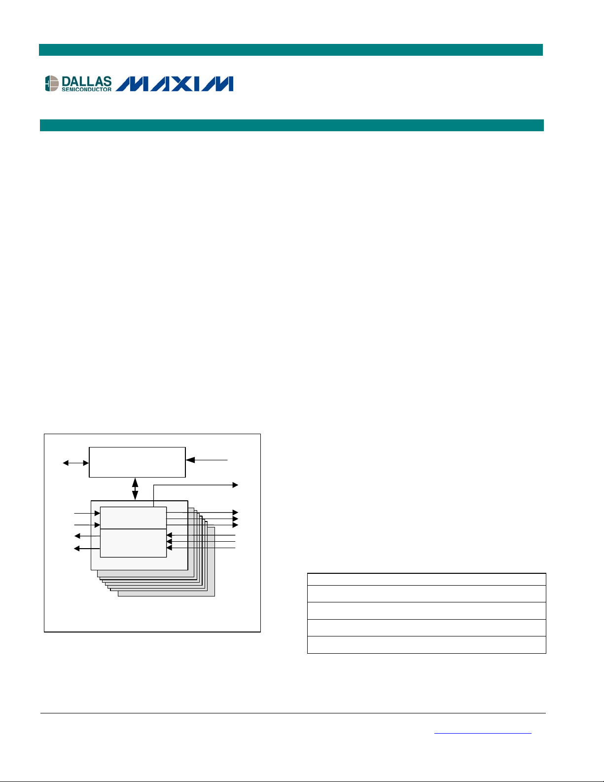
FUNCTIONAL DIAGRAM
Jtag
RTIP
RRING
TTTIP
TRING
Software Control,
Hardware Control
and JTAG
Receiver
Transmitter
MODESEL
RLOS
RPOS
RNEG
RCLK
TPOS
TNEG
TCLK
FEATURES
8 Complete E1, T1, or J1 Short-Haul Line
Interface Units
Independent E1, T1, or J1 Selections
Internal Software-Selectable Transmit and
Receive-Side Termination
Crystal-Less Jitter Attenuator
Selectable Single-Rail and Dual-Rail Mode
and AMI or HDB3/B8ZS Line Encoding and
Decoding
Detection and Generation of AIS
Digital/Analog Loss-of-Signal Detection as
per T1.231, G.775, and ETS 300 233
External Master Clock can be Multiple of
2.048MHz or 1.544MHz for T1/J1 or E1
Operation; This Clock will be Internally
Adapted for T1 or E1 Use
Built-In BERT Tester for Diagnostics
8-Bit Parallel Interface Support for Intel or
Motorola Mode or a 4-Wire Serial Interface
Hardware Mode Interface Support
Transmit Short-Circuit Protection
G.772 Nonintrusive Monitoring
Specification Compliance to the Latest T1
and E1 Standards—ANSI T1.102, AT&T Pub
62411, T1.231, T1.403, ITU-T G.703, G.742,
G.775, G.823, ETS 300 166, and ETS 300 233
Single 3.3V Supply with 5V Tolerant I/O
JTAG Boundary Scan as per IEEE 1149.1
144-Pin eLQFP Package
1
8
DS26303
Note: Some revisions of this device may incorporate deviations from published specifications known as errata. Multiple revisions of any device
may be simultaneously available through various sales channels. For information about device errata, click here: www.maxim-ic.com/errata
ORDERING INFORMATION
PART
DS26303L-XXX 0°C to +70°C 144 eLQFP
DS26303L-XXX+ 0°C to +70°C 144 eLQFP
DS26303LN-XXX -40°C to +85°C 144 eLQFP
DS26303LN-XXX+ -40°C to +85°C 144 eLQFP
Note: When XXX is 075, the part defaults to 75Ω impedance in E1
mode; when XXX is 120, the part defaults to 120
+ Denotes a lead-free/RoHS-compliant package.
e = Exposed Pad.
TEMP RANGE PIN-PACKAGE
Ω
impedance.
1 of 101 REV: 053107
.
Page 2

DS26303: 3.3V, T1/E1/J1, Short-Haul, Octal Line Interface Unit
TABLE OF CONTENTS
1 DETAILED DESCRIPTION...............................................................................................................6
2 TELECOM SPECIFICATIONS COMPLIANCE.................................................................................7
3 BLOCK DIAGRAMS.........................................................................................................................9
4 PIN DESCRIPTION.........................................................................................................................11
4.1 HARDWARE AND HOST PORT OPERATION ......................................................................................20
4.1.1 Hardware Mode................................................................................................................................... 20
4.1.2 Serial Port Operation .......................................................................................................................... 21
4.1.3 Parallel Port Operation........................................................................................................................ 22
4.1.4 Interrupt Handling ............................................................................................................................... 22
5 REGISTERS....................................................................................................................................24
5.1 REGISTER DESCRIPTION ...............................................................................................................29
5.1.1 Primary Registers................................................................................................................................ 29
5.1.2 Secondary Registers........................................................................................................................... 38
5.1.3 Individual LIU Registers...................................................................................................................... 40
5.1.4 BERT Registers ..................................................................................................................................47
6 FUNCTIONAL DESCRIPTION........................................................................................................54
6.1 POWER-UP AND RESET ................................................................................................................. 54
6.2 MASTER CLOCK ............................................................................................................................54
6.3 TRANSMITTER ...............................................................................................................................55
6.3.1 Transmit Line Templates .................................................................................................................... 56
6.3.2 LIU Transmit Front-End ...................................................................................................................... 58
6.3.3 Dual-Rail Mode ................................................................................................................................... 59
6.3.4 Single-Rail Mode................................................................................................................................. 59
6.3.5 Zero Suppression—B8ZS or HDB3 .................................................................................................... 59
6.3.6 Transmit Power-Down ........................................................................................................................ 59
6.3.7 Transmit All Ones................................................................................................................................ 59
6.3.8 Driver Fail Monitor............................................................................................................................... 59
6.4 RECEIVER .....................................................................................................................................59
6.4.1 Peak Detector and Slicer ....................................................................................................................59
6.4.2 Clock and Data Recovery ...................................................................................................................59
6.4.3 Loss of Signal...................................................................................................................................... 60
6.4.4 AIS ...................................................................................................................................................... 60
6.4.5 Bipolar Violation and Excessive Zero Detector................................................................................... 62
6.4.6 LIU Receiver Front-End ......................................................................................................................62
6.5 HITLESS-PROTECTION SWITCHING (HPS) ......................................................................................62
6.6 JITTER ATTENUATOR .....................................................................................................................64
6.7 G.772 MONITOR ...........................................................................................................................65
6.8 LOOPBACKS ..................................................................................................................................65
6.8.1 Analog Loopback ................................................................................................................................65
6.8.2 Digital Loopback.................................................................................................................................. 65
6.8.3 Remote Loopback............................................................................................................................... 66
6.8.4 Dual Loopback .................................................................................................................................... 67
6.9 BERT...........................................................................................................................................68
6.9.1 Configuration and Monitoring.............................................................................................................. 68
6.9.2 BERT Interrupt Handling..................................................................................................................... 69
6.9.3 Receive Pattern Detection ..................................................................................................................69
6.9.4 Transmit Pattern Generation............................................................................................................... 71
7 JTAG BOUNDARY SCAN ARCHITECTURE AND TEST ACCESS PORT...................................72
7.1 TAP CONTROLLER STATE MACHINE ..............................................................................................73
7.1.1 Test-Logic-Reset................................................................................................................................. 73
7.1.2 Run-Test-Idle ...................................................................................................................................... 73
7.1.3 Select-DR-Scan .................................................................................................................................. 73
7.1.4 Capture-DR......................................................................................................................................... 73
2 of 101
Page 3

DS26303: 3.3V, T1/E1/J1, Short-Haul, Octal Line Interface Unit
7.1.5 Shift-DR...............................................................................................................................................73
7.1.6 Exit1-DR.............................................................................................................................................. 73
7.1.7 Pause-DR............................................................................................................................................ 73
7.1.8 Exit2-DR.............................................................................................................................................. 73
7.1.9 Update-DR ..........................................................................................................................................73
7.1.10 Select-IR-Scan.................................................................................................................................... 74
7.1.11 Capture-IR........................................................................................................................................... 74
7.1.12 Shift-IR................................................................................................................................................ 74
7.1.13 Exit1-IR ...............................................................................................................................................74
7.1.14 Pause-IR............................................................................................................................................. 74
7.1.15 Exit2-IR ...............................................................................................................................................74
7.1.16 Update-IR............................................................................................................................................ 74
7.2 INSTRUCTION REGISTER................................................................................................................76
7.2.1 EXTEST ..............................................................................................................................................76
7.2.2 HIGHZ................................................................................................................................................. 76
7.2.3 CLAMP................................................................................................................................................ 76
7.2.4 SAMPLE/PRELOAD ...........................................................................................................................76
7.2.5 IDCODE ..............................................................................................................................................76
7.2.6 BYPASS.............................................................................................................................................. 76
7.3 TEST REGISTERS ..........................................................................................................................77
7.3.1 Boundary Scan Register..................................................................................................................... 77
7.3.2 Bypass Register.................................................................................................................................. 77
7.3.3 Identification Register ......................................................................................................................... 77
8 OPERATING PARAMETERS.........................................................................................................78
9 THERMAL CHARACTERISTICS....................................................................................................79
10 AC CHARACTERISTICS................................................................................................................80
10.1 LINE INTERFACE CHARACTERISTICS ...............................................................................................80
10.2 PARALLEL HOST INTERFACE TIMING CHARACTERISTICS .................................................................81
10.3 SERIAL PORT ................................................................................................................................93
10.4 SYSTEM TIMING ............................................................................................................................94
10.5 JTAG TIMING................................................................................................................................96
11 PIN CONFIGURATION ...................................................................................................................97
11.1 144-PIN LQFP WITH EXPOSED PAD ..............................................................................................97
12 PACKAGE INFORMATION ............................................................................................................98
12.1 144-PIN LQFP WITH EXPOSED PAD PACKAGE OUTLINE (56-G6037-002) (SHEET 1 OF 2) .............. 98
12.2 144-PIN LQFP WITH EXPOSED PAD PACKAGE OUTLINE (SHEET 2 OF 2)......................................... 99
13 DOCUMENT REVISION HISTORY...............................................................................................100
3 of 101
Page 4

DS26303: 3.3V, T1/E1/J1, Short-Haul, Octal Line Interface Unit
LIST OF FIGURES
Figure 3-1. Block Diagram ........................................................................................................................................... 9
Figure 3-2. Receive Logic Detail................................................................................................................................ 10
Figure 3-3. Transmit Logic Detail............................................................................................................................... 10
Figure 4-1. 144-Pin eLQFP Pin Assignment ............................................................................................................. 19
Figure 4-2. Serial Port Operation for Write Access ................................................................................................... 21
Figure 4-3. Serial Port Operation for Read Access with CLKE = 0 ........................................................................... 21
Figure 4-4. Serial Port Operation for Read Access with CLKE = 1 ........................................................................... 22
Figure 4-5. Interrupt Handling Flow Diagram ............................................................................................................ 23
Figure 6-1. Prescaler PLL and Clock Generator ....................................................................................................... 54
Figure 6-2. T1 Transmit Pulse Templates ................................................................................................................. 56
Figure 6-3. E1 Transmit Pulse Templates ................................................................................................................. 57
Figure 6-4. LIU Front-End.......................................................................................................................................... 58
Figure 6-5. HPS Logic ............................................................................................................................................... 63
Figure 6-6. HPS Block Diagram................................................................................................................................. 63
Figure 6-7. Jitter Attenuation ..................................................................................................................................... 64
Figure 6-8. Analog Loopback..................................................................................................................................... 65
Figure 6-9. Digital Loopback...................................................................................................................................... 66
Figure 6-10. Remote Loopback ................................................................................................................................. 66
Figure 6-11. Dual Loopback ...................................................................................................................................... 67
Figure 6-12. PRBS Synchronization State Diagram.................................................................................................. 70
Figure 6-13. Repetitive Pattern Synchronization State Diagram............................................................................... 71
Figure 7-1. JTAG Functional Block Diagram ............................................................................................................. 72
Figure 7-2. TAP Controller State Diagram................................................................................................................. 75
Figure 10-1. Intel Nonmuxed Read Cycle ................................................................................................................. 82
Figure 10-2. Intel Mux Read Cycle ............................................................................................................................ 83
Figure 10-3. Intel Nonmux Write Cycle...................................................................................................................... 85
Figure 10-4. Intel Mux Write Cycle ............................................................................................................................ 86
Figure 10-5. Motorola Nonmux Read Cycle .............................................................................................................. 88
Figure 10-6. Motorola Mux Read Cycle..................................................................................................................... 89
Figure 10-7. Motorola Nonmux Write Cycle .............................................................................................................. 91
Figure 10-8. Motorola Mux Write Cycle ..................................................................................................................... 92
Figure 10-9. Serial Bus Timing Write Operation........................................................................................................ 93
Figure 10-10. Serial Bus Timing Read Operation with CLKE = 0.............................................................................. 93
Figure 10-11. Serial Bus Timing Read Operation with CLKE = 1.............................................................................. 93
Figure 10-12. Transmitter Systems Timing ............................................................................................................... 94
Figure 10-13. Receiver Systems Timing ................................................................................................................... 95
Figure 10-14. JTAG Timing ....................................................................................................................................... 96
4 of 101
Page 5

DS26303: 3.3V, T1/E1/J1, Short-Haul, Octal Line Interface Unit
LIST OF TABLES
Table 2-1. T1-Related Telecommunications Specifications ........................................................................................ 7
Table 2-2. E1-Related Telecommunications Specifications ........................................................................................ 8
Table 4-1. Pin Descriptions........................................................................................................................................ 11
Table 4-2. Hardware Mode Configuration Examples................................................................................................. 20
Table 4-3. Parallel Port Mode Selection and Pin Functions ...................................................................................... 22
Table 5-1. Primary Register Set ................................................................................................................................ 24
Table 5-2. Secondary Register Set............................................................................................................................ 25
Table 5-3. Individual LIU Register Set....................................................................................................................... 25
Table 5-4. BERT Register Set ................................................................................................................................... 26
Table 5-5. Primary Register Set Bit Map ................................................................................................................... 27
Table 5-6. Secondary Register Set Bit Map .............................................................................................................. 27
Table 5-7. Individual LIU Register Set Bit Map.......................................................................................................... 28
Table 5-8. BERT Register Bit Map ............................................................................................................................ 28
Table 5-9. G.772 Monitoring Control ......................................................................................................................... 32
Table 5-10. TST Template Select Transceiver Register ........................................................................................... 35
Table 5-11. Template Selection................................................................................................................................. 35
Table 5-12. Address Pointer for Bank Selection........................................................................................................ 37
Table 5-13. MCLK Selections .................................................................................................................................... 42
Table 5-14. Jitter Attenuator Bandwidth Selections................................................................................................... 43
Table 5-15. PLL Clock Select .................................................................................................................................... 45
Table 5-16. Clock A Select ........................................................................................................................................ 45
Table 6-1. Telecommunications Specification Compliance for DS26303 Transmitters ............................................ 55
Table 6-2. Registers Related to Control of DS26303 Transmitters ........................................................................... 55
Table 6-3. DS26303 Template Selections................................................................................................................. 56
Table 6-4. LIU Front-End Values............................................................................................................................... 58
Table 6-5. Loss Criteria T1.231, G.775, and ETS 300 233 Specifications................................................................ 60
Table 6-6. AIS Criteria T1.231, G.775, and ETS 300 233 Specifications.................................................................. 61
Table 6-7. AIS Detection and Reset Criteria ............................................................................................................. 61
Table 6-8. Registers Related to AIS Detection.......................................................................................................... 61
Table 6-9. BPV, Code Violation, and Excessive Zero Error Reporting ..................................................................... 62
Table 6-10. Pseudorandom Pattern Generation........................................................................................................ 68
Table 6-11. Repetitive Pattern Generation ................................................................................................................ 68
Table 7-1. Instruction Codes for IEEE 1149.1 Architecture....................................................................................... 76
Table 7-2. ID Code Structure..................................................................................................................................... 77
Table 7-3 Device ID Codes........................................................................................................................................ 77
Table 8-1. Recommended DC Operating Conditions................................................................................................ 78
Table 8-2. Capacitance.............................................................................................................................................. 78
Table 8-3. DC Characteristics.................................................................................................................................... 78
Table 9-1. Thermal Characteristics............................................................................................................................ 79
Table 10-1. Transmitter Characteristics..................................................................................................................... 80
Table 10-2. Receiver Characteristics......................................................................................................................... 80
Table 10-3. Intel Read Mode Characteristics ............................................................................................................ 81
Table 10-4. Intel Write Cycle Characteristics ............................................................................................................ 84
Table 10-5. Motorola Read Cycle Characteristics ..................................................................................................... 87
Table 10-6. Motorola Write Cycle Characteristics ..................................................................................................... 90
Table 10-7. Serial Port Timing Characteristics .......................................................................................................... 93
Table 10-8. Transmitter System Timing .................................................................................................................... 94
Table 10-9. Receiver System Timing......................................................................................................................... 95
Table 10-10. JTAG Timing Characteristics................................................................................................................ 96
5 of 101
Page 6

DS26303: 3.3V, T1/E1/J1, Short-Haul, Octal Line Interface Unit
1 DETAILED DESCRIPTION
The DS26303 is a single-chip, 8-channel, short-haul line interface unit (LIU) for T1 (1.544Mbps) and E1
(2.048Mbps) applications. Eight independent receivers and transmitters are provided in an eLQFP package. The
LIUs can be individually selected for T1, J1, or E1 operation. The LIU requires a single reference clock called
MCLK. MCLK can be either 1.544MHz or 2.048MHz or a multiple thereof, and either frequency can be internally
adapted for T1, J1, or E1 mode. Internal impedance match provided for both transmit and receive paths reduces
external component count. The transmit waveforms are compliant to G.703 and T1.102 specifications. The
DS26303 provides software-selectable internal transmit termination for 100Ω T1 twisted pair, 110Ω J1 twisted pair,
120Ω E1 twisted pair, and 75Ω E1 coaxial applications. The transmitters have fast high-impedance capability and
can be individually powered down.
The receivers can function with up to 15dB of receive signal attenuation for T1 mode and E1 mode. The DS26303
can be configured as a 7-channel LIU with channel 1 used for nonintrusive monitoring in accordance with G.772.
The receivers and transmitters can be programmed into single-rail or dual-rail mode. AMI or HDB/B8ZS encoding
and decoding is selectable in single-rail mode. A 128-bit crystal-less on-board jitter attenuator for each LIU can be
placed in the receive or transmit directions. The jitter attenuator meets the ETS CTR12/13 ITU-T G.736, G.742,
G.823, and AT&T Pub 62411 specifications.
The DS26303 detects and generates AIS in accordance with T1.231, G.775, and ETS 300 233. Loss of signal is
detected in accordance with T1.231, G.775, and ETS 300 233. The DS26303 can perform digital, analog, remote,
and dual loopbacks on individual LIUs. JTAG boundary scan is provided for the digital pins.
The DS26303 can be configured using an 8-bit multiplexed or nonmultiplexed Intel or Motorola port, a 4-pin serial
port, or in limited modes of operation using hardware mode.
The analog AMI/HDB3 waveform of the E1 line or the AMI/B8ZS waveform of the T1 line is transformer coupled
into the RTIP and RRING pins of the DS26303. The user has the option to select internal termination of 75Ω,
100Ω, 110Ω, or 120Ω applications. The device recovers clock and data from the analog signal and passes it
through a selectable jitter attenuator, outputting the received line clock at RCLK and data at RPOS and RNEG.
The DS26303 receivers can recover data and clock for up to 15dB of attenuation of the transmitted signals in T1
and E1 mode. Receiver 1 can monitor the performance of receivers 2 to 8 or transmitters 2 to 8.
The DS26303 contains eight identical transmitters. Digital transmit data is input at TPOS/TNEG with reference to
TCLK. The data at these pins can be single-rail or dual-rail. This data is processed by waveshaping circuitry and
line drivers to output a pulse at TTIP and TRING in accordance with ANSI T1.102 for T1/J1 or G.703 for E1 mask.
The DS26303 drives the E1 or T1 line from the TTIP and TRING pins through a coupling transformer. The
DS26303 requires a 1:2 transformer for the transmit path and a 2:1 transformer for the receive path.
6 of 101
Page 7

DS26303: 3.3V, T1/E1/J1, Short-Haul, Octal Line Interface Unit
2 TELECOM SPECIFICATIONS COMPLIANCE
The DS26303 LIU meets all the relevant latest telecommunications specifications. Table 2-1 provides the T1
specifications and
Table 2-1. T1-Related Telecommunications Specifications
ANSI T1.102–Digital Hierarchy Electrical Interface
AMI Coding
B8ZS Substitution Definition
DS1 Electrical Interface. Line rate ±32ppm; Pulse Amplitude between 2.4V to 3.6 V peak; Power level between
12.6dBm to 17.9dBm. The T1 pulse mask is provided that we comply. DSX-1 for cross connects the return loss is
greater than 26dB. The DSX-1 cable is restricted up to 655 feet.
This specification also provides cable characteristics of DSX-Cross Connect cable—22 AVG cable of 1000 feet.
ANSI T1.231–Digital Hierarchy–Layer 1 in Service Performance Monitoring
BPV Error Definition, Excessive Zero Definition, LOS description, AIS definition
ANSI T1.403–Network and Customer Installation Interface–DS1 Electrical Interface
Description of the Measurement of the T1 Characteristics—100Ω, pulse shape and template according to T1.102;
power level 12.4dBm to 19.7dBm when all ones are transmitted.
LBO for the Customer Interface (CI) is specified as 0dB, 7.5dB, and 15dB. Line rate is ±32ppm.
Pulse Amplitude is 2.4V to 3.6V.
AIS generation as unframed all ones is defined.
The total cable attenuation is defined as 22dB. The DS26303 functions up to 36dB cable loss.
Note that the pulse mask defined by T1.403 and T1.102 are different—specifically at Times 0.61, -0.27, -34,
and 0.77. The DS26303 is compliant to both templates.
Pub 62411
This specification has tighter jitter tolerance and transfer characteristics than other specifications. The jitter transfer
characteristics are tighter than G.736 and jitter tolerance is tighter the G.823.
Table 2-2 provides the E1 specifications for the relevant sections applicable to the DS26303.
7 of 101
Page 8

DS26303: 3.3V, T1/E1/J1, Short-Haul, Octal Line Interface Unit
Table 2-2. E1-Related Telecommunications Specifications
ITU-T G.703 Physical/Electrical Characteristics of G.703 Hierarchical Digital Interfaces
Defines the 2048kbps bit rate: 2048 ±50ppm. The transmission media are 75Ω coax or 120Ω twisted pair; peak-topeak space voltage is ±0.237V; nominal pulse width is 244ns.
Return loss: 51Hz to 102Hz is 6dB, 102Hz to 3072Hz is 8dB, 2048Hz to 3072Hz is 14dB
Nominal peak voltage is 2.37V for coax and 3V for twisted pair.
The pulse mask for E1 is defined in G.703.
Defines the 2048 kHz synchronization interface (Chapter 13). Contact factory for usage details.
ITU-T G.736 Characteristics of Synchronous Digital Multiplex Equipment Operating at 2048kbps
The peak-to-peak jitter at 2048kbps must be less than 0.05UI at 20Hz to 100Hz.
Jitter transfer between 2.048 synchronization signal and 2.048 transmission signal is provided.
ITU-T G.742 Second-Order Digital Multiplex Equipment Operating at 8448kbps
The DS26303 jitter attenuator is compliant with jitter transfer curve for sinusoidal jitter input.
ITU-T G.772
This specification provides the method for using receiver for transceiver 0 as a monitor for the rest of the seven
transmitter/receiver combinations.
ITU-T G.775
An LOS detection criterion is defined.
ITU-T G.823–The control of jitter and wander within digital networks that are based on 2.048kbps Hierarchy
G.823 provides the jitter amplitude tolerance at different frequencies, specifically 20Hz, 2.4kHz, 18kHz, and
100kHz.
ETS 300 166
This specification provides transmit return loss of 6dB for a range of 0.25fb to 0.05fb, and 8dB for a range of 0.05fb
to 1.5fb where fb equals 2.048kHz for 2.048kbps interface.
ETS 300 233
This specification provides LOS and AIS signal criteria for E1 mode.
Pub 62411
This specification has tighter jitter tolerance and transfer characteristics than other specifications. The jitter transfer
characteristics are tighter than G.736 and jitter tolerance is tighter than G.823.
8 of 101
Page 9
3 BLOCK DIAGRAMS
Figure 3-1. Block Diagram
DS26303: 3.3V, T1/E1/J1, Short-Haul, Octal Line Interface Unit
RRING
RTIP
TRING
TTIP
OE
TYPICAL OF ALL 8 CHANNELS
Optional
Termination
Analog Loopback
Filter
Line Drivers
Peak Detector
Unframed All
Ones Insertion
VCO/PLL
Clock/Data
Wave Shaping
Recovery
Jitter Attenuator
Remote Loopback (Dual Mode)
MUX
Local Loopback
Jitter Attenuator
T1CLK E1CLK
MUX
2.048MHz to
1.544MHz PLL
Remote Loopback
Receive Logic
DS26303
Transmit Logic
RLOS
RPOS/RDAT
RCLK
RNEG/CV
TPOS/TDAT
TCLK
TNEG
Reset
Reset
Port Interface
85
MUX
CLKE
WRB/DSB/SDI
RDB/RWB
MOTEL
RDY/ACKB/SDO
ASB/ALE/SCLK
BSWB
D7/AD7/
A0 to A4
D0 to D6/
AD0 to AD6
Control
Interrupt
CSB
and
INTB
MODESEL
JTAG PORT
JTMS
JTRSTB
JTCLK
JTDI
JTDO
T1CLK E1CLK
88
Master Clock
Adapter
MCLK
9 of 101
Page 10
Figure 3-2. Receive Logic Detail
DS26303: 3.3V, T1/E1/J1, Short-Haul, Octal Line Interface Unit
RCLK
POS
NEG
EZDE
Excessive
Zero
Detect
T1.231
Decoder (G.703, T1.102)
BPVs, Code Violatiions
B8ZS/HDB3/AMI
(T1.231, O.161)
ENCODE
LCS
CODE
Figure 3-3. Transmit Logic Detail
LOS
RCLK
IAISEL
AISEL
EN
Insert
(AIS)
RPOS
RNEG/CV
MCLK
NRZ Data
BPV/CV/EXZ
ENCV
CVDEB
ENCODE
AIS
Detector
G.775, ETSI 300233,
T1.231
LASCS
MUX
All Ones
SRMS
To Remote
Loopback
BEIR
BPV
Insert
SRMS
MUX
LCS
CODE
ENCODE
B8ZS/HDB3/AMI
Coder (G.703,
T1.102)
TPOS/
TDATA
TNEG/
BPV
TCLK
10 of 101
Page 11
DS26303: 3.3V, T1/E1/J1, Short-Haul, Octal Line Interface Unit
4 PIN DESCRIPTION
Table 4-1. Pin Descriptions
NAME PIN TYPE FUNCTION
ANALOG TRANSMIT AND RECEIVE
TTIP1 45
TTIP2 52
TTIP3 57
TTIP4 64
TTIP5 117
TTIP6 124
TTIP7 129
TTIP8 136
TRING1 46
TRING2 51
TRING3 58
TRING4 63
TRING5 118
TRING6 123
TRING7 130
TRING8 135
RTIP1 48
RTIP2 55
RTIP3 60
RTIP4 67
RTIP5 120
RTIP6 127
RTIP7 132
RTIP8 139
RRING1 49
RRING2 54
RRING3 61
RRING4 66
RRING5 121
RRING6 126
RRING7 133
RRING8 138
Analog
Output
Analog
Output
Analog
Input
Analog
Input
Transmit Bipolar Tip for Channel 1 to 8. These pins are
differential line-driver tip outputs. These pins will be high
impedance if pin OE is low or the corresponding
high. If the corresponding clock TCLKn is low for 64 MCLKs, the
corresponding transmitter is put in power-down mode. The
differential outputs of TTIPn and TRINGn can provide internal
matched impedance for E1 75Ω, E1 120Ω, T1 100Ω, or J1 110Ω.
Transmit Bipolar Ring for Channel 1 to 8. These pins are
differential line-driver ring outputs. These pins will be high
impedance if pin OE is low or the corresponding
high. If the corresponding clock TCLKn is low for 64 MCLKs, the
corresponding transmitter is put in power-down mode. The
differential outputs of TTIPn and TRINGn can provide internal
matched impedance for E1 75Ω, E1 120Ω, T1 100Ω, or J1 110Ω.
Receive Bipolar Tip for Channel 1 to 8. Receive analog input for
differential receiver. Data and clock are recovered and output at
RPOSn/RNEGn and RCLKn pins, respectively. The differential
inputs of RTIPn and RRINGn can provide internal matched
impedance for E1 75Ω, E1 120Ω, T1 100Ω, or J1 110Ω.
Receive Bipolar Ring for Channel 1 to 8. Receive analog input
for differential receiver. Data and clock are recovered and output
at RPOSn/RNEGn and RCLKn pins, respectively. The differential
inputs of RTIPn and RRINGn can provide internal matched
impedance for E1 75Ω, E1 120Ω, T1 100Ω, or J1 110Ω.
OEB.OEBn bit is
OEB.OEBn bit is
11 of 101
Page 12

DS26303: 3.3V, T1/E1/J1, Short-Haul, Octal Line Interface Unit
NAME PIN TYPE FUNCTION
DIGITAL Tx/Rx
TPOS1/TDATA1 37
TPOS2/TDATA2 30
TPOS3/TDATA3 80
TPOS4/TDATA4 73
I
TPOS5/TDATA5 108
TPOS6/TDATA6 101
TPOS7/TDATA7 8
TPOS8/TDATA8 1
Transmit Positive-Data Input for Channel 1 to 8/Transmit Data
Input for Channel 1 to 8
TPOS[1:8]: When the DS26303 is configured in dual-rail mode, the
data input to TPOSn is output as a positive pulse on the line
(TTIPn and TRINGn) as follows:
TPOSn TNEGn Output Pulse
0 0 Space
0 1 Negative Pulse
1 0 Positive Pulse
1 1 Space
TDATA[1:8]: When the device is configured in single-rail mode,
NRZ data is input to TDATAn. The data is HDB3, B8ZS or AMI
encoded before being output to the line.
TNEG1 38
TNEG2 31
Transmit Negative Data for Channel 1 to 8. When the DS26303
is configured in dual-rail mode, the data input to TNEGn is output
TNEG3 79
TNEG4 72
I
TNEG5 109
TNEG6 102
as a negative pulse on the line (TTIPn and TRINGn) as follows:
TPOSn TNEGn Output Pulse
0 0 Space
0 1 Negative Pulse
1 0 Positive Pulse
TNEG7 7
1 1 Space
TNEG8 144
TCLK1 36
TCLK2 29
Transmit Clock for Channel 1 to 8. The transmit clock must be
1.544MHz for T1 or 2.048MHz for E1 mode. TCLKn is the clock
used to sample the data on TPOSn/TNEGn or TDATn on the
falling edge. TCLKn can be inverted.
TCLK3 81
If TCLKn is high for 16 or more MCLKs, then an all-ones signal is
TCLK4 74
TCLK5 107
TCLK6 100
TCLK7 9
TCLK8 2
RPOS1/RDATA1 40
RPOS2/RDATA2 33
RPOS3/RDATA3 77
RPOS4/RDATA4 70
RPOS5/RDATA5 111
RPOS6/RDATA6 104
RPOS7/RDATA7 5
RPOS8/RDATA8 142
I
O,
tri-state
transmitted on the corresponding line (TTIPn and TRINGn). When
TCLKn starts clocking again, normal operation will resume on the
corresponding line.
If TCLKn is low for 64 or more MCLKs, the corresponding
transmitter channel will power down and the line will be put into
high impedance. When TCLKn starts clocking again the
corresponding transmitter will power up, resume normal operation,
and the line will come out of high impedance.
Receive Positive-Data Output for Channel 1 to 8/Receive Data
Output for Channel 1 to 8
RPOS[1:8]: In dual-rail mode, this output indicates a positive pulse
on RTIPn/RRINGn. If a given receiver is in power-down mode, the
corresponding RPOSn pin is high impedance.
RDATA[1:8]: In single-rail mode, NRZ data is output to this pin.
Note: During an RLOS condition, the RPOSn/RDATAn output
remainactive.
12 of 101
Page 13
DS26303: 3.3V, T1/E1/J1, Short-Haul, Octal Line Interface Unit
NAME PIN TYPE FUNCTION
RNEG1/CV1 41
Receive Negative-Data Output for Channel 1 to 8/Code
Violation for Channel 1 to 8
RNEG2/CV2 34
RNEG[1:8]: In dual-rail mode, this output indicates a negative
RNEG3/CV3 76
RNEG4/CV4 69
RNEG5/CV5 112
tri-state
RNEG6/CV6 105
O,
pulse on RTIPn/RRINGn. If a given receiver is in power-down
mode, the corresponding RNEGn pin is high impedance.
CV[1:8]: In single-rail mode, bipolar violation, code violation, and
excessive zeros are reported by driving CVn high for one clock
cycle. If HDB3 or B8ZS encoding is not selected, this pin indicates
only BPVs.
RNEG7/CV7 4
Note: During an RLOS condition, the RNEGn/CVn output remains
RNEG8/CV8 141
active.
RCLK1 39
RCLK2 32
RCLK3 78
RCLK4 71
RCLK5 110
O,
tri-state
RCLK6 103
Receive Clock for Channel 1 to 8. The receive data
RPOSn/RNEGn or RDATn is clocked out on the rising edge of
RCLKn. RCLKn can be inverted. If a given receiver is in powerdown mode, RCLKn is high impedance.
RCLK7 6
RCLK8 143
Master Clock. This is an independent free-running clock that can
be a multiple of 2.048MHz ±50ppm for E1 mode or 1.544MHz
±50ppm for T1 mode. The clock selection is available by
MCLK 10 I
MPS0, MPS1, FREQS, and PLLE. A multiple of 2.048MHz can be
internally adapted to 1.544MHz and a multiple of 1.544MHz can
be internally adapted to 2.048MHz. In hardware mode, internal
adaptation is not available so the user must provide 2.048MHz
±50ppm for E1 mode or 1.544MHz ±50ppm for T1 mode.
Loss-of-Signal Output/T1-E1 Clock
MC bits
RLOS1: This output goes high when there are no transitions on
the receiveline over a specified interval. The output goes low when
there is sufficient ones density on the receiveline. The RLOS
assertion and desertion criteria are described in the Functional
RLOS1/TECLK 42 O
Description section. The RLOS outputs can be configured to
comply with T1.231, ITU-T G.775, or ETS 300 233. In hardware
mode, ETS 300 233 “RLOS Criteria” is not available.
TECLK: When enabled (
a T1- or E1-programmable clock output. For T1 or E1 frequency
selection, see the
hardware mode.
RLOS2 35
RLOS3 75
RLOS4 68
RLOS5 113
O
Loss-of-Signal Output
RLOS[2:8]: RLOS2: This output goes high when there are no
transitions on the receiveline over a specified interval. The output
goes low when there is sufficient ones density on the receiveline.
The RLOS assertion and desertion criteria are described in the
RLOS6 106
Functional Description (Section
configured to comply with T1.231, ITU-T G.775, or ETS 300 233.
RLOS7 3
In hardware mode, ETS 300 233 “RLOS Criteria” is not available.
RLOS8 140
MC.TECLKE is set), this output becomes
CCR register. This option is not available in
6). The RLOS outputs can be
13 of 101
Page 14

DS26303: 3.3V, T1/E1/J1, Short-Haul, Octal Line Interface Unit
NAME PIN TYPE FUNCTION
Clock A. This output becomes a programmable clock output when
CLKA 93
O,
tri-state
enabled (
register. This option is not available in hardware mode. If this
MC.CLKAE is set). For frequency options, see the CCR
option is not used, the pin should be left unconnected.
I
N.C. 94
(pulled
to V
No Connection. Pin should be left unconnected or grounded.
)
SS
HARDWARE AND PORT OPERATION
Mode Selection. This pin is used to select the control mode of the
DS26303.
MODESEL 11
MUX/
TIMPRM
MOTEL/
CODE
43 I
88 I
(pulled
V
DDIO
I
to
Low → Hardware Mode
/2 → Serial Host Mode
V
DDIO
High → Parallel Host Mode
/2)
Note: When left unconnected, do not route signals with fast
transitions near MODESEL. This practice minimizes capacitive
coupling.
Multiplexed/Nonmultiplexed Select Pin/
Transmit Impedance/Receive Impedance Match
MUX: In host mode with a parallel port, this pin is used to select
multiplexed address and data operation or separate address and
data. When mux is a high, multiplexed address and data is used.
TIMPRM: In hardware mode, this pin selects the internal transmit
termination impedance and receive impedance match for E1 mode
and T1/J1 mode.
0 → 75Ω for E1 mode or 100Ω for T1 mode
1 → 120Ω for E1 mode or 110Ω for J1 mode
Note: If the part number ends with 120, the default is 120
low and 75
Motorola Intel Select/Code
Ω
when high for El mode only.
MOTEL: When in parallel host mode, this pin selects Motorola
mode when low and Intel mode when high.
CODE: In hardware mode, AMI encoding/decoding for all the LIUs
is selected when the pin is high. When the pin is low, B8ZS is
selected for T1 mode and HDB3 for E1 mode for all the LIUs.
Chip Select Bar/Jitter Attenuator Select
Ω
when
CSB/
JAS
87
I
(In HW
mode,
pulled
to
/2)
V
DDIO
CSB: This signal must be low during all accesses to the registers.
JAS: In hardware mode, this pin is used as a jitter attenuator
select.
Low → Jitter attenuator is in the transmit path.
/2 → Jitter attenuator is not used.
V
DDIO
High → Jitter attenuator is in the receive path.
Note: When left unconnected in hardware mode, do not route
signals with fast transitions near JAS, in order to minimize
capacitive coupling.
14 of 101
Page 15

DS26303: 3.3V, T1/E1/J1, Short-Haul, Octal Line Interface Unit
NAME PIN TYPE FUNCTION
Serial Clock/Address Latch Enable/Address Strobe
Bar/Template Selection 2
SCLK: In the serial host mode, this pin is the serial clock. Data on
SDI is clocked on the rising edge of SCLK. The data is clocked on
SDO on the rising edge of SCLK if CLKE is high. If CLKE is low
the data on SDO is clocked on the falling edge of SCLK.
SCLK/ALE/
ASB/TS2
86 I
ALE: In parallel Intel multiplexed mode, the address lines are
latched on the falling edge of ALE. Tie ALE pin high if using
nonmultiplexed mode.
ASB: In parallel Motorola multiplexed mode, the address is
sampled on the falling edge of ASB. Tie ASB pin high if using
nonmultiplexed mode.
TS2: In hardware mode, this pin signal is one of the template
selection bits. See
Read Bar/Read Write Bar/Template Selection 1
RDB: In Intel host mode, this pin must be low for read operation.
RDB/RWB/TS1 85 I
RWB: In Motorola mode, this pin is low for write operation and
high for read operation.
TS1: In hardware mode, this pin signal is one of the template
selection bits. See
Serial Data Input/Write Bar/Data Strobe Bar/Template
Selection 0
SDI: In the serial host mode, this pin is the serial input SDI. It is
sampled on the rising edge of SCLK. Data is input LSB first.
WRB: In Intel host mode, this pin is active low during write
operation. The data is sampled on the rising edge of WRB.
SDI/WRB/DSB/TS0 84 I
DSB: In the parallel Motorola mode, this pin is active low. During a
write operation the data is sampled on the rising edge of DSB.
During a read operation the data (D[7:0] or AD[7:0]) is driven on
the falling edge of DSB. In the nonmultiplexed Motorola mode, the
address bus (A[5:0]) is latched on the falling edge of DSB.
Table 5-11.
Table 5-11.
TS0: In hardware mode, this pin signal is one of the template
select bits. See
Table 5-11.
15 of 101
Page 16

DS26303: 3.3V, T1/E1/J1, Short-Haul, Octal Line Interface Unit
NAME PIN TYPE FUNCTION
Serial Data Out/Ready Output/Acknowledge Bar/Receive
Impedance Off
SDO: In serial host mode, the SDO data is output on this pin. If a
serial write is in progress this pin is in high impedance. During a
read SDO is high impedance when SDI is in command/
address mode. If CLKE is low, SDO is output on the rising edge of
SCLK, if CLKE is high, SDO is output on the falling edge. Data is
SDO/RDY/ACKB/
RIMPOFF
83 I/O
output LSB first.
RDY: A low on this pin reports to the host that the cycle is not
complete and wait states must be inserted. A high means the
cycle is complete.
ACKB: In Motorola parallel mode, a low on this pin indicates that
the read data is available for the host or that the written data cycle
is complete.
RIMPOFF: In hardware mode when this input pin is high, all the
RTIP and RING pins have internal impedance switched off.
Active-Low Interrupt Bar. This interrupt signal is driven low when
an event is detected on any of the enabled interrupt sources in any
of the register banks. When there are no active and enabled
interrupt sources, the pin can be programmed to either drive high
or not drive high (see Section
4.1.4). The reset default is to not
drive high when there are no active enabled interrupt sources. All
INTB
82
O,
open
drain
interrupt sources are disabled after a software reset and they must
be programmed to be enabled.
D7/AD7/LP8 28
D6/AD6/LP7 27
D5/AD5/LP6 26
I/O (In
D4/AD4/LP5 25
mode,
pulled
D3/AD3/LP4 24
V
DDIO
D2/AD2/LP3 23
D1/AD1/LP2 22
D0/AD0/LP1 21
HW
to
Data Bus 7–0/Address/Data Bus 7–0/Loopback Select 8–1
D[7:0]: In nonmultiplexed host mode, these pins are the
bidirectional data bus.
AD[7:0]: In multiplexed host mode, these pins are the bidirectional
address/data bus. Note that AD7 and AD6 do not carry address
information, and in serial host mode AD6–AD0 should be
grounded.
In serial host mode, this pin should be tied low.
LP[8:1] In hardware mode, these pins set the loopback modes for
the corresponding LIU as follows:
/2)
Low → Remote Loopback
/2 → No Loopback
V
DDIO
High → Analog Loopback
Note: When left unconnected in hardware mode, do not route
signals with fast transitions near LP1–LP8. This practice minimizes
capacitive coupling.
16 of 101
Page 17
DS26303: 3.3V, T1/E1/J1, Short-Haul, Octal Line Interface Unit
NAME PIN TYPE FUNCTION
Address Bus 4–0/G.772 Monitoring Control/Rx Impedance
A4/RIMPMSB 12
Mode Select
A[4:0]: These five pins are address pins in parallel host mode. In
A3/GMC3 13
serial host mode and multiplexed host mode, these pins should be
grounded.
RIMPMSB: In hardware mode when this pin is low, the internal
A2/GMC2 14
I
impedance mode is selected, so all RTIP and RING pins require
no external resistance component. When high, external
impedance mode is selected so all RTIP and RING pins require
A1/GMC1 15
external resistance.
GMC[3:0]: In hardware mode, these signal pins are used to select
a transmit line (TTIPn/TRINGn) or receive line (RTIPn/RRINGn)
A0/GMC0 16
for nonintrusive monitoring. Receiver 1 is used to monitor
channels 2 to 8 See
Table 5-9.
Output Enable. If this pin is pulled low, all the transmitter outputs
OE 114 I
(TTIPn and TRINGn) are high impedance. Additionally, the user
may use this same pin to turn off all the impedance matching for
the receivers at the same time if register bit
GMR.RHPMC is set.
Clock Edge. When CLKE is high, SDO is valid on the falling edge
of SCLK. When CLKE is low SDO is valid on the rising edge of
SCLK. When CLKE is high, the RCLKn for all the channels is
CLKE 115 I
inverted. This aligns RPOSn/RNEGn on the falling edge of RCLKn
and overrides the settings in register
RCLKI. When low,
RPOSn/RNEGn is aligned according to the settings in register
RCLKI.
JTAG
JTRSTB 95 I, pullup
JTAG Test Port Reset. This pin if low resets the JTAG port. If not
used it can be left floating.
JTAG Test Mode Select. This pin is clocked on the rising edge of
JTMS 96 I, pullup
JTCLK and is used to control the JTAG selection between scan
and test machine control.
JTAG Test Clock. The data JTDI and JTMS are clocked on rising
JTCLK 97 I
edge of JTCLK and JTDO is clocked out on the falling edge of
JTCLK.
JTDO 98
O,
high-Z
JTAG Test Data Out. This is the serial output of the JTAG port.
The data is clocked out on the falling edge of JTCLK.
Test Data Input. This pin input is the serial data of the JTAG test.
JTDI 99 I, pullup
The data on JTDI is clocked on the rising edge of JTCLK. This pin
can be left unconnected.
17 of 101
Page 18

DS26303: 3.3V, T1/E1/J1, Short-Haul, Octal Line Interface Unit
NAME PIN TYPE FUNCTION
POWER SUPPLIES
DVDD 19 —
DVSS 20 —
VDDIO 17, 92 —
VSSIO 18, 91 —
3.3V Digital Power Supply
Digital Ground
3.3V I/O Power Supply
I/O Ground
TVDD1 44
TVDD2 53
TVDD3 56
TVDD4 65
—
3.3V Power Supply for the Transmitter
TVDD5 116
TVDD6 125
TVDD7 128
TVDD8 137
TVSS1 47
TVSS2 50
TVSS3 59
TVSS4 62
TVSS5 119
TVSS6 122
TVSS7 131
TVSS8 134
AVDD 90 —
AVSS 89 —
—
Analog Ground for Transmitters
3.3V Analog Core Power Supply
Analog Core Ground
18 of 101
Page 19

DS26303: 3.3V, T1/E1/J1, Short-Haul, Octal Line Interface Unit
Figure 4-1. 144-Pin eLQFP Pin Assignment
NAME PIN NAME PIN NAME PIN NAME PIN
TPOS8/TDATA8 1 TPOS1/TDATA1 37 TPOS4/TDATA4 73 TNEG5 109
TCLK8 2 TNEG1 38 TCLK4 74 RCLK5 110
RLOS7 3 RCLK1 39 RLOS3 75 RPOS5/RDATA5 111
RNEG7/CV7 4 RPOS1/RDATA1 40 RNEG3/CV3 76 RNEG5/CV5 112
RPOS7/RDATA7 5 RNEG1/CV1 41 RPOS3/RDATA3 77 RLOS5 113
RCLK7 6 RLOS1/TECLK 42 RCLK3 78 OE 114
TNEG7 7 MUX/TIMPRM 43 TNEG3 79 CLKE 115
TPOS7/TDATA7 8 TVDD1 44 TPOS3/TDATA3 80 TVDD5 116
TCLK7 9 TTIP1 45 TCLK3 81 TTIP5 117
MCLK 10 TRING1 46 INTB 82 TRING5 118
MODESEL 11 TVSS1 47
A4/RIMPMSB 12 RTIP1 48 SDI/WRB/DSB/TS0 84 RTIP5 120
A3/GMC3 13 RRING1 49 RDB/RWB/TS1 85 RRING5 121
A2/GMC2 14 TVSS2 50 SCLK/ALE/ASB/TS2 86 TVSS6 122
A1/GMC1 15 TRING2 51 CSB/JAS 87 TRING6 123
A0/GMC0 16 TTIP2 52 MOTEL/CODE 88 TTIP6 124
VDDIO 17 TVDD2 53 AVSS 89 TVDD6 125
VSSIO 18 RRING2 54 AVDD 90 RRING6 126
DVDD 19 RTIP2 55 VSSIO 91 RTIP6 127
DVSS 20 TVDD3 56 VDDIO 92 TVDD7 128
D0/AD0/LP1 21 TTIP3 57 CLKA 93 TTIP7 129
D1/AD1/LP2 22 TRING3 58 N.C. 94 TRING7 130
D2/AD2/LP3 23 TVSS3 59 JTRSTB 95 TVSS7 131
D3/AD3/LP4 24 RTIP3 60 JTMS 96 RTIP7 132
D4/AD4/LP5 25 RRING3 61 JTCLK 97 RRING7 133
D5/AD5/LP6 26 TVSS4 62 JTDO 98 TVSS8 134
D6/AD6/LP7 27 TRING4 63 JTDI 99 TRING8 135
D7/AD7/LP8 28 TTIP4 64 TCLK6 100 TTIP8 136
TCLK2 29 TVDD4 65 TPOS6/TDATA6 101 TVDD8 137
TPOS2/TDATA2 30 RRING4 66 TNEG6 102 RRING8 138
TNEG2 31 RTIP4 67 RCLK6 103 RTIP8 139
RCLK2 32 RLOS4 68 RPOS6/RDATA6 104 RLOS8 140
RPOS2/RDATA2 33 RNEG4/CV4 69 RNEG6/CV6 105 RNEG8/CV8 141
RNEG2/CV2 34 RPOS4/RDATA4 70 RLOS6 106 RPOS8/RDATA8 142
RLOS2 35 RCLK4 71 TCLK5 107 RCLK8 143
TCLK1 36 TNEG4 72 TPOS5/TDATA5 108 TNEG8 144
SDO/RDY/ACKB/
RIMPOFF
83 TVSS5 119
19 of 101
Page 20

DS26303: 3.3V, T1/E1/J1, Short-Haul, Octal Line Interface Unit
4.1 Hardware and Host Port Operation
4.1.1 Hardware Mode
The DS26303 supports a hardware configuration mode that allows the user to configure the device through setting
levels on the device’s pins. This mode allows the configuration of the DS26303 without the use of a
microprocessor. Not all of the device features are supported in the hardware mode. To see all available options for
this hardware mode, see the pin descriptions in
Table 4-2 provides two basic examples of configurations available in hardware mode by setting pins.
Table 4-1.
Table 4-2. Hardware Mode Configuration Examples
PIN NAME,
HARDWARE
MODE
STANDARD MODE CONFIGURATION
T1 E1
NOTES
TTIP[8:1] Output Output —
TRING[8:1] Output Output —
RTIP[8:1] Input Input —
RRING[8:1] Input Input —
TPOS[8:1] Input Input —
TNEG[8:1] Input Input —
TCLK[8:1] Input: 1.544MHz Input: 2.048MHz —
RPOS[8:1] Output Output —
RNEG[8:1] Output Output —
RCLK[8:1] Output: 1.544MHz Output: 2.048MHz —
MCLK Input: 1.544MHz Input: 2.048MHz Used as recovery clock.
RLOS[8:1] Output Output Meets T1.231 and ITU-T G.775.
MODESEL 0 0 Low for hardware mode.
TIMPRM 0
(Part number ends in -75)
0
100Ω for T1 mode/75Ω E1 mode.
CODE 1 1 AMI encoding/decoding.
JAS N.C.: Pulled to V
TS[2:0] 111 000
RIMPOFF 0 0
INTB
N.C. N.C. Not used in hardware mode.
LP[8:1] N.C.: Pulled to V
/2 N.C.: Pulled to V
DDIO
/2 N.C.: Pulled to V
DDIO
/2 Jitter attenuator is not used.
DDIO
Set template T1 (655ft)-100Ω/E1-75Ω.
Receive impedance should default to
on.
/2 Internally pulled to V
DDIO
DDIO
/2.
RIMPMS 0 0 Internal impedance mode selected.
GMC[3:0] 0000 0000 No monitoring enabled.
OE 1 1
CLKE 0 0
All TTIPn and TRINGn outputs are
enabled.
RPOSn/RNEGn are clocked on rising
edge.
JTRSTB Input, Pulled Up Input, Pulled Up JTAG.
JTMS Input Input —
JTCLK Input Input —
JTDO Output, High-Z Output, High-Z —
JTDI Input, Pulled Up Input, Pulled Up —
RSTB Input, Pullup Input, Pullup Reset.
CLKA N.C. N.C. Not available in hardware node.
PIN 94 N.C. N.C. —
20 of 101
Page 21
DS26303: 3.3V, T1/E1/J1, Short-Haul, Octal Line Interface Unit
4.1.2 Serial Port Operation
Setting MODESEL = VDDIO/2 enables the serial bus interface on the DS26303. Port read/write timing is unrelated
to the system transmit and receive timing, allowing asynchronous reads or writes by the host. See Section
the AC timing of the serial port. All serial port accesses are LSB first. See
Figure 4-2 to Figure 4-4.
10.3 for
This port is compatible with the SPI interface defined for Motorola processors. An example of this is Motorola’s
MMC2107.
Reading or writing to the internal registers requires writing one address/command byte prior to transferring register
data. The first bit written (LSB) of the address/command byte specifies whether the access is a read (1) or a write
(0). The next 5 bits identify the register address (A1 to A5; A6 and A7 are ignored).
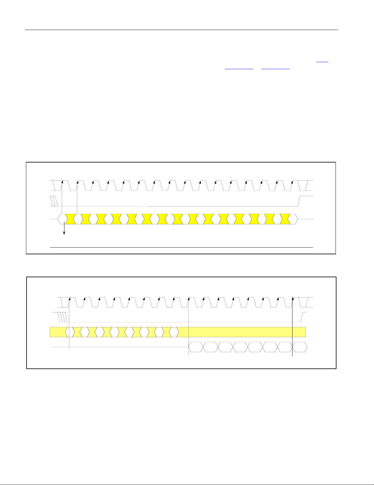
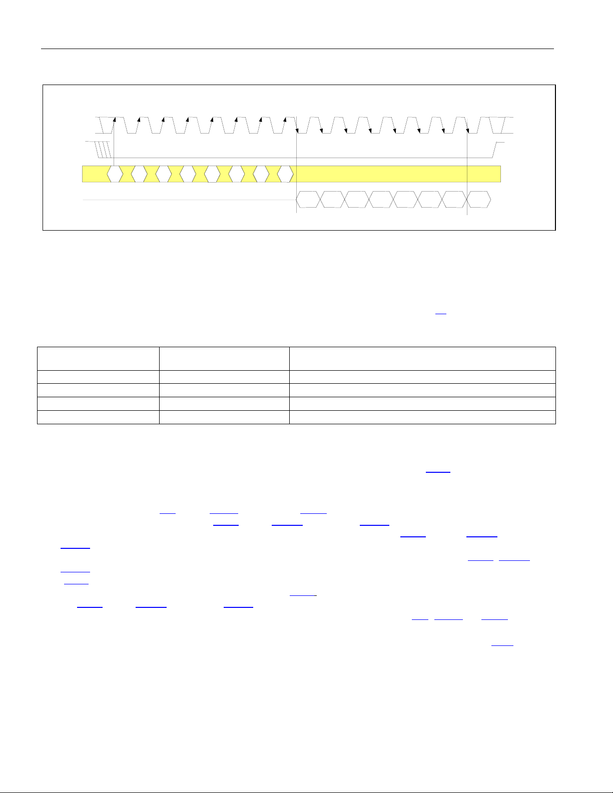
All data transfers are initiated by driving the CSB input low. When CLKE is low, SDO data is output on the rising
edge of SCLK and when CLKE is high, data is output on the falling edge of SCLK. Data is held until the next falling
or rising edge. All data transfers are terminated if CSB input transitions high. Port control logic is disabled and SDO
is tri-stated when CSB is high. SDI is always sampled on the rising edge of SCLK.
Figure 4-2. Serial Port Operation for Write Access
12345678910111213141516SCLK
CSB
SDI
DO D6
A1 A2 A3 A4 A5 A6 X
0
(lsb)
WRITE ACCESS ENABLED
SDO
(msb)
D1 D2 D3 D4 D5 D7
(lsb) (msb)
Figure 4-3. Serial Port Operation for Read Access with CLKE = 0
1234 56789 10111213141516
SCLK
CSB
SDI
X
A6
(msb)
D1 D2 D3 D4 D5 D6
D0
(lsb)
SDO
0
Read
Access
Enabled
A1 A2 A3 A4 A5
(lsb)
D7
(msb)
21 of 101
Page 22
DS26303: 3.3V, T1/E1/J1, Short-Haul, Octal Line Interface Unit
Figure 4-4. Serial Port Operation for Read Access with CLKE = 1
SCLK
123456 78910111213141516
CSB
SDI
A1 A2 A3 A4 A5
0
(lsb)
SDO
4.1.3 Parallel Port Operation
When using the parallel interface on the DS26303 the user has the option for either multiplexed bus operation or
non-multiplexed bus operation. The ALE pin is pulled high in non-multiplexed bus operation. The DS26303 can
operate with either Intel or Motorola bus-timing configurations selected by MOTEL pin. This pin being high selects
the Intel mode. The parallel port is only operational if the MODESEL pin is pulled high. The following table lists all
the pins and their functions in the parallel port mode. See the timing diagrams in Section
X
A6
(msb)
D0
(lsb)
D1
D2
D3 D4 D5
D7
D6
(msb)
10 for more details.
Table 4-3. Parallel Port Mode Selection and Pin Functions
MODESEL, MOTEL,
MUX
100 Non-multiplexed Motorola
110 Non-multiplexed Intel
101 Multiplexed Motorola
111 Multiplexed Intel
4.1.4 Interrupt Handling
INTB must be pulled high externally with a 10kΩ resistor for wired-OR operation. If a wired-OR operation is not
required, the INTB pin can be configured to be high when not active by setting register
There are three events that can potentially trigger an interrupt: a loss of signal (LOS), driver fault monitor (DFM), or
an alarm indication signal (AIS). The interrupt functions as follows:
• When a status bit (
corresponding interrupt status bit (
low if the event is enabled through the corresponding interrupt-enable bit (
LOSIE:LOSIEn).
• When an interrupt occurs, the host processor must read the three interrupt status registers (
LOSIS) to determine the source of the interrupt. If the interrupt status registers are set for clear-on-read
GISC.CWE reset), the read also clears the interrupt status register, which clears the output INTB pin. If the
(
interrupt status registers are set for clear-on-write (
AISIS:AISIn, DFMIS:DFMISn, or LOSIS:LOSISn) in order to clear it, which clears the output INTB pin.
bit (
• Subsequently, the host processor can read the corresponding status register (
the real-time status of the event.
Note: The BERT can also generate an interrupt. The BERT interrupt handling is described in Section
PARALLEL HOST
INTERFACE
ADDRESS, DATA, AND CONTROL
CSB, ACKB, DSB, RWB, ASB, A[4:0], D[7:0], INTB
CSB, RDY, WRB, RDB, ALE, A[4:0], D[7:0], INTB
CSB, ACKB, DSB, RWB, ASB, AD[7:0], INTB
CSB, RDY, WRB, RDB, ALE, AD[7:0], INTB
GISC.INTM.
AIS:AISn, DFMS:DFMSn, or LOSS:LOSn) changes on an interruptible event, the
AISIS:AISIn, DFMIS:DFMISn, or LOSIS:LOSISn) is set. The INTB pin will go
AISIE:AISIEn, DFMIE:DFMIEn, or
AISIS, DFMIS, and
GISC.CWE set), a 1 must be written to the interrupt status
AIS, DFMS, or LOSS) to check
6.9.2.
22 of 101
Page 23
DS26303: 3.3V, T1/E1/J1, Short-Haul, Octal Line Interface Unit
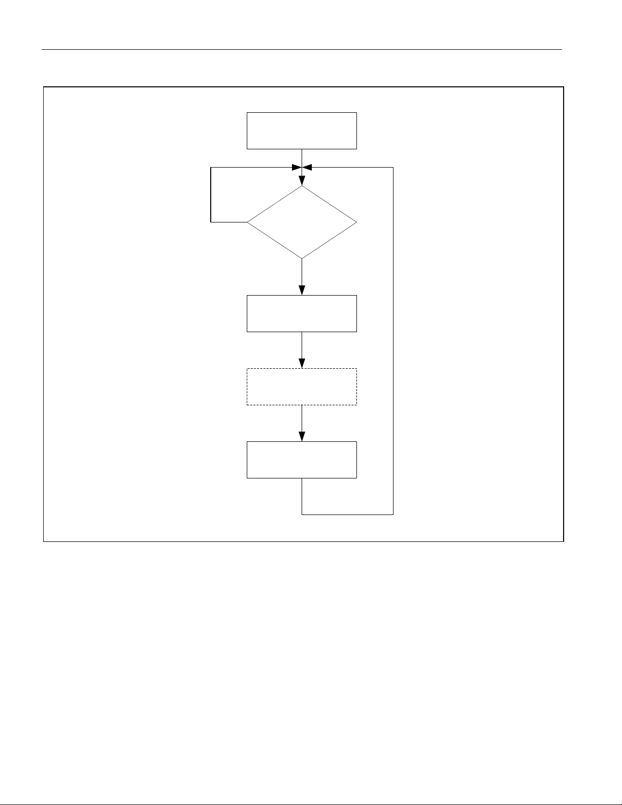
Figure 4-5. Interrupt Handling Flow Diagram
Interrupt Allowed
No
Interrupt Conditon
Read Interrupt Status
Register
Read Corresponding Status
Register (Optional)
Service the Interrupt
Exist?
Yes
23 of 101
Page 24

DS26303: 3.3V, T1/E1/J1, Short-Haul, Octal Line Interface Unit
5 REGISTERS
Five address bits are used to control the settings of the registers. AD[4:0] are used in both the parallel
nonmultiplexed mode and in multiplexed mode. In serial mode, the address is input serially on SDI. The register
space contains control for channels 1 to 8 from address 00 hex to 1F hex. The
pointer to access the different banks of registers. This register must be set to AA hex for access of the secondary
bank of registers, 01 hex for access to the individual LIU bank of registers, and 02 hex for access of the BERT
bank of registers. The primary bank of registers is accessed upon reset of this register to 00 hex.
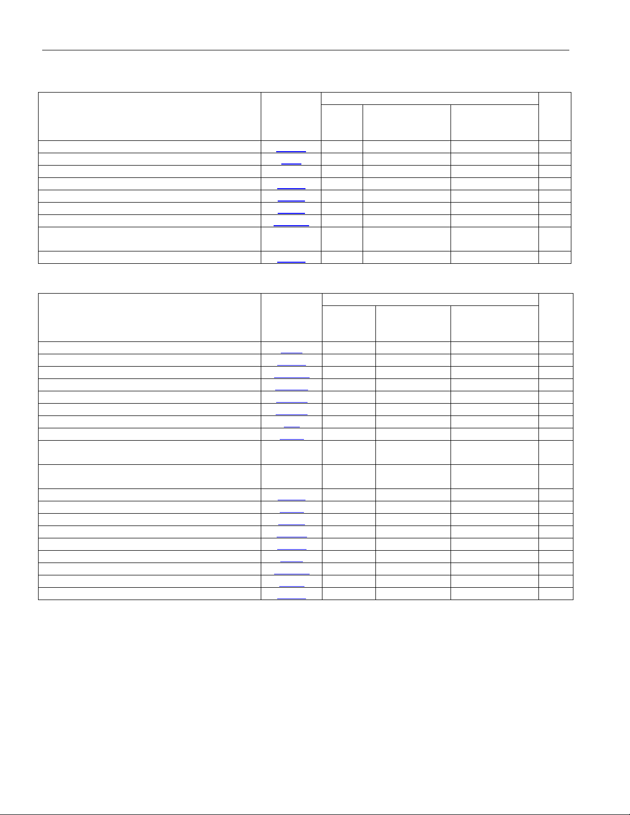
Table 5-1. Primary Register Set
ADDRESS
REGISTER NAME
Identification ID 00 xxx00000 xx00000 R
Analog Loopback Configuration ALBC 01 xxx00001 xx00001 RW
Remote Loopback Configuration RLBC 02 xxx00010 xx00010 RW
Transmit All-Ones Enable TAOE 03 xxx00011 xx00011 RW
Loss-of-Signal Status LOSS 04 xxx00100 xx00100 RW
Driver Fault Monitor Status DFMS 05 xxx00101 xx00101 RW
Loss-of-Signal Interrupt Enable LOSIE 06 xxx00110 xx00110 RW
Driver Fault Monitor Interrupt Enable DFMIE 07 xxx00111 xx00111 RW
Loss-of-Signal Interrupt Status LOSIS 08 xxx01000 xx01000 R
Driver Fault Monitor Interrupt Status DFMIS 09 xxx01001 xx01001 R
Software Reset SWR 0A xxx01010 xx01010 W
G.772 Monitor Control GMC 0B xxx01011 xx01011 RW
Digital Loopback Configuration DLBC 0C xxx01100 xx01100 RW
LOS/AIS Criteria Selection LASCS 0D xxx01101 xx01101 RW
Automatic Transmit All-Ones Select ATAOS 0E xxx01110 xx01110 RW
Global Configuration GC 0F xxx01111 xx01111 RW
Template Select Transceiver TST 10 xxx10000 xx10000 RW
Template Select TS 11 xxx10001 xx10001 RW
Output-Enable Bar OEB 12 xxx10010 xx10010 RW
Alarm Indication Signal Status AIS 13 xxx10011 xx10011 R
AIS Interrupt Enable AISIE 14 xxx10100 xx10100 RW
AIS Interrupt Status AISIS 15 xxx10101 xx10101 R
Reserved — 16–1E
Address Pointer for Bank Selection ADDP 1F xxx11111 xx11111 RW
HEX
PARALLEL
INTERFACE
A[7:0] (HEX)
xxx10110–
xxx11110
ADDP (1F) register is used as a
SERIAL
INTERFACE
A[7:1] (HEX)
xx10110–
xx11110
RW
—
24 of 101
Page 25
DS26303: 3.3V, T1/E1/J1, Short-Haul, Octal Line Interface Unit
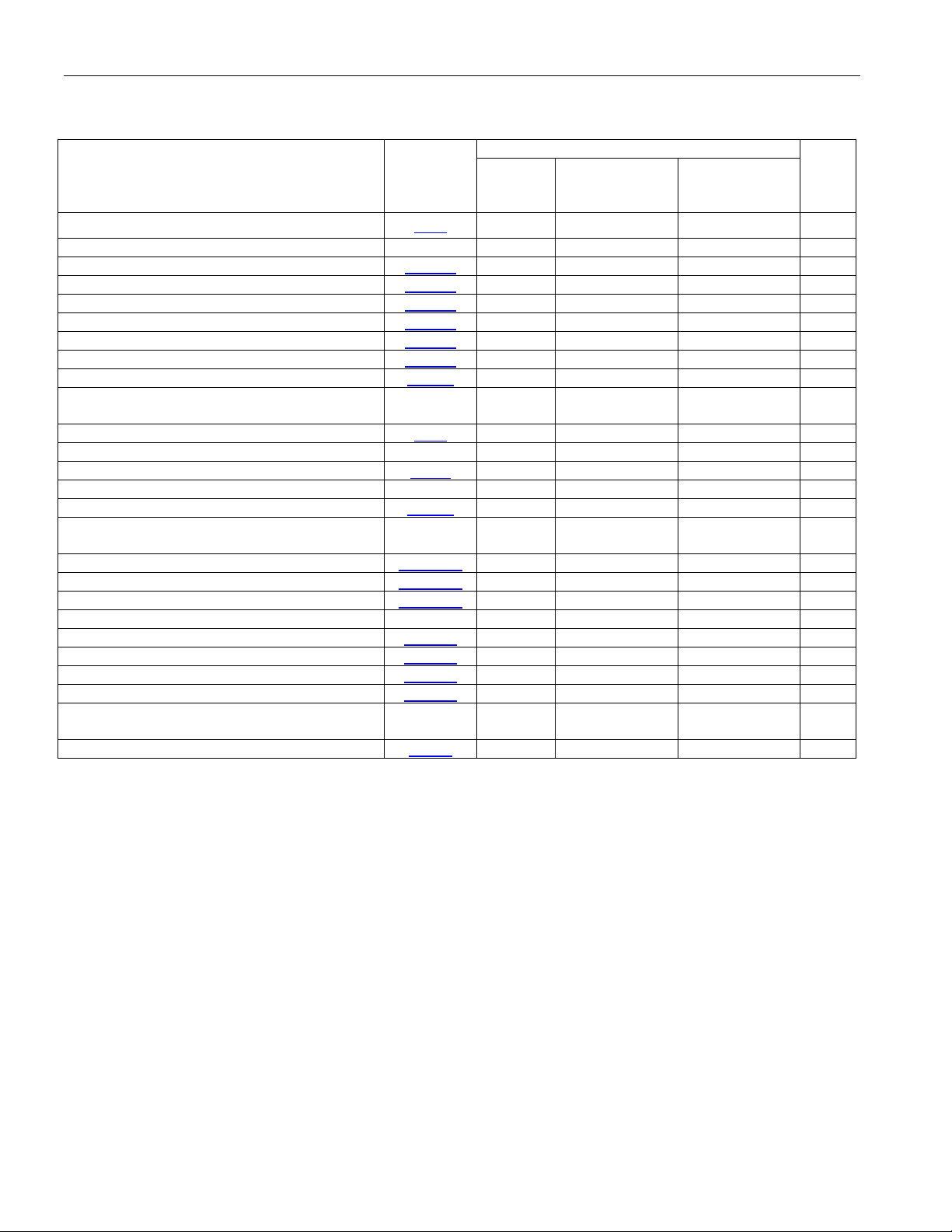
Table 5-2. Secondary Register Set
ADDRESS
REGISTER NAME
Single-Rail Mode Select SRMS 00 xxx00000 xx00000 RW
Line Code Selection LCS 01 xxx00001 xx00001 RW
Reserved — 02 xxx00010 xx00010 —
Receive Power-Down Enable RPDE 03 xxx00011 xx00011 RW
Transmit Power-Down Enable TPDE 04 xxx00100 xx00100 RW
Excessive Zero Detect Enable EZDE 05 xxx00101 xx00101 RW
Code Violation Detect Enable Bar CVDEB 06 xxx00110 xx00110 RW
Reserved — 07–1E
Address Pointer for Bank Selection ADDP 1F xxx11111 xx11111 RW
HEX
PARALLEL
INTERFACE
A[7:0] (HEX)
xxx00111–
xxx11110
SERIAL
INTERFACE
A[7:1] (HEX)
xx00111–
xx11110
RW
—
Table 5-3. Individual LIU Register Set
ADDRESS
REGISTER NAME
Individual Jitter Attenuator Enable IJAE 00 xxx00000 xx00000 RW
Individual Jitter Attenuator Position Select IJAPS 01 xxx00001 xx00001 RW
Individual Jitter Attenuator FIFO Depth Select IJAFDS 02 xxx00010 xx00010 RW
Individual Jitter Attenuator FIFO Limit Trip IJAFLT 03 xxx00011 xx00011 R
Individual Short Circuit Protection Disabled ISCPD 04 xxx00100 xx00100 RW
Individual AIS Select IAISEL 05 xxx00101 xx00101 RW
Master Clock Select MC 06 xxx00110 xx00110 RW
Global Management Register GMR 07 xxx00111 xx00111 RW
Reserved — 08–0B
Reserved — 0C–0F
Bit Error Rate Tester Control BTCR 10 xxx10000 xx10000 RW
BPV Error Insertion BEIR 11 Xxx10001 xxx10001 RW
Line Violation Detect Status LVDS 12 xxx10010 xx10010 R
Receive Clock Invert RCLKI 13 xxx10011 xx10011 RW
Transmit Clock Invert TCLKI 14 xxx10100 xx10100 RW
Clock Control CCR 15 xxx10101 xx10101 RW
RCLK Disable Upon LOS RDULR 16 xxx10110 xx10110 RW
Global Interrupt Status Control GISC 1E xxx11110 xx11110 RW
Address Pointer for Bank Selection ADDP 1F xxx11111 xx11111 RW
HEX
PARALLEL
INTERFACE
A[7:0] (HEX)
xxx01000–
xxx01011
xxx01100–
xxx01111
SERIAL
INTERFACE
A[7:1] (HEX)
xx01000–
xx01011
xx01100–
xx01111
RW
RW
R
25 of 101
Page 26
DS26303: 3.3V, T1/E1/J1, Short-Haul, Octal Line Interface Unit
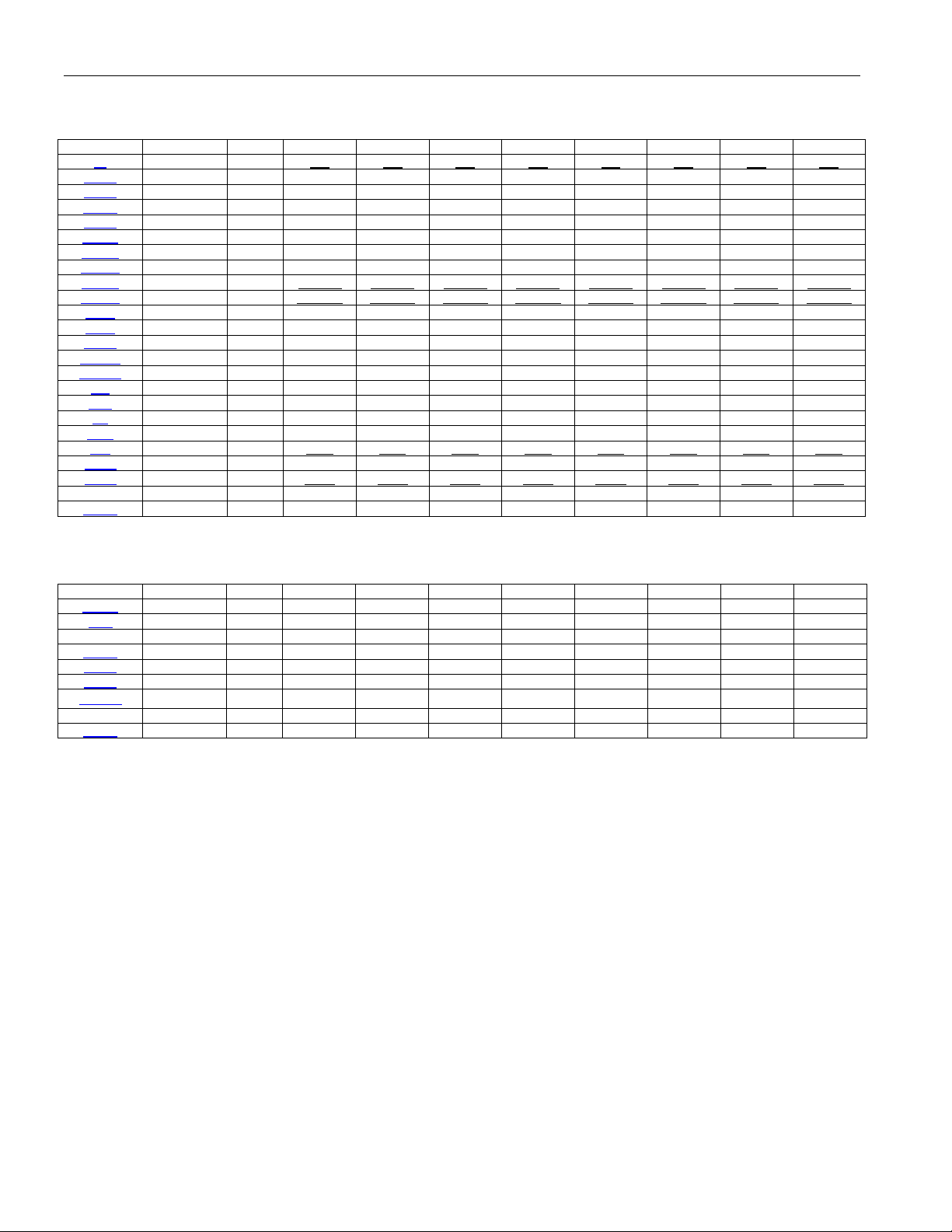
Table 5-4. BERT Register Set
ADDRESS
REGISTER NAME
BERT Control BCR 00 xxx00000 xx00000 RW
Reserved — 01 xxx00001 xx00001
BERT Pattern Configuration 1 BPCR1 02 xxx00010 xx00010 RW
BERT Pattern Configuration 2 BPCR2 03 xxx00011 xx00011 RW
BERT Seed/Pattern 1 BSPR1 04 xxx00100 xx00100 RW
BERT Seed/Pattern 2 BSPR2 05 xxx00101 xx00101 RW
BERT Seed/Pattern 3 BSPR3 06 xxx00110 xx00110 RW
BERT Seed/Pattern 4 BSPR4 07 xxx00111 xx00111 RW
Transmit Error-Insertion Control TEICR 08 xxx01000 xx01000 RW
Reserved — 09–0B
BERT Status BSR 0C xxx01100 xx01100 R
Reserved — 0D xxx01101 xx01101 —
BERT Status Register Latched BSRL 0E xxx01110 xx01110 RW
Reserved — 0F xxx01111 xx01111 —
BERT Status Register Interrupt Enable BSRIE 10 xxx10000 xx10000 RW
Reserved — 11–13
Receive Bit-Error Count Register 1 RBECR1 14 xxx10100 xx10100 R
Receive Bit-Error Count Register 2 RBECR2 15 xxx10101 xx10101 R
Receive Bit-Error Count Register 3 RBECR3 16 xxx10110 xx10110 R
Reserved — 17 xxx10111 xx10111 —
Receive Bit Count Register 1 RBCR1 18 xxx11000 xx11000 R
Receive Bit Count Register 2 RBCR2 19 xxx11001 xx11001 R
Receive Bit Count Register 3 RBCR3 1A xxx11010 xx11010 R
Receive Bit Count Register 4 RBCR4 1B xxx11011 xx11011 R
Reserved — 1C–1E
Address Pointer for Bank Selection ADDP 1F xxx11111 xx11111 RW
HEX
PARALLEL
INTERFACE
A7–A0 (HEX)
xxx01001–
xxx01010
xxx10001–
xxx10011
xxx11100–
xxx11110
SERIAL
INTERFACE
A7–A1 (HEX)
xx01001–
xx01010—
xx10001–
xx10011
xx11100–
xx11110
RW
—
—
—
26 of 101
Page 27
DS26303: 3.3V, T1/E1/J1, Short-Haul, Octal Line Interface Unit
Table 5-5. Primary Register Set Bit Map
REGISTER ADDRESS TYPE BIT 7 BIT 6 BIT 5 BIT 4 BIT 3 BIT 2 BIT 1 BIT 0
ID 00 R ID7 ID6 ID5 ID4 ID3 ID2 ID1 ID0
ALBC 01 RW ALBC8 ALBC7 ALBC6 ALBC5 ALBC4 ALBC3 ALBC2 ALBC1
RLBC 02 RW RLBC8 RLBC7 RLBC6 RLBC5 RLBC4 RLBC3 RLBC2 RLBC1
TAOE 03 RW TAOE8 TAOE7 TAOE6 TAOE5 TAOE4 TAOE3 TAOE2 TAOE1
LOSS 04 RW LOSS8 LOSS7 LOSS6 LOSS5 LOSS4 LOSS3 LOSS2 LOSS1
DFMS 05 RW DFMS8 DFMS7 DFMS6 DFMS5 DFMS4 DFMS3 DFMS2 DFMS1
LOSIE 06 RW LOSIE8 LOSIE7 LOSIE6 LOSIE5 LOSIE4 LOSIE3 LOSIE2 LOSIE1
DFMIE 07 RW DFMIE8 DFMIE7 DFMIE6 DFMIE5 DFMIE4 DFMIE3 DFMIE2 DFMIE1
LOSIS 08 R LOSIS8 LOSIS7 LOSIS6 LOSIS5 LOSIS4 LOSIS3 LOSIS2 LOSIS1
DFMIS 09 R DFMIS8 DFMIS7 DFMIS6 DFMIS5 DFMIS4 DFMIS3 DFMIS2 DFMIS1
SWR 0A W SWR8 SWR7 SWR6 SWR5 SWR4 SWR3 SWR2 SWR1
GMC 0B RW BERTDIR BMCKS BTCKS — GMC3 GMC2 GMC1 GMC0
DLBC 0C RW DLBC8 DLBC7 DLBC6 DLBC5 DLBC4 DLBC3 DLBC2 DLBC1
LASCS 0D RW LASCS8 LASCS7 LASCS6 LASCS5 LASCS4 LASCS3 LASCS2 LASCS1
ATAOS 0E RW ATAOS8 ATAOS7 ATAOS6 ATAOS5 ATAOS4 ATAOS3 ATAOS2 ATAOS1
GC 0F RW RIMPMS AISEL SCPD CODE JADS — JAPS JAE
TST 10 RW — — — — — TST2 TST1 TST0
TS 11 RW RIMPOFF TIMPOFF — — TIMPRM TS2 TS1 TS0
OEB 12 RW OEB8 OEB7 OEB6 OEB5 OEB4 OEB3 OEB2 OEB1
AIS 13 R AIS8 AIS7 AIS6 AIS5 AIS4 AIS3 AIS2 AIS1
AISIE 14 RW AISIE8 AISIE7 AISIE6 AISIE5 AISIE4 AISIE3 AISIE2 AISIE1
AISIS 15 R AISI8 AISI7 AISI6 AISI5 AISI4 AISI3 AISI2 AISI1
Reserved 16-1E — — — — — — — — —
ADDP 1F RW ADDP7 ADDP6 ADDP5 ADDP4 ADDP3 ADDP2 ADDP1 ADDP0
Note: Underlined bits are read-only.
Table 5-6. Secondary Register Set Bit Map
REGISTER ADDRESS TYPE BIT 7 BIT 6 BIT 5 BIT 4 BIT 3 BIT 2 BIT 1 BIT 0
SRMS 00 RW SRMS8 SRMS7 SRMS6 SRMS5 SRMS4 SRMS3 SRMS2 SRMS1
LCS 01 RW LCS8 LCS7 LCS6 LCS5 LSC4 LCS3 LSC2 LSC1
Reserved 02 RW — — — — — — — —
RPDE 03 RW RPDE8 RPDE7 RPDE6 RPDE5 RPDE4 RPDE3 RPDE2 RPDE1
TPDE 04 RW TPDE8 TDPE7 TPDE6 TPDE5 TPDE4 TPDE3 TPDE2 TPDE1
EZDE 05 RW EZDE8 EZDE7 EZDE6 EZDE5 EZDE4 EZDE3 EZDE2 EZDE1
CVDEB 06 RW CVDEB8 CVDEB7 CVDEB6 CVDEB5 CVDEB4 CVDEB3 CVDEB2 CVDEB1
Reserved 07-1E — — — — — — — — —
ADDP 1F RW ADDP7 ADDP6 ADDP5 ADDP4 ADDP3 ADDP2 ADDP1 ADDP0
27 of 101
Page 28
DS26303: 3.3V, T1/E1/J1, Short-Haul, Octal Line Interface Unit
Table 5-7. Individual LIU Register Set Bit Map
REGISTER ADDRESS TYPE BIT 7 BIT 6 BIT 5 BIT 4 BIT 3 BIT 2 BIT 1 BIT 0
IJAE 00 RW IJAE8 IJAE7 IJAE6 IJAE5 IJAE4 IJAE3 IJAE2 IJAE1
IJAPS 01 RW IJAPS8 IJAPS7 IJAPS6 IJAPS5 IJAPS4 IJAPS3 IJAPS2 IJAPS1
IJAFDS 02 RW IJAFDS8 IJAFDS7 IJAFDS6 IJAFDS5 IJAFDS4 IJAFDS3 IJAFDS2 IJAFDS1
IJAFLT 03 R IJAFLT8 IJAFLT7 IJAFLT6 IJAFLT5 IJAFLT4 IJAFLT3 IJAFLT2 IJAFLT1
ISCPD 04 RW ISCPD8 ISCPD7 ISCPD6 ISCPD5 ISCPD4 ISCPD3 ISCPD2 ISCPD1
IAISEL 05 RW IAISEL8 IAISEL7 IAISEL6 IAISEL5 IAISEL4 IAISEL3 IAISEL2 IAISEL1
MC 06 RW — PCLKI TECLKE CLKAE MPS1 MPS0 FREQS PLLE
GMR 07 RW — — — — — JABWS1 JABWS0 RHPMC
Reserved 08 RW — — — — — — — —
Reserved 09 RW — — — — — — — —
Reserved 0A RW — — — — — — — —
Reserved 0B RW — — — — — — — —
Reserved 0C R — — — — — — — —
Reserved 0D R — — — — — — — —
Reserved 0E R — — — — — — — —
Reserved 0F R — — — — — — — —
BTCR 10 RW BTS2 BTS1 BTS0 — — — — BERTE
BEIR 11 RW BEIR8 BEIR7 BEIR6 BEIR5 BEIR4 BEIR3 BEIR2 BEIR1
LVDS 12 R LVDS8 LVDS7 LVDS6 LVDS5 LVDS4 LVDS3 LVDS2 LVDS1
RCLKI 13 RW RCLKI8 RCLKI7 RCLKI6 RCLKI5 RCLKI4 RCLKI3 RCLKI2 RCLKI1
TCLKI 14 RW TCLKI8 TCLKI7 TCLKI6 TCLKI5 TCLKI4 TCLKI3 TCLKI2 TCLKI1
CCR 15 RW PCLKS2 PCLKS1 PCLKS0 TECLKS CLKA3 CLKA2 CLKA1 CLKA0
RDULR 16 RW RDULR8 RDULR7 RDULR6 RDULR5 RDULR4 RDULR3 RDULR2 RDULR1
GISC 1E RW — — — — — — INTM CWE
ADDP 1F RW ADDP7 ADDP6 ADDP5 ADDP4 ADDP3 ADDP2 ADDP1 ADDP0
Note: Underlined bits are read-only.
Table 5-8. BERT Register Bit Map
REGISTER ADDRESS TYPE BIT 7 BIT 6 BIT 5 BIT 4 BIT 3 BIT 2 BIT 1 BIT 0
BCR 00 RW PMUM LPMU RNPL RPIC MPR APRD TNPL TPIC
Reserved 01 — — — — — — — — —
BPCR1 02 RW — QRSS PTS PLF4 PLF3 PLF2 PLF1 PLF0
BPCR2 03 RW — — — PTF4 PTF3 PTF2 PTF1 PTF0
BSPR1 04 RW BSP7 BSP6 BSP5 BSP4 BSP3 BSP2 BSP1 BSP0
BSPR2 05 RW BSP15 BSP14 BSP13 BSP12 BSP11 BSP10 BSP9 BSP8
BSPR3 06 RW BSP23 BSP22 BSP21 BSP20 BSP19 BSP18 BSP17 BSP16
BSPR4 07 RW BSP31 BSP30 BSP29 BSP28 BSP27 BSP26 BSP25 BSP24
TEICR 08 RW — — TEIR2 TEIR1 TEIR0 BEI TSEI MEIMS
Reserved 09–0B — — — — — — — — —
BSR 0C R — — — — PMS — BEC OOS
Reserved 0D — — — — — — — — —
BSRL 0E R — — — — PMSL BEL BECL OOSL
Reserved 0F — — — — — — — — —
BSRIE 10 RW — — — — PMSIE BEIE BECIE OOSIE
Reserved 11–13 — — — — — — — — —
RBECR1 14 R BEC7 BEC6 BEC5 BEC4 BEC3 BEC2 BEC1 BEC0
RBECR2 15 R BEC15 BEC14 BEC13 BEC12 BEC11 BEC10 BEC9 BEC8
RBECR3 16 R BEC23 BEC22 BEC21 BEC20 BEC19 BEC18 BEC17 BEC16
Reserved 17 — — — — — — — — —
RBCR1 18 R BC7 BC6 BC5 BC4 BC3 BC2 BC1 BC0
RBCR2 19 R BC15 BC14 BC13 BC12 BC11 BC10 BC9 BC8
RBCR3 1A R BC23 BC22 BC21 BC20 BC19 BC18 BC17 BC16
RBCR4 1B R BC31 BC30 BC29 BC28 BC27 BC26 BC25 BC24
Reserved 1C–1E — — — — — — — — —
ADDP 1F RW ADDP7 ADDP6 ADDP5 ADDP4 ADDP3 ADDP2 ADDP1 ADDP0
Note: Underlined bits are read-only.
28 of 101
Page 29

DS26303: 3.3V, T1/E1/J1, Short-Haul, Octal Line Interface Unit
5.1 Register Description
This section details the register description of each bit. Whenever the variable “n” in italics is used in any of the
register descriptions, it represents 1, 2, 3, 4, 5, 6, 7, and 8.
5.1.1 Primary Registers
Register Name:
Register Description:
Register Address:
Bit # 7 6 5 4 3 2 1 0
Name ID7
Bit 7: Device CODE ID Bit 7 (ID7). This bit is zero for the 75Ω impedance part number and one for the 120Ω
impedance part number.
Bits 6 to 3: Device CODE ID Bits 6 to 3 (ID6 to ID3). These bits tell the user the number of ports the device
contains.
Bits 2 to 0: Device CODE ID Bits 2 to 0 (ID2 to ID0). These bits tell the user the revision of the part. Contact the
factory for details.
ID6 ID5 ID4 ID3 ID2 ID1 ID0
ID
Identification Register
00h
Register Name:
Register Description:
Register Address:
Bit # 7 6 5 4 3 2 1 0
Name ALBC8 ALBC7 ALBC6 ALBC5 ALBC4 ALBC3 ALBC2 ALBC1
Default 0 0 0 0 0 0 0 0
Bits 7 to 0: Analog Loopback Configuration Bits Channel n (ALBCn). When this bit is set, LIUn is placed in
analog loopback. TTIPn and TRINGn are looped back to RTIPn and RRINGn. The data at RTIPn and RRINGn is
ignored. The LOS detector is still in operation. The jitter attenuator is in use if enabled for the transmitter or
receiver.
Register Name:
Register Description:
Register Address:
Bit # 7 6 5 4 3 2 1 0
Name RLBC8 RLBC7 RLBC6 RLBC5 RLBC4 RLBC3 RLBC2 RLBC1
Default 0 0 0 0 0 0 0 0
Bits 7 to 0: Remote Loopback Configuration Bits Channel n (RLBCn). When this bit is set, remote loopback is
enabled on LIUn. The analog-received signal goes through the receiver and is looped back to the transmitter. The
data at TPOSn and TNEGn is ignored. The jitter attenuator is in use if enabled. Note: LIUn is placed in dual
loopback if
DLBC:DLBCn is also set.
ALBC
Analog Loopback Configuration Register
01h
RLBC
Remote Loopback Configuration Register
02h
29 of 101
Page 30

DS26303: 3.3V, T1/E1/J1, Short-Haul, Octal Line Interface Unit
Register Name:
Register Description:
Register Address:
TAOE
Transmit All-Ones Enable Register
03h
Bit # 7 6 5 4 3 2 1 0
Name TAOE8 TAOE7 TAOE6 TAOE5 TAOE4 TAOE3 TAOE2 TAOE1
Default 0 0 0 0 0 0 0 0
Bits 7 to 0: Transmit All-Ones Enable Channel n (TAOEn). When this bit is set, a continuous stream of all ones
is sent on channel n (TTIPn and TRINGn). MCLK is used as a reference clock for the transmit all-ones signal. The
data arriving at TPOSn and TNEGn is ignored.
Register Name:
Register Description:
Register Address:
LOSS
Loss-of-Signal Status Register
04h
Bit # 7 6 5 4 3 2 1 0
Name LOSS8
LOSS7 LOSS6 LOSS5 LOSS4 LOSS3 LOSS2 LOSS1
Default 0 0 0 0 0 0 0 0
Bits 7 to 0: Loss-of-Signal Status Channel n (LOSSn). When this bit is set, an LOS condition has been detected
on LIUn. The criteria and conditions of LOS are described in Section
6.4.3: Loss of Signal.
Register Name:
Register Description:
Register Address:
DFMS
Driver Fault Monitor Status Register
05h
Bit # 7 6 5 4 3 2 1 0
Name DFMS8
DFMS7 DFMS6 DFMS5 DFMS4 DFMS3 DFMS2 DFMS1
Default 0 0 0 0 0 0 0 0
Bits 7 to 0: Driver Fault Monitor Status Channel n (DFMSn). When this bit is set, it indicates that there is a short
or open circuit at the transmit driver for LIUn.
Register Name:
Register Description:
Register Address:
LOSIE
Loss-of-Signal Interrupt Enable Register
06h
Bit # 7 6 5 4 3 2 1 0
Name LOSIE8 LOSIE7 LOSIE6 LOSIE5 LOSIE4 LOSIE3 LOSIE2 LOSIE1
Default 0 0 0 0 0 0 0 0
Bits 7 to 0: Loss-of-Signal Interrupt Enable Channel n (LOSIEn). When this bit is set, a change in the LOS
status for LIUn can generate an interrupt.
30 of 101
Page 31

DS26303: 3.3V, T1/E1/J1, Short-Haul, Octal Line Interface Unit
Register Name:
Register Description:
Register Address:
DFMIE
Driver Fault Monitor Interrupt Enable Register
07h
Bit # 7 6 5 4 3 2 1 0
Name DFMIE8 DFMIE7 DFMIE6 DFMIE5 DFMIE4 DFMIE3 DFMIE2 DFMIE1
Default 0 0 0 0 0 0 0 0
Bits 7 to 0: Driver Fault Monitor Interrupt Enable Channel n (DFMIEn). When this bit is set, a change in DFM
status can generate an interrupt in monitor n.
Register Name:
Register Description:
Register Address:
LOSIS
Loss-of-Signal Interrupt Status Register
08h
Bit # 7 6 5 4 3 2 1 0
Name LOSIS8
LOSIS7 LOSIS6 LOSIS5 LOSIS4 LOSIS3 LOSIS2 LOSIS1
Default 0 0 0 0 0 0 0 0
Bits 7 to 0: Loss-of-Signal Interrupt Status Channel n (LOSISn). When this bit is set, it indicates an LOS status
has transitioned from a 0 to 1 or 1 to 0 and was detected for LIUn. The interrupt for LIUn is enabled in
bit when latched is cleared by a read operation to the register if
cleared by a write operation to the bit if
GISC.CWE is set.
GISC.CWE is reset. This bit, when latched, is
LOSIS. This
Register Name:
Register Description:
Register Address:
DFMIS
Driver Fault Monitor Interrupt Status Register
09h
Bit # 7 6 5 4 3 2 1 0
Name DFMIS8
DFMIS7 DFMIS6 DFMIS5 DFMIS4 DFMIS3 DFMIS2 DFMIS1
Default 0 0 0 0 0 0 0 0
Bits 7 to 0: Driver Fault Status Register Channel n (DFMISn). When this bit is set, it indicates a DFM status has
transitioned from 0 to 1 or 1 to 0 and was detected for LIUn. The interrupt for LIUn is enabled by in
when latched is cleared by a read operation to the register if
by a write operation to the bit if
GISC.CWE is set.
GISC.CWE is reset. This bit, when latched, is cleared
DFMIE. This bit
Register Name:
Register Description:
Register Address:
SWR
Software Reset Register
0Ah
Bit # 7 6 5 4 3 2 1 0
Name SWR8 SWR7 SWR6 SWR5 SWR4 SWR3 SWR2 SWR1
Default 0 0 0 0 0 0 0 0
Bits 7 to 0: Software Reset (SWR). Whenever any write is performed to this register, at least a 1μs reset will be
generated that resets the DS26303. All the registers will be restored to their default values. A read operation will
always read back all zeros.
31 of 101
Page 32

DS26303: 3.3V, T1/E1/J1, Short-Haul, Octal Line Interface Unit
Register Name:
Register Description:
Register Address:
Bit # 7 6 5 4 3 2 1 0
Name BERTDIR BMCKS BTCKS — GMC3 GMC2 GMC1 GMC0
Default 0 0 0 0 0 0 0 0
Bit 7: BERT Direction Select (BERTDIR). When set, the internal BERT will output its data on RPOS/RNEG rather
than TTIP/TRING. The BERT will use the recovered clock unless BMCKS or BTCKS is set.
Bit 6: BERT MCLK Select (BMCKS). When set, while BERTDIR is set and BTCKS is not set, the internal BERT
will use MCLK rather than the recovered clock.
Bit 5: BERT Direction Select (BTCKS). When set, while BERTDIR is set, the internal BERT will use TCLK rather
than the recovered clock or MCLK.
Bits 3 to 0: G.772 Monitoring Control (GMC). These bits are used to select a transmit line (TTIPn/TRINGn) or
receive line (RTIPn/RRINGn) for nonintrusive monitoring. Receiver 1 is used to monitor channels 2 to 8. See
.
5-9
GMC
G.772 Monitoring Control Register
0Bh
Table
Table 5-9. G.772 Monitoring Control
GMC3 GMC2 GMC1 GMC0 SELECTION
0 0 0 0 No Monitoring
0 0 0 1 Receive Line 2
0 0 1 0 Receive Line 3
0 0 1 1 Receive Line 4
0 1 0 0 Receive Line 5
0 1 0 1 Receive Line 6
0 1 1 0 Receive Line 7
0 1 1 1 Receive Line 8
1 0 0 0 No Monitoring
1 0 0 1 Transmit Line 2
1 0 1 0 Transmit Line 3
1 0 1 1 Transmit Line 4
1 1 0 0 Transmit Line 5
1 1 0 1 Transmit Line 6
1 1 1 0 Transmit Line 7
1 1 1 1 Transmit Line 8
32 of 101
Page 33

DS26303: 3.3V, T1/E1/J1, Short-Haul, Octal Line Interface Unit
Register Name:
Register Description:
Register Address:
DLBC
Digital Loopback Configuration Register
0Ch
Bit # 7 6 5 4 3 2 1 0
Name DLBC8 DLBC7 DLBC6 DLBC5 DLBC4 DLBC3 DLBC2 DLBC1
Default 0 0 0 0 0 0 0 0
Bits 7 to 0: Digital Loopback Configuration Channel n (DLBCn). When this bit is set, the LIUn is placed in
digital loopback. The data at TPOSn/TNEGn is encoded and looped back to the decoder and output on
RPOSn/RNEGn. The jitter attenuator can optionally be included in the transmit or receive paths. Note: LIUn is
placed in dual loopback if
RLBC:RLBCn is also set.
Register Name:
Register Description:
Register Address:
LASCS
LOS/AIS Criteria Selection Register
0Dh
Bit # 7 6 5 4 3 2 1 0
Name LASCS8 LASCS7 LASCS6 LASCS5 LASCS4 LASCS3 LASCS2 LASCS1
Default 0 0 0 0 0 0 0 0
Bits 7 to 0: LOS/AIS Criteria Selection Channel n (LASCSn). This bit is used for LOS/AIS selection criteria for
LIUn. In E1 mode if set, these bits use ETS 300 233 mode selections. If reset, these bits use G.775 criteria. In
T1/J1 mode, T1.231 criteria is selected.
33 of 101
Page 34

DS26303: 3.3V, T1/E1/J1, Short-Haul, Octal Line Interface Unit
Register Name:
Register Description:
Register Address:
ATAOS
Automatic Transmit All-Ones Select Register
0Eh
Bit # 7 6 5 4 3 2 1 0
Name ATAOS8 ATAOS7 ATAOS6 ATAOS5 ATAOS4 ATAOS3 ATAOS2 ATAOS1
Default 0 0 0 0 0 0 0 0
Bit 7 to 0: Automatic Transmit All-Ones Select Channel n (ATAOSn). When this bit is set an all-ones signal is
sent if a loss of signal is detected for LIUn. The all-ones signal uses MCLK as the reference clock.
Register Name:
Register Description:
Register Address:
GC
Global Configuration Register
0Fh
Bit # 7 6 5 4 3 2 1 0
Name RIMPMS AISEL SCPD CODE JADS — JAPS JAE
Default 0 0 0 0 0 0 0 0
Bit 7: Receive Impedance Mode Select (RIMPMS). When this bit is set, the internal impedance mode is selected,
so all receive lines (RTIPn and RINGn) require no external resistance component. When this mode is selected, the
die-attach pad on the bottom of the package should be connected to ground for thermal dissipation. When reset,
external impedance mode is selected so all receive lines (RTIPn and RINGn) require external resistance. Note that
when in external impedance mode, if
TS.RIMPOFF is reset, the resistance is still adjusted internally for the T1
(100Ω), J1 (110Ω), and E1(75Ω) modes of operation by the template selected so that only one resistor value is
required externally. In E1 (120Ω), external impedance mode has no need for any internal adjustment.
Bit 6: AIS Enable During Loss (AISEL). When this bit is set, for all channels, an AIS is sent to the system side
upon detecting an LOS on the corresponding channel. The individual settings in the
when this bit is set. When reset, the
IAISEL register has control.
IAISEL register are ignored
Bit 5: Short-Circuit-Protection Disable (SCPD). If this bit is set, the short-circuit protection is disabled for all the
transmitters. The individual settings in
ISCPD are ignored when this bit is set. When reset, the ISCPD register has
control.
Bit 4: Code (CODE). If this bit is set, AMI encoding/decoding is selected. The individual settings in register
are ignored when this bit is set. If reset, the
LCS register has control.
LCS
Bit 3: Jitter Attenuator Depth Select (JADS). If this bit is set the jitter attenuator FIFO depth is 128 bits. The
individual settings in register
IJAFDS are ignored if this bit is set. If reset, the IJAFDS register has control.
Bit 1: Jitter Attenuator Position Select (JAPS). When the JAPS bit is set high, the jitter attenuator is in the
receive path, and when it is set low, it is in the transmit path. The individual settings in register
this bit is set. If reset, the
IJAPS register has control.
IJAPS are ignored if
Bit 0: Jitter Attenuator Enable (JAE). When this bit is set the jitter attenuator is enabled. The individual settings in
register
IJAE are ignored if this bit is set. If reset, the IJAE register has control.
34 of 101
Page 35

DS26303: 3.3V, T1/E1/J1, Short-Haul, Octal Line Interface Unit
Register Name:
Register Description:
Register Address:
TST
Template Select Transceiver Register
10h
Bit # 7 6 5 4 3 2 1 0
Name — — — — — TST2 TST1 TST0
Default 0 0 0 0 0 0 0 0
Bits 2 to 0: TST Template Select Transceiver [2:0] (TST [2:0]). TST[2:0] is used to select the transceiver that the
transmit template select register (hex 11) applies to. See
Table 5-10.
Table 5-10. TST Template Select Transceiver Register
TST[2:0] CHANNEL TST[2:0] CHANNEL
000 1 100 5
001 2 101 6
010 3 110 7
011 4 111 8
Register Name:
Register Description:
Register Address:
Bit # 7 6 5 4 3 2 1 0
Name RIMPOFF TIMPOFF — — TIMPRM TS2 TS1 TS0
Default 0 0 — — 0 0 0 0
Bit 7: Receive Impedance Match Off (RIMPOFF). If this bit is set, all the receive impedance match is turned off.
TS
Template Select Register
11h
Bit 6: Transmit Impedance Termination Off (TIMPOFF). If this bit is set, all the internal transmit terminating
impedance is turned off.
Bit 3: Transmit Impedance Receive Match (TIMPRM). This bit selects the internal transmit termination
impedance and receive impedance match for E1 mode and T1/J1 mode. Note: If the part number ends with –120,
then the default is 120Ω and 75Ω when set for El mode only.
DEVICE BIT SETTING
E1 MODE (Ω) T1 MODE (Ω)
DS26303L-120 0 120 100
DS26303L-120 1 75 110
DS26303L-75 0 75 100
DS26303L-75 1 120 110
Bits 2 to 0: Template Selection [2:0] (TS[2:0]). Bits TS[2:0] are used to select E1 or T1/J1 mode, the template,
and the settings for various cable lengths. The impedance termination for the transmitter and impedance match for
the receiver are specified by bit TIMPRM. See
Table 5-11 for bit selection of TS[2:0].
Table 5-11. Template Selection
TS[2:0] LINE LENGTH
CABLE LOSS
(dB)
IMPEDANCE (Ω)
011 0–133ft. ABAM 0.6 100/110 T1/J1
100 133–266ft. ABAM 1.2 100/110 T1
101 266–399ft. ABAM 1.8 100/110 T1
110 399–533ft. ABAM 2.4 100/110 T1
111 533–655ft. ABAM 3.0 100/110 T1
000 G.703 coaxial and twisted pair cable 75/120 E1
001 and 010 Reserved — — —
1
See TIMPRM bit in SWM or TIMPRM pin in HWM for transmit impedance and receive match selection.
1
OPERATION MODE
35 of 101
Page 36

DS26303: 3.3V, T1/E1/J1, Short-Haul, Octal Line Interface Unit
Register Name:
Register Description:
Register Address:
OEB
Output-Enable Bar Register
12h
Bit # 7 6 5 4 3 2 1 0
Name OEB8 OEB7 OEB6 OEB5 OEB4 OEB3 OEB2 OEB1
Default 0 0 0 0 0 0 0 0
Bits 7 to 0: Output-Enable Bar Channel n (OEBn). When this bit is set the transmitter output for LIUn is placed in
high impedance. Note that when the OE pin is low, it overrides the setting of this register.
Register Name:
Register Description:
Register Address:
AIS
Alarm Indication Signal Status Register
13h
Bit # 7 6 5 4 3 2 1 0
Name AIS8
AIS7 AIS6 AIS5 AIS4 AIS3 AIS2 AIS1
Default 0 0 0 0 0 0 0 0
Bits 7 to 0: Alarm Indication Signal Channel n (AISn). This bit is set when AIS is detected for LIUn. The criteria
for AIS selection is detailed in Section
6.4.4: AIS. The selection of the AIS criteria is done by settings in LASCS.
36 of 101
Page 37

DS26303: 3.3V, T1/E1/J1, Short-Haul, Octal Line Interface Unit
Register Name:
Register Description:
Register Address:
Bit # 7 6 5 4 3 2 1 0
Name AISIE8 AISIE7 AISIE6 AISIE5 AISIE4 AISIE3 AISIE2 AISIE1
Default 0 0 0 0 0 0 0 0
Bits 7 to 0: AIS Interrupt Mask Channel n (AISIEn). When this bit is set, interrupts can be generated for LIUn if
AIS status transitions.
Register Name:
Register Description:
Register Address:
Bit # 7 6 5 4 3 2 1 0
Name AISIS8
Default 0 0 0 0 0 0 0 0
Bits 7 to 0: AIS Interrupt Channel n (AISISn). This bit is set when AIS transitions from a 0 to 1 or 1 to 0. The
interupt for LIUn is enabled in
GISC.CWE is reset. This bit when latched is cleared by a write operation to the bit if GISC.CWE is set.
AISIS7 AISIS6 AISIS5 AISIS4 AISIS3 AISIS2 AISIS1
AISIE
AIS Interrupt Enable Register
14h
AISIS
AIS Interrupt Status Register
15h
AISIE. This bit when latched is cleared by a read operation to the register if
Register Name:
Register Description:
Register Address:
Bit # 7 6 5 4 3 2 1 0
Name ADDP7 ADDP6 ADDP5 ADDP4 ADDP3 ADDP2 ADDP1 ADDP0
Default 0 0 0 0 0 0 0 0
Bits 7 to 0: Address Pointer (ADDP). This pointer is used to switch between pointing to the primary registers, the
secondary registers, individual registers, and BERT registers. See
ADDP
Address Pointer for Bank Selection Register
1Fh
Table 5-12 for bank selection.
Table 5-12. Address Pointer for Bank Selection
ADDP[7:0] (HEX) BANK NAME
00 Primary Bank
AA Secondary Bank
01 Individual LIU Bank
02 BERT Bank
37 of 101
Page 38

DS26303: 3.3V, T1/E1/J1, Short-Haul, Octal Line Interface Unit
5.1.2 Secondary Registers
Register Name:
Register Description:
Register Address:
Bit # 7 6 5 4 3 2 1 0
Name SRMS8 SRMS7 SRMS6 SRMS5 SRMS4 SRMS3 SRMS2 SRMS1
Default 0 0 0 0 0 0 0 0
Bits 7 to 0: Single-Rail Mode Select Channel n (SRMSn). When this bit is set, single-rail mode is selected for the
system transmit and receive n. If this bit is reset, dual-rail mode is selected.
Register Name:
Register Description:
Register Address:
Bit # 7 6 5 4 3 2 1 0
Name LCS8 LCS7 LCS6 LCS5 LCS4 LCS3 LCS2 LCS1
Default 0 0 0 0 0 0 0 0
Bits 7 to 0: Line Code Select Channel n (LCSn). When this bit is set, AMI encoding/decoding is selected for
LIUn. If reset B8ZS or HDB3 encoding/decoding is selected for LIUn. Note that if the
register is ignored.
SRMS
Single-Rail Mode Select Register
00h
LCS
Line Code Selection Register
01h
GC.CODE bit is set, this
Register Name:
Register Description:
Register Address:
Bit # 7 6 5 4 3 2 1 0
Name RPDE8 RPDE7 RPDE6 RPDE5 RPDE4 RPDE3 RPDE2 RPDE1
Default 0 0 0 0 0 0 0 0
Bits 7 to 0: Receive Power-Down Enable Channel n (RPDEn). When this bit is set, the receiver for LIUn is
powered down.
Register Name:
Register Description:
Register Address:
Bit # 7 6 5 4 3 2 1 0
Name TPDE8 TPDE7 TPDE6 TPDE5 TPDE4 TPDE3 TPDE2 TPDE1
Default 0 0 0 0 0 0 0 0
Bits 7 to 0: Transmit Power-Down Enable Channel n (TPDEn). When this bit is set, the transmitter for LIUn is
powered down.
RPDE
Receive Power-Down Enable Register
03h
TPDE
Transmit Power-Down Enable Register
04h
38 of 101
Page 39

DS26303: 3.3V, T1/E1/J1, Short-Haul, Octal Line Interface Unit
Register Name:
Register Description:
Register Address:
EZDE
Excessive Zero Detect Enable Register
05h
Bit # 7 6 5 4 3 2 1 0
Name EZDE8 EZDE7 EZDE6 EZDE5 EZDE4 EZDE3 EZDE2 EZDE1
Default 0 0 0 0 0 0 0 0
Bits 7 to 0: Excessive Zero Detect Enable Channel n (EZDEn). When this bit is reset, excessive zero detection
is disabled for LIUn. When this bit is set, excessive zero detect is enabled. Excessive zero detection is only
relevant in single-rail mode with HDB3 or B8ZS decoding.
Register Name:
Register Description:
Register Address:
CVDEB
Code Violation Detect Enable Bar Register
06h
Bit # 7 6 5 4 3 2 1 0
Name CVDEB8 CVDEB7 CVDEB6 CVDEB5 CVDEB4 CVDEB3 CVDEB2 CVDEB1
Default 0 0 0 0 0 0 0 0
Bits 7 to 0: Code Violation Detect Enable Bar Channel n (CVDEBn). If this bit is set, code violation detection is
disabled for the LIUn. If this bit is reset, code violation detection is enabled. Code violation detection is only
relevant with HDB3 decoding. Note that if the
GC.CODE bit is set, this register is ignored.
39 of 101
Page 40

DS26303: 3.3V, T1/E1/J1, Short-Haul, Octal Line Interface Unit
5.1.3 Individual LIU Registers
Register Name:
Register Description:
Register Address:
Bit # 7 6 5 4 3 2 1 0
Name IJAE8 IJAE7 IJAE6 IJAE5 IJAE4 IJAE3 IJAE2 IJAE1
Default 0 0 0 0 0 0 0 0
Bits 7 to 0: Individual Jitter Attenuator Enable Channel n (IJAEn). When this bit is set, the LIUn jitter attenuator
is enabled. Note that if the
Register Name:
Register Description:
Register Address:
Bit # 7 6 5 4 3 2 1 0
Name IJAPS8 IJAPS7 IJAPS6 IJAPS5 IJAPS4 IJAPS3 IJAPS2 IJAPS1
Default 0 0 0 0 0 0 0 0
Bits 7 to 0: Individual Jitter Attenuator Position Select Channel n (IJAPSn). When this bit is set , the jitter
attenuator is in the receive path of LIUn, and when this bit is reset the jitter attenuator is in the transmit path of
LIUn. Note that if the
GC.JAE bit is set, this register is ignored.
IJAE
Individual Jitter Attenuator Enable Register
00h
GC.JAE bit is set, this register is ignored.
IJAPS
Individual Jitter Attenuator Position Select Register
01h
Register Name:
Register Description:
Register Address:
Bit # 7 6 5 4 3 2 1 0
Name IJAFDS8 IJAFDS7 IJAFDS6 IJAFDS5 IJAFDS4 IJAFDS3 IJAFDS2 IJAFDS1
Default 0 0 0 0 0 0 0 0
Bits 7 to 0: Individual Jitter Attenuator FIFO Depth Select n (IJAFDSn). When this bit is set for LIUn, the jitter
attenuator FIFO depth is 128 bits. When reset, the jitter attenuator FIFO depth is 32 bits. Note that if the
GC.IJAFDS bit is set, this register is ignored.
Register Name:
Register Description:
Register Address:
Bit # 7 6 5 4 3 2 1 0
Name IJAFLT8
Default 0 0 0 0 0 0 0 0
Bits 7 to 0: Individual Jitter Attenuator FIFO Limit Trip n (IJAFLTn). Set when the jitter attenuator FIFO
reaches to within 4 bits of its useful limit for the transmitter of LIUn. This bit is cleared when read if
reset. This bit is cleared by a write operation to the bit if
IJAFLT7 IJAFLT6 IJAFLT5 IJAFLT4 IJAFLT3 IJAFLT2 IJAFLT1
IJAFDS
Individual Jitter Attenuator FIFO Depth Select Register
02h
IJAFLT
Individual Jitter Attenuator FIFO Limit Trip Register
03h
GISC.CWE is
GISC.CWE is set.
40 of 101
Page 41

DS26303: 3.3V, T1/E1/J1, Short-Haul, Octal Line Interface Unit
Register Name:
Register Description:
Register Address:
ISCPD
Individual Short-Circuit Protection Disabled Register
04h
Bit # 7 6 5 4 3 2 1 0
Name ISCPD8 ISCPD7 ISCPD6 ISCPD5 ISCPD4 ISCPD3 ISCPD2 ISCPD1
Default 0 0 0 0 0 0 0 0
Bits 7 to 0: Individual Short-Circuit Protection Disabled n (ISCPDn). When this bit is set, the short-circuit
protection is disabled for the individual transmitter of LIUn. Note that if the
GC.SCPD bit is set, this register is
ignored.
Register Name:
Register Description:
Register Address:
IAISEL
Individual AIS Select Register
05h
Bit # 7 6 5 4 3 2 1 0
Name IAISEL8 IAISEL7 IAISEL6 IAISEL5 IAISEL4 IAISEL3 IAISEL2 IAISEL1
Default 0 0 0 0 0 0 0 0
Bits 7 to 0: Individual AIS Enable During Loss n (IAISELn). When this bit is set, individual AIS enable during
loss is enabled for the individual receiver of LIUn and AIS is sent to the system side upon detection of an LOS.
Note that if the
GC.AISEL bit is set, this register is ignored.
41 of 101
Page 42

DS26303: 3.3V, T1/E1/J1, Short-Haul, Octal Line Interface Unit
Register Name:
Register Description:
Register Address:
Bit # 7 6 5 4 3 2 1 0
Name — PCLKI TECLKE CLKAE MPS1 MPS0 FREQS PLLE
Default 0 0 0 0 0 0 0 0
Bit 6: PLL Clock Input (PCLKI). This bit selects the input into to the PLL.
0 = MCLK is used.
1 = RCLK[1:8] is used based on the selection in register
Bit 5: T1/E1 Clock Enable (TECLKE). When this bit is set the TECLK output is enabled. If not set TECLK is
disabled and the TECLK output is an RLOS output. TECLK requires PLLE to be set for correct functionality.
Bit 4: Clock A Enable (CLKAE). When this bit is set the CLKA output is enabled. If not set, CLKA is disabled to tristate. CLKA requires PLLE to be set for correct functionality.
Bits 3 and 2: Master Period Select [1:0] (MPS[1:0]). These bits select the external MCLK frequency for the
DS26303. See
Bit 1: Frequency Select (FREQS). In conjunction with MPS[1:0], this bit selects the external MCLK frequency for
the DS26303. If this bit is set, the external master clock can be 1.544MHz or a multiple thereof. If reset, the
external master clock can be 2.048MHz or a multiple thereof. See
Table 5-13 for details.
MC
Master Clock Select Register
06h
CCR.
Table 5-13 for details.
Bit 0: Phase Lock Loop Enable (PLLE). When this bit is set the phase lock loop is enabled. If reset, MCLK is the
applied input clock.
Table 5-13. MCLK Selections
PLLE MPS1, MPS0
0 xx 1.544 x T1
0 xx 2.048 x E1
1 00 1.544 1 T1/J1 or E1
1 01 3.088 1 T1/J1 or E1
1 10 6.176 1 T1/J1 or E1
1 11 12.352 1 T1/J1 or E1
1 00 2.048 0 T1/J1 or E1
1 01 4.096 0 T1/J1 or E1
1 10 8.192 0 T1/J1 or E1
1 11 16.384 0 T1/J1 or E1
MCLK
(MHz/±50ppm)
FREQS MODE
42 of 101
Page 43

DS26303: 3.3V, T1/E1/J1, Short-Haul, Octal Line Interface Unit
Register Name:
Register Description:
Register Address:
Bit # 7 6 5 4 3 2 1 0
Name — — — — — JABWS1 JABWS0 RHPMC
Default 0 0 0 0 0 0 0 0
Bits 2 to 1: Jitter Attenuator Bandwidth Select [1:0] (JABWS[1:0]). These bits JABWS[1:0] select the jitter
attenuator bandwidth. See
GMR
Global Management Register
07h
Table 5-14 for details.
Table 5-14. Jitter Attenuator Bandwidth Selections
JABWS[1:0] BANDWIDTH CORNER
00 0.625Hz
01 1.25Hz
10 2.5Hz
11 5.0Hz
Bit 0: Receive Hitless- Protection Mode Control (RHPMC). This bit, when set while the OE pin is low, will force
all the receivers to turn off any internal impedance matching on RTIPn and RRINGn. This is used for hitlessprotection switching when the user would like a system requiring no external relays in the system.
Register Name:
Register Description:
Register Address:
Bit # 7 6 5 4 3 2 1 0
Name BTS2 BTS1 BTS0 — — — — BERTE
Default 0 0 0 0 0 0 0 0
Bits 7 to 5: Bit Error-Rate Transceiver Select [2:0] (BTS[2:0]). These bits select the LIU that the BERT applies
to. This is only applicable if the BERTE bit is set.
Bit 0: Bit Error-Rate Tester Enable (BERTE). When this bit is set, the BERT is enabled. The BERT is only active
for one transceiver at a time selected by BTS[2:0].
Register Name:
Register Description:
Register Address:
Bit # 7 6 5 4 3 2 1 0
Name BEIR8 BEIR7 BEIR6 BEIR5 BEIR4 BEIR3 BEIR2 BEIR1
Default 0 0 0 0 0 0 0 0
Bits 7 to 0: BPV Error Insertion Register n (BEIRn). A 0-to-1 transition on this bit causes a single bipolar
violation (BPV) to be inserted into the transmit data stream channel n. This bit must be cleared and set again for a
subsequent error to be inserted.
BTCR
Bit Error-Rate Tester Control Register
10h
BEIR
BPV Error Insertion Register
11h
43 of 101
Page 44

DS26303: 3.3V, T1/E1/J1, Short-Haul, Octal Line Interface Unit
Register Name:
Register Description:
Register Address:
LVDS
Line Violation Detect Status Register
12h
Bit # 7 6 5 4 3 2 1 0
Name LVDS8
LVDS7 LVDS6 LVDS5 LVDS4 LVDS3 LVDS2 LVDS1
Default 0 0 0 0 0 0 0 0
Bits 7 to 0: Line Violation Detect Status n (LVDSn). A bipolar violation, code violation, or excessive zeros cause
the associated LVDSn bit to latch. This bit is cleared on a read operationif
by a write operation to the bit if
GISC.CWE is set. The LVDS register captures the first violation within a three-
GISC.CWE is reset. This bit is cleared
clock-period window. If a second violation occurs after the first violation within the three-clock-period window, then
the second violation will not be latched even if a read to the LVDS register was performed. Excessive zeros need to
be enabled by the
mode and can be disabled for detection by this register by setting the
EZDE register for detection by this register. Code violations are only relative when in HDB3
CVDEB register. In dual-rail mode only
bipolar violations are relevant for this register.
Register Name:
Register Description:
Register Address:
RCLKI
Receive Clock Invert Register
13h
Bit # 7 6 5 4 3 2 1 0
Name RCLKI8 RCLKI7 RCLKI6 RCLKI5 RCLKI4 RCLKI3 RCLKI2 RCLKI1
Default 0 0 0 0 0 0 0 0
Bits 7 to 0: Receive Clock Invert n (RCLKIn). When this bit is set the RCLKn is inverted. This aligns
RPOSn/RNEGn on the falling edge of RCLKn. When reset, RPOSn/RNEGn is aligned on the rising edge of
RCLKn. Note that if the CLKE pin is high, the RPOSn/RNEGn is set on the falling edge of RCLKn regardless of the
settings in this register.
Register Name:
Register Description:
Register Address:
TCLKI
Transmit Clock Invert Register
14h
Bit # 7 6 5 4 3 2 1 0
Name TCLKI8 TCLKI7 TCLKI6 TCLKI5 TCLKI4 TCLKI3 TCLKI2 TCLKI1
Default 0 0 0 0 0 0 0 0
Bits 7 to 0: Transmit Clock Invert n (TCLKIn). When this bit is set the TCLKn is inverted. TPOSn/TNEGn should
be aligned on the rising edge of TCLKn. When reset, TPOSn/TNEGn should be aligned on the falling edge of
TCLKn.
44 of 101
Page 45

DS26303: 3.3V, T1/E1/J1, Short-Haul, Octal Line Interface Unit
Register Name:
Register Description:
Register Address:
Bit # 7 6 5 4 3 2 1 0
Name PCLKS2 PCLKS1 PCLKS0 TECLKS CLKA3 CLKA2 CLKA1 CLKA0
Default 0 0 0 0 0 0 0 0
Bits 7 to 5: PLL Clock Select (PCLKS[2:0]). These bits determine the RCLK that is to be used as the input to the
PLL. If an LOS is detected for the channel that RCLK is recovered from, the PLL switches to MCLK until the LOS is
cleared. When the LOS is cleared, the selected RCLK is used again. See
CCR
Clock Control Register
15h
Table 5-15 for RCLK selection.
Table 5-15. PLL Clock Select
PLL CLOCK
PCLKS[2:0]
000 RCLK1
001 RCLK2
010 RCLK3
011 RCLK4
100 RCLK5
101 RCLK6
110 RCLK7
111 RCLK8
Bit 4: T1/E1 Clock Select (TECLKS). When this bit is set the T1/E1 clock output is 2.048MHz. When this bit is
reset the T1/E1 clock rate is 1.544MHz.
SELECTED
MC.PCLKI = 1
Bits 3 to 0: Clock A Select (CLKA[3:0]). These bits select the output frequency for CLKA pin. See
available frequencies.
Table 5-16. Clock A Select
CLKA[3:0] MCLK (Hz)
0000 2.048M
0001 4.096M
0010 8.192M
0011 16.384M
0100 1.544M
0101 3.088M
0110 6.176M
0111 12.352M
1000 1.536M
1001 3.072M
1010 6.144M
1011 12.288M
1100 32k
1101 64k
1110 128k
1111 256k
Table 5-16 for
45 of 101
Page 46

DS26303: 3.3V, T1/E1/J1, Short-Haul, Octal Line Interface Unit
Register Name:
Register Description:
Register Address:
RDULR
RCLK Disable Upon LOS Register
16h
Bit # 7 6 5 4 3 2 1 0
Name RDULR8 RDULR7 RDULR6 RDULR5 RDULR4 RDULR3 RDULR2 RDULR1
Default 0 0 0 0 0 0 0 0
Bits 7 to 0: RCLK Disable Upon LOS Register n (RDULRn). When this bit is set the RCLKn is disabled upon a
loss of signal and set as a low output. When reset, RCLKn switches to MCLK within 10ms of a loss of signal.
Register Name:
Register Description:
Register Address:
GISC
Global Interrupt Status Control Register
1Eh
Bit # 7 6 5 4 3 2 1 0
Name — — — — — — INTM CWE
Default 0 0 0 0 0 0 0 0
Bit 1: INT Pin Mode (INTM). This bit determines the inactive mode of the INTB pin. The INTB pin always drives low
when active.
0 = Pin is high impedance when not active.
1 = Pin drives high when not active.
Bit 0: Clear-On-Write Enable (CWE). When this bit is set, clear-on-write is enabled for all the latched interrupt
status registers. The host processor must write a 1 to the latched interrupt status register bit position before the
particular bit is cleared.
46 of 101
Page 47

DS26303: 3.3V, T1/E1/J1, Short-Haul, Octal Line Interface Unit
5.1.4 BERT Registers
Register Name:
Register Description:
Register Address:
Bit # 7 6 5 4 3 2 1 0
Name PMUM LPMU RNPL RPIC MPR APRD TNPL TPIC
Default 0 0 0 0 0 0 0 0
Bit 7: Performance-Monitoring Update Mode (PMUM). When 0, a performance-monitoring update is initiated by
the LPMU register bit. When 1, a performance-monitoring update is initiated by the receive performance-monitoring
update signal (RPMU). Note: If RPMU or LPMU is 1, changing the state of this bit may cause a performancemonitoring update to occur.
Bit 6: Local Performance-Monitoring Update (LPMU). This bit causes a performance-monitoring update to be
initiated if the local performance-monitoring update is enabled (PMUM = 0). A 0-to-1 transition causes the
performance-monitoring registers to be updated with the latest data, and the counters reset (0 or 1). For a second
performance-monitoring update to be initiated, this bit must be set to 0, and back to 1. If LPMU goes low before the
PMS bit goes high, an update might not be performed. This bit has no affect when PMUM = 1.
Bit 5: Receive New Pattern Load (RNPL). A 0-to-1 transition of this bit causes the programmed test pattern
(QRSS, PTS, PLF[4:0], PTF[4:0], and BSP[31:0]) to be loaded in to the receive pattern generator. This bit must be
changed to 0 and back to 1 for another pattern to be loaded. Loading a new pattern forces the receive pattern
generator out of the sync state, which causes a resynchronization to be initiated. Note: QRSS, PTS, PLF[4:0],
PTF[4:0], and BSP[31:0] must not change from the time this bit transitions from 0 to 1 until four RXCK clock cycles
after this bit transitions from 0 to 1.
BCR
BERT Control Register
00h
Bit 4: Receive Pattern Inversion Control (RPIC). When 0, the receive incoming data stream is not altered. When
1, the receive incoming data stream is inverted.
Bit 3: Manual Pattern Resynchronization (MPR). A 0-to-1 transition of this bit causes the receive pattern
generator to resynchronize to the incoming pattern. This bit must be changed to 0 and back to 1 for another
resynchronization to be initiated. Note: A manual resynchronization forces the receive pattern generator out of the
sync state.
Bit 2: Automatic Pattern Resynchronization Disable (APRD). When 0, the receive pattern generator
automatically resynchronizes to the incoming pattern if six or more times during the current 64-bit window the
incoming data stream bit and the receive pattern generator output bit did not match. When 1, the receive pattern
generator does not automatically resynchronize to the incoming pattern. Note: Automatic synchronization is
prevented by not allowing the receive pattern generator to automatically exit the sync state.
Bit 1: Transmit New Pattern Load (TNPL). A 0-to-1 transition of this bit causes the programmed test pattern
(QRSS, PTS, PLF[4:0], PTF[4:0], and BSP[31:0]) to be loaded in to the transmit pattern generator. This bit must be
changed to zero and back to one for another pattern to be loaded. Note: QRSS, PTS, PLF[4:0], PTF[4:0], and
BSP[31:0] must not change from the time this bit transitions from 0 to 1 until four TXCK clock cycles after this bit
transitions from 0 to 1.
Bit 0: Transmit Pattern Inversion Control (TPIC). When 0, the transmit outgoing data stream is not altered.
When 1, the transmit outgoing data stream is inverted.
47 of 101
Page 48

DS26303: 3.3V, T1/E1/J1, Short-Haul, Octal Line Interface Unit
Register Name:
Register Description:
Register Address:
BPCR1
BERT Pattern Configuration Register 1
02h
Bit # 7 6 5 4 3 2 1 0
Name — QRSS PTS PLF4 PLF3 PLF2 PLF1 PLF0
Default 0 0 0 0 0 0 0 0
Bit 6: QRSS Enable (QRSS). When 0, the pattern generator configuration is controlled by PTS, PLF[4:0], and
PTF[4:0], and BSP[31:0]. When 1, the pattern generator configuration is forced to a PRBS pattern with a
generating polynomial of x
20
+ x17 + 1. The output of the pattern generator is forced to one if the next 14 output bits
are all 0.
Bit 5: Pattern Type Select (PTS). When 0, the pattern is a PRBS pattern. When 1, the pattern is a repetitive
pattern.
Bits 4 to 0: Pattern Length Feedback (PLF[4:0]). These bits control the “length” feedback of the pattern
generator. The length feedback is from bit n of the pattern generator (n = PLF[4:0] +1). For a PRBS signal, the
feedback is an XOR of bit n and bit y. For a repetitive pattern the feedback is bit n.
Register Name:
Register Description:
Register Address:
BPCR2
BERT Pattern Configuration Register 2
03h
Bit # 7 6 5 4 3 2 1 0
Name — — — PTF4 PTF3 PTF2 PTF1 PTF0
Default 0 0 0 0 0 0 0 0
Bits 4 to 0: Pattern Tap Feedback (PTF[4:0]). These bits control the PRBS “tap” feedback of the pattern
generator. The tap feedback is from bit y of the pattern generator (y = PTF[4:0] +1). These bits are ignored when
programmed for a repetitive pattern. For a PRBS signal, the feedback is an XOR of bit n and bit y.
48 of 101
Page 49

DS26303: 3.3V, T1/E1/J1, Short-Haul, Octal Line Interface Unit
Register Name:
Register Description:
Register Address:
BSPR1
BERT Seed/Pattern Register 1
04h
Bit # 7 6 5 4 3 2 1 0
Name BSP7 BSP6 BSP5 BSP4 BSP3 BSP2 BSP1 BSP0
Default 0 0 0 0 0 0 0 0
Register Name:
Register Description:
Register Address:
BSPR2
BERT Seed/Pattern Register 2
05h
Bit # 7 6 5 4 3 2 1 0
Name BSP15 BSP14 BSP13 BSP12 BSP11 BSP10 BSP9 BSP8
Default 0 0 0 0 0 0 0 0
Register Name:
Register Description:
Register Address:
BSPR3
BERT Seed/Pattern Register 3
06h
Bit # 7 6 5 4 3 2 1 0
Name BSP23 BSP22 BSP21 BSP20 BSP19 BSP18 BSP17 BSP16
Default 0 0 0 0 0 0 0 0
Register Name:
Register Description:
Register Address:
BSPR4
BERT Seed/Pattern Register 4
07h
Bit # 7 6 5 4 3 2 1 0
Name BSP31 BSP30 BSP29 BSP28 BSP27 BSP26 BSP25 BSP24
Default 0 0 0 0 0 0 0 0
Bits 31 to 0: BERT Seed/Pattern (BSP[31:0]). These 32 bits are the programmable seed for a transmit PRBS
pattern, or the programmable pattern for a transmit or receive repetitive pattern. BSP(31) is the first bit output on
the transmit side for a 32-bit repetitive pattern or 32-bit length PRBS. BSP(31) is the first bit input on the receive
side for a 32-bit repetitive pattern.
49 of 101
Page 50

DS26303: 3.3V, T1/E1/J1, Short-Haul, Octal Line Interface Unit
Register Name:
Register Description:
Register Address:
TEICR
Transmit Error-Insertion Control Register
08h
Bit # 7 6 5 4 3 2 1 0
Name — — TEIR2 TEIR1 TEIR0 BEI TSEI MEIMS
Default 0 0 0 0 0 0 0 0
Bits 5 to 3: Transmit Error-Insertion Rate (TEIR[2:0]). These bits indicate the rate at which errors are inserted in
the output data stream. One out of every 10
n
bits is inverted. TEIR[2:0] is the value n. A TEIR[2:0] value of 0
disables error insertion at a specific rate. A TEIR[2:0] value of 1 result in every 10th bit being inverted. A TEIR[2:0]
value of 2 result in every 100th bit being inverted. Error insertion starts when this register is written to with a
TEIR[2:0] value that is non-zero. If this register is written to during the middle of an error insertion process, the new
error rate will be started after the next error is inserted.
Bit 2: Bit-Error-Insertion Enable (BEI). When 0, single bit-error insertion is disabled. When 1, single bit-error
insertion is enabled.
Bit 1: Transmit Single Error Insert (TSEI). This bit causes a bit error to be inserted in the transmit data stream if
manual error insertion is disabled (MEIMS = 0) and single bit-error insertion is enabled. A 0-to-1 transition causes a
single bit error to be inserted. For a second bit error to be inserted, this bit must be set to 0, and back to 1. Note: If
MEIMS is low, and this bit transitions more than once between error insertion opportunities, only one error is
inserted.
Bit 0: Manual-Error Insert-Mode Select (MEIMS). When 0, error insertion is initiated by the TSEI register bit.
When 1, error insertion is initiated by the transmit manual-error-insertion signal (TMEI). Note: If TMEI or TSEI is 1,
changing the state of this bit may cause a bit error to be inserted.
Register Name:
Register Description:
Register Address:
BSR
BERT Status Register
0Ch
Bit # 7 6 5 4 3 2 1 0
Name — — — — PMS
— BEC OOS
Default 0 0 0 0 0 0 0 0
Bit 3: Performance-Monitoring Update Status (PMS). This bit indicates the status of the receive performance-
monitoring register (counters) update. This bit transitions from low to high when the update is completed. PMS is
asynchronously forced low when the LPMU bit (PMUM = 0) or RPMU signal (PMUM = 1) goes low.
Bit 1: Bit Error Count (BEC). When 0, the bit error count is 0. When 1, the bit error count is 1 or more.
Bit 0: Out of Synchronization (OOS). When 0, the receive pattern generator is synchronized to the incoming
pattern. When 1, the receive pattern generator is not synchronized to the incoming pattern.
50 of 101
Page 51

DS26303: 3.3V, T1/E1/J1, Short-Haul, Octal Line Interface Unit
Register Name:
Register Description:
Register Address:
BSRL
BERT Status Register Latched Register
0Eh
Bit # 7 6 5 4 3 2 1 0
Name — — — — PMSL
BEL BECL OOSL
Default 0 0 0 0 0 0 0 0
Bit 3: Performance-Monitoring Update Status Latched (PMSL). This bit is set when the PMS bit transitions from
0 to 1. A read operation clears this bit.
Bit 2: Bit Error Latched (BEL). This bit is set when a bit error is detected. A read operation clears this bit.
Bit 1: Bit-Error Count Latched (BECL). This bit is set when the BEC bit transitions from 0 to 1. A read operation
clears this bit.
Bit 0: Out-of-Synchronization Latched (OOSL). This bit is set when the OOS bit changes state. A read operation
clears this bit.
Register Name:
Register Description:
Register Address:
BSRIE
BERT Status Register Interrupt Enable Register
10h
Bit # 7 6 5 4 3 2 1 0
Name — — — — PMSIE BEIE BECIE OOSIE
Default 0 0 0 0 0 0 0 0
Bit 3: Performance-Monitoring Update Status-Interrupt Enable (PMSIE). This bit enables an interrupt if the
PMSL bit is set.
0 = interrupt disabled
1 = interrupt enabled
Bit 2: Bit-Error-Interrupt Enable (BEIE). This bit enables an interrupt if the BEL bit is set.
0 = interrupt disabled
1 = interrupt enabled
Bit 1: Bit-Error-Count Interrupt Enable (BECIE). This bit enables an interrupt if the BECL bit is set.
0 = interrupt disabled
1 = interrupt enabled
Bit 0: Out-of-Synchronization Interrupt Enable (OOSIE). This bit enables an interrupt if the OOSL bit is set.
0 = interrupt disabled
1 = interrupt enabled
51 of 101
Page 52

DS26303: 3.3V, T1/E1/J1, Short-Haul, Octal Line Interface Unit
Register Name:
Register Description:
Register Address:
RBECR1
Receive Bit Error Count Register 1
14h
Bit # 7 6 5 4 3 2 1 0
Name BEC7
BEC6 BEC5 BEC4 BEC3 BEC2 BEC1 BEC0
Default 0 0 0 0 0 0 0 0
Register Name:
Register Description:
Register Address:
RBECR2
Receive Bit Error Count Register 2
15h
Bit # 7 6 5 4 3 2 1 0
Name BEC15
BEC14 BEC13 BEC12 BEC11 BEC10 BEC9 BEC8
Default 0 0 0 0 0 0 0 0
Register Name:
Register Description:
Register Address:
RBECR3
Receive Bit Error Count Register 3
16h
Bit # 7 6 5 4 3 2 1 0
Name BEC23
BEC22 BEC21 BEC20 BEC19 BEC18 BEC17 BEC16
Default 0 0 0 0 0 0 0 0
Bits 23 to 0: Bit Error Count (BEC[23:0]). These 24 bits indicate the number of bit errors detected in the incoming
data stream. This count stops incrementing when it reaches a count of FF FFFFh. The associated bit-error counter
is not incremented when an OOS condition exists.
52 of 101
Page 53

DS26303: 3.3V, T1/E1/J1, Short-Haul, Octal Line Interface Unit
Register Name:
Register Description:
Register Address:
RBCR1
Receive Bit Count Register 1
18h
Bit # 7 6 5 4 3 2 1 0
Name BC7
BC6 BC5 BC4 BC3 BC2 BC1 BC0
Default 0 0 0 0 0 0 0 0
Register Name:
Register Description:
Register Address:
RBCR2
Receive Bit Count Register 2
19h
Bit # 15 14 13 12 11 10 9 8
Name BC15
BC14 BC13 BC12 BC11 BC10 BC9 BC8
Default 0 0 0 0 0 0 0 0
Register Name:
Register Description:
Register Address:
RBCR3
Receive Bit Count Register 3
1Ah
Bit # 7 6 5 4 3 2 1 0
Name BC23
BC22 BC21 BC20 BC19 BC18 BC17 BC16
Default 0 0 0 0 0 0 0 0
Register Name:
Register Description:
Register Address:
RBCR4
Receive Bit Count Register 4
1Bh
Bit # 15 14 13 12 11 10 9 8
Name BC31
BC30 BC29 BC28 BC27 BC26 BC25 BC24
Default 0 0 0 0 0 0 0 0
Bits 31 to 0: Bit Count (BC[31:0]). These 32 bits indicate the number of bits in the incoming data stream. This
count stops incrementing when it reaches a count of FFFF FFFFh. The associated bit counter is not incremented
when an OOS condition exists.
53 of 101
Page 54

DS26303: 3.3V, T1/E1/J1, Short-Haul, Octal Line Interface Unit
6 FUNCTIONAL DESCRIPTION
6.1 Power-Up and Reset
Internal power-on-reset circuitry generates a reset during power-up. All registers are reset to the default values.
Writing to the software-reset register generates at least a 1μs reset cycle, which has the same effect as the powerup reset.
6.2 Master Clock
The receiver uses the MCLK as a reference for clock recovery, jitter attenuation, and generating RCLKn during
LOS. The DS26303 requires 2.048MHz ±50ppm or 1.544MHz ±50ppm or a multiple thereof. The AIS transmission
uses MCLK for transmit all-ones condition. See register
not set, MCLK is whatever the incoming frequency is.
MC to set desired incoming frequency. If the PLLE bit is
MCLK or RCLK can be used to output CLKA. Register
CCR is used to select the clock generated for CLKA and the
TECLK. Any RCLKn can be selected as an input to the clock generator using this same register. For a detailed
description of selections available, see
Figure 6-1.
Figure 6-1. Prescaler PLL and Clock Generator
PCLKS2..0
RLCK1..8
CLKA3..0
CLK
GEN
RLOS16
CLKAE
CLKA
CLKAI
MCLK
Pre
Scaler
PLL
PLLE
T1CLK
FREQSMPS1..0
E1CLK
PCLKI1..0
PLLE
TECLKI
TECLKS
RLOS1
TECLK
TECLKE
54 of 101
Page 55

DS26303: 3.3V, T1/E1/J1, Short-Haul, Octal Line Interface Unit
6.3 Transmitter
NRZ data arrives on TPOSn and TNEGn on the transmit system side. The TPOSn and TNEGn data is sampled on
the falling edge of TCLKn (Figure 10-12
The data is encoded with HDB3 or B8ZS or AMI encoding when single-rail mode is selected (only TDATn as the
data source). When in single-rail mode only, BPV errors can be inserted for test purposes by register BEIR
Encoded data is expected when dual-rail mode is selected. The encoded data passes through a jitter attenuator if it
is enabled for the transmit path. A digital sequencer and DAC generate transmit waveforms compliant with T1.102
and G.703 pulse masks.
A line driver drives an internal matched-impedance circuit for provision of 100Ω, 110Ω, 120Ω, and 75Ω termination.
The DS26303 drivers have short-circuit driver-fail-monitor detection. There is an OE pin that can high-Z the
transmitter outputs for protection switching. The individual transmitters can also be placed in high impedance by
register OEB
that control the transmitter operation are shown in Table 6-3
. The DS26303 also has functionality for powering down the transmitters individually. The registers
).
.
.
Table 6-1. Telecommunications Specification Compliance for DS26303 Transmitters
TRANSMITTER FUNCTION TELECOMMUNICATIONS COMPLIANCE
AMI Coding, B8ZS Substitution, DS1 Electrical
Interface
T1 Telecom Pulse Mask Compliance ANSI T1.403
T1 Telecom Pulse Mask Compliance ANSI T1.102
Transmit Electrical Characteristics for E1
Transmission and Return Loss Compliance
ANSI T1.102
ITU-T G.703
Table 6-2. Registers Related to Control of DS26303 Transmitters
REGISTER NAME FUNCTION
Transmit All-Ones Enable TAOE Transmit All-Ones Enable.
Driver Fault Monitor Status DFMS Driver Fault Status.
Driver Fault Monitor Interrupt Enable DFMIE Driver Fault Status Interrupt Mask.
Driver Fault Monitor Interrupt Status DFMIS Driver Fault Interrupt Status.
Global Configuration GC
Template Select Transmitter TST The transmitter that the template select applies to.
Template Select TS
Output Enable Configuration OEB
Master Clock Selection MC Selects the MCLK frequency used for transmit and receive.
Single-Rail Mode Select SRMS
Line Code Selection LCS
Transmit Power-Down TPDE Individual transmitters can be powered down.
Individual Short-Circuit-Protection
Disable
BERT Control BTCR
ISCPD
Selection of the jitter attenuator in the transmit path, receive
path, or not used and code for B8ZS or HDB3 substitution.
The TS2 to TS0 bits for selection of the templates for
transmitter and match impedance for the receiver.
This register can be used to place the transmitter outputs in
high-impedance mode.
This register can be used to select between single-rail and
dual-rail mode.
The individual LIU line codes can be selected to overwrite
the global setting.
This register allows the individual transmitters short-circuit
protection disable.
This register is used for sending different BERT patterns for
the individual transmitters.
55 of 101
Page 56

DS26303: 3.3V, T1/E1/J1, Short-Haul, Octal Line Interface Unit
6.3.1 Transmit Line Templates
The DS26303 the transmitters can be selected individually to meet the pulse masks for E1 and T1/J1 mode. The
T1/J1 pulse mask is shown in the transmit pulse template and can be configured on an individual LIU basis. The
TIMPRM pin/bit is used to select the internal transmit terminating impedance of 100Ω/110Ω for T1/J1 mode or
75Ω/120Ω for E1 mode. The T1 pulse mask is shown in
Figure 6-2 and the E1 pulse template is shown in
Figure 6-3.
Table 6-3. DS26303 Template Selections
TS2, TS1, TS0 APPLICATION
000 E1
001
010
Reserved
011 DSX-1 (0-133 ft)
100 DSX-1 (133-266 ft)
101 DSX-1 (266-399 ft)
110 DSX-1 (399-533 ft)
111 DSX-1 (533-655 ft)
Figure 6-2. T1 Transmit Pulse Templates
1.2
1.1
1.0
0.9
0.8
0.7
0.6
0.5
0.4
0.3
0.2
0.1
0
NORMALI ZED AMPLI TUDE
-0 .1
-0 .2
-0 .3
-0 .4
-0 .5
T 1 .10 2 /8 7 , T 1 .4 0 3,
CB 119 (Oct. 79), &
I.4 31 T e m pla te
-500 -300 -100 0 300 500 700
-400 -200 200 400 600100
TIME (ns)
DS X-1 Tem plate (per AN SI T1.102 -1993)
0.05
0.05
0.80
1.15
1.15
1.05
1.05
-0.07
0.05
0.05
MINIMUM CURVE
UI Time Amp.
-0.77
-500
-150
-150
-100
0
100
150
150
300
430
600
750
-0.05
-0.05
0.50
0.95
0.95
0.90
0.50
-0.45
-0.45
-0.20
-0.05
-0.05
-0.23
-0.23
-0.15
0.00
0.15
0.23
0.23
0.46
0.66
0.93
1.16
MAXIMUM CURVE
UI Time Amp.
-0.77
-500
-0.39
-255
-0.27
-175
-0.27
-175
-0.12
-75
0.00
0
0.27
175
0.35
225
0.93
600
1.16
750
DS 1 Tem plate (per AN SI T1.403 -1995)
0.05
0.05
0.80
1.20
1.20
1.05
1.05
-0.05
0.05
0.05
MINIMUM CURVE
UI Time Amp.
-0.77
-500
-150
-150
-100
0
100
150
150
300
430
600
750
-0.05
-0.05
0.50
0.95
0.95
0.90
0.50
-0.45
-0.45
-0.26
-0.05
-0.05
-0.23
-0.23
-0.15
0.00
0.15
0.23
0.23
0.46
0.61
0.93
1.16
MAXIMUM CURVE
UI Time Amp.
-0.77
-500
-0.39
-255
-0.27
-175
-0.27
-175
-0.12
-75
0.00
0
0.27
175
0.34
225
0.77
600
1.16
750
56 of 101
Page 57

Figure 6-3. E1 Transmit Pulse Templates
1.2
DS26303: 3.3V, T1/E1/J1, Short-Haul, Octal Line Interface Unit
SCALED AMPLITUDE
1.1
1.0
0.9
0.8
0.7
0.6
0.5
0.4
0.3
0.2
0.1
0
(in 75 ohm systems, 1.0 on the scale = 2.37Vpeak
in 120 ohm systems, 1.0 on the scale = 3.00Vpeak)
-0.1
-0.2
194ns
219ns
0
TIME (ns)
50 100 150 200 250-50-100-150-200-250
269ns
G.703
Template
57 of 101
Page 58

DS26303: 3.3V, T1/E1/J1, Short-Haul, Octal Line Interface Unit
6.3.2 LIU Transmit Front-End
It is recommended to configure the transmitter’s LIU as described in Figure 6-4 and in Table 6-4. No series
resistors are required. The transmitter has internal termination for E1, J1, and T1 modes.
Figure 6-4. LIU Front-End
3.3V
C1
3.3V
C3
3.3V
TVS1
C2
C4
TVDDn
TVSSn
DS26303
(One Channel)
AVDDn
AVSSn
TTIP
TRING
RTIP
30 A110 A100 A75
RRING
C5
Dt
Dt
Dt
Dt
Rt
Rt
TFt
1:2
Tx Line
Ct
TFr
1:2
Rx Line
Table 6-4. LIU Front-End Values
MODE COMPONENT
Tx Capacitance Ct 560pF typical. Adjust for board parasitics for optimal return loss.
Tx Protection Dt
Rx Transformer 1:2 TFr
Tx Transformer 1:2 TFt
Tx Decoupling (ATVDD) C1
Tx Decoupling (ATVDD) C2
Rx Decoupling (AVDDn) C3
Rx Decoupling (AVDDn) C4
Rx Termination C5
Rx Termination Rt
Voltage Protection TVS1 SGS-Thomson: SMLVT 3V3 (3.3V transient suppressor)
75Ω COAX
International Rectifier: 11DQ04 or 10BQ060
Motorola: MBR0540T1
Pulse: T1124 (0°C to +70°C)
Pulse: T1114 (-40°C to +85°C)
Common decoupling for all eight channels is 68μF.
Recommended decoupling per channel is 0.1μF.
Common decoupling for all eight channels is 68μF.
Common decoupling for all eight channels is 0.1μF.
When in external impedance mode, Rx capacitance for all eight
channels is 0.1μF. Do not populate if using internal impedance
mode.
When in external impedance mode, the two resistors for all modes
are 15.0Ω ±1%. Do not populate if using internal impedance mode.
120Ω TWISTED
PAIR
100Ω/110Ω
TWISTED PAIR
58 of 101
Page 59

DS26303: 3.3V, T1/E1/J1, Short-Haul, Octal Line Interface Unit
6.3.3 Dual-Rail Mode
Dual-rail mode consists of TPOSn, TNEGn, and TCLKn pins on the system side. data is sampled on the falling
edge of TCLKn as shown in
the TNEGn is output on TRINGn after pulse shaping. The single-rail-select register (
dual-rail or single-rail mode. The data that arrives at the TPOSn and TNEGn can be overwritten in the maintenance
mode by setting the BERT control register (
Figure 10-12. The data that appears on the TPOSn pin is output on TTIPn and data on
SRMS) is used for selection of
BTCR).
6.3.4 Single-Rail Mode
Single-rail mode consists of TDATn and TCLKn pins on the system side. data is sampled on the falling edge of
TCLKn as shown in
on the TTIPn and TRINGn pins after pulse shaping. The single-rail-mode select (
dual-rail or single-rail mode. The data that arrives at the TDATn can be overwritten in the maintenance mode by
setting in BERT control register (
Figure 10-12. B8ZS or HDB3 encoding is allowed. The TDATn data is encoded in AMI format
SRMS) is used for selection of
BTCR).
6.3.5 Zero Suppression—B8ZS or HDB3
B8ZS encoding is available when the device is in T1 mode selected by the TS2, TS1, and TS0 bits in the TS
register. Setting the LCS bit in the
code substitution can be selected. Bipolar violations can be inserted via the TNEGn/BPVIn pin or transmit
maintenance register settings only if B8ZS or HDB3 encoding is turned off. B8ZS substitution is defined in ANSI
T1.102 and HDB3 in ITU-T G.703 standards.
LCS register enables B8ZS. If the LIU is configured in E1 mode, then HDB3
6.3.6 Transmit Power-Down
The transmitter is powered down if the relevant bits in the TPDE register are set.
6.3.7 Transmit All Ones
When transmit all ones is invoked, continuous 1s are transmitted using MCLK as the timing reference. Data input at
TPOSn and TNEGn is ignored. Transmit all ones can be sent by setting bits in the
are enabled if bits in register
register
LOSS.
ATAOS are set and the corresponding receiver goes into an LOS state in the status
TAOE register. Transmit all ones
6.3.8 Driver Fail Monitor
The driver fail monitor is connected to the TTIPn and TRINGn pins. It will detect a short circuit on the secondary
side of the transmit transformer. The drive current will be limited to 50mA if a short circuit is detected. The
status registers and the corresponding interrupt and enable registers can be used to monitor the driver failure.
DFMS
6.4 Receiver
The DS26303 contains eight identical receivers. A 2:1 transformer steps down the input from the line. The
DS26303 is designed to be fully software-selectable for E1 and T1/J1 without the need to change any external
resistors for the receive side. The output of the internal termination circuitry is fed into a peak detector.
6.4.1 Peak Detector and Slicer
The slicer determines the polarity and presence of the received data. The output of the slicer is sent to the clock
and data recovery circuitry for extraction of data and clock. The slicer has a built-in peak detector for determination
of the slicing threshold.
6.4.2 Clock and Data Recovery
The resultant E1 or T1 clock derived from the 2.048 MHz/1.544 MHz PLL is internally multiplied by 16 by another
internal PLL and fed to the clock recovery system. The clock recovery system uses the clock from the PLL circuit to
form a 16-times oversampler, which is used to recover the clock and data. This oversampling technique offers
outstanding performance to meet jitter tolerance specifications.
59 of 101
Page 60

DS26303: 3.3V, T1/E1/J1, Short-Haul, Octal Line Interface Unit
6.4.3 Loss of Signal
The DS26303 uses both the digital and analog loss-detection method in compliance with the latest ANSI T1.231 for
T1/J1 and ITU-T G.775 (
LOS is detected if the receiver level falls bellow a threshold analog voltage for a certain duration. Alternatively, this
can be termed as having received zeros for a certain duration. The signal level and timing duration are defined in
accordance with the T1.231, G.775, or ETS 300 233 specifications.
The loss-detection thresholds are based on cable loss of 15dB for both T1 and E1 mode. RCLKn is replaced by
MCLK when the receiver detects a loss of signal. If the AISEL bit is set in the
bit is set, the RPOSn/RNEGn data is replaced by an all-ones signal upon receiving an LOS to indicate AIS to the
downstream device. The loss state is exited when the receiver detects a certain number of ones density at a higher
signal level than the loss-detection level. The loss-detection-signal level and loss-reset-signal level are defined with
a hysteresis to prevent the receiver from bouncing between LOS and no-LOS states.
The following table outlines the specifications governing the loss function.
LASCS.LASCSn reset) or ETS 300 233 (LASCS.LASCSn set) for E1 mode of operation.
GC register, or if the IAISEL.ILAISE
Table 6-5. Loss Criteria T1.231, G.775, and ETS 300 233 Specifications
CRITERIA
Loss
Detection
Loss Reset
6.4.3.1 ANSI T1.231 for T1 and J1 Modes
Loss is detected if the received signal level is typically less than 200mV for duration of 192 bit periods. LOS is reset
if the all of the following criteria are met:
• 24 or more 1s are detected in a 192-bit period with a detection threshold of 300mV measured
• During the 192 bits less than 100 consecutive zeros are detected.
• Eight consecutive 0s are not detected if B8ZS is set.
6.4.3.2 ITU-T G.775 for E1 Modes
LOS is detected if the received signal level is typically less than 200mV for a continuous duration of 192 bit periods.
LOS is reset if the receive signal level is typically greater than 300mV for a duration of 192 bit periods.
No pulses are detected for 175
±75 bits.
Loss is terminated if a duration of
12.5% ones are detected over
duration of 175 ±75 bits. Loss is
not terminated if eight consecutive
0s are found if B8ZS encoding is
used. If B8ZS is not used, loss is
not terminated if 100 consecutive
pulses are 0.
at RTIPn and RRINGn.
ANSI T1.231 ITU-T G.775 ETS 300 233
STANDARD
No pulses are detected for
duration of 10 to 255 bit
periods.
The incoming signal has
transitions for duration of 10
to 255 bit periods.
No pulses are detected for a
duration of 2048 bit periods or
1ms,
Loss reset criteria is not
defined.
6.4.3.3 ETS 300 233 for E1 Modes
LOS is detected if the received signal level is typically less than 200mV for a continuous duration of 2048 (1ms) bit
periods. LOS is reset if the receive signal level is typically greater than 300mV for a duration of 192 bit periods.
6.4.4 AIS
Table 6-6 outlines the DS26303 AIS-related specifications. Table 6-7 states the AIS functionality in the DS26303.
The registers related to the AIS detection are shown in
Table 6-8.
60 of 101
Page 61

DS26303: 3.3V, T1/E1/J1, Short-Haul, Octal Line Interface Unit
Table 6-6. AIS Criteria T1.231, G.775, and ETS 300 233 Specifications
CRITERIA
AIS
Detection
AIS
Clearance
ITU-T G.775 FOR E1 ETS 300 233 FOR E1 ANSI T1.231 FOR T1
Two or fewer 0s in each of two
consecutive 512-bit streams
received.
Three or more 0s in each of two
consecutive 512-bit streams
received.
Fewer than three 0s detected
in 512-bit period.
Three or more 0s in a 512-bit
period received.
Table 6-7. AIS Detection and Reset Criteria
CRITERIA
AIS
Detection
AIS
Clearance
ITU-T G.775 FOR E1 ETS 300 233 FOR E1 ANSI T1.231 FOR T1
Two or fewer 0 in each of two
consecutive 512-bit streams
received.
Three or more 0s in each of two
consecutive 512-bit streams
received.
Fewer than three 0s detected
in 512-bit period.
Three or more 0s in a 512-bit
period received.
Table 6-8. Registers Related to AIS Detection
REGISTER NAME FUNCTIONALITY
LOS/AIS Criteria Selection LASCS
Section criteria for AIS. T1.231, G.775, ETSI 300 233 for
E1.
STANDARD
Fewer than nine 0s detected
in a 8192-bit period (a ones
density of 99.9% over a period
of 5.3ms) are received.
Nine or more 0s detected in a
8192-bit period are received.
STANDARD
Fewer than nine 0s contained
in 8192 bits.
Nine or more bits received in a
8192-bit stream.
Alarm Indication Signal Status AIS Set when AIS is detected.
AIS Interrupt Enable AISIE If reset interrupt due to AIS is not generated.
AIS Interrupt Status AISIS
Latched if there is a change in AIS and the interrupt is
enabled.
61 of 101
Page 62

DS26303: 3.3V, T1/E1/J1, Short-Haul, Octal Line Interface Unit
6.4.5 Bipolar Violation and Excessive Zero Detector
The DS26303 detects code violations, BPV, and excessive zero errors. The reporting of the errors is done through
the pin RNEGn/CVn.
Excessive zeros are detected if eight consecutive 0s are detected with B8ZS enabled and four consecutive 0s are
detected with HDB3 enabled. Excessive zero detection is selectable when single-rail mode and HDB3/B8ZS
encoding/decoding is selected.
The bits in the
functionality:
EZDE and CVDEB registers determine the combinations that are reported. Table 6-9 outlines the
Table 6-9. BPV, Code Violation, and Excessive Zero Error Reporting
CONDITIONS CVn PIN REPORTS
EZDE is reset, CVDEB is reset BPV + code violation
EZDE is set, CVDEB is reset BPV + code violation + excessive zero
EZDE is reset, CVDEB is set BPV
EZDE is set, CVDEB is set BPV + excessive zero
6.4.6 LIU Receiver Front-End
It is recommended that the receiver be configured as per Table 6-4 and Figure 6-4. Internal or external mode for
the receiver front end can be selected by register
required to supply two 15Ω resistors (Rt) as shown in
will still be set in external mode if 75Ω, 100Ω, or 110Ω impedance is selected during template selection. However,
the internal 30Ω resistor will be disconnected. If the user would like all the adjust resistors to be disconnected or
any internal impedance matching, then the user should set the
when in hardware mode.
GC.RIMPMS. When this bit is set to external mode the user is
Figure 6-4. The internal adjust resistors A75, A100, and A110
TS.RIMPOFF bit for each LIU or the RIMPOFF pin
6.5 Hitless-Protection Switching (HPS)
Many current redundancy protection implementations use mechanical relays to switch between primary and
backup boards. The switching time in relays is typically in the milliseconds, making T1/E1 HPS impossible. The
switching event likely causes frame-synchronization loss in any equipment downstream, affecting the quality of
service. The same is also true for tri-stating mechanisms that use software or inactive clocks for the triggering of
HPS.
The DS26303 LIU includes fast tri-statable outputs for TTIPn and TRINGn and fast turn-off impedance matching for
the RTIPn and RRINGn within less than one bit cycle. The control logic is shown in
the user can set the RHPMC bit, which allows the OE pin to control both the transmitter outputs and the receive
impedance matching. This is a very useful function in that control can be done through a hardware pin, allowing a
quick switch to the backup system for both the receiver and the transmitter.
application in software mode where the OE pin is used for control. In hardware mode, the receiver can have
impedance matching turned off quickly by using the RIMPOFF pin, and the transmitter output can be turned off
quickly by using the OE pin.
62 of 101
Figure 6-5. In software mode,
Figure 6-6 shows a typical HPS
Page 63

Figure 6-5. HPS Logic
OE
RIMPOFF
Figure 6-6. HPS Block Diagram
DS26303: 3.3V, T1/E1/J1, Short-Haul, Octal Line Interface Unit
OEB
SET
Q
D
Q
CLR
SET
D
Q
RHPMC
Q
CLR
RIMPOFF
SET
Q
D
Q
CLR
RTIP
RRING
hw/sw
mode
int_oe_off
Rint_imp_off
Primary
Board
OE
Switching
Control
OE
TTIP
TRING
RX
Line Interface
Card
TX
RTIP
RRING
Backup
Board
TTIP
TRING
63 of 101
Page 64

DS26303: 3.3V, T1/E1/J1, Short-Haul, Octal Line Interface Unit
6.6 Jitter Attenuator
The DS26303 contains an on-board jitter attenuator that can be set to a depth of either 32 or 128 bits by the JADS
bit in register
GC. It can also be controlled on an individual LIU basis by settings in the IJAFDS register. The 128-
bit mode is used in applications where large excursions of wander are expected. The 32-bit mode is used in delaysensitive applications. The characteristics of the attenuation are shown in
Figure 6-7. The jitter attenuator can be
placed in either the receive path or the transmit path or none by appropriately setting the JAPS and the JAE bits in
register
GC. These selections can be changed on an individual LIU basis by settings in the IJAPS and IJAE.66666
For the jitter attenuator to properly operate, a 2.048MHz or multiple thereof, or 1.544MHz clock or multiple thereof
must be applied at MCLK. ITU-T specification G.703 requires an accuracy of ±50ppm for both T1 and E1
applications. TR62411 and ANSI specs require an accuracy of ±32ppm for T1 interfaces. On-board circuitry adjusts
either the recovered clock from the clock/data recovery block or the clock applied at the TCLKn pin to create a
smooth jitter-free clock, which is used to clock data out of the jitter attenuator FIFO. It is acceptable to provide a
gapped/bursty clock at the TCLKn pin if the jitter attenuator is placed on the transmit side. If the incoming jitter
exceeds either 120UI
(buffer depth is 128 bits) or 28UI
P-P
(buffer depth is 32 bits), then the DS26303 divides the
P-P
internal nominal 32.768MHz (E1) or 24.704MHz (T1) clock by either 15 or 17 instead of the normal 16 to keep the
buffer from overflowing. When the device divides by either 15 or 17, it also sets the jitter attenuator limit trip
(IJAFLTn) bits in the
IJAFLT register described.
Figure 6-7. Jitter Attenuation
0dB
-20dB
-40dB
JITTER ATTENUATION (dB)
-60dB
TBR12
Prohibited
Area
Cu
rv
e
A
T1E1
C
u
rv
e
B
1 10 100 1K 10K
FREQUENCY (Hz)
ITU G.7XX
Prohibited Area
TR 62411 (Dec. 90)
Prohibited Area
100K
64 of 101
Page 65

DS26303: 3.3V, T1/E1/J1, Short-Haul, Octal Line Interface Unit
6.7 G.772 Monitor
In this application, only seven LIUs are functional and one LIU is used for nonintrusive monitoring of input and
output of the other seven channels. Channel 1 is used for monitoring channels 2 to 8. G.772 monitoring is
configured by the
GMC register (see Table 5-9). While monitoring with channel 1, the device can be configured in
remote loopback and the monitored signal can be output on TTIP1 and TRING1.
6.8 Loopbacks
The DS26303 provides four loopbacks for diagnostic purposes: analog loopback (ALBC:ALBCn set), digital
loopback (
RLBC:RLBCn set).
(
DLBC:DLBCn set), remote loopback (RLBC:RLBCn set), and dual loopback (DLBC:DLBCn set and
6.8.1 Analog Loopback
The analog output of the transmitter TTIPn and TRINGn is looped back to RTIPn and RRINGn of the receiver. Data
at RTIPn and RRINGn is ignored in analog loopback. See
Figure 6-8.
Figure 6-8. Analog Loopback
TCLK
TPOS
TNEG
RCLK
RPOS
RNEG
HDB3/
B8ZS
Encoder
HDB3/
B8ZS
D ecoder
O ptional
Jitter
A tte nuator
O ptional
Jitter
A ttenuator
Transm it
Digital
Receive
Digital
Transmit
Analog
Receive
Analog
Line
Driver
Rtip
Rring
6.8.2 Digital Loopback
The transmit system data TPOSn, TNEGn, and TCLKn are looped back to output on RCLKn, RPOSn, and RNEGn.
The data input at TPOSn and TNEGn is encoded and output on TTIPn and TRINGn. Signals at RTIPn and
RRINGn are ignored. This loopback is conceptually shown in
Figure 6-9.
65 of 101
Page 66

Figure 6-9. Digital Loopback
DS26303: 3.3V, T1/E1/J1, Short-Haul, Octal Line Interface Unit
TCLK
TPOS
TNEG
RCLK
RPOS
RNEG
HDB3/
B8ZS
Encoder
HDB3/
B8ZS
D ecoder
O ptional
Jitter
A tte nuator
O ptional
Jitter
A ttenuator
Transm it
Digital
Receive
Digital
Transmit
Analog
Receive
Analog
Line
Driver
TPOS
TNEG
RTIP
RRING
6.8.3 Remote Loopback
The inputs at RTIPn and RRINGn are looped back to TTIPn and TRINGn. The inputs at TPOSn, and TNEGn are
ignored during a remote loopback. While the TCLKn pin is ignored in remote loopback mode for the data path, the
TCLKn pin must have an active signal applied in order to keep the transmitter operational. See the TCLKn pin
description for details. This loopback is conceptually shown in
Figure 6-10.
Figure 6-10. Remote Loopback
TCLK
TPOS
TNEG
RCLK
RPOS
RNEG
HDB3/
B8ZS
Encoder
HDB3/
B8ZS
D ecoder
O ptional
Jitter
A tte nuator
O ptional
Jitter
A ttenuator
Transm it
Digital
Receive
Digital
Transmit
Analog
Receive
Analog
Line
Driver
TPOS
TNEG
RTIP
RRING
66 of 101
Page 67

DS26303: 3.3V, T1/E1/J1, Short-Haul, Octal Line Interface Unit
6.8.4 Dual Loopback
A dual loopback is created by enabling both a remote loopback and a digital loopback. The transmit system data
TPOSn, TNEGn, and TCLKn are looped back to output on RCLKn, RPOSn, and RNEGn. The inputs at RTIPn and
RRINGn are looped back to TTIPn and TRINGn. This loopback is conceptually shown in
Figure 6-11.
Figure 6-11. Dual Loopback
TCLK
TPOS
TNEG
RCLK
RPOS
RNEG
HDB3/
B8ZS
Encoder
HDB3/
B8ZS
Decoder
Optional
Jitter
Attenuator
Optional
Jitter
Attenuator
Tran smi t
Digital
Receive
Digital
Transmit
Analog
Receive
Analog
Line
Driver
TPOS
TNEG
RTIP
RRING
67 of 101
Page 68

DS26303: 3.3V, T1/E1/J1, Short-Haul, Octal Line Interface Unit
6.9 BERT
The BERT is a software-programmable test-pattern generator and monitor capable of meeting most errorperformance requirements for digital transmission equipment. It generates and synchronizes to pseudorandom
patterns with a generation polynomial of the form x
repetitive patterns of any length up to 32 bits.
The transmit direction generates the programmable test pattern, and inserts the test pattern payload into the data
stream.
The receive direction extracts the test pattern payload from the receive data stream, and monitors the test pattern
payload for the programmable test pattern. The features include:
• Programmable PRBS pattern. The pseudorandom bit sequence (PRBS) polynomial (x
are programmable (length n = 1 to 32, tap y = 1 to n – 1, and seed = 0 to 2
• Programmable repetitive pattern. The repetitive pattern length and pattern are programmable (the length n =
1 to 32 and pattern = 0 to 2
n
– 1).
• 24-bit error count and 32-bit bit count registers
• Programmable bit-error insertion. Errors can be inserted individually, on a pin transition, or at a specific rate.
The rate 1/10
• Pattern synchronization at a 10
random bit-error rate (BER) of 10
n
is programmable (n = 1 to 7).
-3
BER. Pattern synchronization is achieved even in the presence of a
-3
.
6.9.1 Configuration and Monitoring
n
+ xy + 1, where n and y can take on values from 1 to 32 and to
n
n
– 1).
+ xy + 1) and seed
Set BTCR:BERTE = 1 to enable the BERT. The following tables show how to configure the on-board BERT to send
and receive common patterns.
Table 6-10. Pseudorandom Pattern Generation
BPCR REGISTER BERT.CR
PATTERN TYPE
PTF[4:0]
(hex)
PLF[4:0]
(hex)
PTS QRSS
29-1 O.153 (511 type) 04 08 0 0 0x0408 0xFFFF 0xFFFF 0
211-1 O.152 and O.153
(2047 type)
08 0A 0 0 0x080A 0xFFFF 0xFFFF 0
215-1 O.151 0D 0E 0 0 0x0D0E 0xFFFF 0xFFFF 1
220-1 O.153 10 13 0 0 0x1013 0xFFFF 0xFFFF 0
220-1 O.151 QRSS 02 13 0 1 0x0253 0xFFFF 0xFFFF 0
223-1 O.151 11 16 0 0 0x1116 0xFFFF 0xFFFF 1
BERT.
PCR
BERT.
SPR2
BERT.
SPR1
TPIC,
RPIC
Table 6-11. Repetitive Pattern Generation
BPCR REGISTER
PATTERN TYPE
PTF[4:0]
(hex)
PLF[4:0]
(hex)
PTS QRSS
All 1s NA 00 1 0 0x0020 0xFFFF 0xFFFF
All 0s NA 00 1 0 0x0020 0xFFFF 0xFFFE
Alternating 1s and 0s NA 01 1 0 0x0021 0xFFFF 0xFFFE
Double alternating and 0s NA 03 1 0 0x0023 0xFFFF 0xFFFC
3 in 24 NA 17 1 0 0x0037 0xFF20 0x0022
1 in 16 NA 0F 1 0 0x002F 0xFFFF 0x0001
1 in 8 NA 07 1 0 0x0027 0xFFFF 0xFF01
1 in 4 NA 03 1 0 0x0023 0xFFFF 0xFFF1
BERT.
PCR
BERT.
SPR2
BERT.
SPR1
68 of 101
Page 69

DS26303: 3.3V, T1/E1/J1, Short-Haul, Octal Line Interface Unit
After configuring these bits, the pattern must be loaded into the BERT. This is accomplished through a 0-to-1
transition on
BCR.TNPL and BCR.RNPL
Monitoring the BERT requires reading the
BSR register that contains the BEC bit and the OOS bit. The BEC bit is 1
when the bit-error counter is 1 or more. The OOS is 1 when the receive pattern generator is not synchronized to
the incoming pattern, which will occur when it receives a minimum 6 bit errors within a 64-bit window. The receive
BERT bit-count register (
reception of a performance-monitor update signal (e.g.,
RBCR) and the receive BERT bit-error count register (RBECR) are updated upon the
BCR.LPMU). This signal updates the registers with the
values of the counters since the last update and resets the counters.
6.9.2 BERT Interrupt Handling
There are four BERT events that can potentially trigger an interrupt. A performance monitoring update, a bit error, a
non-zero bit error count, or an Out Of Synchronization (OOS). The interrupt functions as follows:
• When a status bit (
status bit (
BSRL.PMSL BEL, BECL, or OOSL) is set. The INTB pin will go low if the event is enabled through
the corresponding interrupt-enable bit (
• When an interrupt occurs, the host processor must read the interrupt status register (
source of the interrupt. If the interrupt status registers are set for clear-on-read (
BSR:PMS, BEC, or OOS) changes on an interruptible event, the corresponding interrupt
BSRIE.PMSIE BEIE, BECIE, or OOSIE).
BSRL) to determine the
GISC.CWE reset), the read
also clears the Interrupt Status register which clears the output INTB pin. If the interrupt status registers are set
GISC.CWE set), a 1 must be written to the interrupt status bit (BSRL.PMSL BEL, BECL, or OOSL) in order
for (
to clear it which clears the output INTB pin.
• Subsequently, the host processor can read the status register (
BSR) to check the real-time status of the event.
6.9.3 Receive Pattern Detection
The receive BERT receives only the payload data and synchronizes the receive pattern generator to the incoming
pattern. The receive pattern generator is a 32-bit shift register that shifts data from the least significant bit (LSB) or
bit 1 to the most significant bit (MSB) or bit 32. The input to bit 1 is the feedback. For a PRBS pattern (generating
polynomial x
bit n. The values for n and y are individually programmable (1 to 32). The output of the receive pattern generator is
the feedback. If QRSS is enabled, the feedback is an XOR of bits 17 and 20, and the output is forced to 1 if the
next 14 bits are all 0s. QRSS is programmable (on or off). For PRBS and QRSS patterns, the feedback is forced to
1 if bits 1 through 31 are all 0s. Depending on the type of pattern programmed, pattern detection performs either
PRBS synchronization or repetitive pattern synchronization.
n
+ xy + 1), the feedback is an XOR of bit n and bit y. For a repetitive pattern (length n), the feedback is
6.9.3.1 Receive PRBS Synchronization
PRBS synchronization synchronizes the receive pattern generator to the incoming PRBS or QRSS pattern. The
receive pattern generator is synchronized by loading 32 data stream bits into the receive pattern generator, and
then checking the next 32 data stream bits. Synchronization is achieved if all 32 bits match the incoming pattern. If
at least six incoming bits in the current 64-bit window do not match the receive pattern generator, automatic pattern
re-synchronization is initiated. Automatic pattern resynchronization can be disabled.
Figure 6-12 for the PRBS synchronization diagram.
See
69 of 101
Page 70

DS26303: 3.3V, T1/E1/J1, Short-Haul, Octal Line Interface Unit
Figure 6-12. PRBS Synchronization State Diagram
Sync
6
s
r
ro
r
e
t
u
o
th
i
w
ts
i
b
2
3
1 bit error
o
f
6
4
b
it
s
w
it
h
e
rr
o
rs
LoadVerify
32 bits loaded
6.9.3.2 Receive Repetitive Pattern Synchronization
Repetitive pattern synchronization synchronizes the receive pattern generator to the incoming repetitive pattern.
The receive pattern generator is synchronized by searching each incoming data stream bit position for the
repetitive pattern, and then checking the next 32 data stream bits. Synchronization is achieved if all 32 bits match
the incoming pattern. If at least six incoming bits in the current 64-bit window do not match the receive PRBS
pattern generator, automatic pattern resynchronization is initiated. Automatic pattern resynchronization can be
disabled.
Figure 6-13 for the repetitive pattern synchronization state diagram.
See
70 of 101
Page 71

DS26303: 3.3V, T1/E1/J1, Short-Haul, Octal Line Interface Unit
Figure 6-13. Repetitive Pattern Synchronization State Diagram
Sync
6
s
r
ro
r
e
t
u
o
th
i
w
ts
i
b
2
3
1 bit error
o
f
6
4
b
it
s
w
it
h
e
rr
o
rs
MatchVerify
Pattern Matches
6.9.3.3 Receive Pattern Monitoring
Receive pattern monitoring monitors the incoming data stream for both an OOS condition and bit errors and counts
the incoming bits. An out-of-synchronization (OOS) condition is declared when the synchronization state machine
is not in the sync state. An OOS condition is terminated when the synchronization state machine is in the sync
state.
Bit errors are determined by comparing the incoming data stream bit to the receive pattern generator output. If they
do not match, a bit error is declared, and the bit error and bit counts are incremented. If they match, only the bit
count is incremented. The bit count and bit-error count are not incremented when an OOS condition exists.
6.9.4 Transmit Pattern Generation
Pattern generation generates the outgoing test pattern and passes it onto error insertion. The transmit pattern
generator is a 32-bit shift register that shifts data from the least significant bit (LSB) or bit 1 to the most significant
bit (MSB) or bit 32. The input to bit 1 is the feedback. For a PRBS pattern (generating polynomial x
feedback is an XOR of bit n and bit y. For a repetitive pattern (length n), the feedback is bit n. The values for n and
y are individually programmable (1 to 32). The output of the receive pattern generator is the feedback. If QRSS is
enabled, the feedback is an XOR of bits 17 and 20, and the output will be forced to one if the next 14 bits are all 0s.
QRSS is programmable (on or off). For PRBS and QRSS patterns, the feedback will be forced to 1 if bits 1 to 31
are all 0s. When a new pattern is loaded, the pattern generator is loaded with a seed/pattern value before pattern
generation starts. The seed/pattern value is programmable (0 – 2
n
– 1).
6.9.4.1 Transmit Error Insertion
Error insertion inserts errors into the outgoing pattern data stream. Errors are inserted one at a time or at a rate of
one out of every 10
n
bits. The value of n is programmable (1 to 7 or off). Single bit-error insertion can be initiated
from the microprocessor interface, or by the manual error-insertion input (TMEI). The method of single error
insertion is programmable (register or input). If pattern inversion is enabled, the data stream is inverted before the
overhead/stuff bits are inserted. Pattern inversion is programmable (on or off).
n
+ xy + 1), the
71 of 101
Page 72

DS26303: 3.3V, T1/E1/J1, Short-Haul, Octal Line Interface Unit
Ω
7 JTAG BOUNDARY SCAN ARCHITECTURE AND TEST ACCESS PORT
The DS26303 IEEE 1149.1 design supports the standard instruction codes SAMPLE/PRELOAD, BYPASS, and
EXTEST. Optional public instructions included are HIGHZ, CLAMP, and IDCODE. The DS26303 contains the
following as required by IEEE 1149.1 Standard Test Access Port and Boundary Scan Architecture:
• Test Access Port (TAP)
• TAP Controller
• Instruction Register
• Bypass Register
• Boundary Scan Register
• Device Identification Register
Details on Boundary Scan Architecture and the Test Access Port can be found in IEEE 1149.1-1990, IEEE
1149.1a-1993, and IEEE 1149.1b-1994. The Test Access Port has the necessary interface pins: JTRSTB, TCLK,
JTMS, JTDI, and JTDO. See the pin descriptions for details. For the latest BSDL file go to
www.maxim-ic.com/tools/bsdl/ and search for DS26303.
Figure 7-1. JTAG Functional Block Diagram
BOUNDARY SCAN
REGISTER
10kΩ
+V
JTD1
10kΩ
+V
JTMS
IDENTIFICATION
REGISTER
BYPASS REGISTER
INSTRUCTION
REGISTER
TEST ACCESS PORT
CONTROLLER
+V
10k
TCLK
SELECT
OUTPUT ENABLE
JTRSTB
MUX
JTDO
72 of 101
Page 73

DS26303: 3.3V, T1/E1/J1, Short-Haul, Octal Line Interface Unit
7.1 TAP Controller State Machine
The TAP controller is a finite state machine that responds to the logic level at JTMS on the rising edge of TCLK.
The state diagram is shown in
7.1.1 Test-Logic-Reset
Upon power-up, the TAP controller will be in the Test-Logic-Reset state. The instruction register will contain the
IDCODE instruction. All system logic of the device will operate normally. This state is automatically entered during
power-up. This state is entered from any state if the JTMS is held high for at least 5 clocks.
7.1.2 Run-Test-Idle
The Run-Test-Idle is used between scan operations or during specific tests. The instruction register and test
registers will remain idle. The controller remains in this state when JTMS is held low. When the JTMS is high and
rising edge of TCLK is applied the controller moves to the Select-DR-Scan state.
7.1.3 Select-DR-Scan
All test registers retain their previous state. With JTMS LOW, a rising edge of TCLK moves the controller into the
Capture-DR state and will initiate a scan sequence. JTMS HIGH during a rising edge on TCLK moves the controller
to the Select-IR-Scan state.
7.1.4 Capture-DR
Figure 7-2.
Data can be parallel-loaded into the test-data registers if the current instruction is EXTEST or SAMPLE/PRELOAD.
If the instruction does not call for a parallel load or the selected register does not allow parallel loads, the test
register will remain at its current value. On the rising edge of TCLK, the controller will go to the Shift-DR state if
JTMS is LOW or it will go to the Exit1-DR state if JTMS is HIGH.
7.1.5 Shift-DR
The test-data register selected by the current instruction will be connected between JTDI and JTDO and will shift
data one stage towards its serial output on each rising edge of TCLK. If a test register selected by the current
instruction is not placed in the serial path, it will maintain its previous state. When the TAP controller is in this state
and a rising edge of TCLK is applied, the controller enters the Exit1-DR state if JTMS is high or remains in Shift-DR
state if JTMS is low.
7.1.6 Exit1-DR
While in this state, a rising edge on TCLK will put the controller in the Update-DR state, which terminates the
scanning process, if JTMS is HIGH. A rising edge on TCLK with JTMS LOW will put the controller in the Pause-DR
state.
7.1.7 Pause-DR
Shifting of the test registers is halted while in this state. All test registers selected by the current instruction will
retain their previous state. The controller will remain in this state while JTMS is LOW. A rising edge on TCLK with
JTMS HIGH will put the controller in the Exit2-DR state.
7.1.8 Exit2-DR
A rising edge on TCLK with JTMS HIGH while in this state will put the controller in the Update-DR state and
terminate the scanning process. A rising edge on TCLK with JTMS LOW will enter the Shift-DR state.
7.1.9 Update-DR
A falling edge on TCLK while in the Update-DR state will latch the data from the shift register path of the test
registers into the data output latches. This prevents changes at the parallel output due to changes in the shift
register.
73 of 101
Page 74

DS26303: 3.3V, T1/E1/J1, Short-Haul, Octal Line Interface Unit
7.1.10 Select-IR-Scan
All test registers retain their previous state. The instruction register will remain unchanged during this state. With
JTMS LOW, a rising edge on TCLK moves the controller into the Capture-IR state and will initiate a scan sequence
for the instruction register. JTMS HIGH during a rising edge on TCLK puts the controller back into the Test-LogicReset state.
7.1.11 Capture-IR
The Capture-IR state is used to load the shift register in the instruction register with a fixed value. This value is
loaded on the rising edge of TCLK. If JTMS is HIGH on the rising edge of TCLK, the controller will enter the Exit1IR state. If JTMS is LOW on the rising edge of TCLK, the controller will enter the Shift-IR state.
7.1.12 Shift-IR
In this state, the shift register in the instruction register is connected between JTDI and JTDO and shifts data one
stage for every rising edge of TCLK towards the serial output. The parallel registers as well as all test registers
remain at their previous states. A rising edge on TCLK with JTMS HIGH will move the controller to the Exit1-IR
state. A rising edge on TCLK with JTMS LOW will keep the controller in the Shift-IR state while moving data one
stage through the instruction shift register.
7.1.13 Exit1-IR
A rising edge on TCLK with JTMS LOW will put the controller in the Pause-IR state. If JTMS is HIGH on the rising
edge of TCLK, the controller will enter the Update-IR state and terminate the scanning process.
7.1.14 Pause-IR
Shifting of the instruction shift register is halted temporarily. With JTMS HIGH, a rising edge on TCLK will put the
controller in the Exit2-IR state. The controller will remain in the Pause-IR state if JTMS is LOW during a rising edge
on TCLK.
7.1.15 Exit2-IR
A rising edge on TCLK with JTMS HIGH will put the controller in the Update-IR state. The controller will loop back
to Shift-IR if JTMS is LOW during a rising edge of TCLK in this state.
7.1.16 Update-IR
The instruction code shifted into the instruction shift register is latched into the parallel output on the falling edge of
TCLK as the controller enters this state. Once latched, this instruction becomes the current instruction. A rising
edge on TCLK with JTMS LOW will put the controller in the Run-Test-Idle state. With JTMS HIGH, the controller
will enter the Select-DR-Scan state.
74 of 101
Page 75

Figure 7-2. TAP Controller State Diagram
Test Logic
1
Reset
0
0
Run Test/
Idle
1
Capture DR
DS26303: 3.3V, T1/E1/J1, Short-Haul, Octal Line Interface Unit
Select
DR-Scan
00
11
Select
IR-Scan
11
Capture IR
0
Shift DR
1
Exit DR
0
Pause DR
1
0
Exit2 DR
Update DR
11
0
1
0
0
Shift IR
1
Exit IR
0
Pause IR
1
Exit2 IR
11
Update IR
00
0
1
00
75 of 101
Page 76

DS26303: 3.3V, T1/E1/J1, Short-Haul, Octal Line Interface Unit
7.2 Instruction Register
The instruction register contains a shift register as well as a latched parallel output and is 3 bits in length. When the
TAP controller enters the Shift-IR state, the instruction shift register will be connected between JTDI and JTDO.
While in the Shift-IR state, a rising edge on TCLK with JTMS LOW will shift the data one stage towards the serial
output at JTDO. A rising edge on TCLK in the Exit1-IR state or the Exit2-IR state with JTMS HIGH will move the
controller to the Update-IR state. The falling edge of that same TCLK will latch the data in the instruction shift
register to the instruction parallel output. Instructions supported by the DS26303 and its respective operational
binary codes are shown in
Table 7-1.
Table 7-1. Instruction Codes for IEEE 1149.1 Architecture
INSTRUCTION SELECTED REGISTER INSTRUCTION CODES
EXTEST Boundary Scan 000
HIGHZ Bypass 010
CLAMP Bypass 011
SAMPLE/PRELOAD Boundary Scan 100
IDCODE Device Identification 110
BYPASS Bypass 111
7.2.1 EXTEST
This allows testing of all interconnections to the device. When the EXTEST instruction is latched in the instruction
register, the following actions occur. Once enabled via the Update-IR state, the parallel outputs of all digital output
pins will be driven. The Boundary Scan Register will be connected between JTDI and JTDO. The Capture-DR will
sample all digital inputs into the Boundary Scan Register.
7.2.2 HIGHZ
All digital outputs of the device will be placed in a high-impedance state. The Bypass Register will be connected
between JTDI and JTDO.
7.2.3 CLAMP
All digital outputs of the device will output data from the boundary scan parallel output while connecting the Bypass
Register between JTDI and JTDO. The outputs will not change during the CLAMP instruction.
7.2.4 SAMPLE/PRELOAD
This is a mandatory instruction for the IEEE 1149.1 specification that supports two functions. The digital I/Os of the
device can be sampled at the Boundary Scan Register without interfering with the normal operation of the device
by using the Capture-DR state. SAMPLE/PRELOAD also allows the device to shift data into the Boundary Scan
Register via JTDI using the Shift-DR state.
7.2.5 IDCODE
When the IDCODE instruction is latched into the parallel instruction register, the identification test register is
selected. The device identification code will be loaded into the identification register on the rising edge of TCLK
following entry into the Capture-DR state. Shift-DR can be used to shift the identification code out serially via
JTDO. During Test-Logic-Reset, the identification code is forced into the instruction register’s parallel output. The
ID code will always have a 1 in the LSB position. The next 11 bits identify the manufacturer’s JEDEC number and
number of continuation bytes followed by 16 bits for the device and 4 bits for the version
the device ID code for the DS26303.
Table 7-2. Table 7-3 lists
7.2.6 BYPASS
When the BYPASS instruction is latched into the parallel instruction register, JTDI connects to JTDO through the
1-bit bypass test register. This allows data to pass from JTDI to JTDO without affecting the device’s normal
operation.
76 of 101
Page 77

Table 7-2. ID Code Structure
DS26303: 3.3V, T1/E1/J1, Short-Haul, Octal Line Interface Unit
MSB
Version
Contact Factory
4 bits 16 bits 00010100001 1
Device ID JEDEC 1
LSB
Table 7-3 Device ID Codes
PART DIE REV JTAG REV JTAG ID
DS26303-075 A1 0h 0080h
DS26303-125 A1 0h 0081h
7.3 Test Registers
IEEE 1149.1 requires a minimum of two test registers: the Bypass Register and the Boundary Scan Register. An
optional test register has been included with the DS26303 design. This test register is the Identification Register
and is used with the IDCODE instruction and the Test-Logic-Reset state of the TAP controller.
7.3.1 Boundary Scan Register
This register contains both a shift register path and a latched parallel output for all control cells and digital I/O cells
and is n bits in length.
7.3.2 Bypass Register
This is a single 1-bit shift register used with the BYPASS, CLAMP, and HIGHZ instructions that provide a short
path between JTDI and JTDO.
7.3.3 Identification Register
The identification register contains a 32-bit shift register and a 32-bit latched parallel output. This register is
selected during the IDCODE instruction and when the TAP controller is in the Test-Logic-Reset state. See
and Table 7-3 for more information about bit usage.
7-2
Table
77 of 101
Page 78

DS26303: 3.3V, T1/E1/J1, Short-Haul, Octal Line Interface Unit
8 OPERATING PARAMETERS ABSOLUTE MAXIMUM RATINGS
Voltage Range on Any Lead with Respect to VSS (except VDD)…………………………………………….-0.3V to +5.5V
Supply Voltage (V
Operating Temperature Range for DS26303L…………….…...……………………………………………...0°C to +70°C
Operating Temperature Range for DS26303LN……………….……………… ……………………………-40°C to +85°C
Storage Temperature……………………………………………………………… …………………………-55°C to +125°C
Soldering Temperature………………………………………………………….See IP C/JEDEC J-STD-020 Specification
This is a stress rating only and functional operation of the device at these or any other conditions above those indicated in the operation
sections of this specification is not implied. Exposure to absolute maximum rating conditions for extended periods of time may affect reliability.
Table 8-1. Recommended DC Operating Conditions
(TA = -40°C to +85°C)
PARAMETER SYMBOL CONDITIONS MIN TYP MAX UNITS
Logic 1 VIH
Logic 0 VIL
Midrange Level (Note 1)
Supply Voltage VDD 3.135 3.3 3.465 V
Note 1: Applies to pins LP1–LP8, JAS, and MODESEL.
) Range with Respect to VSS………..…………………………………………………-0.3V to +3.63V
DD
2
(Note 1)
2/3V
0.2
DD
+
5.5
V
0.8
(Note 1) -0.3
1/3V
DD
0.2
+
1/2 x V
DD
1/3V
DD
-
0.2
2/3V
0.2
DD
-
V
V
Table 8-2. Capacitance
(TA = +25°C)
PARAMETER SYMBOL CONDITIONS MIN TYP MAX UNITS
Input Capacitance CIN 7 pF
Output Capacitance C
7 pF
OUT
Table 8-3. DC Characteristics
(VDD = 3.135V to 3.465V, TA = -40°C to +85°C.) (Note 1)
PARAMETER SYMBOL CONDITIONS MIN TYP MAX UNITS
3.465V
Supply Current IDD
(Notes 2, 3)
3.3V 250
Input Leakage IIL –10.0 +10.0 µA
Tri-State Output Leakage IOL –10.0 +10.0 µA
Output Voltage
= –4.0mA)
(I
o
Output Voltage
= +4.0mA)
(I
o
V
2.4 V
OH
V
0.4 V
OL
Note 1:
Note 2: RCLK1-n = TCLK1-n = 1.544MHz.
Note 3:
Specifications to -40°C are guaranteed by design (GBD) and not production tested.
Power dissipation with all ports active, TTIPn and TRINGn driving a 25Ω load, for an all-ones data density.
478
mA
78 of 101
Page 79

DS26303: 3.3V, T1/E1/J1, Short-Haul, Octal Line Interface Unit
9 THERMAL CHARACTERISTICS
Table 9-1. Thermal Characteristics
PARAMETER MIN TYP MAX UNITS
Power Dissipation with RIMPMS = 0 (Notes 1, 2) 0.7 1.40 W
Power Dissipation with RIMPMS = 1(Notes 1, 2) 0.9 1.65 W
Ambient Temperature (Note 3)
-40 +85 °C
Junction Temperature +125 °C
Theta-JA (θJA) in Still Air for 144-Pin LQFP with Exposed Pad
+21.3
(Note 4)
29.0
(Note 5)
°C/W
Note 1: RCLK1-n = TCLK1-n = 1.544MHz.
Note 2:
Note 3: The package is mounted on a four-layer JEDEC standard test board.
Note 4:
Note 5:
Power dissipation with all ports active, TTIP and TRIN driving a 25Ω load, for an all-ones data density.
Theta-JA (θJA) is the junction-to-ambient thermal resistance, when the package is mounted on a four-layer JEDEC standard test
board and the die attach pad is soldered to the test board.
Theta-JA (θJA) is the junction-to-ambient thermal resistance, when the package is mounted on a four-layer JEDEC standard test
board and the die attach pad is not soldered to the test board.
79 of 101
Page 80

10 AC CHARACTERISTICS
10.1 Line Interface Characteristics
DS26303: 3.3V, T1/E1/J1, Short-Haul, Octal Line Interface Unit
Table 10-1. Transmitter Characteristics
PARAMETER SYMBOL CONDITIONS MIN TYP MAX UNITS
Output Mark Amplitude V
Output Zero Amplitude (Note 1) Vs -0.3 +0.3 V
Transmit Amplitude Variation with
Supply
Transmit Path Delay
E1 75Ω
E1 120Ω
T1 100Ω
T1 110Ω
-1 +1 %
Single-rail 8
Dual-rail 3
2.14 2.37 2.6
2.7 3.0 3.3
2.4 3.0 3.6
2.4 3.0 3.6
V
UI
Table 10-2. Receiver Characteristics
PARAMETER SYMBOL CONDITIONS MIN TYP MAX UNITS
Cable Attenuation Attn 12 dB
Analog Loss-of-Signal Threshold (Note 1) 200 mV
Analog Loss-of-Signal Threshold
Hysteresis
Allowable Zeros Before Loss
(Note 2)
Allowable Ones Before Loss (Note 3)
Receive Path Delay
Note 1: Measured at the RRINGn and RTIPn pins with an all-ones input pattern.
Note 2: 192 zeros for T1 and T1.231 specification compliance, 192 zeros for E1 and G.775 specification compliance, 2048 zeros for ETS
300 233 compliance.
Note 3: 24 ones in 192-bit period for T1.231, 192 ones for G.775, 192 ones for ETS 300 233.
(Note 1) 60 mV
192
192
2048
24
192
192
Dual-rail 3
Single-rail 8
UI
80 of 101
Page 81

DS26303: 3.3V, T1/E1/J1, Short-Haul, Octal Line Interface Unit
10.2 Parallel Host Interface Timing Characteristics Table 10-3. Intel Read Mode Characteristics
(VDD = 3.3V ±5%, Tj = -40°C to +125°C.) (Note 1) (See Figure 10-1 and Figure 10-2.)
SIGNAL
NAME(S)
RDB t1 Pulse Width 60 ns
CSB t2 Setup Time to RDB 0 ns
CSB t3 Hold Time from RDB 0 ns
AD[7:0] t4 Setup Time to ALE 10 ns
A[5:0] t5 Hold Time from RDB 0 ns
D[7:0], AD[7:0] t6 Delay Time RDB, CSB Active 6 48 ns
D[7:0], AD[7:0] t7 Deassert Delay from RDB, CSB Inactive 3 35 ns
RDYB t8 Enable Delay Time from CSB Active 0 12 ns
RDYB t9 Disable Delay Time from the CSB Inactive 12 ns
A[5:0] t10 Setup Time to RDB Active 6 ns
ALE t11 Pulse Width 10 ns
A[5:0] t12 Hold Time from ALE 5 ns
RDB t13 Output Delay Time of AD[7:0], D[7:0] 10 50 ns
RDYB t14 Delay Time from RDB Inactive 0 12 ns
RDYB t15 Active Output Delay Time from RDB 40 52 ns
ALE t16 Inactive Time to RDB Active 2 ns
Note 1: The timing parameters in this table are guaranteed by design (GBD).
Note 2: The input/output timing reference level for all signals is V
SYMBOL DESCRIPTION (Note 2) MIN TYP MAX UNITS
/2.
DD
81 of 101
Page 82

Figure 10-1. Intel Nonmuxed Read Cycle
DS26303: 3.3V, T1/E1/J1, Short-Haul, Octal Line Interface Unit
CSB
RDB
ALE=(1)
A[5:0]
D[7:0]
RDY
t10
t2
t8
t6
t13
t1
ADDRESS
DATA OUT
t14
t3
t5
t7
t9
t15
82 of 101
Page 83

Figure 10-2. Intel Mux Read Cycle
DS26303: 3.3V, T1/E1/J1, Short-Haul, Octal Line Interface Unit
CSB
RDB
ALE
AD[7:0]
RDY
t11
t4
ADDRESS
t2
t8
t12
t16
t13
t6
t1
DATA OUT
t14
t3
t7
t9
t15
83 of 101
Page 84

DS26303: 3.3V, T1/E1/J1, Short-Haul, Octal Line Interface Unit
Table 10-4. Intel Write Cycle Characteristics
(VDD = 3.3V ±5%, Tj = -40°C to +125°C.) (Note 1) (See Figure 10-3 and Figure 10-4.)
SIGNAL
NAME(S)
WRB t1 Pulse Width 60 ns
CSB t2 Setup Time to WRB 0 ns
CSB t3 Hold Time to WRB 0 ns
AD[7:0] t4 Setup Time to ALE 10 ns
A[5:0] t5 Hold Time from WRB Inactive 2 ns
D[7:0], AD[7:0] t6 Input Setup time to WRB Inactive 40 ns
D[7:0], AD[7:0] t7 Input Hold Time to WRB Inactive 30 ns
RDYB t8 Enable Delay from CSB Active 0 13 ns
RDYB t9 Delay Time from WRB Active 40 ns
RDYB t10 Delay Time from WRB Inactive 0 12 ns
RDYB t11 Disable Delay Time from CSB Inactive 12 ns
ALE t12 Pulse Width 10 ns
ALE t13 Inactive Time to WRB Active 10 ns
A[5:0] t14 Hold Time from ALE Inactive 10 ns
A[5:0] t15 Setup Time to WRB Inactive 17 ns
Note 1: The timing parameters in this table are guaranteed by design (GBD).
Note 2: The input/output timing reference level for all signals is V
SYMBOL DESCRIPTION (Note 2) MIN TYP MAX UNITS
/2.
DD
84 of 101
Page 85

Figure 10-3. Intel Nonmux Write Cycle
t2
CSB
WRB
DS26303: 3.3V, T1/E1/J1, Short-Haul, Octal Line Interface Unit
3
t
t1
ALE=(1)
A[5:0]
D[7:0]
RDY
t8
t10
t5
7
t
t
1
1
5
1
t
ADDRESS
t6
WRITE DATA
t9
85 of 101
Page 86

Figure 10-4. Intel Mux Write Cycle
DS26303: 3.3V, T1/E1/J1, Short-Haul, Octal Line Interface Unit
CSB
WRB
ALE
AD[7:0]
RDY
t12
t4
ADDRESS
t2
t8
t14
t13
t1
t6
WRITE DATA
t10
t3
t7
t11
t9
86 of 101
Page 87

DS26303: 3.3V, T1/E1/J1, Short-Haul, Octal Line Interface Unit
Table 10-5. Motorola Read Cycle Characteristics
(VDD = 3.3V ±5%, Tj = -40°C to +125°C.) (Note 1) (See Figure 10-5 and Figure 10-6.)
SIGNAL
NAME(S)
DSB t1 Pulse Width (Note 2) 60 ns
CSB t2 Setup Time to DSB Active (Note 2) 0 ns
CSB t3 Hold Time from DSB Inactive (Note 2) 0 ns
RWB t4 Setup Time to DSB Active (Note 2) 10 ns
RWB t5 Hold Time from DSB Inactive (Note 2) 0 ns
AD[7:0] t6 Setup Time to ASB/DSB Active (Notes 2, 3) 10 ns
AD[7:0] t7 Hold Time from ASB/DSB Active (Notes 2, 3) 5 ns
AD[7:0], D[7:0] t8 Output Valid Delay Time from DSB Active (Note 2) 3 30 ns
AD[7:0], D[7:0] t9 Invalid Output Delay Time from DSB Active (Note 2) 2 ns
AD[7:0], D[7:0] t10 Output Valid Delay Time from DSB Inactive (Note 2) 3 30 ns
ACKB t11 Asserted Delay from DSB Active (Note 2) 40 ns
ACKB t12 Output Delay Time from DSB Inactive (Note 2) 12 ns
ASB t13 Active Delay Time to DSB Active (Note 2) 10 ns
Note 1: The timing parameters in this table are guaranteed by design (GBD).
Note 2: The input/output timing reference level for all signals is V
Note 3: In a nonmux cycle, the timing reference refers only to the DSB signal. While in a mux cycle, the timing reference refers only to the
ASB signal.
SYMBOL DESCRIPTION MIN TYP MAX UNITS
/2.
DD
87 of 101
Page 88

DS26303: 3.3V, T1/E1/J1, Short-Haul, Octal Line Interface Unit
Figure 10-5. Motorola Nonmux Read Cycle
CSB
RWB
DSB
ASB=(1)
A[5:0]
D[7:0]
t2
t4 t5
t1
t
t6
ADDRESS
7
t8
DATA OUT
t9
t3
t10
ACKB
t12
t11
88 of 101
Page 89

Figure 10-6. Motorola Mux Read Cycle
DS26303: 3.3V, T1/E1/J1, Short-Haul, Octal Line Interface Unit
CSB
RWB
DSB
ASB
AD[7:0]
t2
t3
t4 t5
t1
t13
t
9
t8
t6
ADDRESS
t7
DATA OUT
t10
ACKB
t12
t11
89 of 101
Page 90

DS26303: 3.3V, T1/E1/J1, Short-Haul, Octal Line Interface Unit
Table 10-6. Motorola Write Cycle Characteristics
(VDD = 3.3V ±5%, Tj = -40°C to +125°C.) (Note 1) (See Figure 10-7 and Figure 10-8.)
SIGNAL
NAME(S)
DSB t1 Pulse Width (Note 2) 60 ns
CSB t2 Setup Time to DSB Active (Note 2) 0 ns
CSB t3 Hold Time from DSB Inactive (Note 2) 0 ns
RWB t4 Setup Time to DSB Active (Note 2) 10 ns
RWB t5 Hold Time to DSB Inactive (Note 2) 0 ns
AD[7:0] t6 Setup Time to ASB/DSB Active (Notes 2, 3) 10 ns
AD[7:0] t7 Hold Time from ASB/DSB Active (Notes 2, 3) 5 ns
AD[7:0], D[7:0] t8 Setup Time to DSB Inactive (Note 2) 40 ns
AD[7:0], D[7:0] t9 Hold Time from DSB Inactive (Note 2) 30 ns
A[5:0] t10 Assert Time from DSB Active (Note 2) 40 ns
ACKB t11 Output Delay from DSB Inactive (Note 2) 0 12 ns
ASB t12 Active Time to DSB Active (Note 2) 10 ns
Note 1: The timing parameters in this table are guaranteed by design (GBD).
Note 2: The input/output timing reference level for all signals is V
Note 3: In a nonmux cycle, the timing reference refers only to the DSB signal. While in a mux cycle, the timing reference refers only to the
ASB signal.
SYMBOL DESCRIPTION MIN TYP MAX UNITS
/2.
DD
90 of 101
Page 91

DS26303: 3.3V, T1/E1/J1, Short-Haul, Octal Line Interface Unit
Figure 10-7. Motorola Nonmux Write Cycle
CSB
RWB
DSB
ASB=(1)
A[5:0]
D[7:0]
t2
t4 t5
t1
6
t
ADDRESS
7
t
t8
WRITE DATA
t3
t9
ACKB
t10
1
t
1
91 of 101
Page 92

Figure 10-8. Motorola Mux Write Cycle
DS26303: 3.3V, T1/E1/J1, Short-Haul, Octal Line Interface Unit
CSB
RWB
DSB
ASB
AD[7:0]
t2
t4 t5
t3
t1
t13
t9
t11
t
6
ADDRESS
t12
t
7
t
8
WRITE DATA
t10
ACKB
92 of 101
Page 93

DS26303: 3.3V, T1/E1/J1, Short-Haul, Octal Line Interface Unit
BSDO
10.3 Serial Port Table 10-7. Serial Port Timing Characteristics
(See Figure 10-9, Figure 10-10, and Figure 10-11.)
PARAMETER SYMBOL CONDITIONS MIN TYP MAX UNITS
SCLK High Time t1 25 ns
SCLK Low Time t2 25 ns
Active CSB to SCLK Setup Time t3 50 ns
Last SCLK to CSB Inactive Time t4 50 ns
CSB Idle Time t5 50 ns
SDI to SCLK Setup Time t6 5 ns
SCLK to SDI Hold Time t7 5 ns
SCLK Falling Edge to SDO High
Impedance (CLKE = 0);
CSB Rising to SDO High
Impedance (CLKE = 1)
t8 100 ns
Figure 10-9. Serial Bus Timing Write Operation
t5
CSB
t3
SCLK
t2t1
SDI
t6
LSB
t7
MSB
Figure 10-10. Serial Bus Timing Read Operation with CLKE = 0
SCLK
CS
1 2 3 4 5 6 7 8 9 10 11 12 13 14 15 16
Figure 10-11. Serial Bus Timing Read Operation with CLKE = 1
1 2 3 4 5 6 7 8 9 10 11 12 13 14 15 16
SCLK
CSB
SDO
t4
t4
t8
t4
t8
93 of 101
Page 94

DS26303: 3.3V, T1/E1/J1, Short-Haul, Octal Line Interface Unit
10.4 System Timing Table 10-8. Transmitter System Timing
(See Figure 10-12.)
PARAMETER SYMBOL CONDITIONS MIN TYP MAX UNITS
TPOS, TNEG Setup Time with Respect to
TCLK Falling Edge
TPOS, TNEG Hold Time with Respect to
TCLK Falling Edge
TCLK Pulse-Width High t3 75 ns
TCLK Pulse-Width Low t4 75 ns
TCLK Period t5
TCLK Rise Time t6 25 ns
TCLK Fall Time t7 25 ns
t1 40 ns
t2 40 ns
488
648
Figure 10-12. Transmitter Systems Timing
t5
ns
t7
TCLK
TPOS, TNEG
t6
t1
t2
t3
t4
94 of 101
Page 95

DS26303: 3.3V, T1/E1/J1, Short-Haul, Octal Line Interface Unit
Table 10-9. Receiver System Timing
(See Figure 10-13.)
PARAMETER SYMBOL CONDITIONS MIN TYP MAX UNITS
Delay RCLK to RPOS, RNEG Valid t1 50 ns
Delay RCLK to RNEG Valid in SinglePolarity Mode
RCLK Pulse-Width High t3 75 ns
RCLK Pulse-Width Low t4 75 ns
t2 50 ns
RCLK Period t5
Figure 10-13. Receiver Systems Timing
1
RCLK
2
RCLK
t1
RPOS, RNEG
t1
RPOS, RNEG
t2
RNEG
BPV/
EXZ/
CV
t2
RNEG
488
ns
648
t3
t4
t5
BPV/
EXZ/
CV
BPV/
EXZ/
CV
BPV/
EXZ/
CV
95 of 101
Page 96

DS26303: 3.3V, T1/E1/J1, Short-Haul, Octal Line Interface Unit
10.5 JTAG Timing Table 10-10. JTAG Timing Characteristics
(See Figure 10-14.)
PARAMETER SYMBOL CONDITIONS MIN TYP MAX UNITS
JTCLK Period t1 100 ns
JTMS and JTDI Setup to JTCLK t2 25 ns
JTMS and JTDI Hold to JTCLK t3 25 ns
JTCLK to JTDO Hold t4 50 ns
Figure 10-14. JTAG Timing
t1
TCK
t2
TMS
TDI
TDO
t3
t4
96 of 101
Page 97

11 PIN CONFIGURATION
11.1 144-Pin LQFP with Exposed Pad
DS26303: 3.3V, T1/E1/J1, Short-Haul, Octal Line Interface Unit
97 of 101
Page 98

DS26303: 3.3V, T1/E1/J1, Short-Haul, Octal Line Interface Unit
12 PACKAGE INFORMATION
(The package drawing(s) in this data sheet may not reflect the most current specifications. The package number provided for
each package is a link to the latest package outline information.)
12.1 144-Pin LQFP with Exposed Pad Package Outline (56-G6037-002) (Sheet 1 of 2)
98 of 101
Page 99

DS26303: 3.3V, T1/E1/J1, Short-Haul, Octal Line Interface Unit
12.2 144-Pin LQFP with Exposed Pad Package Outline (Sheet 2 of 2)
99 of 101
Page 100

DS26303: 3.3V, T1/E1/J1, Short-Haul, Octal Line Interface Unit
13 DOCUMENT REVISION HISTORY
REVISION DESCRIPTION
072205 New product release.
Removed references to 160-ball PBGA package.
060606
082306 Corrected various typos.
020107
Deleted Special Test Functions and Metal Options sections (formerly Section 6.10 and 6.10.1).
Updated Package Drawing in Section 11.
Added descriptions of feature enhancements implemented in Revision A2:
1) Programmable corner frequency for the jitter attenuator in E1 mode (Section 5.1.3).
2) Fully internal impedance matching option for RTIP/RRING (Section 5.1.1).
3) Option for system-side deployment of BERT (Section 5.1.1.).
4) Revised B8ZS/HDB3 sections for clarification of functions (Section 6.3.3, 6.3.4).
See below for additional/specific changes made.
(Page 6) Section 1: Detailed Description, paragraph 8: clarified transformer for transmit and
receive path (see sentence).
(Page 8) Table 2-2: Added specification: “Defines the 2048kHz synchronization interface
(Chapter 13). Contact factory for usage details.”
(Pages 11 to 18) Table 4-1: Updated “Function” descriptions for the following pins: TTIPn,
TRINGn, TPOSn/TDATAn, TNEGn, TCLKn, RPOSn/RDATAn, RNEGn/CVn, RLOSn, CLKA,
MODSEL, CSB/JAS, SCLK/ALE/ASB/TS2, RDB/RWB/TS1, SDI/WRB/DSB/T0,
SDO/RDY/ACKB/RIMPOFF, Dn/ADn/LPn, An/GMCn, CLKE, TVDDn; removed RXPROBEA1
(pin 35), scan_do (pin 113), scan_di (pin 106), scan_clk (pin 3), scan_en (pin 140), and BSWP
(pin 28); changed scan_mode (pin 94) to N.C.
(Page 19) Figure 4-1: Removed BSWP (pin 28), RXPROBEA1 (pin 35), RXPROBEC1 (pin 68),
RXPROBEB1 (pin 75); changed scan_mode to N.C. (pin 94).
(Page 20) Table 4-2: Changed scan_mode to N.C. (pin 94).
(Page 21) Section 4.1.2: Serial Port Operation. Deleted portion of sentence “All serial port
accesses are LSB first <when BSWP pin is low and MSB first when BSWP is high>.”
(Page 22) Section 4.1.4: Interrupt Handling. Updated whole section.
(Page 24) Section 5: Registers. Updated second and third sentence in first paragraph.
(Page 24) Table 5-1: Changed G.772 Monitor Configuration (GMC) to G.772 Monitor Control;
added “Status” to AIS register description; changed ADDP register name from Address Pointer
to Address Pointer for Bank Selection (see also Table 5-2, Table 5-3, and Table 5-4).
(Page 26) Table 5-4: Added Reserved register row for 0Fh; deleted Receive Bit Error Count
Register 4 (does not exist in this device) and changed to Reserved (17h).
(Page 27) Table 5-5: In GMC, changed bits 7, 6, 5 from Reserved to BERTDIR, BMCKS,
BTCKS (see register description on page 32) and corrected bits 4 to 0 to match description
(from GMC[4:1] to GMC[3:0]); for TST, changed bits 5 and 4 from T1MODE and TIMPRM to
Reserved to correctly match the description on page 35.
(Page 27) Table 5-6: Corrected SRS to SRMS.
(Page 28) Table 5-7: For GMR, changed bits 2 and 1 from Reserved to JABWS1 and JABWS0.
See also the GMR bit description on page 43.
(Page 28) Table 5-8: For BPCR2, BSPR2, and BSPR4, changed TYPE from “—“ to “RW”; for
BSR, changed TYPE from “R/W” to “R” and corrected PMS bit 3 to correctly show it is read-only
(added underline); for BSRL, changed TYPE from “RL/W” to “R” and corrected PMSL bit 3 to
correctly show it is read-only (added underline).
(Page 29) ALBC: changed register description from Analog Loopback Control to Analog
Loopback Configuration; RLBC: changed register description from Remote Loopback Control to
Remote Loopback Configuration and added note to bits 7 to 0 description.
100 of 101
 Loading...