

Page 1
A
A
A
A
A
2
#
A
A
r
www.maxim-ic.com
GENERAL DESCRIPTION
The DS2482-100 is an I2C to 1-Wire® bridge device
that interfaces directly to standard (100kHz max) or
fast (400kHz max) I
bidirectional protocol conversion between the I
2
C masters to perform
2
C
master and any downstream 1-Wire slave devices.
Relative to any attached 1-Wire slave device, the
DS2482-100 is a 1-Wire master. Internal factory
trimmed timers relieve the system host processor
from generating time-critical 1-Wire waveforms,
supporting both standard and Overdrive 1-Wire
communication speeds. To optimize 1-Wire waveform
generation, the DS2482-100 performs slew rate
control on rising and falling 1-Wire edges and
provides additional programmable features to match
drive characteristics to the 1-Wire slave environment.
Programmable strong pullup features support 1-Wire
power delivery to 1-Wire devices such as EEPROMs
and sensors. The DS2482-100 combines these
features with an output to control an external
MOSFET for enhanced strong pullup application. The
I²C slave address assignment is controlled by two
binary address inputs, resolving potential conflicts
with other I
2
C slave devices in the system.
APPLICATIONS
Printers
Medical Instruments
Industrial Sensors
Cell Phones, PDAs
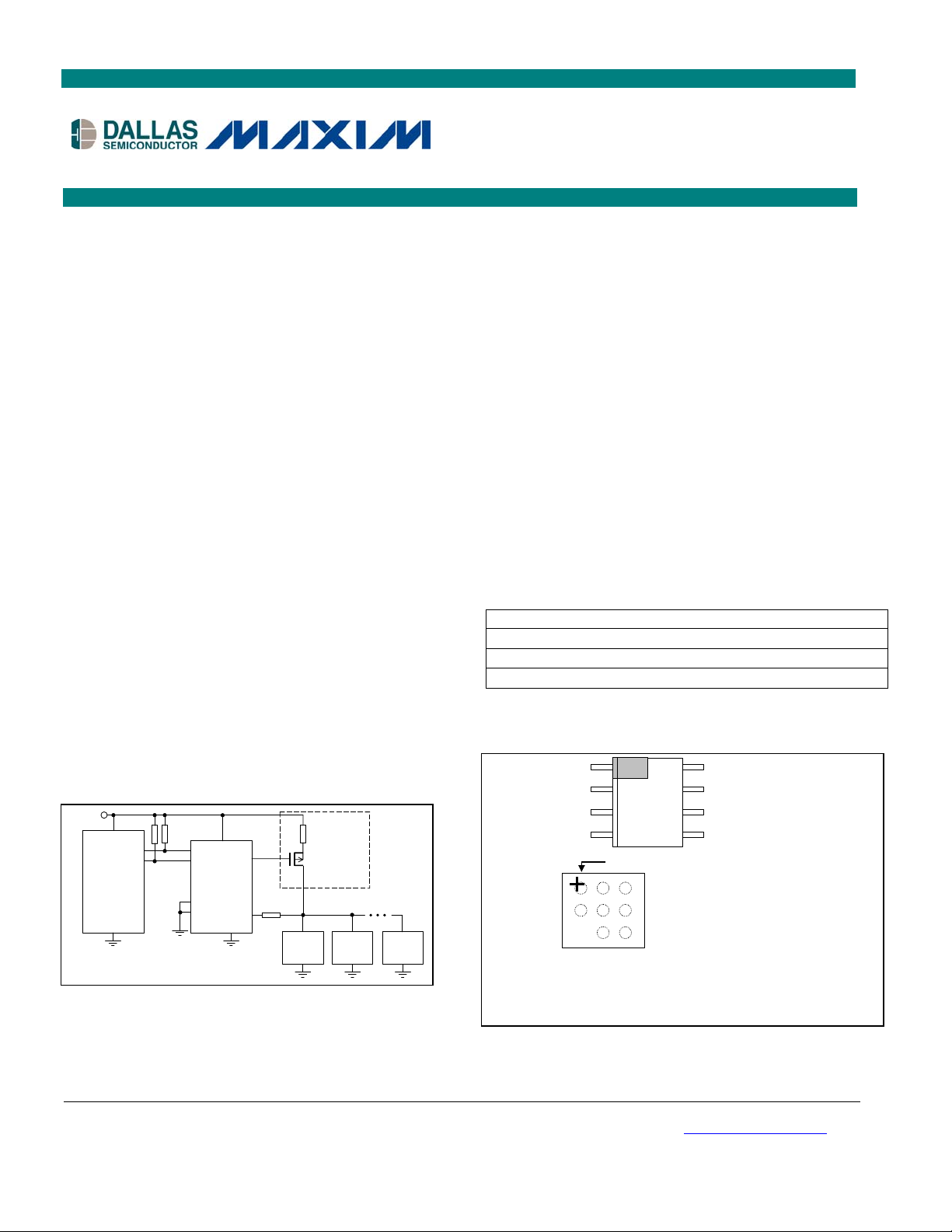
TYPICAL OPERATING CIRCUIT
V
CC
(I²C port)
µC
1-Wire is a registered trademark of Maxim Integrated Products, Inc.
*RP
SDA
SCL
DS2482-100
AD0
AD1
PCTLZ
IO
Current Limiting
Resistor
Optional
circuitry
1-Wire line
*Rt
1-Wire
Device
1-Wire
Device
1-Wire
Device
DS2482-100
Single-Channel 1-Wire Maste
FEATURES
I2C Host Interface, Supports 100kHz and 400kHz
2
C Communication Speeds
I
1-Wire Master IO with Selectable Active or
Passive 1-Wire Pullup
Provides Reset/Presence, 8-Bit, Single-Bit, and
Three-Bit 1-Wire IO Sequences
Standard and Overdrive 1-Wire Communication
Speeds
Slew Controlled 1-Wire Edges
Selectable 1-Wire Slave Presence-Pulse Falling
Edge Masking to Control Fast Edges on the
1-Wire Line
Strong 1-Wire Pullup Provided by an Internal
Low-Impedance Signal Path
PCTLZ Output to Optionally Control an External
MOSFET for Stronger Pullup Requirements
Two Address Inputs for I
Operating Range: 2.9V to 5.5V, -40°C to +85°C
8-Pin, 150-mil SO Package and 9 WLP Package
ORDERING INFORMATION
PART TEMP RANGE PIN-PACKAGE
DS2482S-100+
DS2482S-100+T&R
DS2482X-100+T
+Denotes a lead-free/RoHS-compliant package.
T/T&R = Tape and reel.
PIN CONFIGURATIONS
VCC
IO
GND
SCL
B
C
WLP, Top View with Laser
Mark, Contacts Not Visible.
See 21-0067 for WLP package outline drawing.
1
2
3
4
1 Mark
4821
yywwrr
##xx
1 2 3
2
C Address Assignment
-40°C to +85°C
-40°C to +85°C
-40°C to +85°C
8
7
6
5
D0
D1
PCTLZ
SDA
1 = PCTLZ
2 = AD1
3 = AD0
B1 = SCL
B2 = SDA
B3 = VCC
C2 = GND
C3 = IO
yywwrr = Date/Revision
###xx = Lot Number
8 SO (150 mils)
8 SO (150 mils)
9 WLP (2.5k pcs)
Note: Some revisions of this device may incorporate deviations from published specifications known as errata. Multiple revisions of any device
may be simultaneously available through various sales channels. For information about device errata, click here: www.maxim-ic.com/errata
.
1 of 22
REV: 061208
Page 2
DS2482-100: Single-Channel 1-Wire Master
ABSOLUTE MAXIMUM RATINGS
Voltage Range on Any Pin Relative to Ground -0.5V, +6V
Maximum Current into Any Pin
Operating Temperature Range
Junction Temperature
+150°C
Storage Temperature Range
Soldering Temperature
Stresses beyond those listed under “Absolute Maximum Ratings” may cause permanent damage to the device. These are stress ratings only,
and functional operation of the device at these or any other conditions beyond those indicated in the operational sections of the specifications is
not implied. Exposure to the absolute maximum rating conditions for extended periods may affect device.
Refer to the IPC/JEDEC J-STD-020 Specification.
±20mA
-40°C to +85°C
-55°C to +125°C
ELECTRICAL CHARACTERISTICS
(VCC = 2.9V to 5.5V, TA = -40°C to +85°C.)
PARAMETER SYMBOL CONDITIONS MIN TYP MAX UNITS
Supply Voltage VCC
Operating Current ICC (Note 1) 0.75 mA
1-Wire Input High V
1-Wire Input Low V
1-Wire Weak Pullup Resistor R
1-Wire Output Low V
Active Pullup On Time t
Strong Pullup Voltage Drop ΔV
Pulldown Slew Rate
(Note 6)
Pullup Slew Rate
(Note 6)
Power-On Reset Trip Point V
WPU
APUOT
STRPU
PD
PU
POR
IH1
IL1
OL1
SRC
SRC
1-Wire TIMING (Note 5) (See Figures 3, 5, 6, and 7)
Write 1/Read Low Time t
Read Sample Time t
1-Wire Time Slot t
Fall Time High-to-Low
(Notes 6, 7)
W1L
MSR
SLOT
t
F1
3.3V 2.9 3.3 3.7
5V 4.5 5.0 5.5
3.3V (Notes 2, 3) 1.9
5V (Notes 2, 3) 3.4
3.3V (Notes 2, 3) 0.9
5V (Notes 2, 3) 1.2
V
V
V
(Note 4) 1000 1675 Ω
At 4mA load 0.4 V
Standard (Notes 4, 5) 2.3 2.5 2.7
Overdrive (Notes 4, 5) 0.4 0.5 0.6
VCC ≥ 3.2V, 1.5mA load
VCC ≥ 5.2V, 3mA load
Standard (3.3V ±10%)
Overdrive (3.3V ±10%)
Standard (5.0V ±10%)
Overdrive (5.0V ±10%)
Standard (3.3V ±10%)
Overdrive (3.3V ±10%)
Standard (5.0V ±10%)
Overdrive (5.0V ±10%)
0.3
0.5
1 4.2
5 22.1
2 6.5
10 40
0.8 4
2.7 20
1.3 6
3.4 31
µs
V
V/µs
V/µs
2.2 V
Standard 7.6 8 8.4
Overdrive 0.9 1 1.1
Standard 13.3 14 15
Overdrive 1.4 1.5 1.8
Standard 65.8 69.3 72.8
Overdrive 9.9 10.5 11.0
µs
µs
µs
Standard (3.3V to 0V) 0.54 3.0
Overdrive (3.3V to 0V) 0.10 0.59
Standard (5.0V to 0V) 0.55 2.2
µs
Overdrive (5.0V to 0V) 0.09 0.44
2 of 22
Page 3
DS2482-100: Single-Channel 1-Wire Master
PARAMETER SYMBOL CONDITIONS MIN TYP MAX UNITS
Write-0 Low Time t
Write-0 Recovery Time t
Reset Low Time t
Presence Detect Sample Time t
Sampling for Short and
Interrupt
Reset High Time t
Presence-Pulse Mask START t
Presence-Pulse Mask STOP t
W0L
REC0
RSTL
MSP
t
SI
RSTH
PPM1
PPM2
Standard 60 64 68
Overdrive 7.1 7.5 7.9
Standard 5.0 5.3 5.6
Overdrive 2.8 3.0 3.2
Standard 570 600 630
Overdrive 68.4 72 75.6
Standard 66.5 70 73.5
Overdrive 7.1 7.5 7.9
Standard 7.6 8 8.4
Overdrive 0.7 0.75 0.8
Standard 554.8 584 613.2
Overdrive 70.3 74 77.7
µs
µs
µs
µs
µs
µs
(Note 8) 9.5 10 10.5 µs
(Note 8) 57 60 63 µs
CONTROL PIN (PCTLZ)
V
= 2.9V, 1.2mA load
Output-Low Voltage V
Output-High Voltage V
OLP
0.4mA load current
OHP
CC
current
0.4 V
V
–
CC
0.5V
V
I²C PINS (Note 9) (See Figure 10)
VCC = 2.9V to 3.7V
LOW Level Input Voltage VIL
= 4.5V to 5.5V
V
CC
HIGH Level Input Voltage VIH
Hysteresis of Schmitt Trigger
Inputs
LOW Level Output Voltage at
3mA Sink Current
Output Fall Time from V
with a Bus Capacitance
V
ILmax
Ihmin
to
V
HYS
0.4 V
V
OL
t
60 250 ns
OF
-0.5
0.7 ×
V
CC
0.05 ×
V
CC
V
0.25 ×
V
CC
0.22 ×
V
CC
V
+
CC
0.5V
V
V
from 10pF to 400pF
Pulse Width of Spikes that are
Suppressed by the Input Filter
SDA and SCL pins only 50 ns
t
SP
Input Current Each I/O Pin with
I
an Input Voltage Between
CCMAX
and 0.9V
CCMAX
0.1V
(Notes 10, 11) -10 10 µA
I
Input Capacitance CI (Note 10) 10 pF
SCL Clock Frequency f
0 400 kHz
SCL
Hold Time (Repeated) START
Condition. After this Period, the
0.6 µs
t
HD:STA
First Clock Pulse is Generated
LOW Period of the SCL Clock t
HIGH Period of the SCL Clock t
Setup Time for a Repeated
START Condition
1.3 µs
LOW
0.6 µs
HIGH
0.6 µs
t
SU:STA
3 of 22
Page 4
DS2482-100: Single-Channel 1-Wire Master
PARAMETER SYMBOL CONDITIONS MIN TYP MAX UNITS
Data Hold Time t
Data Setup Time t
Setup Time for STOP
Condition
Bus Free Time Between a
STOP and START Condition
Capacitive Load for Each Bus
Line
Oscillator Warm-Up Time t
Note 1: Operating current with 1-Wire write byte sequence followed by continuous Read of Status register at 400kHz in Overdrive.
Note 2: With standard speed the total capacitive load of the 1-Wire bus should not exceed 1nF, otherwise the passive pullup on
Note 3: Active pullup guaranteed to turn on between V
Note 4: Active or resistive pullup choice is configurable.
Note 5: Except for t
Note 6: These values apply at full load, i.e., 1nF at standard speed and 0.3nF at Overdrive speed. For reduced load, the pulldown slew
Note 7: Fall time high-to-low (t
Note 8: Presence-pulse masking only applies to standard speed.
Note 9: All I²C timing values are referred to V
Note 10: Applies to SDA, SCL, and AD0, AD1.
Note 11: The I/O pins of the DS2482-100 do not obstruct the SDA and SCL lines if V
Note 12: The DS2482-100 provides a hold time of at least 300ns for the SDA signal (referred to the V
Note 13: The maximum t
Note 14:
Note 15: C
Note 16: I²C communication should not take place for the max t
threshold V
exceed 300pF.
parameters is found to be off the typical value, it is safe to assume that all of these parameters deviate from their typical value in
the same direction and by the same degree.
rate is slightly faster.
undefined region of the falling edge of SCL.
A fast-mode I²C-bus device can be used in a standard-mode I²C-bus system, but the requirement t
met. This is automatically the case if the device does not stretch the LOW period of the SCL signal. If such a device does stretch
the LOW period of the SCL signal, it must output the next data bit to the SDA line tr max + t
(according to the standard-mode I²C-bus specification) before the SCL line is released.
= total capacitance of one bus line in pF. If mixed with HS-mode devices, faster fall times according to I²C-bus Specification
B
v2.1 are allowed.
may not be reached in the available time. With Overdrive speed the capacitive load on the 1-Wire bus must not
IL1
, all 1-Wire timing specifications and t
F1
) is derived from PD
F1
has only to be met if the device does not stretch the LOW period (t
HD:DAT
(Notes 12, 13) 0.9 µs
HD:DAT
(Note 14) 250 ns
SU:DAT
0.6 µs
t
SU:STO
1.3 µs
t
BUF
(Note 15) 400 pF
C
B
(Note 16) 100 µs
OSCWUP
IHmin
and V
IL1MAX
APUOT
, referenced from 0.9 × VCC to 0.1 × VCC.
SRC
and V
ILmax
levels.
OSCWUP
.
IH1MIN
are derived from the same timing circuit. Therefore, if one of these
is switched off.
CC
time following a power-on reset.
of the SCL signal) to bridge the
IHmin
) of the SCL signal.
LOW
SU:DAT
≥250ns must then be
SU:DAT
= 1000 + 250 = 1250ns
PIN DESCRIPTION
PIN NAME FUNCTION
1 VCC Power Supply Input
2 IO IO Driver for 1-Wire Line
3 GND Ground Reference
4 SCL I²C Serial Clock Input. Must be tied to VCC through a pullup resistor.
5 SDA I²C Serial Data Input/Output. Must be tied to VCC through a pullup resistor.
Active-low control output for an external P-channel MOSFET to provide extra power to
6 PCTLZ
7 AD1
8
AD0
the 1-Wire line, e.g., for use with 1-Wire devices that require a higher current temporarily
to operate.
I²C Address Inputs. Must be tied to V
or GND. These inputs determine the I²C slave
CC
address of the device (see Figure 9).
4 of 22
Page 5
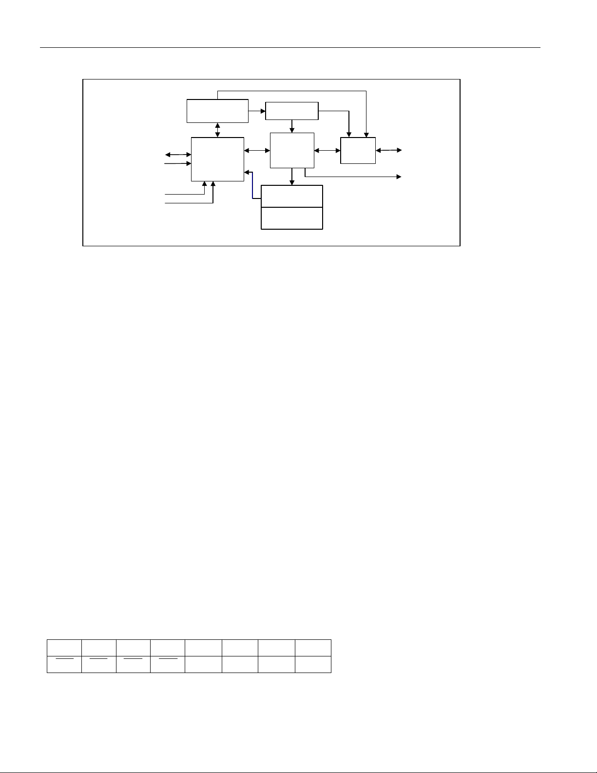
Figure 1. Block Diagram
A
A
DS2482-100
Config
Register
DS2482-100: Single-Channel 1-Wire Master
T-Time OSC
SDA
SCL
D0
D1
I²C
Interface
Controller
I/O
Controller
Status
Register
Read Data
Register
Line
XCVR
IO
PCTLZ
DETAILED DESCRIPTION
The DS2482-100 is a self-timed 1-Wire master, which supports advanced 1-Wire waveform features including
standard and Overdrive speeds, active pullup, strong pullup for power delivery, and presence-pulse masking. The
active pullup affects rising edges on the 1-Wire side. The strong pullup function uses the same pullup transistor as
the active pullup but with a different control algorithm. In addition, the strong pullup activates the PCTLZ pin,
controlling optional external circuitry to deliver additional power beyond the capabilities of the on-chip pullup
transistor. Once supplied with command and data, the I/O controller of the DS2482-100 performs time-critical
1-Wire communication functions such as reset/presence detect cycle, read-byte, write-byte, single-bit R/W and
triplet for ROM Search, without requiring interaction with the host processor. The host obtains feedback
(completion of a 1-Wire function, presence pulse, 1-Wire short, search direction taken) through the Status register
and data through the Read Data register. The DS2482-100 communicates with a host processor through its I
bus interface in standard mode or in fast mode. The logic state of two address pins determines the I
2
2
C slave
C
address of the DS2482-100, allowing up to four devices operating on the same bus segment without requiring a
hub.
DEVICE REGISTERS
The DS2482-100 has three registers that the I²C host can read: Configuration, Status, and Read Data. These
registers are addressed by a read pointer. The position of the read pointer, i.e., the register that the host reads in a
subsequent read access, is defined by the instruction that the DS2482-100 executed last. The host has read and
write access to the Configuration register to enable certain 1-Wire features.
Configuration Register
The DS2482-100 supports four 1-Wire features that are enabled or selected through the Configuration register.
These features are:
Active Pullup (APU)
Presence Pulse Masking (PPM)
Strong Pullup (SPU)
1-Wire Speed (1WS)
These features can be selected in any combination. While APU, PPM, and 1WS maintain their state, SPU returns
to its inactive state as soon as the strong pullup has ended.
Configuration Register Bit Assignment
bit 7 bit 6 bit 5 bit 4 bit 3 bit 2 bit 1 bit 0
1WS SPU PPM APU 1WS SPU PPM APU
After a device reset (power-up cycle or initiated by the Device Reset command) the Configuration register reads
00h. When writing to the Configuration register, the new data is accepted only if the upper nibble (bits 7 to 4) is the
one's complement of the lower nibble (bits 3 to 0). When read, the upper nibble is always 0h.
5 of 22
Page 6
DS2482-100: Single-Channel 1-Wire Master
g
A
A
A
Active Pullup (APU)
The APU bit controls whether an active pullup (controlled slew-rate transistor) or a passive pullup (R
used to drive a 1-Wire line from low to high. When APU = 0, active pullup is disabled (resistor mode). Active Pullup
should be selected if the 1-Wire line has a substantial length (several 10m) or if there is a large number (~20 or
more) of devices connected to a 1-Wire line. The active pullup does not apply to the rising edge of a presence
pulse or a recovery after a short on the 1-Wire line.
The circuit that controls rising edges (Figure 2) operates as follows: At t1 the pulldown (from DS2482-100 or 1-Wire
slave) ends. From this point on the 1-Wire bus is pulled high through R
internal to the DS2482-100. VCC and the
WPU
capacitive load of the 1-Wire line determine the slope. In case that active pullup is disabled (APU = 0), the resistive
pullup continues, as represented by the solid line. With active pullup enabled (APU = 1), when at t2 the voltage has
reached a level between V
IL1max
and V
controlled slew rate, as represented by the dashed line. The active pullup continues until t
, the DS2482-100 actively pulls the 1-Wire line high applying a
IH1min
APUOT
From that time on the resistive pullup continues. See the Strong Pullup (SPU) section for a way to keep the pullup
transistor conducting beyond t3.
resistor) is
WPU
is expired at t3.
Figure 2. Rising Edge Pullup
V
CC
ed
PU = 1
t
1
t
APUOT
t
2
t
3
V
IH1MIN
V
IL1MAX
0V
1-Wire bus is
dischar
PU = 0
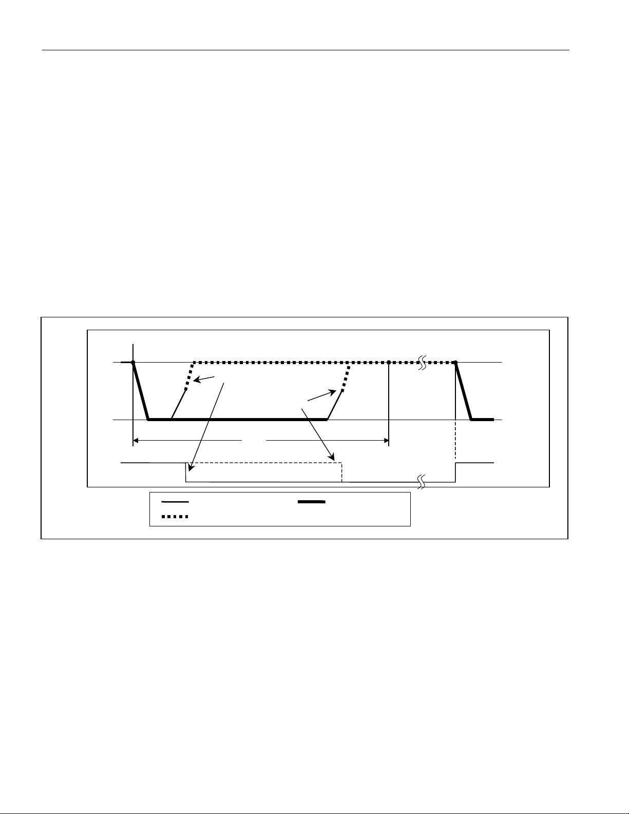
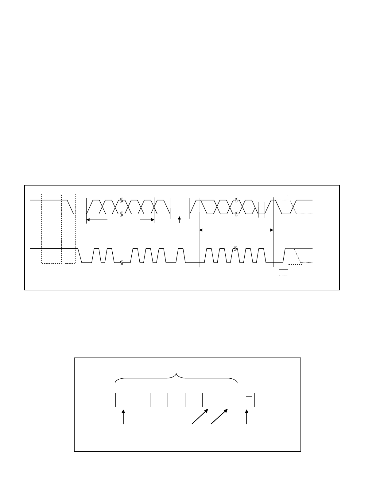
Presence-Pulse Masking (PPM)
The PPM bit controls whether the DS2482-100 masks the leading edge (falling) of presence pulses. When PPM =
0, masking is disabled. Presence pulse masking applies only to standard 1-Wire speed (1WS = 0); this bit has no
function if 1WS = 1 (Overdrive speed). Presence-Pulse Masking can improve the performance of large 1-Wire
networks since it prevents the fast falling edge of a presence pulse generated by a 1-Wire slave device from
propagating through the network and getting reflected. Reflections can cause glitches in the network that in turn
can cause slave devices to lose synchronization with the 1-Wire master.
Figure 3 shows the timing references for the Presence-Pulse Masking. If enabled (PPM = 1), the DS2482-100
begins pulling the 1-Wire line low at t
after the reset low time t
PPM1
is expired. The pulldown ends at t
RSTL
PPM2
, at
which a 1-Wire slave, if present, is pulling the 1-Wire line low. The falling edge of the presence-pulse mask is slewrate controlled.
Figure 3. Presence-Pulse Masking
RESET PULSE PRESENCE PULSE
V
CC
PU con-
0V
trolled edge
t
PPM1
t
t
RSTL
Pull-up DS2482 Pull-down 1-W Slave Pull-down
DS2482 pull-down with PPM = 1; Standard speed only
PPM2
t
Resistive
pull-up
RSTH
6 of 22
Page 7
DS2482-100: Single-Channel 1-Wire Master
Strong Pullup (SPU)
The SPU bit is used to activate the strong pullup function prior to a 1-Wire Write Byte or 1-Wire Single Bit
command. Strong pullup is commonly used with 1-Wire EEPROM devices when copying scratchpad data to the
main memory or when performing an SHA-1 computation, and with parasitically powered temperature sensors or
A/D converters. The respective device data sheets specify the location in the communications protocol after which
the strong pullup should be applied. The SPU bit must be set immediately prior to issuing the command that puts
the 1-Wire device into the state where it needs the extra power. The strong pullup uses the same internal pullup
transistor as the active pullup feature. For cases where the internal strong pullup has insufficient strength, the
PCTLZ pin can be used to control an external p-channel MOSFET to supply additional power beyond the drive
capability of the DS2482-100 to the 1-Wire line. See the ΔV
parameter in the Electrical Characteristics to
STRPU
determine if the internal strong pullup is sufficient given the current load on the device.
If SPU is 1, the DS2482-100 treats the rising edge of the time slot in which the strong pullup starts as if the active
pullup was activated. However, in contrast to the active pullup, the strong pullup, i.e., the internal pullup transistor,
remains conducting, as shown in Figure 4, until one of three events occurs: the DS2482-100 receives a command
that generates 1-Wire communication (the typical case); the SPU bit in the Configuration register is written to 0; or
the DS2482-100 receives the Device Reset command. As long as the strong pullup is active, the PCTLZ output is
low. When the strong pullup ends, the SPU bit is automatically reset to 0. Using the strong pullup feature does not
change the state of the APU bit in the Configuration register.
Figure 4. Low-Impedance Pullup Timing
V
cc
Last bit of 1-Wire Write Byte or 1-Wire Single Bit Function
Write 1 case
Write 0 case
Next
Time Slot
or 1-Wire
Reset
0V
t
SLOT
PCTLZ
DS2482 resistive Pullup DS2482 Pulldown
DS2482 strong Pullup
1-Wire Speed (1WS)
The 1WS bit determines the timing of any 1-Wire communication generated by the DS2482-100. All 1-Wire slave
devices support standard speed (1WS = 0), where the transfer of a single bit (t
65µs. Many 1-Wire device can also communicate at a higher data rate, called Overdrive speed. To change from
standard to Overdrive speed, a 1-Wire device needs to receive an Overdrive Skip ROM or Overdrive Match ROM
command, as explained in the device data sheets. The change in speed occurs immediately after the 1-Wire device
has received the speed-changing command code. The DS2482-100 must take part in this speed change to stay
synchronized. This is accomplished by writing to the Configuration register with the 1WS bit being 1 immediately
after the 1-Wire Byte command that changes the speed of a 1-Wire device. Writing to the Configuration register
with the 1WS bit being 0 followed by a 1-Wire Reset command changes the DS2482-100 and any 1-Wire devices
on the active 1-Wire line back to standard speed.
in Figure 4) is completed within
SLOT
7 of 22
Page 8

DS2482-100: Single-Channel 1-Wire Master
Status Register
The read-only Status register is the general means for the DS2482-100 to report bit-type data from the 1-Wire side,
1-Wire busy status and its own reset status to the host processor. All 1-Wire communication commands and the
Device Reset command position the read pointer at the Status register for the host processor to read with minimal
protocol overhead. Status information is updated during the execution of certain commands only. Details are given
in the description of the various status bits below.
Status Register Bit Assignment
bit 7 bit 6 bit 5 bit 4 bit 3 bit 2 bit 1 bit 0
DIR TSB SBR RST LL SD PPD 1WB
1-Wire Busy (1WB)
The 1WB bit reports to the host processor whether the 1-Wire line is busy. During 1-Wire communication 1WB is 1;
once the command is completed, 1WB returns to its default 0. Details on when 1WB changes state and for how
long it remains at 1 are found in the Function Commands section.
Presence-Pulse Detect (PPD)
The PPD bit is updated with every 1-Wire Reset command. If the DS2482-100 detects a presence pulse from a 1Wire device at t
there is no presence pulse or if the 1-Wire line is shorted during a subsequent 1-Wire Reset command.
Short Detected (SD)
The SD bit is updated with every 1-Wire Reset command. If the DS2482-100 detects a logic 0 on the 1-Wire line at
during the Presence Detect cycle, the SD bit is set to 1. This bit returns to its default 0 with a subsequent 1-Wire
t
SI
Reset command provided that the short has been removed. If SD is 1, PPD is 0. The DS2482-100 cannot
distinguish between a short and a DS1994 or DS2404 signaling a 1-Wire interrupt. For this reason, if a
DS2404/DS1994 is used in the application, the interrupt function must be disabled. The interrupt signaling is
explained in the respective device data sheets.
Logic Level (LL)
The LL bit reports the logic state of the active 1-Wire line without initiating any 1-Wire communication. The 1-Wire
line is sampled for this purpose every time the Status register is read. The sampling and updating of the LL bit
takes place when the host processor has addressed the DS2482-100 in read mode (during the acknowledge
cycle), provided that the Read Pointer is positioned at the Status register.
Device Reset (RST)
If the RST bit is 1, the DS2482-100 has performed an internal reset cycle, either caused by a power-on reset or
from executing the Device Reset command. The RST bit is cleared automatically when the DS2482-100 executes
a Write Configuration command to restore the selection of the desired 1-Wire features.
Single Bit Result (SBR)
The SBR bit reports the logic state of the active 1-Wire line sampled at t
first bit of a 1-Wire Triplet command. The power-on default of SBR is 0. If the 1-Wire Single Bit command sends a
0-bit, SBR should be 0. With a 1-Wire Triplet command, SBR could be 0 as well as 1, depending on the response
of the 1-Wire devices connected. The same result applies to a 1-Wire Single Bit command that sends a 1-bit.
Triplet Second Bit (TSB)
The TSB bit reports the logic state of the active 1-Wire line sampled at t
command. The power-on default of TSB is 0. This bit is updated only with a 1-Wire Triplet command and has no
function with other commands.
Branch Direction Taken (DIR)
Whenever a 1-Write Triplet command is executed, this bit reports to the host processor the search direction that
was chosen by the third bit of the triplet. The power-on default of DIR is 0. This bit is updated only with a 1-Wire
Triplet command and has no function with other commands. For additional information, see the description of the
1-Wire Triplet command and Application Note 187: 1-Wire Search Algorithm.
during the Presence Detect cycle, the PPD bit will be set to 1. This bit returns to its default 0 if
MSP
of a 1-Wire Single Bit command or the
MSR
of the second bit of a 1-Wire Triplet
MSR
8 of 22
Page 9

DS2482-100: Single-Channel 1-Wire Master
FUNCTION COMMANDS
The DS2482-100 understands eight function commands, which fall into four categories: device control, I2C
communication, 1-Wire setup, and 1-Wire communication. The feedback path to the host is controlled by a read
pointer, which is set automatically by each function command for the host to efficiently access relevant information.
The host processor sends these commands and applicable parameters as strings of one or two bytes using the I
interface. The I
or not be acknowledged to indicate an error condition (invalid code or parameter) or to end the communication.
Details of the I
2
C protocol requires that each byte be acknowledged by the receiving party to confirm acceptance
2
C protocol including acknowledge are found in the I2C Interface section.
2
C
Device Reset
Command Code
Command Parameter
Description
Typical Use
Restriction
Error Response
Command Duration
1-Wire Activity
Read Pointer Position
Status Bits Affected
Configuration Bits Affected
F0h
None
Performs a global reset of device state machine logic.
Terminates any ongoing 1-Wire communication.
Device initialization after power-up; re-initialization (reset) as desired.
None (can be executed at any time)
None
Maximum 525ns, counted from falling SCL edge of the command code
acknowledge bit.
Ends maximum 262.5ns after the falling SCL edge of the command code
acknowledge bit.
Status register (for busy polling)
RST set to 1,
1WB, PPD, SD, SBR, TSB, DIR set to 0
1WS, APU, PPM, SPU set to 0
Set Read Pointer
Command Code
Command Parameter
Description
Typical Use
Restriction
Error Response
Command Duration
1-Wire Activity
Read Pointer Position
Status Bits Affected
Configuration Bits Affected
Valid Pointer Codes
E1h
Pointer Code
Sets the Read Pointer to the specified register. Overwrites the read
pointer position of any 1-Wire communication command in progress.
To prepare reading the result from a 1-Wire Byte command; random read
access of registers.
None (can be executed at any time)
If the pointer code is not valid, the pointer code is not acknowledged and
the command is ignored.
None; the read pointer is updated on the rising SCL edge of the pointer
code acknowledge bit.
Not affected
As specified by the pointer code
None
None
Register Selection Code
Status Register F0h
Read Data Register E1h
Configuration Register C3h
9 of 22
Page 10

Write Configuration
Command Code
Command Parameter
Description
Typical Use
Restriction
Error Response
Command Duration
1-Wire Activity
Read Pointer Position
Status Bits Affected
Configuration Bits Affected
1-Wire Reset
Command Code
Command Parameter
Description
Typical Use
Restriction
Error Response
Command Duration
1-Wire Activity
Read Pointer Position
Status Bits Affected
Configuration Bits Affected
DS2482-100: Single-Channel 1-Wire Master
D2h
Configuration Byte
Writes a new configuration byte. The new settings take effect immediately.
NOTE: When writing to the Configuration register, the new data is
accepted only if the upper nibble (bits 7 to 4) is the one's complement of
the lower nibble (bits 3 to 0). When read, the upper nibble is always 0h.
Defining the features for subsequent 1-Wire communication.
1-Wire activity must have ended before the DS2482-100 can process this
command.
Command code and parameter are not acknowledged if 1WB = 1 at the
time the command code is received and the command is ignored.
None; the Configuration register is updated on the rising SCL edge of the
configuration byte acknowledge bit.
None
Configuration register (to verify write)
RST set to 0
1WS, SPU, PPM, APU updated
B4h
None
Generates a 1-Wire Reset/Presence Detect cycle (Figure 5) at the 1-Wire
line. The state of the 1-Wire line is sampled at t
and t
SI
and the result is
MSP
reported to the host processor through the Status register, bits PPD and
SD.
To initiate or end any 1-Wire communication sequence.
1-Wire activity must have ended before the DS2482-100 can process this
command.
Command code is not acknowledged if 1WB = 1 at the time the command
code is received and the command is ignored.
t
RSTL
+ t
+ maximum 262.5ns, counted from the falling SCL edge of the
RSTH
command code acknowledge bit.
Begins maximum 262.5ns after the falling SCL edge of the command
code acknowledge bit.
Status register (for busy polling)
1WB (set to 1 for t
PPD is updated at t
SD is updated at t
RSTL
RSTL
RSTL
+ t
RSTH
+ t
+ tSI
MSP
),
,
1WS, PPM, APU apply
10 of 22
Page 11
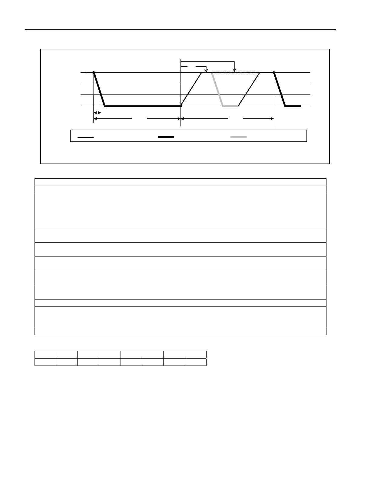
Figure 5. 1-Wire Reset/Presence Detect Cycle
RESET PULSE PRESENCE/SHORT DETECT
V
CC
V
IH1
V
IL1
0V
t
F1
t
RSTL
Pull-up DS2482 pull-down 1-W Slave pull down
DS2482-100: Single-Channel 1-Wire Master
t
t
RSTH
MSP
t
SI
For presence pulse masking and pull-up details see Figure 3.
1-Wire Single Bit
Command Code
Command Parameter
Description
Typical Use
Restriction
Error Response
Command Duration
1-Wire Activity
Read Pointer Position
Status Bits Affected
Configuration Bits Affected
Bit Allocation in the Bit Byte
bit 7 bit 6 bit 5 bit 4 bit 3 bit 2 bit 1 bit 0
V x x x x x x x
x = don’t care
87h
Bit Byte
Generates a single 1-Wire time slot with a bit value ‘V’ as specified by the
bit byte at the 1-Wire line. A ‘V’ value of 0b generates a write-zero time
slot (Figure 6), a value of 1b generates a write-one slot, which also
functions as a read-data time slot (Figure 7). In either case the logic level
at the 1-Wire line is tested at t
To perform single bit writes or reads at the 1-Wire line when single bit
communication is necessary (the exception).
1-Wire activity must have ended before the DS2482-100 can process this
command.
Command code and bit byte are not acknowledged if 1WB = 1 at the time
the command code is received and the command is ignored.
t
+ maximum 262.5ns, counted from the falling SCL edge of the first
SLOT
bit (MS bit) of the bit byte.
Begins maximum 262.5ns after the falling SCL edge of the MS bit of the
bit byte.
Status register (for busy polling and data reading)
1WB (set to 1 for t
SLOT
SBR is updated at t
DIR (may change its state)
1WS, APU, SPU apply
MSR
and SBR is updated.
MSR
)
11 of 22
Page 12

Figure 6. Write-0 Time Slot
V
cc
V
IH1
V
IL1
t
MSR
t
DS2482-100: Single-Channel 1-Wire Master
W0L
0V
t
F1
t
SLOT
t
REC0
Pull-up (see Fig. 2) DS2482 pull-down
Figure 7. Write-1 and Read-Data Time Slot
t
V
cc
V
IH1
V
IL1
t
W1L
MSR
0V
t
F1
t
SLOT
Pull-up (see Fig. 2) DS2482 pull-down 1-W Slave pull-down
NOTE on Figure 7: Depending on its internal state, a 1-Wire slave device transmits data to its master (e.g., the
DS2482-100). When responding with a 0, a 1-Wire slave starts pulling the line low during t
; its internal timing
W1L
generator determines when this pulldown ends and the voltage starts rising again. When responding with a 1, a
1-Wire slave does not hold the line low at all, and the voltage starts rising as soon as t
data sheets use the term t
instead of t
RL
to describe a Read-Data Time Slot. Technically, tRL and t
W1L
is over. 1-Wire device
W1L
W1L
have
identical specifications and cannot be distinguished from each other.
1-Wire Write Byte
Command Code
Command Parameter
Description
Typical Use
Restriction
Error Response
Command Duration
1-Wire Activity
Read Pointer Position
Status Bits Affected
Configuration Bits Affected
A5h
Data Byte
Writes a single data byte to the 1-Wire line.
To write commands or data to the 1-Wire line; equivalent to executing
eight 1-Wire Single Bit commands, but faster due to less I²C traffic.
1-Wire activity must have ended before the DS2482-100 can process this
command.
Command code and data byte are not acknowledged if 1WB = 1 at the
time the command code is received and the command will be ignored.
8 × t
+ maximum 262.5ns, counted from falling edge of the last bit (LS
SLOT
bit) of the data byte.
Begins maximum 262.5ns after falling SCL edge of the LS bit of the data
byte (i.e., before the data byte acknowledge).
NOTE: The bit order on the I²C bus and the 1-Wire line is different.
(1-Wire: LS-bit first; I
2
C: MS-bit first) Therefore, 1-Wire activity cannot
begin before the DS2482-100 has received the full data byte.
Status register (for busy polling)
1WB (set to 1 for 8 × t
SLOT
)
1WS, SPU, APU apply
12 of 22
Page 13

DS2482-100: Single-Channel 1-Wire Master
1-Wire Read Byte
Command Code
Command Parameter
Description
Typical Use
Restriction
Error Response
Command Duration
1-Wire Activity
Read Pointer Position
Status Bits Affected
Configuration Bits Affected
96h
None
Generates eight read-data time slots on the 1-Wire line and stores result
in the Read Data register.
To read data from the 1-Wire line; equivalent to executing eight 1-Wire
Single Bit commands with V = 1 (write-1 time slot), but faster due to less
2
C traffic.
I
1-Wire activity must have ended before the DS2482-100 can process this
command.
Command code is not acknowledged if 1WB = 1 at the time the command
code is received and the command is ignored.
8 × t
+ maximum 262.5ns, counted from the falling SCL edge of the
SLOT
command code acknowledge bit.
Begins maximum 262.5ns after the falling SCL edge of the command
code acknowledge bit.
Status register (for busy polling)
NOTE: To read the data byte received from the 1-Wire line, issue the Set
Read Pointer command and select the Read Data register. Then access
the DS2482-100 in read mode.
1WB (set to 1 for 8 × t
SLOT
)
1WS, APU apply
1-Wire Triplet
Command Code
Command Parameter
Description
Typical Use
Restriction
Error Response
Command Duration
1-Wire Activity
Read Pointer Position
Status Bits Affected
Configuration Bits Affected
Bit Allocation in the Direction Byte
bit 7 bit 6 bit 5 bit 4 bit 3 bit 2 bit 1 bit 0
V x x x x x x x x = don’t care
78h
Direction Byte
Generates three time slots, two read time slots, and one write time slot at
the 1-Wire line. The type of write time slot depends on the result of the
read time slots and the direction byte.
The direction byte determines the type of write time slot if both read time
slots are 0 (a typical case). In this case the DS2482-100 generates a write
1-time slot if V = 1 and a write-0 time slot if V = 0.
If the read time slots are 0 and 1, there follows a write-0 time slot.
If the read time slots are 1 and 0, there follows a write-1 time slot.
If the read time slots are both 1 (error case), the subsequent write time
slot is a write 1.
To perform a 1-Wire Search ROM sequence; a full sequence requires this
command to be executed 64 times to identify and address one device.
1-Wire activity must have ended before the DS2482-100 can process this
command.
Command code and direction byte is not acknowledged if 1WB = 1 at the
time the command code is received and the command will be ignored.
3 × t
+ maximum 262.5ns, counted from the falling SCL edge of the
SLOT
first bit (MS bit) of the direction byte.
Begins maximum 262.5ns after the falling SCL edge of the MS bit of the
direction byte.
Status register (for busy polling)
1WB (set to 1 for 3 × t
SBR is updated at the first t
SLOT
)
MSR
TSB and DIR are updated at the second t
1WS, APU apply
(i. e., at t
MSR
SLOT
+ t
MSR
)
13 of 22
Page 14
DS2482-100: Single-Channel 1-Wire Master
A
W
A
I2C INTERFACE
General Characteristics
The I²C bus uses a data line (SDA) plus a clock signal (SCL) for communication. Both SDA and SCL are
bidirectional lines, connected to a positive supply voltage through a pullup resistor. When there is no
communication, both lines are HIGH. The output stages of devices connected to the bus must have an open-drain
or open-collector to perform the wired-AND function. Data on the I²C-bus can be transferred at rates of up to
100kbps in the standard mode, up to 400kbps in the fast mode. The DS2482-100 works in both modes.
A device that sends data on the bus is defined as a transmitter, and a device receiving data as a receiver. The
device that controls the communication is called a “master.” The devices that are controlled by the master are
“slaves.” To be individually accessed, each device must have a slave address that does not conflict with other
devices on the bus.
Data transfers may be initiated only when the bus is not busy. The master generates the serial clock (SCL),
controls the bus access, generates the START and STOP conditions, and determines the number of data bytes
transferred between START and STOP (Figure 8). Data is transferred in bytes with the most significant bit being
transmitted first. After each byte follows an acknowledge bit to allow synchronization between master and slave.
Figure 8. I²C Protocol Overview
MS-bit
ACK
R/
bit
ACK
bit
SDA
Slave Address
SCL
Idle
START
Condition
Acknowledgment
1 2 6 7 8
from Receiver
9 91 2 8
CK
Repeated if more bytes
are transferred
CK
STOP Condition
Repeated START
Condition
Slave Address
The slave address to which the DS2482-100 responds is shown in Figure 9. The logic states at the address pins
AD0 and AD1 determine the value of the address bits A0 and A1. The address pins allow the device to respond to
one of four possible slave addresses. The slave address is part of the slave address/control byte. The last bit of the
slave address/control byte (R/W) defines the data direction. When set to a 0, subsequent data flows from master to
slave (write access); when set to a 1, data flows from slave to master (read access).
Figure 9. DS2482-100 Slave Address
A6 A5 A4 A3 A2 A1 A0
7-Bit Slave Address
0 0 1 1 0 AD1 AD0 R/W
Most Significant Bit
AD1, AD0 Pin
States
Determines
Read or Write
14 of 22
Page 15

DS2482-100: Single-Channel 1-Wire Master
I2C Definitions
The following terminology is commonly used to describe I2C data transfers. The timing references are defined in
Figure 10.
Figure 10. I²C Timing Diagram
SDA
t
BUF
t
LOW
SCL
STOP START
t
HD:STA
t
R
NOTE: TIMING IS REFERENCED TO V
t
ILMAX
HD:DAT
AND V
t
F
t
HIGH
IHMIN
.
t
SU:DAT
Repeated
Bus Idle or Not Busy: Both SDA and SCL are inactive and in their logic HIGH states.
START Condition: To initiate communication with a slave, the master must generate a START condition. A
START condition is defined as a change in state of SDA from HIGH to LOW while SCL remains HIGH.
STOP Condition: To end communication with a slave, the master must generate a STOP condition. A STOP
condition is defined as a change in state of SDA from LOW to HIGH while SCL remains HIGH.
Repeated START Condition: Repeated starts are commonly used for read accesses to select a specific data
source or address to read from. The master can use a repeated START condition at the end of a data transfer to
immediately initiate a new data transfer following the current one. A repeated START condition is generated the
same way as a normal START condition, but without leaving the bus idle after a STOP condition.
Data Valid: With the exception of the START and STOP condition, transitions of SDA may occur only during the
LOW state of SCL. The data on SDA must remain valid and unchanged during the entire high pulse of SCL plus
the required setup and hold time (t
after the falling edge of SCL and t
HD:DAT
Figure 10). There is one clock pulse per bit of data. Data is shifted into the receiving device during the rising edge
of SCL.
When finished with writing, the master must release the SDA line for a sufficient amount of setup time (minimum
+ tR in Figure 10) before the next rising edge of SCL to start reading. The slave shifts out each data bit on
t
SU:DAT
SDA at the falling edge of the previous SCL pulse and the data bit is valid at the rising edge of the current SCL
pulse. The master generates all SCL clock pulses, including those needed to read from a slave.
Acknowledge: Usually, a receiving device, when addressed, is obliged to generate an acknowledge after the
receipt of each byte. The master must generate a clock pulse that is associated with this acknowledge bit. A device
that acknowledges must pull SDA LOW during the acknowledge clock pulse in such a way that SDA is stable LOW
during the HIGH period of the acknowledge-related clock pulse plus the required setup and hold time (t
the falling edge of SCL and t
before the rising edge of SCL).
SU:DAT
Not Acknowledged by Slave: A slave device may be unable to receive or transmit data, e.g., because it is busy
performing some real-time function. In this case the slave device does not acknowledge its slave address and
leaves the SDA line HIGH.
START
t
t
SU:STA
HD:STA
t
SP
Spike
Suppression
before the rising edge of SCL, see
SU:DAT
t
SU:STO
HD:DAT
after
15 of 22
Page 16

DS2482-100: Single-Channel 1-Wire Master
A slave device that is ready to communicate acknowledges at least its slave address. However, some time later the
slave may refuse to accept data, e.g., because of an invalid command code or parameter. In this case the slave
device does not acknowledge any of the bytes that it refuses and leaves SDA HIGH. In either case, after a slave
has failed to acknowledge, the master first needs to generate a repeated START condition or a STOP condition
followed by a START condition to begin a new data transfer.
Not Acknowledged by Master: At some time when receiving data, the master must signal an end of data to the
slave device. To achieve this, the master does not acknowledge the last byte that it has received from the slave. In
response, the slave releases SDA, allowing the master to generate the STOP condition.
Writing to the DS2482-100
To write to the DS2482-100, the master must access the device in write mode, i.e., the slave address must be sent
with the direction bit set to 0. The next byte to be sent is a command code, which, depending on the command,
may be followed by a command parameter. The DS2482-100 acknowledges valid command codes and
expected/valid command parameters. Additional bytes or invalid command parameters are never acknowledged.
Reading from the DS2482-100
To read from the DS2482-100, the master must access the device in read mode, i.e., the slave address must be
sent with the direction bit set to 1. The read pointer determines the register that the master will read from. The
master may continue reading the same register over and over again, without having to re-address the device, e.g.,
to watch the 1WB changing from 1 to 0. To read from a different register, the master must issue the Set Read
Pointer command and then access the DS2482-100 again in read mode.
I²C Communication—Legend
SYMBOL DESCRIPTION SYMBOL DESCRIPTION
S START Condition DRST Command "Device Reset", F0h
AD, 0 Select DS2482-100 for Write Access WCFG Command "Write Configuration", D2h
AD, 1 Select DS2482-100 for Read Access SRP Command "Set Read Pointer", E1h
Sr Repeated START Condition 1WRS Command "1-Wire Reset", B4h
P STOP Condition 1WWB Command "1-Wire Write Byte", A5h
A Acknowledged 1WRB Command "1-Wire Read Byte", 96h
A\ Not Acknowledged 1WSB Command "1-Wire Single Bit", 87h
(Idle) Bus Not Busy 1WT Command "1-Wire Triplet", 78h
<byte> Transfer of One Byte
Data Direction Codes
Master-to-Slave Slave-to-Master
16 of 22
Page 17

DS2482-100: Single-Channel 1-Wire Master
I²C Communication Examples
Device Reset, e.g., After Power-Up
S AD,0 A DRST A Sr AD,1 A <byte> A\ P
This example includes an optional read access to verify the success of the command.
Write Configuration, e.g., Before Starting 1-Wire Activity
Case A: 1-Wire Idle (1WB = 0)
S AD,0 A WCFG A <byte> A Sr AD,1 A <byte> A\ P
This example includes an optional read access to verify the success of the command.
Case B: 1-Wire Busy (1WB = 1)
S AD,0 A WCFG A\ P
The master should stop and restart as soon as the DS2482-100 does not acknowledge the command code.
Set Read Pointer, e.g., to Read from Another Register
Case A: Valid Read Pointer Code
S AD,0 A SRP A C3h A P
C3h is the valid read pointer code for the Configuration register.
Case B: Invalid Read Pointer Code
S AD,0 A SRP A E5h A\ P
E5h is an invalid read pointer code.
1-Wire Reset, e.g., to Begin or End 1-Wire Communication
Case A: 1-Wire Idle (1WB = 0), No Busy Polling to Read the Result
S AD,0 A 1WRS A P (Idle) S AD,1 A <byte> A\ P
In the first cycle, the master sends the command; then the master waits (Idle) for the 1-Wire Reset to complete. In
the second cycle the DS2482-100 is accessed to read the result of the 1-Wire Reset from the Status register.
Case B: 1-Wire Idle (1WB = 0), Busy Polling Until the 1-Wire Command is Completed, then Read the Result
S AD,0 A 1WRS A Sr AD,1 A <byte> A <byte> A\ P
Repeat until the 1WB bit has changed to 0.
Case C: 1-Wire Busy (1WB = 1)
S AD,0 A 1WRS A\ P
The master should stop and restart as soon as the DS2482-100 does not acknowledge the command code.
17 of 22
Page 18

DS2482-100: Single-Channel 1-Wire Master
1-Wire Write Byte, e.g., to Send a Command Code to the 1-Wire Line
Case A: 1-Wire idle (1WB = 0), No Busy Polling
S AD,0 A 1WWB A 33h A P (Idle)
33h is the valid 1-Wire ROM function command for Read ROM. The idle time is needed for the 1-Wire function to
complete. There is no data read back from the 1-Wire line with this command.
Case B: 1-Wire Idle (1WB = 0), Busy Polling Until the 1-Wire Command is Completed.
S AD,0 A 1WWB A 33h A
Sr AD,1 A <byte> A <byte> A\ P
When 1WB has changed from 1 to 0, the 1-Wire Write Byte command is completed.
Case C: 1-Wire Busy (1WB = 1)
S AD,0 A 1WWB A\ P
The master should stop and restart as soon as the DS2482-100 does not acknowledge the command code.
1-Wire Read Byte, e.g., to Read a Byte from the 1-Wire Line
Case A: 1-Wire Idle (1WB = 0), No Busy Polling, Set Read Pointer After Idle Time
S AD,0 A 1WRB A P (Idle)
S AD,0 A SRP A E1h A Sr AD,1 A <byte> A\ P
The idle time is needed for the 1-Wire function to complete. Then set the read pointer to the Read Data register
(code E1h) and access the device again to read the data byte that was obtained from the 1-Wire line.
Case B: 1-Wire Idle (1WB = 0), No Busy Polling, Set Read Pointer Before Idle Time
S AD,0 A 1WRB A Sr AD,0 A SRP A E1h A P
(Idle) S AD,1 A <byte> A\ P
The read pointer is set to the Read Data register (code E1h) while the 1-Wire Read Byte command is still in
progress. Then, after the 1-Wire function is completed, the device is accessed to read the data byte that was
obtained from the 1-Wire line.
Case C: 1-Wire Idle (1WB = 0), Busy Polling Until the 1-Wire Command is Completed
S AD,0 A 1WRB A
Sr AD,1 A <byte> A <byte> A\
Sr AD,0 A SRP A E1h A Sr AD,1 A <byte> A\ P
Poll the Status register until the 1WB bit has changed from 1 to 0. Then set the read pointer to the Read Data
register (code E1h) and access the device again to read the data byte that was obtained from the 1-Wire line.
Case D: 1-Wire Busy (1WB = 1)
S AD,0 A 1WRB A\ P
The master should stop and restart as soon as the DS2482-100 does not acknowledge the command code.
Repeat until the 1WB
bit has changed to 0.
Repeat until the 1WB
bit has changed to 0.
18 of 22
Page 19

DS2482-100: Single-Channel 1-Wire Master
1-Wire Single Bit, e.g., to Generate a Single Time Slot on the 1-Wire Line
Case A: 1-Wire Idle (1WB = 0), No Busy Polling
S AD,0 A 1WSB A <byte> A P (Idle)
S AD,1 A <byte> A\ P
The idle time is needed for the 1-Wire function to complete. Then access the device in read mode to get the result
from the 1-Wire single-bit command.
Case B: 1-Wire Idle (1WB = 0), Busy Polling Until the 1-Wire Command is Completed
S AD,0 A 1WSB A <byte> A
Sr AD,1 A <byte> A <byte> A\ P
When 1WB has changed from 1 to 0, the Status register holds the valid result of the 1-Wire Single Bit command.
Case C: 1-Wire Busy (1WB = 1)
S AD,0 A 1WSB A\ P
The master should stop and restart as soon as the DS2482-100 does not acknowledge the command code.
1-Wire Triplet, e.g., to Perform a Search ROM Function on the 1-Wire Line
Repeat until the 1WB
bit has changed to 0.
Case A: 1-Wire Idle (1WB = 0), No Busy Polling
S AD,0 A 1WT A <byte> A P (Idle)
S AD,1 A <byte> A\ P
The idle time is needed for the 1-Wire function to complete. Then access the device in read mode to get the result
from the 1-Wire Triplet command.
Case B: 1-Wire Idle (1WB = 0), Busy Polling Until the 1-Wire Command is Completed
S AD,0 A 1WT A <byte> A
Sr AD,1 A <byte> A <byte> A\ P
When 1WB has changed from 1 to 0, the Status register holds the valid result of the 1-Wire Triplet command.
Case C: 1-Wire Busy (1WB = 1)
S AD,0 A 1WT A\ P
The master should stop and restart as soon as the DS2482-100 does not acknowledge the command code.
Repeat until the 1WB
bit has changed to 0.
19 of 22
Page 20
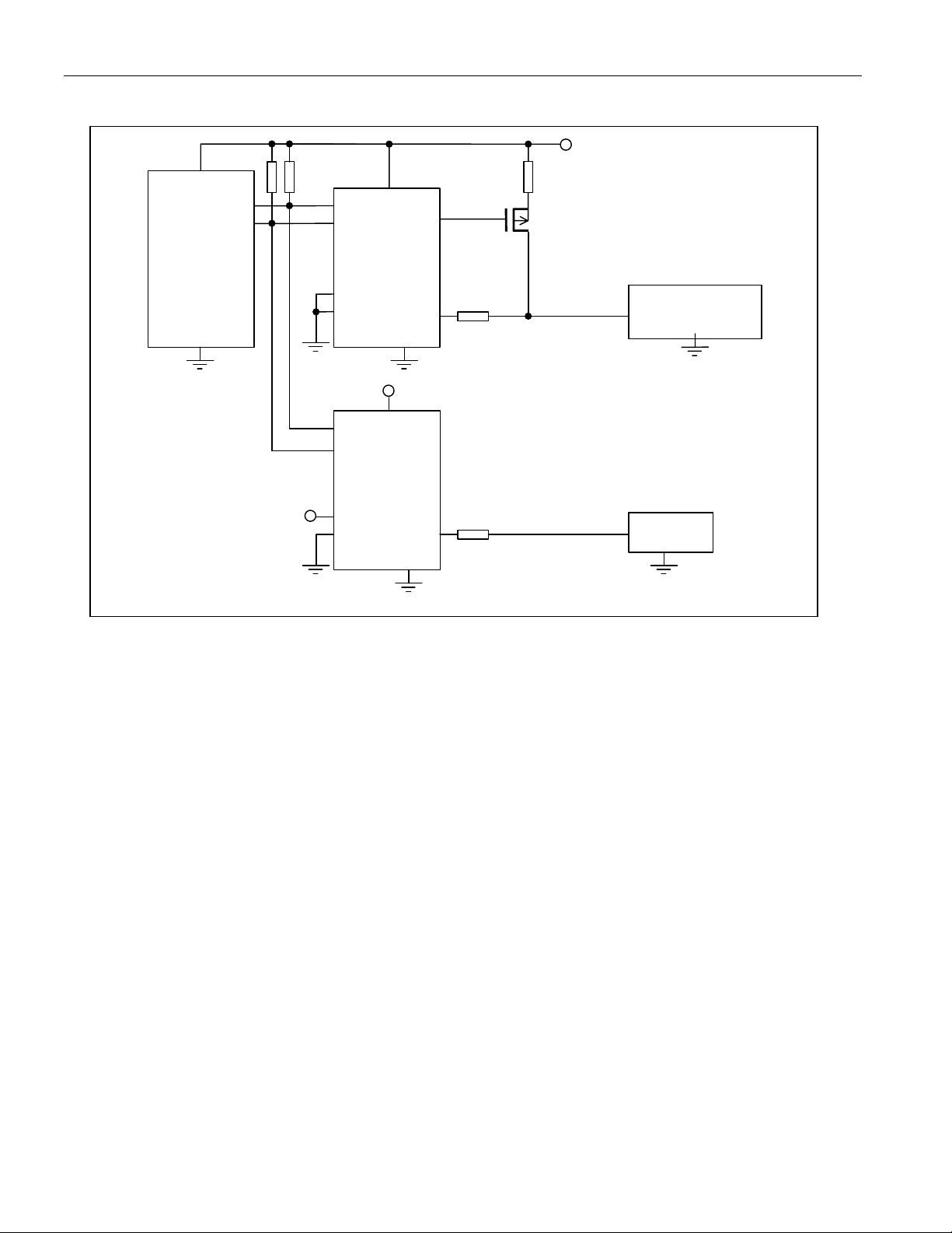
Figure 11. Application Schematic
)
A
A
A
A
*R
P
(I²C port)
SDA
SCL
PCTLZ
DS2482-100: Single-Channel 1-Wire Master
V
CC
Current Limiting
Resistor
µC
DS2482-100
D0
D1
V
CC
SDA
SCL
V
CC
D0
D1
PCTLZ
DS2482-100
IO
IO
*R
t
* Rt Line termination resistor, typically 100
R
P
Information for R
t
1-Wire line
I²C pull-up resistor, see Application
1-Wire line*R
sizing.
P
APPLICATION INFORMATION
SDA and SCL Pullup Resistors
SDA is an open-drain output on the DS2482-100 that requires a pullup resistor to realize high logic levels. Because
the DS2482-100 uses SCL only as input (no clock stretching) the master may drive SCL either through an opendrain/collector output with a pullup resistor or a push-pull output.
Pullup Resistor RP Sizing
According to the I2C specification, a slave device must be able to sink at least 3mA at a VOL of 0.4V. This DC
condition determines the minimum value of the pullup resistor: Rpmin = (V
voltage of 5.5V, the minimum value for the pullup resistor is 1.7kΩ. The "Minimum RP" line in Figure 12 shows how
the minimum pullup resistor changes with the operating voltage.
2
C systems, the rise time and fall time are measured from 30% to 70% of the pullup voltage. The maximum
For I
bus capacitance C
fast speed. Assuming maximum rise time, the maximum resistor value at any given capacitance C
as: Rpmaxs = 1000ns/(C
capacitance of 400pF the maximum pullup resistor values are 2.95kΩ at standard speed and 885Ω at fast speed. A
value between of 1.7kΩ and 2.95kΩ meets all requirements at standard speed.
is 400 pF. The maximum rise time at standard speed must not exceed 1000ns and 300ns at
B
*ln(7/3)) (standard speed) and Rpmaxf = 300ns/(CB*ln(7/3)) (fast speed). For a bus
B
1-Wire Device #1
(with special power
requirements
Ω
1-Wire
Device #2
- 0.4V)/3mA. With an operating
CC
is calculated
B
20 of 22
Page 21

DS2482-100: Single-Channel 1-Wire Master
Since a 885Ω pullup resistor, as would be required to meet the rise time specification at fast speed and 400pF bus
capacitance, is lower than Rpmin at 5.5V, a different approach is necessary. The "Max. Load…" line in Figure 12 is
generated by first calculating the minimum pullup resistor at any given operating voltage ("Minimum Rp" line) and
then calculating the respective bus capacitance that yields a rise time of 300ns.
Only for pullup voltages of 3V and lower can the maximum permissible bus capacitance of 400pF be maintained. A
reduced bus capacitance of 300pF is acceptable for pullup voltages of 4V and lower. For fast speed operation at
any pullup voltage, the bus capacitance must not exceed 200pF. The corresponding pullup resistor value at the
voltage is indicated by the "Minimum Rp" line.
Figure 12. I2C Fast Speed Pullup Resistor Selection Chart
"Minimum Rp" Max. Load at Min. Rp fast mode
2000
1600
1200
800
400
Minimum Rp (Ohms)
0
12345
Pull-up Voltage
PACKAGE INFORMATION
For the latest package outline information and land patterns, go to www.maxim-ic.com/packages.
PACKAGE TYPE PACKAGE TYPE DOCUMENT NO.
8 SO (150 mils) —
9 WLP W92A1+1
500
400
300
200
Load (pF)
100
0
56-G2008-001
21-0067
21 of 22
Page 22

REVISION HISTORY
REVISION
DATE
Updated the Features bullets. 1
Updated the V
061208
Minor corrections to Figure 1; updated the Detailed Description section to
clarify information about the active pullup and strong pullup.
Replaced the Strong Pullup (SPU) section description and replaced Figure 4. 7
Removed timing inaccuracies in Figure 8. 14
and R
IL1
DS2482-100: Single-Channel 1-Wire Master
DESCRIPTION
values in the Electrical Characteristics table. 2
WPU
PAGES
CHANGED
5
22 of 22
Maxim/Dallas Semiconductor cannot assume responsibility for use of any circuitry other than circuitry entirely embodied in a Maxim/Dallas Semiconductor product.
No circuit patent licenses are implied. Maxim/Dallas Semiconductor reserves the right to change the circuitry and specifications without notice at any time.
Maxim Integrated Products, 120 San Gabriel D rive, Sunnyvale, CA 94086 408-737-7600
The Maxim logo is a registered trademark of Maxim Integrated Products, Inc. The Dallas logo is a registered trademark of Dallas Semiconductor Corporation.
© 2008 Maxim Integrated Products
 Loading...