

Page 1
r
www.dalsemi.com
DS2480
Serial 1-Wire™ Line Drive
FEATURES
Universal, common-ground serial port to
1-WireTM line driver for MicroLAN
applications
Works with all iButtons™ and MicroLANcompatible 1-Wire slave devices
Communicates at regular and Overdriv e 1-W ire
speed and serial port data rates of 9600
(default), 19200, 57600 and 115200 bps
Supports 12V EPROM programming and stiff
5V pull-up for Crypto iButton, sensors and
EEPROM
Self-calibrating time base with ±5% tolerance
for serial and 1-Wire communication
Slew rate controlled 1-Wire pull-down and
active pull-up to accommodate long lines and
reduce radiation
User-selectable RXD/TXD polarity minimizes
component count when interfacing to 5V
based RS232 systems or directly to UARTs
Programmable 1-Wire timing and driver
characteristics accommodate a wide range of
MicroLAN configurations at regular speed
Smart protocol combines data and control
information without requiring extra pins
Compatible to optical, IR and RF to RS232
converters
Low cost 8-pin SOIC surface mount package
Operates over 4.5V to 5.5V from -40°C to
+85°C
TM
PIN ASSIGNMENT
1
GND
1-W
NC
V
DD
8-PIN SOIC
(150 MIL)
8
RXD
2
7
TXD
3
4
POL
6
V
PP
5
PIN DESCRIPTION
GND Ground
1-W 1-Wire Input/Output
NC No Connection
V
V
DD
PP
4.5 to 5.5V
Optional EPROM
Programming Voltage
POL RXD/TXD Polarity Select
TXD Serial Data from UART
RXD Serial Data to UART
ORDERING INFORMATION
DS2480S 8-pin SOIC
1 of 33 012501
Page 2
DS2480
DESCRIPTION
The DS2480 is a serial port to 1-Wire interface chip that supports standard and Overdrive speeds. It
connects directly to UARTs and 5V RS232 systems. Interfacing to RS232C (± 12V levels) requires a
passive clamping circuit and one 5V to ± 12V level translator. Internal timers relieve the host of the
burden of generating the time-critical 1-Wire communication waveforms. In contrast to the
DS9097 (E) where a full character must be sent by the host for each 1-W ire time slot, the DS2480 can
translate each character into eight 1-Wire time slots thereby increasing the data throughput
significantly. In addition, the DS2480 can be set to communicate at four different data rates including
115.2 kbps, 57.6 kbps and 19.2 kbps with 9.6 kbps being the power-on default. Command codes
received from the host’s crystal controlled UART serve as a reference to continuously calibrate the onchip timing generator. The DS2480 uses a unique protocol that merges data and control information
without requiring control pins. This approach maintains compatibility to off-the-shelf serial to
wireless converters allowing easy realization of 1-Wire media jumpers. The various control functions
of the DS2480 are optimized for MicroLAN 1-Wire networks and support the special needs of all
current 1-Wire devices including the Crypto iButton, EPROM-based Add-Only Memories, EEPROM
devices and 1-Wire Thermometers.
DETAILED PIN DESCRIPTION
PIN SYMBOL DESCRIPTION
1 GND Ground Pin: common ground reference and ground return for 1-Wire bus
2 1-W 1-Wire Input/Output Pin: 1-Wire bus with slew-rate-controlled pull-down, active
pull-up, ability to switch in VPP to program EPROM, and ability to switch in
VDD through a low-impedance path to program EEPROM, perform a
temperature conversion or operate the Crypto iButton.
3 NC No Connection Pin.
4V
5V
DD
PP
6 POL RXD/TXD Polarity Select: RXD/TXD polarity select; tied to GND for RS232
7 TXD Serial Data from UART: data input from host (inverted or true); maximum
8 RXD Serial Data to UART: signal output to host; push-pull driver with CMOS
Power Input Pin: power supply for the chip and 1-Wire pull-up voltage. 5V ±
10%; may be derived from 12V VPP with an external voltage regulator.
EPROM Programming Voltage: 12V supply input for EPROM programming; if
EPROM programming is not required, this pin must be tied to VDD. VPP must
come up before VDD.
(12V or 5V) connection, tied to V
voltage swing -0.3V to V
+ 0.3V; for logic thresholds see DC specifications.
DD
for direct connection to UART chip.
DD
compatible levels; for true ±12V RS232 systems an external level-translator
must be provided.
2 of 28
Page 3
DS2480
OVERVIEW
The DS2480 directly interfaces a 5-volts serial communication port with its lines TXD (transmit) and
RXD (receive) to a 1-Wire bus. In addition the device performs a sp eed conversion allowin g the data rate
at the communication port to be different from the 1-Wire date rate. Several parameters relating to the
1-Wire port and its timing as well as the communication speed at both the port and the 1-Wire bus are
configurable. The circuit to achieve these functions is outlined in Figure 1, Block Diagram. The device
gets its input data from the serial communication port of the host computer through pin TXD. For
compatibility with active-high as well as active-low systems, the incoming signal can be inverted by
means of the polarity input POL. The polarity chosen by hard wiring the logic level of this pin is also
valid for the output pin RXD. If for minimizing the interface hardware an asymmetry between RXD and
TXD is desired, this can be achieved by setting the most significant bit of the Speed Control parameter to
a 1 (see Configuration Parameter Value Codes). With the MS bit of the speed control set to 1, the polarity
at TXD is still selected by the logic level at POL, but the polarity at RXD will be the opposite of what the
logic level at POL specifies. As data enters the core of the DS2480’s logic circuitry, it is analyzed to
separate data and command bytes and to calibrate the device’s timing generator. The timing generator
controls all speed relations of the communication interface and the 1-Wire bus as well as the waveforms
on the 1-Wire bus. Command bytes either affect the configuration setting or generate certain waveforms
on the 1-Wire bus. Data bytes are simply translated by the protocol converter into the appropriate 1-W ire
activities. Each data byte generates a return byte from the 1-Wire bus that is communicated back to the
host through the RXD pin as soon as the activity on the 1-Wire bus is completed. The 1-Wire driver
shapes the slopes of the 1-Wire wave forms, applies programming pulses or strong pull-up to 5-volts and
reads the 1-Wire bus using a non-TTL threshold to maximize the noise margin for best performance on
large 1-Wire MicroLAN networks.
DS2480 BLOCK DIAGRAM FIGURE 1
MS BIT OF SPEED CONTROL
(1 = RXD IS INVER TE D)
MUX
RXD
CONFIGURATION
REGISTER
POL
TXD
PROTOCOL
PROTOCOL
ANALYZER
ANALYZER
TIMING
GENERATOR
PROTOCOL
CONVERTER
1-WIRE
DRIVER
PP
V
1-W
3 of 28
Page 4
DS2480
DEVICE OPERATION
The DS2480 can be described as a complex state machine with two static and several dynamic states.
Two device-internal flags as well as functions assigned to certain bit positions in the command codes
determine the behavior of the chip, as shown in the state transition diagram (Figure 2). The DS2480
requires and generates a communication protocol of 8 data bits per character, 1 stop bit and no parity. It is
permissible to use two stop bits on the TXD line. However, the DS2480 will only assert a single stop bit
on RXD. When powering up, the DS2480 performs a master reset cycle and enters the
Command Mode, which is one of the two static states. The device now expects to receive one 1-Wire
reset command on the TXD line sent by the host at a data rate of 9600 bits per second (see section
Communication Commands for details). This command byte is required solely for calibration of the
timing generator the DS2480 and is not translated into any activity on the 1-Wire bus. After this first
command byte the device is ready to receive and execute any command as described later in this
document. A master reset cycle can also be generated by means of software. This may be necessary if the
host for any reason has lost synchronization with the device. The DS2480 will perform a master reset
cycle equivalent to the power-on reset if it detects start polarity in place of the stop bit. The host has
several options to generate this condition. These include making the UART generate a break signal,
sending a NULL character at a data rate of 4800 bps and sending any character with parit y enabled and
selecting space polarity for the parity bit. As with the power-on reset, the DS2480 requires a 1-Wire reset
command sent by the host at a data rate of 9600 bps for calibration.
4 of 28
Page 5
STATE TRANSITION DIAGRAM Figure 2
K
X
A
A
A
A
A
A
V
DS2480
E1h
RESET
SOFTWARE
MASTER RESET
110XSS01
N.C.
110XSS01
111T11Q1
PULSE
TX E3h
N.C.
POWER OFF
N.C.
111T11Q1
E3h
CODE = E3h
INACTIVE
POWER
ON
COMMAND MODE
0ZZZVVV1
N.C.
CONFIGURATION
0ZZZVVV1
CHEC
MODE
RRIVAL
N.C.
N.C.
CC. OFF
T
RRIVAL
CODE
101HSS01
SEARCH
101HSS01
CCEL.
100VSSP1
100VSSP1
N.C.
TX BYTE
SINGLE BIT
FUNCTION
POWER OFF
STR. PULL-UP
RMED
DATA MODE
ALL OTHER
CODES
N.C. = UNCONDITIONAL
LEGEND: V BINARY VALUE (TYPE OF WRITE TIME SLOT)
SS 1-WIRE SPEED SELECTION CODE
P IF LOGIC 1, GENERATES STRONG PULL-UP TO 5V IMMEDIATELY FOLLOWING THE TIME SLOT
T TYPE OF PULSE; 0 = STRONG PULL-UP (5V), 1 = PROGRAMMING PULSE (12V)
Q 1 = ARM STRONG PULL-UP AFTER EVERY BYTE; 0 = DISARM
H SEARCH ACCELERATOR CONTROL; 1 = ACCELERATOR ON, 0 = ACCELERATOR OFF
ZZZ CONFIGURATION PARAMETER CODE (WRITE), 000 = READ CONFIGURATION PARAMETER
VVV CONFIGURATION PARAMETER VALUE CODE ( WRITE), CONFIGURATION PARAMETER CODE (READ)
X DON'T CARE
STR. PULL-UP NOT
ACCELERATOR
N.C.
CHECK SEARCH
PERFORM SEARCH
SEQUENCE
CC.ON
GENERATE STRONG
PULL-UP TO 5
N.C.
After the DS2480 has reached the command mode, the host can send commands such as 1-Wire Reset,
Pulse, Configuration, Search Accelerator and Single Bit functions or switch over to the secon d static state
called Data Mode. In data mode the DS2480 simply converts b ytes it receives at the TXD pin into their
equivalent 1-Wire wave forms and reports the results back to the host through the RXD pin. If the Search
Accelerator is on, each byte seen at TXD will generate a 12 -bit sequence on the 1-Wire bus (see section
Search Accelerator for detail s). If the Stron g Pull-up t o 5-volts is enabled (see Pul se command) e ach b yte
on the 1-Wire bus will be followed by a pause of predefined duration where the bus is pulled to 5-volts
via a low impedance transistor in the 1-Wire driver circuit.
5 of 28
Page 6

DS2480
While being in the Data Mode the DS2480 checks each byte received from the host fo r the reserv ed code
that is used to switch back to Command Mode. To be able to write any possible code (including the
reserved one) to the 1-Wire bus, the transition to the Command Mode is as follows: After having received
the code for switching to Command Mode, the device temporaril y enters the Che ck Mode where it waits
for the next byte. If both bytes are the same, the byte is sent once to the 1-Wire bus and the device returns
to the Data Mode. If the second byte is different from the reserved code, it will be ex ecuted as command
and the device finally enters the Command Mode. As a consequence, if the rese rved code that normally
switches to Command Mode is to be written to the 1-Wire bus, this code byte must be sent twice
(duplicated). This detail must be considered carefully when developing software drivers for the DS2480.
After having completed a memory function with a device on the 1-Wire bus it is recommended to issue a
Reset Pulse. This means that the DS2480 has to be switched to Command mode. The host then s ends the
appropriate command code and continues performing other tasks. If during this time a device arrives at
the 1-Wire bus it will generate a presence pulse. The DS2480 will recognize this unsolicited presence
pulse and notify the host by sending a byte such as XXXXXX01b. The Xs represent undefined bit values.
The fact that the host receives the byte unsolicited together with the pattern 01b in the least significant
two bits marks the bus arrival. If the DS2480 is left in Data Mode afte r completing a memory function
command it will not report any bus arrival to the host.
COMMAND CODE OVERVIEW
The DS2480 is controlled by a variety of commands. All command codes are 8 bits long. The most
significant bit of each command code distinguishes between communication and configuration
commands. Configuration commands access the configuration registers. They can write or read any of the
configurable parameters. Communication commands use data of the configuration register in order to
generate activity on the 1-Wire bus and/or (dis) arm the strong pull-up after every byte or (de) activate the
Search Accelerator without generating activity on the 1-Wire bus. Details on the command codes are
included in the State Transition diagram (Figure 2). A full explanation is given in the subsequent sections
Communication Commands and Configuration Commands.
In addition to the command codes explained in the subsequent sections the DS2480 understands the
following reserved command codes:
E1h switch to Data Mode
E3h switch to Command Mode
F1h pulse termination
Except for these reserved commands, the Search Accelerator control and the first byte after power-on
reset or master reset cycle, every legal command byte generates a response byte. The pulse termination
code triggers the response byte of the terminated pulse command. Illegal command bytes do not generate
a command response byte.
Once the device is switched back from Data Mode to Command Mode one must not repeat the E3h
command while the Command Mode is still active.
COMMUNICATION COMMANDS
The DS2480 supports four communication function commands: Reset, Single Bit, Pulse, and Search
Accelerator control. Details on the assignment of each bit of the comm and codes are shown in Table 1.
The corresponding command response bytes are detailed in Table 2. The Reset, Search Accelerator
Control and Single Bit commands include bits to select the 1-Wire communication speed (regular,
flexible regular, Overdrive). Even if a command does not generate activity on the 1-Wire bus, these bits
are latched inside the device and will take effect immediately.
6 of 28
Page 7
DS2480
COMMUNICATION COMMAND CODES TABLE 1
FUNCTION BIT 7 BIT 6 BIT 5 BIT 4 BIT 3, BIT 2 BIT 1 BIT 0
Single Bit 1 0 0 0 = write 0
1 = write 1
Search
Accelerator
Control
Reset 1 1 0 (don’t care) 00 reg. speed
Pulse 1 1 1 0 = 5V strong pull-up
1 0 1 0 = accelerator off
1 = accelerator on
See Text
1 = 12V prog. pulse
00 reg. speed
01 flex. speed
10 OD. speed
11 reg. speed
00 reg. speed
01 flex. speed
10 OD. speed
11 reg. speed
01 flex. speed
10 OD. speed
11 reg. speed
11 pulse See Text 1
See Text 1
01
01
COMMUNICATION COMMAND RESPONSE TABLE 2
FUNCTION BIT 7 BIT 6 BIT 5 BIT 4 BIT 3 BIT 2 BIT 1 BIT 0
Single Bit 1 0 0 same as sent 1-Wire read back,
both bits same value
Reset 1 1 See
Text
Pulse 1 1 1 same as sent undefined
0 1 0 00 = 1-Wire shorted
01 = presence pulse
10 = alarming presence
pulse
11 = no presence pulse
(The Search Accelerator Control command does not generate a response byte.)
RESET
The Reset command must be used to begin all 1-Wire communication. The speed selection included in
the command code immediately takes effect. The response byte includes a code for the rea ction on the
1-Wire bus (bits 0 and 1) and a code for the chip revision (bits 2 to 4). If bit 5 of the response byte reads
‘1’, a programming voltage is present on the V
devices.
pin, indicating that one may try programming EPROM
PP
SINGLE BIT
The Single Bit command is used to generate a single time slot on the 1-Wire bus at the speed indicated by
bits 2 and 3. The type of the time slot (write zero or write one) is determined by the logic value of bit 4. A
read data time slot is identical to the write one time slot. Bits 0 and 1 of the response b yte transmitted b y
the DS2480 at the end of the time slot reveal the value found on the 1-Wire bus when reading.
For a time slot without a subsequent strong pull-up, bit 1 of the command must be set to 0. For a time slot
immediately followed by a strong pull-up bit 1 must be set to 1. As soon as the strong pull-up is over, the
device will send a second response byte, code EFh (read 1) or ECh (read 0), depending on the value
found on the 1-Wire bus when reading. The strong pull-up directly following the single bit is used in
conjunction with the CryptoiButton.
7 of 28
Page 8
DS2480
SEARCH ACCELERATOR CONTROL
The Search Accelerator Control command is used to set or reset the Search Accelerator control flag. Bit 4
of the command code contains the state to which the accelerator control flag is to be set. If the fl ag is set
to a 1 (on) the device translates every byte received in data mode into a 12-bit sequ ence on the 1-Wire
bus. For details on how the Search Accelerator works please refer to the section Search Accelerator
Operation. Before activating the Search Accelerator, one must make sure that the strong pull-up after
every byte is disarmed (see Pulse Command). The Search Accelerator command does not generate a
command response byte.
Although the Search Accelerator Control command itself does not generate any 1-Wire activit y, it can be
used to select the communication speed on the 1-Wire bus. The speed selection (if different from the
previous setting, e.g., from a Reset command) will take effect immediately.
PULSE
The Pulse command serves several functions that are selected by the contents of bit 1 and bit 4 of the
command code. The main functions are generating a strong pull-up to 5-volts and generating 12-volts
programming pulses for EPROM devices (if the 12-volts are available at the VPP pin). The secondary
function of the pulse command is arming and disarming a strong pull-up after every subsequent byte in
data mode. The arm/disarm function is controlled by bit 1 of the command code. Bit 4 determines
whether the device will generate a strong pull-up to 5-volts or a 12-volts programming pulse. The table
below summarizes these options.
BIT 4 BIT 1 FUNCTION
0 0 strong pull-up to 5V and disarm
1 0 12V Programming Pulse and disarm
0 1 strong pull-up to 5V and arm
1 1 12V Programming Pulse and arm
The strong pull-up to 5-volts is required to program EEPROM devices or to operate special function
devices that require a higher current for a limited time after having received a “go and convert”
command. Therefore and because it significantly reduces the ef fective d ata throu ghput on the 1-W ire bus,
the strong pull-up is disarmed most of the time. Although arming or disarming is simultaneously possible
while generating a programming pulse, this is not recommended since it is likely to destroy the DS2480 if
non-EPROM devices are connected to the 1-Wire bus. The duration of the strong pull-up or programming
pulse is determined by configuration parameters and ranges from a few microseconds up to unlimited (see
section Configuration Commands). However, unlimited duration is not allowed in conjunction with
arming the strong-pull-up after every byte. As long as the DS2480 is in Command Mode the host may
terminate a strong pull-up or programming pulse prematurely at any time by sending the command code
F1h. The response byte is generated as soon as the strong pull-up or programming pulse is over (either
because the predefined time has elapsed or due to termination). The response byte mainly returns the
command code as sent by the host, but the two least significant bits are undefined. If the strong pull-up is
armed and the device is in Data Mode, the end of the strong pull-up will be signaled as code F6h if the
most significant bit of the preceding data byte on the 1-Wire bus was a 1 and 76h otherwise. The host will
see this response byte in addition to the response on the data byte sent (see also section Wave Forms later
in this document).
8 of 28
Page 9
DS2480
SEARCH ACCELERATOR INTRODUCTION
The Search Accelerator is a logic block inside the DS2480 that allows usin g the Search ROM function
very efficiently under modern operating systems such as Windows and Windows 95/NT. Without the
DS2480 all 1-Wire port adapters have to involve the computer’s CPU for ever y single time slot or pulse
to be generated on the 1-Wire bus.
Under DOS, accessing peripherals such as the UART or parallel port is very straight forward and
therefore fast. Under Windows the situation is different and it may take several milliseconds or more to
get the first time slot generated on the 1-Wire bus. Every subsequent time slot will be generated in much
less time, since the computer simply sends out (“streams”) a long chain of bytes. This works reasonably
well when reading or writing large blocks of data.
Searching the 1-Wire bus to identify all ROM IDs of the devices connected, however, requires reading
two bits, making a decision and then writing a bit. This procedure is to be repeated 64 times to identify
and address a single device. With the overhead of modern operating systems this fairly simple process
takes a lot of time, reducing the discovery rate of devices on the 1-Wire bus from a typical value of 40 to
50 per second under DOS to less than 10 under Windows. To solve this problem the Search Accelerator
was developed.
The Search Accelerator receives from the host information on the preferred path to chose during the
execution of the Search ROM function as one contiguous chain of bytes and then translates it into the
appropriate time slots on the 1-Wire bus. In addition, the Search Accelerator reports back to the host the
ROM ID of the device actually addressed and the bit positions in which conflicts were found. (If the
ROM ID of one device has a 0 in a bit position where another device has a 1, this is called a “con flict” on
the electrical level and “discrepancy” on the logical level. See the Book of DS19x x iButton Standards for
a more detailed discussion of the Search ROM). This helps the host to select the preferred path for the
next Search ROM activity.
Since the ROM ID of all MicroLAN compatible devices is 64 bits long and a conflict may occur in any of
these bits, the total length of data reported to the host is 128 bits or 16 bytes. To avoid data overrun (if the
CPU sends data faster than it can be processed) the protocol for the Search Accelerator operation was
defined so that one has to send as many bytes as one will receive. This way the CPU sends 16 bytes for
each path and the UART guarantees the correct data timing and frees the CPU for othe r tasks while the
DS2480 performs a Search ROM function.
SE AR CH AC CELER AT OR O P ERAT ION
After the Search Accelerator is activated and the data mode is selected, the host must send 16 bytes to
complete a single Search ROM pass on the 1-Wire bus. These bytes are constructed as follows:
first byte
76543210
r
3
et cetera
16th byte
76543210
r63 x63 r62 x62 r61 x61 r60 x60
x
3
r
2
x
2
r
1
x
1
r
0
9 of 28
x
0
Page 10

DS2480
In this scheme, the index (values from 0 to 63, “n”) designates the position of the bit in the ROM ID of a
MicroLAN compatible device. The character “x” marks bits that act as filler and do not require a specific
value (don’t care bits). The character “r” marks the path to go at that particular bit in case of a conflict
during the execution of the ROM Search.
For each bit position n (values from 0 to 63) the DS2480 will generate three time slots on the 1-W ire bus.
These are referenced as:
b0 for the first time slot (read data)
b1 for the second time slot (read data) and
b2 for the third time slot (write data).
The type of time slot b2 (write 1 or write 0) is determined by the DS2480 as follows:
b2 = rn if conflict (as chosen by the host)
= b0 if no conflict (there is no alternative)
= 1 if error (there is no response)
The response the host will receive during a complete pass through a Search ROM function using the
Search Accelerator consists of 16 bytes as follows:
first byte
76543210
r’
3
d
3
r’
2
d
2
r’
1
d
1
r’
0
d
0
et cetera
16th byte
76543210
r’
63
d
63
r’
62
d
62
r’
61
d
61
r’
60
d
60
As before, the index (values from 0 to 63, “n”) designates the position of the bit in the ROM ID of a
MicroLAN compatible device. The character “d” marks the discrepancy flag in that particular bit
position. The discrepancy flag will be 1 if there is a conflict or no response in that particular bit position
and 0 otherwise. The character “r’ “ marks the actuall y chosen path at that particular bit position. The
chosen path is identical to b2 for the particular bit position of the ROM ID.
To perform a Search ROM sequence one starts with all bits rn being 0s. In case of a bus error, all
subsequent response bits r’n are 1’s until the Search Accelerator is deactivated. Thus, if r’63 and d63 are
both 1, an error has occurred during the search procedure and the last sequence has to be repeated.
Otherwise r’
(n = 0 ... 63) is the ROM code of the device that has been found and addressed.
n
For the next Search ROM sequence one re-uses the previous set rn (n = 0 ... 63) but sets rm to 1 with “m”
being the index number of the highest discrepancy flag that is 1 and sets all ri to 0 with i > m. This
process is repeated until the highest discrepancy occurs in the same bit position for two consecutive
passes.
The table below shows an example for the communication between host and DS2480 to perform one pass
through the Search ROM function using the Se arch Accelerator. After a device has been identified and
addressed, a (not specified here) memory function is executed and finally a reset pulse is generated. This
example assumes that the DS2480 was in Command Mode and that regular 1-Wire speed is used.
10 of 28
Page 11

DS2480
SEARCH ACCELERATOR USAGE EXAMPLE
Action Sequence Host TX Host RX
Generate Reset Pulse C1 C9
Set Data Mode E1 (nothing)
Search ROM command F0 (as sent)
Set Command Mode E3 (nothing)
Search Accelerator On B1 (nothing)
Set Data Mode E1 (nothing)
Send 16 bytes data response
Set Command Mode E3 (nothing)
Search Accelerator Off A1 (nothing)
Set Data Mode E1 (nothing)
Do Memory Function
Set Command Mode E3 (nothing)
Generate Reset Pulse C1 C9
CONFIGURATION COMMANDS
The DS2480 is designed to be configurable for the varying requirements of its application. When the
device powers up and/or performs a master reset cycle, the hard-wired default configuration settings take
effect. These settings will work on a short 1-Wire bus and assume regular 1-Wire communication speed.
To change these default settings and to verify the current settings, the logic of the DS2480 supports
configuration commands. A summary of the available configuration parameters, their default settings at
regular and Overdrive speed and their applicability is shown in Table 3.
Parameters not related to the communication speed on the 1-Wire bus specify the duration of the 12-volts
programming pulse, the duration of the strong pull-up to 5-volts and the baud rate on the interface that
connects the DS2480 to the host. The remaining three parameters are used to modify the 1-Wire
communication wave forms if one selects “Flexible Speed” (see “Communication Commands” for speed
selection).
Flexible speed is implemented to improve the performance of large MicroLAN Networks. This is
accomplished by:
• limiting the slew rate on falling edges (e. g., at the beginning of time slots, to reduce ringing),
• extending the Write 1 low time (allows the current flow through the network to end slowly, to
prevent voltage spikes from inductive kickback),
• delaying the time point when reading a bit from the 1-Wire bus (gives the network more time to
stabilize, to get a higher voltage margin) and
• adding extra recovery time between Write 0 time slots (allows more energy transfer through the
network, to replenish the parasite power supply of the devices on the bus).
The latter two functions are controlled by a single parameter. Taking advantage of flexible speed requires
changing one or more of these parameters from their default values. Otherwise the waveforms will be
identical to those at regular speed.
Each configuration parameter is identified by its 3-bit parameter code and can be programmed for one of
a maximum 8 different values using a 3-bit value code. A matrix of parameter codes and value codes with
the associated physical values in shown in Table 4.
11 of 28
Page 12
DS2480
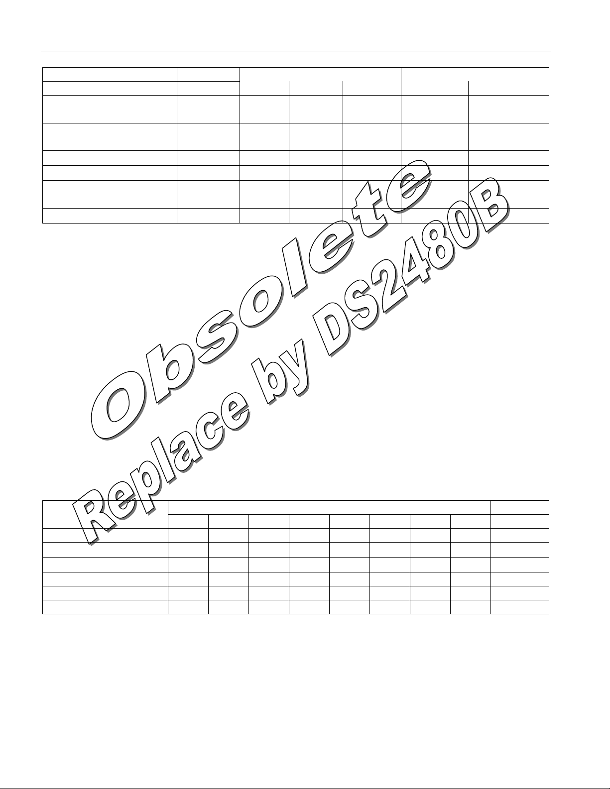
CONFIGURATION COMMAND OVERVIEW TABLE 3
Parameter Description Par. Code Configurable at Default
Regular Flexible Overdrive Reg./Flex. Overdrive
Pull-Down Slew Rate
Control
Programming Pulse
Duration
Strong Pull-up Duration 011
Write 1 low time 100
Data Sample Offset and
Write 0 Recovery Time
RS232 Baud Rate 111
The numbers given for parameter 001 (Pull-Down Slew Rate Control) are nominal values. They may vary
as specified in the Electrical Characteristics section and are almost independent of the load on the 1-Wire
bus. Information on how to select the optimum value of this parameter is given in section “Controlled
Edges”.
For the parameters 010 (Programming Pulse Duration) and 011 (Strong Pull-Up Duration) one may select
indefinite duration. This value, however, should only be selected if one is not going to switch the device
to Data Mode. As long as the device stays in Command Mode, any pulse function (programming or
strong pull-up) that uses one of these parameters can be terminated by sending the command code F1h.
Termination is not possible if the device is in Data Mode.
Parameter 111 (RS232 Baud Rate) has two functions. It selects the baud rate and allows inversion of the
signal at the RXD pin. Using one of the value codes 100 to 111 will set the polarity at RXD to the
opposite of what is defined by the logic level at the POL pin (asymmetry bit, see Figure 1). This may
reduce the component count in some applications of the device. Note that when changing the baud rate,
the DS2480 will send the command response byte at the new data rate.
A short explanation on the use of parameters 100 (Write 1 low time) and 101 (Data Sample Offset/Write
0 Recovery Time) is given in the section “Timing Diagrams” later in this document. The parameter code
110 is reserved for future extensions; one should not change the value code from its default setting.
001
010
101
√
√√ √
√√ √
√
√
√√ √
15 V/µs 15 V/µs
512 µs 512 µs
524 ms 524 ms
8 µs 1 µs
3 µs
3 µs
9.6k bits/s 9.6k bits/s
1 µs
3 µs
CONFIGURATION PARAMETER VALUE CODES Table 4
Value Codes Unit
Parameter Code 000 001 010 011 100 101 110 111
001 (PDSRC) 15 2.2 1.65 1.37 1.1 0.83 0.7 0.55 V/µs
010 (PPD) 32 64 128 256 512 1024 2048
011 (SPUD) 16.4 65.5 131 262 524 1048 2096
100 (W1LT) 8 9 10 11 12 13 14 15 µs
101 (DSO/W0RT) 345678910 µs
111 (RBR) 9.6 19.2 57.6 115.2 9.6 19.2 57.6 115.2 kbits/s
12 of 28
∞
∞
µs
ms
Page 13
DS2480
The syntax of configuration commands is very simple. Each 8-bit code word contains a 3-bit parameter
code to specify the parameter and the 3-bit value code to be selected. Bit 7 of the command code is set to
0 and bit 0 is always a 1. To read the value code of a parameter, one writes all zeros for the parameter
code and puts the parameter code in place of the parameter value code. Table 5 shows the details.
The configuration command response byte is similar to the command byte itself. Bit 0 of the response
byte is always 0. When writing a parameter, the upper 7 bits are the echo of the command code. When
reading a parameter, the current value code is returned in bit positions 1 to 3 with the upper 4 bits being
the same as sent (see Table 6).
CONFIGURATION COMMAND CODES Table 5
FUNCTION BIT 7 BIT 6 BIT 5 BIT 4 BIT 3 BIT 2 BIT 1 BIT 0
Write Parameter 0 parameter code parameter value code 1
Read Parameter 0 0 0 0 parameter code 1
CONFIGURATION COMMAND RESPONSE BYTE Table 6
FUNCTION BIT 7 BIT 6 BIT 5 BIT 4 BIT 3 BIT 2 BIT 1 BIT 0
Write Parameter 0 same as sent same as sent 0
Read Parameter 0 same as sent parameter value code 0
CONTROLLED EDGES
One of the tasks of the DS2480 is to actively shape the edges of the 1-Wire communication waveforms.
This speeds up the recharging of the 1-Wire bus (rising edges) and reduces ringing of long lines (falling
edges). The circuitry for shaping rising edges is always on. The slew rate of falling edges is actively
controlled only at flexible speed and requires the parameter for slew rate control being different from its
power-on default value.
ALL RISING EDGES
The active pull-up of the rising edges reduces the rise time on the 1-Wire bus significantly compared to a
simple resistive pull-up. Figure 4 shows how the DS2480 is involved in shaping a rising edge.
ACTIVE PULL-UP Figure 4
t
APUOT
5V
V
IAPTO
V
IAPO
0V
1-WIRE BUS
IS DISCHARGED
t
1
t2t
3
13 of 28
Page 14

DS2480
The circuit operates as follows: At t1 the pull-down (induced by the DS2480 or a device on the bus) ends.
From this point on the 1-Wire bus is pulled high by the weak pull-up current I
WEAKPU
provided by the
DS2480. The slope is determined by the load on the bus and the value of the pull-up current. At t2 the
voltage crosses the threshold voltage V
current I
WEAKPU
to the higher current I
ACTPU
As the voltage on the bus crosses the threshold V
(t
APUOT
), the I
current will continue to flow. After the timer is expired, the DS2480 will switch back
ACTPU
. Now the DS2480 switches over from the weak pull-up
IAPO
. As a consequence, the voltage on the bus now rises f aster.
at t3, a timer is started. As long as this timer is on
IAPTO
to the weak pull-up current.
FALLING EDGES (DS2480-INITIATED)
Whenever the DS2480 begins pulling the 1-Wire bus low to initiate a time slot, for example, it first turns
off the weak pull-up current I
WEAKPU
. Then, at regular and Overdrive speed it will generate a falling edge
at a slew rate of typically 15V/µs. This value is acceptable for short 1-Wire busses and adequate for
communication at Overdrive speed. For MicroLAN networks of more than roughly 30 meters len gth one
should always use flexible speed. One of the parameters that is adjustable at flexible speed is the slew rate
of DS2480-initiated falling edges. The effect of the slew rate control is shown in Figure 5.
SLEW RATE CONTROL Figure 5
t
F
5V
TARGET FOR
LONG LINES:
4 ± 0.5 ∝s
LOW SLEW RATE
HIGH SLEW RATE
0.8V
0V
1-WIRE BUS
IS PULLED UP
WEAK PULL-UP ENDS,
PULL-DOWN BEGINS
t
1
As extensive tests have shown, MicroLAN networks at a length of up to 300 meters will perform best if
the fall time tF is in the range of 4 ± 0.5 µs. This translates into a slew rate of approximately 1V/µs. This
slew rate is typically achieved by setting the configuration parameter 001 (Pull-Down Slew Rate Control)
to a value of 100 (see Table 4). If the actual measured fall time is longer than the target value, one should
use a value code of 011 or lower. If the fall time is shorter, one should use a value code of 101 or higher.
Once determined, the value code for the Pull-Down Slew Rate Control parameter should be stored in the
host and always be loaded into the DS2480 after apower-on or master reset cycle.
TIMING DIAGRAMS
This section explains the wave forms generated by the DS2480 on the 1-Wire bus in detail. First the
communication wave forms such as the Reset/Presence Detect Sequence and the time slots are discussed.
After that follows a detailed description of the pulse function under various conditions. The wave forms
as generated by the DS2480 may deviate slightly from specifications found in the “Book of DS19xx
iButton Standards” or in data sheets of 1-Wire slave devices. However, at a closer look one will find that
all of the timing requirements are met.
14 of 28
Page 15

DS2480
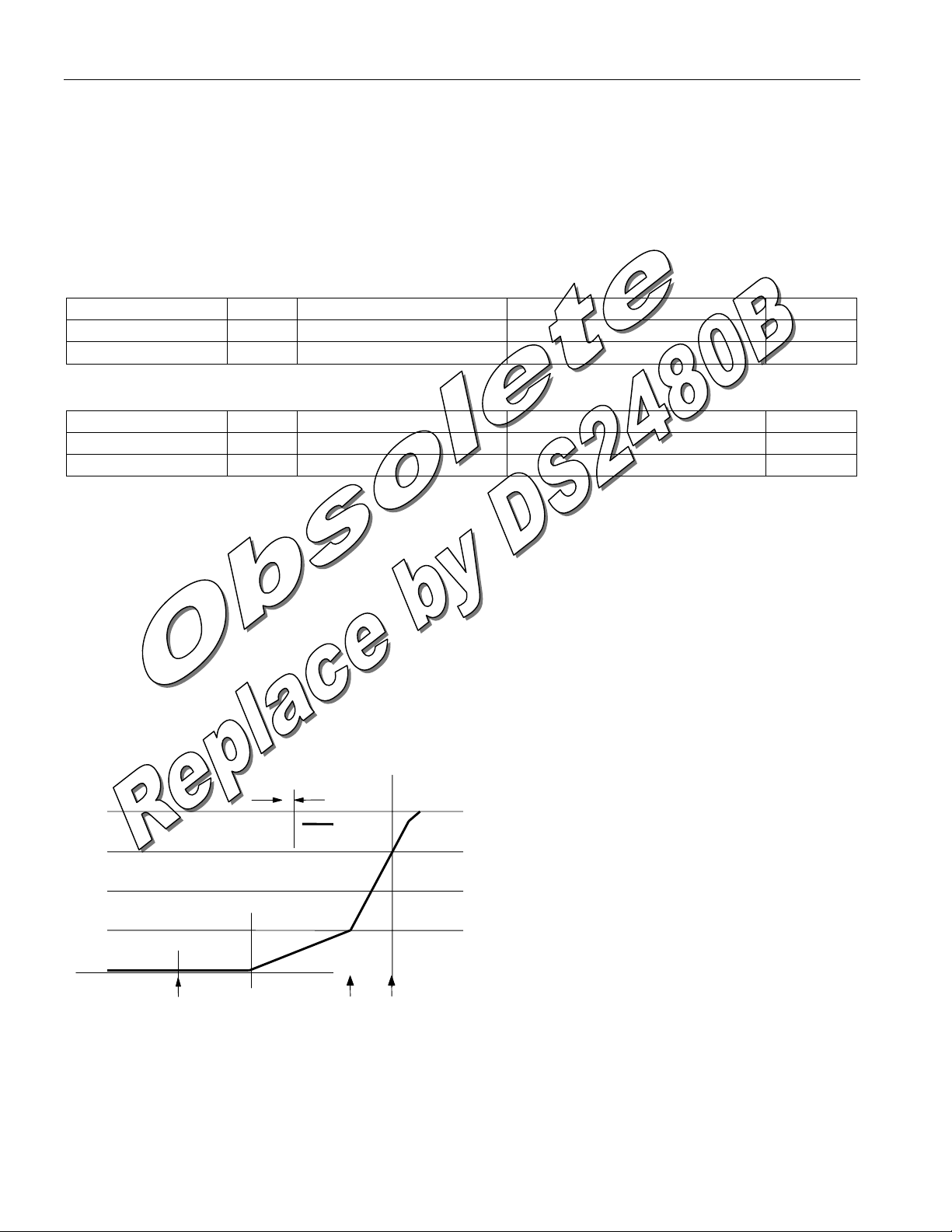
1-WIRE COMMUNICATION WAVE FORMS
One of the major features of the DS2480 is that it relieves the host from generating the timing of the
1-Wire signals and sampling the 1-Wire bus at the appropriate times. How this is done for the
reset/presence detect sequence is shown in Figure 6a. This sequence is composed of four timing
segments: the reset low time t
offset t
and a delay time t
PDT
FILL
, the short/interrupt sampling offset tSI, the presence d etect sampling
RSTL
. The timing segments tSI, t
PDT
and t
comprise the reset high time t
FILL
RSTH
where 1-Wire slave devices assert their presence or interrupt pulse. Durin g this time the DS2480 pulls the
1-Wire bus high with its weak pull-up current.
The values of all timing segments for all 1-Wire speed options are shown in the table. Since the
reset/presence sequence is slow compared to the time slots, the values for regular and flexible speed are
the same. Except for the falling edge of the presence pulse all edges are controlled b y the DS2480. The
shape of the uncontrolled falling edge is determined by the capacitance of the 1-Wire bus and the number,
speed and sink capability of the slave devices connected.
RESET/PRESENCE DETECT Figure 6a
5V
UNCONTROLLED
0V
TESTING FOR SHORT AND/OR INTERRUPT
Speed t
t
RSTL
FALLING EDGE
RSTL
RESET/PRESENCE SEQUENCE
t
t
SI
t
SI
PDT
t
RSTH
PRESENCE
PULSE
t
FILL
PRESENCE TESTING
t
PDT
IDLE
TIME
TIME
SLOT
t
FILL
t
RSTH
Regular 512 µs 8 µs 64 µs 512 µs 584 µs
Overdrive 64 µs 2 µs 8 µs 64 µs 74 µs
Flexible 512 µs 8 µs 64 µs 512 µs 584 µs
After having received the command code for generating a reset/presence sequence, the DS2480 pulls the
1-Wire bus low for t
and then lets it go back to 5-volts. The DS2480 will now wait for the
RSTL
short/interrupt sampling offset tSI to expire and then test the voltage on the 1-Wire bus to determine if
there is a short or an interrupt signal. If there is no short or interrupt (as shown in the picture), the DS2480
will wait for t
the presence test, the DS2480 will then wait for t
and test the voltage on the 1-Wire bus for a presence pulse. Regardless of the result of
PDT
to expire and then send the command response byte
FILL
to the host.
If the test for interrupt or short reveals a logic 0, the DS2480 will wait for 4096 ∝s and then test the
1-Wire bus again. If a logic 0 is detected, the 1-Wire bus is shorted and a command response byte with
the code for SHORT will be sent immediately. If a logic 1 is detected, the device will wait for t
FILL
to
expire after which it will send the command response byte with the code for an alarming presenc e pulse.
No additional testing for a presence pulse will be done. The DS2480 will perform the short/interrupt
testing as described also at Overdrive speed, although interrupt signaling is only defined for regular
speed.
The idle time following the Reset/Presence Detect sequence depends on the serial communication speed
and the host’s response time.
A Write 1 and Read Data time slot is comprised of the segments t
time slots, after the write 1 low time t
is over, the DS2480 waits for the duration of the data s ample
LOW1
LOW1
DSO
and t
. During write 1
HIGH
, t
offset and then samples the voltage at the 1-Wire bus to read the response. After this, the waiting time
t
must expire before the time slot is complete. A Write 0 time slot only consists of the two segments
HIGH1
t
LOW0
and t
REC0
.
15 of 28
Page 16

DS2480
If the network is large or heavily loaded, one should select flex ible speed and extend t
to more than
LOW1
8 µs to allow the 1-Wire bus to completely discharge. Since a large or heavily loaded network needs more
time to recharge, it is also recommended to delay sampling the bus for reading. A higher value for t
DSO
will increase the voltage margin and also provide extra energy to the slave devices when generating a
long series of write 0 time slots. However, the total of t
LOW1
+ t
should not exceed 22 µs*. Otherwise
DSO
the slave device responding may have stopped pulling the bus low when transmitting a logic 0.
The idle time between time slots within a byte or during a 12-bit sequence while the Search Accelerator is
on is zero. Between bytes, 12-bit search sequences and single bits the idle time depends on the RS232
data rate and the host’s response time. The response byte is sent to the host as soon as the l ast time slot of
a byte, 12-bit sequence or the command is completed.
WRITE 1 AND READ DATA TIME SLOT Figure 6b
5V
0V
t
LOW1
Speed t
TIME SLOT DURATION t
t
SAMPLING
LOW1
SLOT
t
DSO
Regular 8 µs 3 µs 49 µs 60 µs
Overdrive 1 µs 1 µs 8 µs 10 µs
Flexible 8 to 15 µs 3 to 10 µs 49 µs 60 to 74 µs
IDLE
TIME
NEXT
T.S.
t
HIGH1
t
SLOT
*
WRITE 0 TIME SLOT Figure 6c
REC0
IDLE
TIME
NEXT
T.S.
t
SLOT
*
5V
0V
t
RECO
Speed t
t
LOW0
*t
LOW0
Regular 57 µs 3 µs 60 µs
Overdrive 7 µs 3 µs 10 µs
Flexible 57 µs 3 to 10 µs 60 to 67 µs
*In a 5-volts environment (± 1-volt, full temperature range) the tolerance of the internal time base of
1-Wire slave devices is much narrower than what it is when operated at the minimum voltage of 2.8 volts.
Therefore, the timing generated by the DS2480 is in compliance with the requirements of all MicroLANcompatible 1-Wire devices.
16 of 28
Page 17

DS2480
PULSE WAVE FORMS, DISARMED
The pulse command can be used to generate a strong pull-up to 5-volts and a 12-volts programming
pulse, respectively. The duration of the pulse is predefined if the parameter value code of par ameter 010
(Programming Pulse Duration) and parameter 011 (Strong Pull-Up Duration), has a value from 000 to
110 (see Table 4). Figures 7a and 7b show the timing of a pulse with predefined duration, which should
be considered the normal case. If an infinite duration is chosen (parameter value code 111), the host must
terminate the pulse command, as shown in Figures 7c and 7d. All versions of Figure 7 assume that bit 1
of the pulse command is 0, i.e., disarmed mode. See section Communication Commands, Pulse, for more
details on possibilities of the pulse command.
STRONG PULL-UP TO 5V, PREDEFINED DURATION Figure 7a
IDLE
END OF PREVIOUS
5V
0V
TIME SLOT
TIME
t
t
1
2
t
SPU
t
The processing of a pulse command is essentially the same, regardless if a strong pull-up or a
programming pulse is requested. At t1 the host starts sending the pulse command byte. At t2 the DS2480
has received the command and immediately generates the pulse. The pulse ends at t3 and the DS2480
sends out the command response byte to inform the host that the command is completed. The idle time
between t1 and t2 is determined by the time to transmit the command byte at the selected baud rate. The
idle time between t3 and t4 is comprised of the time to transmit the response byte, plus the response time
of the host plus the time to transmit the command and/or data to generate the next time slot.
IDLE
TIME
3
BEGIN OF NEXT
TIME SLOT
t
4
12V PROGRAMMING PULSE, PREDEFINED DURATION Figure 7b
12V
END OF PREVIOUS
5V
0V
TIME SLOT
IDLE
TIME
t
2
A correct programming pulse can only be generated if the 12-volts programming voltage is available at
the Vpp pin of the DS2480. The slew rate of the rising and falling edge of the programming pulse (“steep
slopes”) is not actively controlled by DS2480. For EPROM programming, only a single slave device
should be connected to the 1-Wire bus and the cable must to be short, not to exceed a few meters. One
should not attempt generating a programming pulse with a non-EPROM device on the bus; this may
damage the device as well as the DS2480. Certain applications may require a duration for a stron g pullup or programming pulse that cannot be realized using one of the predefined values. Selecting infinite
duration allows the host to generate pulses of any length. As a consequence, however, the host becomes
responsible to actively control the duration of the pulse. Failing to do so may require a power-on reset or
master reset cycle of the DS2480. For this reason, infinite duration should only be used if absolutely
necessary. The time to end a pulse of infinite duration strongly depends on the baud rate of the
STEEP SLOPES
t
PP
IDLE
TIME
t
3
BEGIN OF NEXT
TIME SLOT
t
4
17 of 28
Page 18

DS2480
communication between host and DS2480. Neglecting the response time of the host, the minimum pulse
durations are: 86.8 µs at 115.2 kbps, 173.6 µs at 57.6 kbps, 520 µs at 19.2 kbps and 1.04 ms at 9.6 kbps.
STRONG PULL-UP TO 5V, INFINITE DURATION Figure 7c
END OF PREVIOUS
5V
0V
TIME SLOT
IDLE
TIME
t
1
t
2
STRONG PULL-UP ON
t
3
As before, processing the command is essentially the same, regardless if it is for a strong pull-up or a
programming pulse. At t1 the host starts sending the pulse command byte. At t2 the DS2480 has received
the command and immediately activates the strong pull-up or switches in the 12V programming voltage.
To end the pulse, the DS2480 must receive a termination command, code F1h, which occurs at t3. The
termination command does not generate a response byte. The DS2480 will immediately end the pulse and
send out the response byte of the pulse command. The idle time between t1 and t2 is determined by the
time to transmit the command byte at the selected baud rate. The idle time between t3 and t4 is comprised
of the time to transmit the pulse response byte, plus the response time of the host plus the time to transmit
the command and/or data to generate the next time slot.
IDLE
TIME
BEGIN OF NEXT
TIME SLOT
t
4
12V PROGRAMMING PULSE, INFINITE DURATION Figure 7d
12V
END OF PREVIOUS
5V
0V
TIME SLOT
IDLE
TIME
t
2
STEEP SLOPES
PROGRAMMING VOLTAGE
IS APPLIED
IDLE
TIME
t
3
BEGIN OF NEXT
TIME SLOT
t
4
PULSE WAVE FORM, ARMED
As explained in section Communication Commands, bit 1 of the pulse command allows the arming of a
strong pull-up to 5-volts if the bit is set to 1. If the strong pull-up is armed and the device is switched to
data mode, there will be a strong pull-up immediately following every byte on the 1-Wire bus. This mode
is implemented to provide extra energy when writing to EEPROM devices or to do a temperature
conversion with the DS1920 Temperature iButton, for example. These devices need a strong pull-up
immediately after the power-consuming activity has been initiated by a command code.
To arm the strong pull-up, one usually generates a “dummy” pulse with bit 1 being 1 while the device is
in command mode. To save time, the dummy pulse may immediately be terminated by sending the
termination command, code F1h. Then one switches to data mode and sends a command code that makes
one or more slaves on the 1-Wire bus require extra energy. After the command execution is finished, one
switches back to command mode and disarms the strong pull-up by generating another dumm y pulse. A
complete temperature conversion sequ ence that shows the use of the armed pulse is included i n Section
“Software DriverExamples”.
18 of 28
Page 19

DS2480
STRONG PULL-UP TO 5-VOLTS, ARMED, PREDEFINED DURATION Figure 8
END OF 8th
TIME SLOT
5V
0V
t
SPU
IDLE
TIME
BEGIN OF NEXT
TIME SLOT
t
1
t
2
t
3
Figures 8 shows the timing of the strong pull-up in data mode. At t1 the 8th time slot of the byte sent to
the 1-Wire bus is completed. Without any delay the DS2480 now activates the strong pull-up and
simultaneously starts sending the data response byte to the host. At t
DS2480 sends a pulse response byte to the host. The idle time between t
the strong pull-up ends and the
2
and t3 is comprised of the time
2
to transmit the pulse response byte, plus the response time of the host plus the time to transmit the
command and/or data to generate the next time slot.
Since in data mode the pulse termination command is not applicable, the duration of the strong pull-up
must be limited. See Table 4, parameter 011 (Strong Pull-Up Duration) for details. Selecting infinite
duration will require a power-on or master reset cycle to get the DS2480 back to communicating with the
host.
SINGLE BIT WITH STRONG PULL-UP
Similar to the pulse command the Single Bit command also allows generating a strong pull-up
immediately following a time slot. The strong pull-up of the Single Bit command, however, is controlled
directly by bit 1 of the command code and therefore needs not be armed. Since the DS2480 remains in
command mode when using the Single Bit command, any duration of the strong pull-up including infinite
may be selected. Figure 9 shows the timing of the Single Bit command with the immediately following
strong pull-up. Strong pull-up immediately following a single time slot is implemented to support the
DS1954 CryptoiButton. After having received the command code to run a pro gram, the CryptoiButton
sends out an acknowledge bit and then starts the microcomputer to run the firmware program for a
predefined time.
SINGLE BIT WITH STRONG PULL-UP, PREDEFINED DURATION Figure 9a
IDLE
TIME
2
BEGIN OF NEXT
ACTIVITY
t
3
5V
0V
END OF PREVIOUS
TIME SLOT
t
1
t
SPU
t
For predefined duration (Figure 9a) the timing is as follows: At t1 the time slot is completed. Now the
DS2480 activates the strong pull-up and simultaneously starts sending the response byte of the Single Bit
command to the host. At t2 the strong pull-up ends and the DS2480 sends out a pulse response byte. The
idle time between t2 and t3 is comprised of the time to transmit the pulse response byte, plus the response
time of the host plus the time to transmit the command and/or data to generate the next time slot. For
infinite duration (Figure 9b) the strong pull-up also begins immediately after the time slot is completed.
To end the strong pull-up, the DS2480 must receive a termination command, code F1h, which occurs at
. The termination command does not generate a response byte. The DS2480 will then immediately end
t
2
19 of 28
Page 20

DS2480
the strong pull-up and send out a pulse response byte. Everything else is the same as with predefined
duration.
SINGLE BIT WITH STRONG PULL-UP, INFINITE DURATION Figure 9b
END OF PREVIOUS
5V
0V
STRONG PULL-UP ON
IDLE
TIME
BEGIN OF NEXT
ACTIVITY
t
1
t
2
t
3
The minimum duration of a strong pull-up of infinite duration strongly depends on the baud rate of the
communication between host and DS2480. The host must first receive the response byte of the single-bit
command, react to it and then transmit the termination command. Neglecting the hosts response time, the
shortest duration of an infinite strong pull-up therefore is173.6 µs at 115.2 kbps, 347.2 µs at 57.6 kbps,
1.04 ms at 19.2 kbps and 2.08 ms at 9.6 kbps.
SOFTWARE DRIVER EXAMPLES
The DS2480 requires a software driver that translates the activities to be generated on the 1-Wire bus into
the appropriate commands. The examples below cover typical situations, such as reading the ROM,
writing to the scratchpad of a Memory iButton, reading the memory of a Memory iButton, programming
an Add-Only iButton EPROM and performing a temperature conversion with the Temperature iButton
DS1920. An example for the use of the Search Accelerator is included in the description of the Search
Accelerator, earlier in this document. The DS2480 command codes used in these examples are valid for
regular speed and will work properly on short 1-Wire busses (< 10 meters). The response b yte on the
reset command assumes a normal presence pulse, no alarm or short. The DS2480 includes a 1-byte
buffer that stores a byte received from the host while the previous byte is being translated into activity on
the 1-Wire bus. For this reason the host may send another byte even without having received the response
byte. Sending bytes faster than they can be translated into 1-Wire activities may result in loss of data
and/or synchronization and therefore should be avoided.
READ ROM SEQUENCE
Action Sequence Host TX Host RX
Generate Reset Pulse C1 C9
Set data mode E1 (nothing)
Read ROM Command 33 (as sent)
Read ROM ID (8 bytes) FF (x8) ROM ID
Set command mode E3 (nothing)
Generate Reset Pulse C1 C9
20 of 28
Page 21

WRITE SCRATCHPAD SEQUENCE
Write 2 bytes to scratchpad at memory locations 16h and 17h
Action Sequence Host TX Host RX
Generate Reset Pulse C1 C9
Set data mode E1 (nothing)
Skip ROM Command CC CC
Write Scratchpad Cmd. 0F (as sent)
Starting Address TA1 16 (as sent)
Starting Address TA2 00 (as sent)
Write to the Scratchpad (2 bytes) (as sent)
Set command mode E3 (nothing)
Generate Reset Pulse C1 C9
READ MEMORY SEQUENCE
Read 8 bytes from memory address 0040h
Action Sequence Host TX Host RX
Generate Reset Pulse C1 C9
Set data mode E1 (nothing)
Skip ROM Command CC (as sent)
Read Memory Command F0 (as sent)
Starting Address TA1 40 (as sent)
Starting Address TA2 00 (as sent)
Read 8 bytes of data FF (x8) data
Set command mode E3 (nothing)
Generate Reset Pulse C1 C9
DS2480
WRITE EPROM SEQUENCE (DS2505)
Write memory starting at address 40h
Action Sequence Host TX Host RX
Set Vpp dur. = 512====∝∝∝∝s
Generate Reset Pulse C1 C9
Set data mode E1 (nothing)
Skip ROM Command CC (as sent)
Write Memory Command 0F (as sent)
Starting Address TA1 40 (as sent)
Starting Address TA2 00 (as sent)
*** Send data byte (data) (as sent)
Receive CRC16 FF (x2) CRC16
Set command mode E3 (nothing)
Generate Program Pulse FD response
Set data mode E1 (nothing)
Read written byte FF (data)
Go to *** to write the next byte or end the sequence as shown below.
Set command mode E3 (nothing)
Generate Reset Pulse C1 C9
29 28
21 of 28
Page 22

DS2480
TEMPERATURE CONVERSION SEQUENCE
Action Sequence Host TX Host RX
Set pull-up dur. = 524 ms 39 38
Generate Reset Pulse C1 C9
Set data mode E1 (nothing)
Skip ROM Command CC (as sent)
Set command mode E3 (nothing)
Arm strong pull-up EF (nothing)
Terminate pulse F1 response
Set data mode E1 (nothing)
Convert Temperature 44 (as sent)
Wait for pulse response (nothing) response
Set command mode E3 (nothing)
Disarm strong pull-up ED (nothing)
Terminate pulse F1 response
Generate Reset Pulse C1 C9
HARDWARE APPLICATION EXAMPLES
This section discusses five typical application scenarios of the DS2480. When directly designed into a
new product, the device can be connected as shown in Figure 10a. The ci rcuit becomes more complex if
a 1-Wire bus is to be interfaced to a port that provides and expects inverted signals, but does not
necessarily meet the RS232C (± 12-volts) standard (Figure 10b).
UART DIRECT Figure 10a
UART
OR ∝C
SIN (RXD)
SOUT (TXD)
LM
+/(-) 5V RS232 Figure 10b
POWER
STEALING
DTR
RTS
RXD
TXD
GND
LM
UART
OR ∝C
DRIVER/
LEVEL SHIFTER
1
0
1
STOP0
VOLTAGE
REGULATOR
STOP
5V
12V
(5V)
5V
SEE TEXT
12V
(5V)
V
PP
RXD
TXD
V
DD
DS2480
GND
V
PP
RXD
DS2480
TXD
GND
V
DD
POL
1-WIRE BUS
1-W
RETURN
POL
1-W
1-WIRE BUS
RETURN
22 of 28
Page 23

DS2480
The signals DTR and RTS provide the power to operate the DS2480. The resistor in the TXD line and the
Schottky diode limit the negative voltage at the TXD pin of the DS2480 to 0.3 volts maximum. The
resistor is typically 4.7 kΩ. If the inverting driver is current-limited to 1 mA the resistor is not required.
From the DS2480’s perspective, this circuit will work with inverted signals of ± 5-volts as well as 0 to
5-volts. Depending on the voltage levels the host expects, it may be necessary to generate a negative
voltage on the RXD line. Figure 10c shows how this can be accomplished for a true RS232C system.
+ 12V RS232 Figure 10c
5V
POWER
STEALING
DTR
RTS
UART
OR ∝C
RXD
2.7 k
TXD
1∝
GND
In the interface to a true RS232C system (± 12-volts, Figure 10c) the power for the DS2480 is stolen from
DTR and RTS. The software must make sure that at least one of these signals constantly provides the
12-volts operating voltage. The 6.8 kΩ resistor and the 4.7 volts Zener diode in the TXD line limit the
positive voltage at the TXD pin of the DS2480. The Schottky diode limits the negative voltage to
0.3 volts maximum. The Schottky diode in series with the capacitor forms a parasitic supply to gener ate
the negative bias for the host’s receive channel. The positive signal is switched in through the P-channel
MOSFET that connects to the RXD output of the DS2480. In this circuit diagram the MOSFET switches
the RXD line to +5-volts, which normally is sufficient for RS232Csystems. Switching to 12-volts is also
possible, but requires a P-channel transistor with a different threshold voltage. The signal inversion
caused by the transistor is compensated through the DS2480 by using a value code of 100, 101, 110 or
111 for the RS232 baud rate setting.
VOLTAGE
REGULATOR
6.8 k
4.7V
S
D
SEE TEXT
STOP
BSS110
0
LM
1
12V
(5V)
V
PP
RXD
TXD
V
DD
DS2480
GND
POL
1-WIRE BUS
1-W
RETURN
23 of 28
Page 24

DS2480
UART DIRECT OPTO ISOLATED Figure 10d
The circuit in Figure 10d is essentially the same as in Figure 10a. The main difference is the optoisolation. The characteristics of the opto-isolators are not very critical. Using a different t ype will affect
the values of the resistors that limit the current through the LEDs and bias the photo transistors.
+ 5 TO 12V RS232 OPTO ISOLATED Figure 10e
The circuit in Figure 10e combines the true RS232C interface with opto-isolation. The energy to power
the LED in the TXD channel and to provide the positive voltage for the host’s RXD input is stolen from
DTR and RTS. The negative voltage for the RXD input is taken from the TXD line through a parasitic
supply consisting of a Schottky diode in series with a capacitor. The HCPL-2202 opto-isolator has a
totem pole output that allows switching in positive as well as negative voltage. The +5-volts are sufficient
for most RS232C systems. Switching in 12-volts requires a opto-isolator with different voltage
characteristics. In the schematic the HCPL-2202 opto-isolator is sourced by the RXD pin of the DS2480.
It can as well be connected the traditional way where the DS2480 sinks the current through the LED.
This, however, causes a signal inversion that has to be compensated through the DS2480 by using a value
code of 100, 101, 110 or 111 for the RS232 baud rate setting. Using other t ypes of opto-isolators than
shown in the schematic will at least require changing the values of the resistors.
24 of 28
Page 25

DS2480
RS232 DATA TIMING RXD LINE Figure 11
t
FR
START
BIT 0
t
RR
BIT 1 BIT 2 BIT 3 BIT 4 BIT 5 BIT 6 BIT 7 STOP
T
R
(DIAGRAM DRAWN FOR POL = 5V)
10 T
R
RECEIVE DELAY TIMING Figure 12
BIT 6 BIT 7 STOP
TXD
INPUT SAMPLING 8.5TR9.5T
R
(DIAGRAM DRAWN FOR POL = 5V)
START
RXD
RS232 DATA TIMING TXD LINE Figure 13
BIT 0 BIT 1 BIT 2 BIT 3 BIT 4 BIT 5 BIT 6 BIT 7 STOP
T
T
V
V
IL
IH
1.5 T
R
2.5 TR3.5 TR4.5 TR5.5 TR6.5 TR7.5 TR8.5 TR9.5 T
TT = 1/BAUD RATE OF UART
DIAGRAM DRAWN FOR POL = 5V)
10 T
T
TR = 1/BAUD RATE OF DEVICE
BIT
t
t
IDLER
IDLET
R
25 of 28
Page 26

FUNCTION AND SPEED MATRIX Table 7
1-Wire Speed
Baud Rate Regular Flexible Overdrive Function
9600 bps
√√ √
√√ √
19200 bps X X
√
X
57600 bps X X
XX
√
√
√
√
115200 bps X X X Search
XX
√
Search
Command/Data
Search
Command/Data
Search
Command/Data
Command/Data
DS2480
√ t
X not recommended unless t
is guaranteed by the UART; no precautions necessary
IDLET
IDLET
TXD LINE ASYMMETRY Figure 14
is controlled by the host through a wait function
26 of 28
Page 27

DS2480
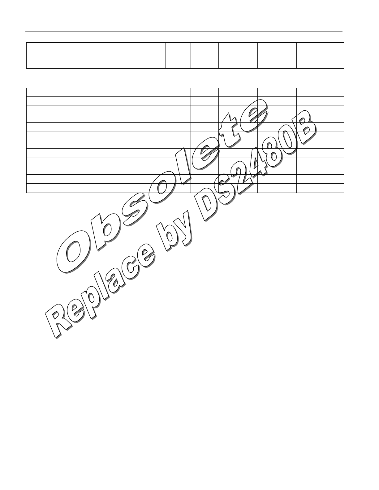
ABSOLUTE MAXIMUM RATINGS*
Voltage on 1-W to Ground -0.5V to +14.0V
Voltage on RXD, TXD, POL to Ground -0.5V to +7.0V
Operating Temperature -40°C to +85°C
Storage Temperature -55°C to +125°C
Soldering Temperature See J-STD-020A Specification
* This is a stress rating only and functional operation of the device at these or any other conditions above
those indicated in the operation sections of this specification is not implied. Exposure to absolute
maximum rating conditions for extended periods of time may affect reliability.
DC ELECTRICAL CHARACTERISTICS (VDD = 4.5V to 5.5V;-40°C to 85°C)
PARAMETER SYMBOL MIN TYP MAX UNITS NOTES
Supply Voltage V
Programming Voltage V
Operating Current I
Idle Current on V
PP
I
Active Pull-up Timer Threshold V
Active Pull-up On Threshold V
1-Wire Input High V
1-Wire Input Low V
TXD/POL input resistor R
TXD/POL input levels V
TXD/POL input levels V
1-Wire weak pull-up current I
1-Wire active pull-up current I
Strong pull-up voltage drop
∆V
@ 10 mA load on 1-W
Programming voltage drop
∆V
@ 10 mA load on 1-W
RXD sink current @ 0.4V I
RXD source current @ VDD-0.4V I
Power On Reset Trip Point V
VPP Sensor Trip Point V
CC
PP
DD
PP
IAPTO
IAPO
IH1
IL1
I
IH
IL
WEAKPU
ACTPU
STRPU
PROG
OLR
OHR
POR
PPTRIP
4.5 5.0 5.5 V
11.75 12.25 V 1
3.0 5.0 mA
20 µA 2
VDD-1.4 VDD-1.1 V
0.95 1.2 V
3.4 V
1.8 V
30
kΩ
3
2.7 V
0.8 V
1.5 3.0 5.0 mA
915 mA
0.6 V 4
0.24 V 5
6mA
-4 mA
3.3 V
9.5 V
27 of 28
Page 28
DS2480
CAPACITANCES (tA = 25°C)
PARAMETER SYMBOL MIN TYP MAX UNITS NOTES
TXD/POL input capacitance C
1-Wire input capacitance C
IN
IN1
5pF
10 pF
AC ELECTRICAL CHARACTERISTICS (VDD = 4.5V to 5.5V;-40°C to 85°C)
PARAMETER SYMBOL MIN TYP MAX UNITS NOTES
UART Bit Time T
Device Bit Time T
Fall Time RXD t
Rise Time RXD t
Transmit Idle Time t
Receive Idle Time t
Asymmetry t
Arrival Response Time t
Master Reset Time t
Active Pull-Up on Time t
Response Time t
T
R
FR
RR
IDLET
IDLER
ASYM
ARR
MR
APUOT
RESP
8.68 104 µs 6
8.68 104 µs 6, 7
820ns8
13 27 ns 8
0µs9
t
IDLET
µs
1µs10
4.4 52 µs 11
104 µs 12
0.5 2.0 µs 13
8.68 + ∆ 104 + ∆
µs 11, 14
NOTES:
1. VPP - ∆V
2. Applies only if a 12.0V supply is connected. If VPP and VDD are tied together, current is less than
1 µA.
3. Input load is to GND.
4. Voltage difference between VDD and 1-W.
5. Voltage difference between VPP and 1-W.
6. 8.68 µs (115.2 kbps), 52 µs (19.2 kbps), 17.36 µs (57.6 kbps), 104 µs (9.6 kbps).
7. Nominal values; tolerance = ±5%.
8. At VCC = 5.0V and 100 pF load to GND.
9. See Table 7, Function and Speed Matrix.
10. Independent of baud rate.
11. Minimum at 115.2 kbps, maximum at 9.6 kbps.
12. The master reset cycle is complete after t
13. Minimum value at Overdrive speed; maximum value at regular speed.
14. ∆=is the time to complete the activity on the 1-Wire bus; values range from 0 (configuration
command) up to5130 µs (alarming presence pulse)
must be within 11.5 to 12.0V.
PROG
is over.
MR
28 of 28
 Loading...