

Page 1
www.maxim-ic.com.cn
概述
®
DS2431 是一款 1024 位 1-Wire
EEPROM 芯片,由
四个存储器页组成,每页 256 位。数据先被写入一个
8 字节暂存器中,经校验无误后复制到 EEPROM 存储
器。其特点在于,四个存储器页相互独立,可以单独
设置写保护或 EPROM 仿真模式,在 EPROM 仿真模
式下,所有位的状态只能从 1 变成 0。DS2431 通过一
根 1-Wire 总线进行通信。通信采用 Dallas
Semiconductor 标准的 1-Wire 协议。每个器件都有唯
一 的、不能更改的 64 位 ROM 地址码,该地址码由工
厂光刻写入芯片。在一个多点的 1-Wire 网络环境中,
该地址码用于对器件进行寻址。
应用
附件/PC 板识别
医疗传感器校准数据存储
模拟传感器校准,包括 IEEE-P1451.4 智能传感器
墨盒/碳粉打印盒识别
消费类产品的售后管理
典型工作电路
V
CC
R
PUP
DS2431
1024 位 1-Wire EEPROM
特性
1024 位 EEPROM 存储器,分为四页,每页 256
位。
独立的存储器页,可以永久写保护或设置成
EPROM 仿真模式(“写入 0”)。
通过切换点滞回与滤波,对噪声条件下的性能进
行优化。
IEC 1000-4-2 Level 4 ESD 保护(8kV 接触模式,
15kV 气隙放电模式)。
可在-40°C 至+85°C 温度范围,2.8V 至 5.25V 的
宽电压范围内进行读写操作。
按照 1-Wire 协议,在 15.4kbps 或 111kbps 速率
下使用单独数字信号与主机通信。
定购信息
PART TEMP RANGE PIN-PACKAGE
DS2431 -40°C to 85°C TO-92
DS2431/T&R -40°C to 85°C TO-92, tape & reel
DS2431P -40°C to 85°C TSOC
DS2431P/T&R -40°C to 85°C TSOC, tape & reel
DS2431X -40°C to 85°C CSP, tape & reel
引脚配置
µC
I/O
DS2431
GND
为了区分清楚,命令,寄存器,模式均为大写
1-Wire是 Dallas Semiconductor Corp.
本文是Maxim正式英文资料的译文,Maxim不对翻译中存在的差异或由此产生的错误负责。请注意译文中可能存在文字组织或翻译错误,如需确认任何词语
的准确性,请参考Maxim提供的英文版资料。
索取免费样品和最新版的数据资料,请访问Maxim的主页:www.maxim-ic.com.cn
1 of 24
的一个注册商标。
。
081604
Page 2
DS2431: 1024 位 1-Wire EEPROM
ABSOLUTE MAXIMUM RATINGS
I/O Voltage to GND -0.5V, +6V
I/O Sink Current 20mA
Operating Temperature Range -40°C to +85°C
Junction Temperature +150°C
Storage Temperature Range -40°C to +85°C
Soldering Temperature See IPC/JEDEC J-STD-020A
Stresses beyond those listed under “Absolute Maximum Ratings” may cause permanent damage to the device. These are stress ratings only,
and functional operation of the device at these or any other conditions beyond those indicated in the operational sections of the specifications is
not implied. Exposure to the absolute maximum rating conditions for extended periods may affect device reliability.
ELECTRICAL CHARACTERISTICS
(V
= 2.8V to 5.25V, T
PUP
PARAMETER SYMBOL CONDITIONS MIN TYP MAX UNITS
I/O PIN GENERAL DATA
1-Wire Pullup Resistance
Input Capacitance CIO (Notes 3, 4) 100 800 pF
Input Load Current I
High-to-Low Switching
Threshold
Input Low Voltage V
Low-to-High Switching
Threshold
Switching Hysteresis V
Output Low Voltage V
Recovery Time
(Notes 1,11)
Rising-Edge Hold-off Time t
Timeslot Duration (Note 1) t
I/O PIN, 1-WIRE RESET, PRESENCE DETECT CYCLE
Reset Low Time (Note 1) t
Presence Detect High
Time
Presence Detect Fall Time
(Notes 4, 14)
Presence Detect Low
Time
Presence Detect Sample
Time (Note 1)
= -40°C to +85°C.)
A
R
PUP
L
V
TL
IL
V
TH
HY
OL
t
REC
REH
SLOT
RSTL
t
PDH
t
FPD
t
PDL
t
MSP
(Notes 1, 2)
I/O pin at V
0.05 2.2 µA
PUP
0.3 2.2
kΩ
(Notes 4, 5, 6) 0.46 4.4 V
(Notes 1, 7) 0.3 V
(Notes 4, 5, 8) 1.0 4.9 V
(Notes 4, 5, 9) 0.21 1.70 V
At 4mA (Note 10) 0.4 V
Standard speed, R
Overdrive speed, R
PUP
PUP
= 2.2kΩ
= 2.2kΩ
Overdrive speed, directly prior to reset
pulse; R
PUP
= 2.2kΩ
Standard speed (Note 12) 0.5 5.0
Overdrive speed Not applicable (0)
Standard speed 65
Overdrive speed (Note 13) 9
5
2
5
µs
µs
µs
Standard speed, V
Standard speed (Note 12) 504 640
Overdrive speed, V
Overdrive speed (Note 13)
Standard speed, V
Standard speed (Note 13) 15 63
Overdrive speed (Note 13) 2
Standard speed, V
Standard speed 1.1 7
> 4.5V 480 640
PUP
> 4.5V 48 80
PUP
53 80
> 4.5V 15 60
PUP
> 4.5V 1.1 3.75
PUP
µs
µs
7
µs
Overdrive speed 1.1
Standard speed 60 240
Overdrive speed, V
Overdrive speed (Note 13) 8
Standard speed, V
> 4.5V 8 24
PUP
> 4.5V 64 75
PUP
26
Standard speed 70 75
µs
µs
Overdrive speed 8.1 10
2 of 24
Page 3
DS2431: 1024 位 1-Wire EEPROM
PARAMETER SYMBOL CONDITIONS MIN TYP MAX UNITS
I/O PIN, 1-Wire WRITE
Write-0 Low Time (Note 1) t
Write-1 Low Time
(Notes 1, 15)
I/O PIN, 1-Wire READ
Read Low Time
(Notes 1, 16)
Read Sample Time
(Notes 1, 16)
EEPROM
Programming Current I
Programming Time t
(Endurance)
W0L
t
W1L
t
RL
t
MSR
PROG
PROG
N
CY
Standard speed 60 120
Overdrive speed (Note 13) 7 16
Standard speed 5
Overdrive speed 1
Standard speed 5
Overdrive speed 1
Standard speed
Overdrive speed
(Note 17) 1 mA
(Note 18) 12.5 ms
At 25°C 200k Write/Erase Cycles
At 85°C (worst case) 50k
µs
15 - ε
2 - ε
µs
15 - δ
2 - δ
t
+ δ
RL
t
+ δ
RL
15
2
µs
µs
---
Data Retention tDR At 85°C (worst case) 10 years
Note 1: System requirement.
Note 2: Maximum allowable pullup resistance is a function of the number of 1-Wire devices in the system and 1-Wire recovery times. The
Note 3:
Note 4: Guaranteed by design, simulation only. Not production tested.
Note 5: V
Note 6: Voltage below which, during a falling edge on I/O, a logic 0 is detected.
Note 7: The voltage on I/O needs to be less or equal to V
Note 8: Voltage above which, during a rising edge on I/O, a logic 1 is detected.
Note 9: After V
Note 10: The I-V characteristic is linear for voltages less than 1V.
Note 11: Applies to a single DS2431 attached to a 1-Wire line.
Note 12: The earliest recognition of a negative edge is possible at t
Note 13: Highlighted numbers are NOT in compliance with legacy 1-Wire product standards. See comparison table below.
Note 14: Interval during the negative edge on I/O at the beginning of a Presence Detect pulse between the time at which the voltage is
Note 15:
Note 16:
Note 17: Current drawn from I/O during the EEPROM programming interval. The pullup circuit on I/O during the programming interval
Note 18: Interval begins t
LEGACY VALUES DS2431 VALUES
MIN MAX MIN MAX MIN MAX MIN MAX
t
SLOT
t
RSTL
t
PDH
t
PDL
t
W0L
1)
Intentional change, longer recovery time requirement due to modified 1-Wire front end.
specified value here applies to systems with only one device and with the minimum 1-Wire recovery times. For more heavily
loaded systems, an active pullup such as that found in the DS2482-x00, DS2480B, or DS2490 may be required.
Capacitance on the data pin could be 800pF when V
after V
80% of V
ε represents the time required for the pullup circuitry to pull the voltage on I/O up from V
δ represents the time required for the pullup circuitry to pull the voltage on I/O up from V
master.
should be such that the voltage at I/O is greater than or equal to Vpup(min). If Vpup in the system is close to Vpup(min) then a
low impedance bypass of Rpup which can be activated during programming may need to be added.
sequence. Interval ends once the device's self-timed EEPROM programming cycle is complete and the current drawn by the
device has returned from I
has been applied the parasite capacitance will not affect normal communications.
PUP
, VTH, and V
TL
TH
are a function of the internal supply voltage.
HY
is crossed during a rising edge on I/O, the voltage on I/O has to drop by at least VHY to be detected as logic '0'.
and the time at which the voltage is 20% of V
PUP
after the leading negative edge on IO for the last timeslot of the E/S byte for a valid Copy Scratchpad
WiLMIN
to IL.
PROG
is first applied. If a 2.2kΩ resistor is used to pull up the data line, 2.5µs
PUP
whenever the master drives the line low.
ILMAX
after VTH has been previously reached.
REH
.
PUP
to VTH.
IL
to the input high threshold of the bus
IL
PARAMETER STANDARD SPEED OVERDRIVE SPEED STANDARD SPEED OVERDRIVE SPEED
(incl. t
REC)
61µs (undef.) 7µs (undef.) 65µs1) (undef.) 9µs (undef.)
480µs (undef.) 48µs 80µs 504µs 640µs 53µs 80µs
15µs 60µs 2µs 6µs 15µs 63µs 2µs 7µs
60µs 240µs 8µs 24µs 60µs 240µs 8µs 26µs
60µs 120µs 6µs 16µs 60µs 120µs 7µs 16µs
3 of 24
Page 4

引脚说明
名称 功能
DS2431: 1024 位 1-Wire EEPROM
I/O
GND
N.C.
1-Wire 总线接口,漏级开路,需外接上拉电阻。
参考地
悬 空
说明
DS2431 包含 1024 位的 EEPROM,一个用户可最多读写 7 字节的 8 字节寄存器/控制页,并且在单一芯片中集成了
全功能 1-Wire 接口。每个 DS2431 都有一个出厂时利用激光光刻写入芯片的 64 位 ROM 地址码,以保证其绝对可溯
性。数据按照 1-Wire 协议串行传输,只需要一根数据线和返回地线。DS2431 有一个称为暂存器的附加存储区,在
向主存储器或寄存器页写入数据时用作缓存器。数据首先被写入暂存器,并可从这里读回。经过校验无误后,复制
暂存器命令将数据传送到最终存储器单元。DS2431 的应用包括附件/PC 板识别,医疗传感器校准数据存储,模拟传
感器校准,包括 IEEE-P1451.4 智能传感器,墨盒/碳粉打印盒识别,以及消费类产品的售后管理。
概述
图 1 中的结构框图说明了 DS2431 主控单元与存储器部分的关系。DS2431 包括四个主要数据部件:1)64 位光刻
ROM,2)64 位暂存器,3)四个 32 字节 EEPROM 页,4)64 位寄存器页。1-Wire 协议的层次结构见图 2 所示,
主机必须首先发送如下七条 ROM 操作命令中的一条:1) Read ROM,2) Match ROM,3) Search ROM,4) Skip
ROM,5) Resume,6) Overdrive-Skip ROM,7) Overdrive-Match ROM。当以标准速度执行完 Overdrive ROM 命
令后,器件进入高速模式,所有后续通信均以高速模式进行。与 ROM 操作命令有关的协议说明见图 9。成功地执行
了 ROM 操作命令后,就可以进行存储器操作,主机可发出四条存储器操作命令中的任一条。与存储器操作命令有关
的协议说明见图 7。所有数据读写时,都是低位在前。
4 of 24
Page 5
图 1. 结构框图
DS2431: 1024 位 1-Wire EEPROM
PARASITE POWER
I/O
图 2. 1-Wire 协议层次结构图
DS2431 Command Level:
1-Wire ROM Function
Commands (see Figure 9)
Function Control
Memory
Function
Control Unit
CRC16
Generator
Data Memory
4 Pages of
256 bits each
Register Page
64 bits
Available
Commands:
Read ROM
Match ROM
Search ROM
Skip ROM
Resume
Overdrive Skip
Overdrive Match
1-Wire
64-bit
Lasered ROM
DS2431
64-bit
Scratchpad
Data Field
Affected:
64-bit Reg. #, RC-Flag
64-bit Reg. #, RC-Flag
64-bit Reg. #, RC-Flag
RC-Flag
RC-Flag
64-bit Reg. #, RC-Flag, OD-Flag
64-bit Reg. #, RC-Flag, OD-Flag
DS2431-specific
Memory Function
Commands (see Figure 7)
Write Scratchpad
Read Scratchpad
Copy Scratchpad
Read Memory
5 of 24
64-bit Scratchpad, Flags
64-bit Scratchpad
Data Memory, Register Page
Data Memory, Register Page
Page 6
DS2431: 1024 位 1-Wire EEPROM
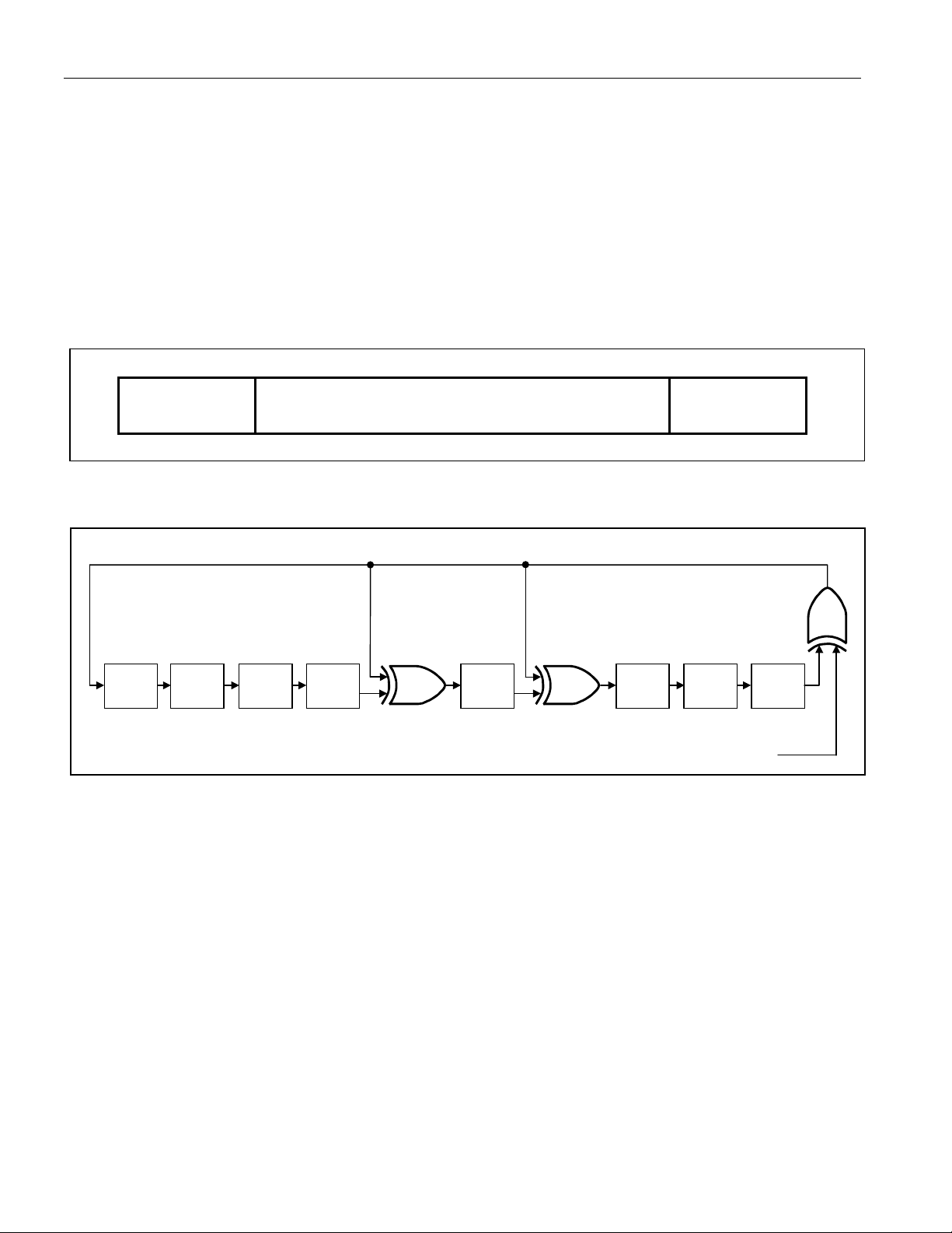
64 位光刻 ROM
每个 DS2431 都有唯一一个 64 位 ROM 代码,其中前 8 位是一个 1-Wire 家族码,中间 48 位是唯一的序列号,最后
8 位是前 56 位的 CRC(循环冗余校验)码。详见图 3 所示。1-Wire CRC 校验码通过一个包括移位寄存器和异或门
的多项式发生器产生,如图 4 所示。该多项式为:X
考
应用笔记
27。
8
+ X5 + X4 + 1。有关 Dallas 1-Wire CRC 校验码的更多信息请参
移位寄存器初始化时被清 0。然后从家族码的最低有效位开始,每次移入一位。当家族码的最后一位被移入后,再移
入序列号。当序列号的最后一位也被移入时,移位寄存器的值即为 CRC 码的值。继续移入 8 位 CRC 码后,移位寄
存器所有位归 0。
图 3. 64 位光刻 ROM
MSB LSB
8-Bit
CRC Code
48-Bit Serial Number
8-Bit Family
Code (2Dh)
MSB LSB MSB LSB MSB LSB
图 4. 1-Wire CRC 发生器
Polynomial = X8 + X5 + X4 + 1
STAGE
0
X
st
1
1
X
nd
2
STAGE
2
X
rd
3
STAGE
STAGE
3
X
th
4
STAGE
4
X
th
5
STAGE
5
X
th
6
STAGE
6
X
INPUT DATA
th
7
STAGE
7
X
th
8
8
X
6 of 24
Page 7

DS2431: 1024 位 1-Wire EEPROM
图 5.存储器映像
ADDRESS RANGE TYPE DESCRIPTION PROTECTION CODES
0000h to 001Fh R/(W) Data Memory Page 0
0020h to 003Fh R/(W) Data Memory Page 1
0040h to 005Fh R/(W) Data Memory Page 2
0060h to 007Fh R/(W) Data Memory Page 3
0080h1) R/(W) Protection Control Byte
Page 0
0081h1) R/(W) Protection Control Byte
Page 1
0082h1) R/(W) Protection Control Byte
Page 2
0083h1) R/(W) Protection Control Byte
Page 3
0084h1) R/(W) Copy Protection Byte 55h or AAh: Copy Protect 0080:008Fh, and
0085h R Factory byte. Set at
Factory.
0086h R/(W) User Byte/Manufacturer ID
0087h R/(W) User Byte/Manufacturer ID
0088h to 008Fh N/A Reserved
1)
一旦被设置为 AAh 或 55h,该地址将变为只读。可以被设为其它任意值,但不能对该地址起到写保护作用,也不激
活任何功能。
55h: Write Protect P0; AAh: EPROM mode
P0; 55h or AAh: Write Protect 80h
55h: Write Protect P1; AAh: EPROM mode
P1; 55h or AAh: Write Protect 81h
55h: Write Protect P2; AAh: EPROM mode
P2; 55h or AAh: Write Protect 82h
55h: Write Protect P3; AAh: EPROM mode
P3; 55h or AAh: Write Protect 83h
any write-protected Pages
AAh:Write Protect 85h, 86h, 87h;
55h: Write Protect 85h, unprotect 86h, 87h
存储器
数据存储器和寄存器位于一个线性地址空间,如图 5 所示。数据存储器和寄存器对读操作没有限制。DS2431 的
EEPROM 阵列共有 18 行,每行 8 字节。前 16 行被等分为 4 个存储器页(每页 32 字节),这 4 页为主数据存储
器。可以通过设置寄存器行中相应的保护字节将每一页单独设置成开放(无保护),写保护,或 EPROM 模式。最
后两行包括保护寄存器和保留字节。寄存器行包括 4 个保护控制字节,1 个复制保护字节,1 个工厂预置字节,和两
个用户/厂商 ID 字节。厂商 ID 可以是客户要求的标识码,用于帮助应用软件识别与 DS2431 有关的产品。要设置并
注册一个定制的厂商 ID 请与工厂联系。最后一行为将来的应用所保留。未定义读/写功能,不能使用这些操作。
除主 EEPROM 阵列之外,还包含一个 8 字节易失暂存器。向 EEPROM 阵列写入数据包括两个步骤。首先,数据先
写到暂存器,然后被复制到主存储器阵列。这就允许用户在将数据复制到主存储器阵列前先对数据进行校验。器件
仅支持整行(8 字节)复制操作。为保证复制操作中暂存器的数据有效,写暂存器命令提供的地址必须开始于一行的
边界处,而且暂存器必须写入 8 个完整的字节。
7 of 24
Page 8

DS2431: 1024 位 1-Wire EEPROM
保护控制寄存器决定执行写暂存器命令时输入数据如何被加载到暂存器。保护控制寄存器设置为 55h(写保护)时,
输入的数据被忽略,位于目标地址的主存储器数据被加载到暂存器。保护控制寄存器设置为 AAh(EPROM 模式)
时,输入数据与目标地址的主存储器数据进行逻辑与,计算结果被加载到暂存器。保护控制寄存器的其它任意设置
值使相关存储器页处于不限制写操作的开放状态。保护控制字节设置成 55h 或 AAh 时,该字节自身也受写保护。保
护控制字节设置成 55h 并不阻止复制操作。这就允许被写保护的数据在器件内部进行刷新(即用当前数据重新编
程)。
复制保护字节用于更高的安全级别,仅应在其它所有保护控制字节,用户字节,写保护页被设置成最终值后才被使
用。如果复制保护字节置为 55h 或 AAh,将阻止所有试图向寄存器行和用户字节行复制的操作。此外,所有试图向
写保护的主存储器页复制的操作(即刷新)也被阻止。
地址寄存器和传输状态
DS2431 使用 3 个地址寄存器:TA1,TA2,以及 E/S(见图 6)。这些寄存器在许多其它 1-Wire 器件中都很常见,但
用法与 DS2431 略有不同。寄存器 TA1 和 TA2 必须加载进行数据写入或读出的目标存储器地址。寄存器 E/S 是一个
只读的传输状态寄存器,用来校验写操作命令的输入数据完整性。ES 的 E2:E0 位加载写暂存器命令所输入的 T2:T0
位,每输入一个数据字节加 1。这实际上是一个 8 字节暂存器内部的字节结束偏移计数器。E/S 寄存器的第 5 位,称
作 PF,如果暂存器数据因掉电或主机发送的数据未能按要求填满整个暂存器而无效,该位被置为逻辑 1。为了使写
入暂存器数据有效,T2:T0 位必须为 0,而且主机必须发送完整 8 个字节数据。第 3,4,6 位没有定义功能;读数总
为 0。E/S 寄存器的最高位,称为 AA 或授权许可,作为指示暂存器数据已被复制到目标存储器地址的标志位,向暂
存器中写入数据将清除此位。
图 6. 地址寄存器
Bit # 7 6 5 4 3 2 1 0
Target Address (TA1) T7 T6 T5 T4 T3 T2 T1 T0
Target Address (TA2) T15 T14 T13 T12 T11 T10 T9 T8
Ending Address with
Data Status (E/S)
(Read Only)
AA 0 PF 0 0 E2 E1 E0
8 of 24
Page 9

DS2431: 1024 位 1-Wire EEPROM
带校验的写操作
向 DS2431 写入数据时,必须把暂存器用作中间存储器,首先主机发送 Write Scratchpad 命令并指定目标存储器地
址,随后发送要写入暂存器的数据。注意 Copy Scratchpad 命令必须在达到 8 字节边界时执行。也就是说,目标地
址的低 3 位(T2..T0)必须等于 000b。如果 T2..T0 是非 0 值,复制命令将被中止。在一定条件下(见 Write
Scratchpad 写暂存器命令),主机将接收到一个反码的 CRC16 校验码,用于校验命令、地址(实际发送的地址)
和位于 Write Scratchpad 命令序列末尾的数据。收到该 CRC 校验码后,主机与自己的计算结果进行比较,判断通信
是否成功,并决定是否继续执行 Copy Scratchpad 命令。如果主机没有接收到 CRC16 码,主机应发送一条 Read
Scratchpad 命令来验证数据的完整性。在回送暂存器数据前,DS2431 先发送目标地址 TA1 和 TA2,以及 E/S 寄存
器值。如果 PF 标志位置位,说明数据未能正确送达暂存器或者上一次写暂存器后发生过掉电故障。这样主机就无需
继续读入数据;可以重新开始向暂存器写入数据。类似地,如果 AA 标志位置位,同时 PF 标志位清零,则说明器件
未能认可写命令。如果一切正常,两个标志位均被清零。此时主机即可继续读取和验证每个数据字节了。主机完成
数据校验后,就可发送 Copy Scratchpad 命令了。此命令之后必须紧随三个地址寄存器中的数据,TA1,TA2 和
E/S。主机应通过读暂存器获知这些寄存器的内容。
存储器功能命令
存储器功能流程图(图 7)说明了访问 DS2431 存储器所需要的协议。本文档的最后给出了一个如何利用这些功能读
取和写入数据的示例。主机和 DS2431 之间可在标准速率(默认值,OD = 0)或高速模式(OD = 1)下通信。如没
有明确设置成高速模式,DS2431 默认以标准速率通信。
Write Scratchpad 命令 [0Fh]
Write Scratchpad 命令适用于数据存储器和寄存器页中的可写地址。为了保证暂存器中的数据能够被正确复制到存储
器阵列中,用户必须保证写暂存器命令中的 8 个数据字节开始于一个有效行边界处。Write Scratchpad 命令接受无效
地址和不完整的存储器行,但后续的 Copy Scratchpad 命令将被阻止。
发出 Write Scratchpad 命令后,主机必须首先发送 2 个字节的目标地址,接着发送要写入暂存器的数据。写入暂存
器的数据起始字节偏移量为 T2:T0。ES 的 E2:E0 位加载起始字节偏移量,后面每收到一个数据字节加 1。E2:E0 最
终结果为最后被写入暂存器的完整字节的偏移量。仅接受完整数据字节。
当执行 Write Scratchpad 命令时,DS2431 内部的 CRC 发生器(图 13)随着主机的发送过程,计算整个数据流的
CRC 校验码,始于命令代码,终止于最后一个数据字节。该 CRC 校验码由 CRC16 多项式生成,计算时首先清除
CRC 发生器,然后顺序移入 Write Scratchpad 命令代码(0Fh),目标地址(TA1 和 TA2),和所有数据字节。要
注意的是,CRC16 计算时使用的是由主机实际发送的 TA1、TA2 和数据字节。主机可在任意时间终止 Write
Scratchpad 命令。但如果写入数据达到暂存器上限(E2:E0 = 111b),主机可发送 16 个读时隙并收到 DS2431 产
生的 CRC 校验码。
如果 Write Scratchpad 命令试图对写保护区域进行写入,暂存器将加载存储器原有的数据,而不是主机发送的数
据。类似地,如果目标地址页为 EPROM 模式,暂存器加载的则是存储器原有数据与主机发送数据位逻辑与的结
果。
9 of 24
Page 10
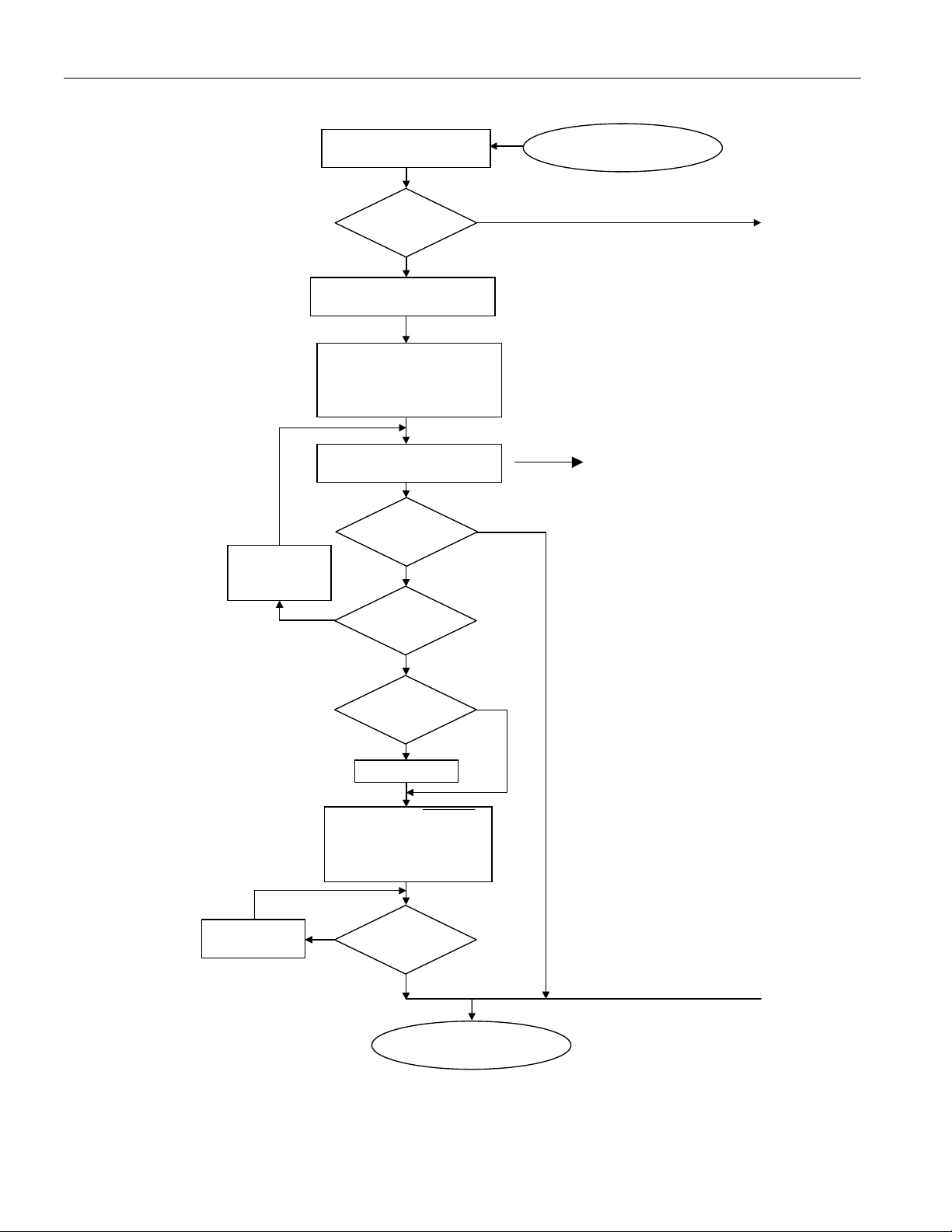
图 7-1. 存储器功能流程图
(
)
(Fig
)
(Fig
)
A
p
p
DS2431: 1024 位 1-Wire EEPROM
DS2431
Increments
E2:E0
Bus Master TX Memory
Function Command
0Fh
Write Scratch-
pad ?
Y
Bus Master TX
TA1
T7:T0), TA2 (T15:T8
DS2431 sets
Sets PF = 1
Clears AA = 0
Sets E2:E0 = T2:T0
Master TX Data Byte
N
To Scratch
Master
TX Reset ?
E2:E0
= 7 ?
T2:T0
= 0 ?
PF = 0
ad
N
Y
Y
From ROM Functions
Flow Chart
N
pplies only if the
memory area is not
rotected.
Y
N
If
write-protected
the DS2431 copies the
data byte from the target address into the SP.
If in
then the DS2431 loads
the bitwise logical AND
of the transmitted byte
and the data byte from
the targeted address
into the SP.
ure 9
To Figure 7
nd
2
Part
EPROM mode
, then
,
DS2431 TX CRC16
of Command, Address,
Data Bytes as they were
sent by the bus master
Bus Master
RX “1”s
N
Master
TX Reset ?
Y
To ROM Functions
Flow Chart
ure 9
From Figure 7
nd
2
Part
10 of 24
Page 11

图 7-2. 存储器功能流程图(续)
y
y
y
y
y
r
DS2431: 1024 位 1-Wire EEPROM
From Figure 7
st
1
Part
DS2431
Increments
te Counte
B
AAh
Read Scratch-
Pad ?
Y
Bus Master RX
TA1 (T7:T0), TA2 (T15:T8)
and E/S B
te
DS2431 sets Scratchpad
te Counter = T2:T0
B
Bus Master RX
Data B
te from Scratchpad
Master
Y
TX Reset ?
N
N
Byte Counter
= E2:E0 ?
To Figure 7
N
3
rd
Part
To Figure 7
st
1
Part
Bus Master
RX “1”s
Y
Bus Master RX CRC16
of Command, Address,
E/S Byte, Data Bytes as
the DS2431
sent b
N
Master
TX Reset ?
Y
From Figure 7
rd
3
Part
11 of 24
Page 12
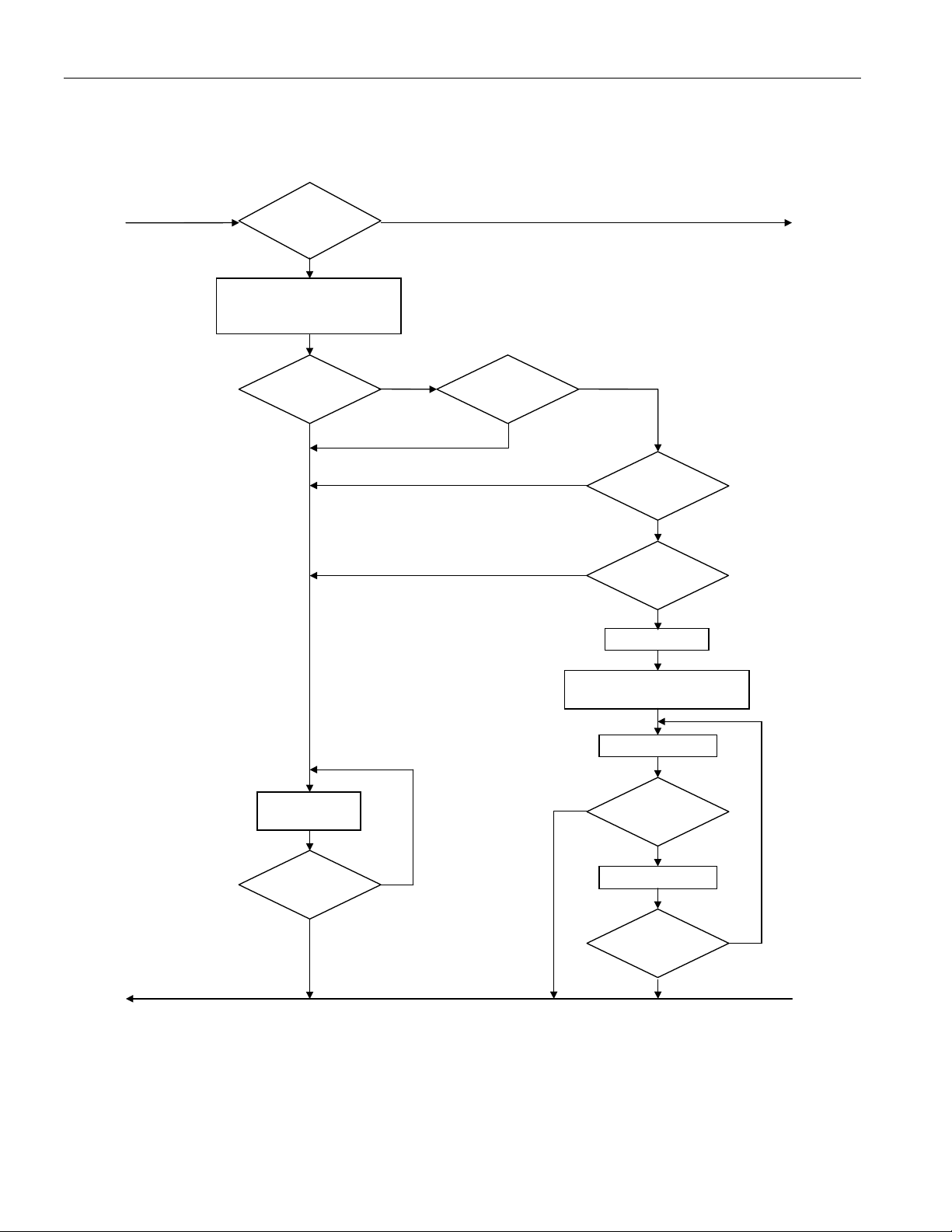
图 7-3. 存储器功能流程图(续)
y
p
A
DS2431: 1024 位 1-Wire EEPROM
From Figure 7
nd
2
Part
TA1 (T7:T0), TA2 (T15:T8)
55h
Copy Scratch-
Pad ?
Y
Bus Master TX
and E/S B
te
Auth. Code
Match ?
N
To Figure 7
N
4
th
Part
pplicable to all R/W
memory locations.
Y
T15:T0
Y
< 0090h ?
N
N
PF = 0 ?
Y
Y
Copy-
Protected ?
N
AA = 1
Bus Master
RX “1”s
Master
N
TX Reset ?
Y
To Figure 7
nd
2
Part
* 1-Wire idle high for power
12 of 24
DS2431 copies Scratch-
ad Data to Address
DS2431 TX “0”
Y
Master
TX Reset ?
N
DS2431 TX “1”
Master
TX Reset ?
Y
From Figure 7
th
4
Part
*
N
Page 13

图 7-4. 存储器功能流程图(续)
(
)
(
)
r
y
From Figure 7
3
rd
Part
F0h
Read Memory ?
Y
Bus Master TX
TA1 (T7:T0),
TA2
T15:T8
DS2431: 1024 位 1-Wire EEPROM
N
Address
< 90h ?
N
DS2431
Increments
Address
Y
Counte
DS2431 sets Memory
Address =
Bus Master RX
Data Byte from
Memor
TX Reset ?
Y
T15:T0
Address
Master
N
Address
< 8Fh ?
N
Y
Bus Master
RX “1”s
Bus Master
RX “1”s
To Figure 7
rd
3
Part
13 of 24
N
Master
TX Reset ?
Y
N
Master
TX Reset ?
Y
Page 14

DS2431: 1024 位 1-Wire EEPROM
Read Scratchpad 命令[AAh]
Read Scratchpad 命令可以用来校验目标地址和暂存器数据的完整性。主机发送命令代码后开始读取数据。开头的两
个字节是目标地址,下一个字节是结束偏移量/数据状态字节(E/S),接着是暂存器数据,这些数据可能与主机发送
的原始数据有所不同。当目标地址位于寄存器页或位于写保护或 EPROM 模式页时,这一点尤其重要。详细信息见
Write Scratchpad 命令说明。主机应先读完暂存器中所有数据(E2:E0 - T2:T0 + 1 个字节),然后就可以收到反码
的 CRC,该 CRC 码根据 DS2431 发送的数据产生。如果主机在收到 CRC 码后继续读取数据,得到的所有数据均为
逻辑 1。
Copy Scratchpad [55h]
Copy Scratchpad 命令用来将暂存器中的数据复制到可写的存储器区域,发出 Copy Scratchpad 命令后,主机必须
提供一个 3 字节的授权模式,该数据应该通过紧邻此条命令的前一个 Read Scratchpad 命令获得。该 3 字节模式数
据必须与三个地址寄存器(依次为 TA1,TA2,E/S)中的数据正确匹配。如果授权码匹配,目标地址有效,PF 标
志位未被置位,目标存储器没有复制保护,AA(授权许可)标志位置位,才能开始执行复制操作。暂存器中的 8 字
节数据全部被复制到目标存储器。器件的内部数据传输需要最多 13 毫秒,在此期间 1-Wire 总线上的电压必须保证
不低于 2.8V。数据复制完成后会发送一组“0”和“1”交替的信号,直到主机发送复位脉冲为止。如果 PF 标志位被置位
或目标存储器处于复制保护模式,则不会执行复制操作而且 AA 标志位不会置位。
Read Memory [F0h]
Read Memory 命令通常用于从 DS2431 读取数据。发出命令后,主机需要提供 2 个字节的目标地址。在这两个字节
之后,主机开始读取始于目标地址的数据,可连续读至地址 008Fh 处。如果继续读,读取结果将是逻辑 1。器件内
部的 TA1,TA2,E/S,以及暂存器内容不受 Read Memory 命令影响。
1-Wire 总线系统
1-Wire 单总线系统是用一根数据线连接单个主机和一台或多台从机设备的系统。在所有的情况下,DS2431 都只能
作为从机设备来使用。总线上主机是一个典型的微控制器。关于单总线系统的讨论分为三个部分:硬件配置,处理
流程,和 1-Wire 信令(信号类型和时序)。1-Wire 协议规定总线的收发按照特殊时隙下的总线状态进行,由主机发
出的同步脉冲下降沿初始化。
硬件配置
1-Wire 总线只定义了一根数据线;因此总线上的每个设备在适当时刻能够驱动总线是非常重要的。为了实现此目
的,挂接在 1-Wire 总线上的所有设备都必须采用漏极开路或三态输出。DS2431 的 1-Wire 端口为漏极开路,内部等
效电路见图 8。
多点总线由连接了多个从机设备的 1-Wire 总线组成。DS2431 分别支持 15.4kbps (max)的标准通信速率和
111kbps(max)的高速通信速率。注意传统的 1-Wire 产品分别支持 16.3kbps 的标准通信速率和 142kbps 的高速通
信速率。DS2431 速率略有降低,原因是为增强 1-Wire 物理接口对噪声的抑制而增加了恢复时间。上拉电阻的阻值
主要由网络的大小和负载条件决定。DS2431 在任何速度下运行都需要一个 2.2kΩ(max)的上拉电阻。
1-Wire 总线的空闲状态为高电平。如果由于某种原因需暂停通信,若还需要恢复通信的话,总线必须保持在空闲状
态。如果未设置为空闲状态,在高速模式,总线处于低电平时间超过 16µs,标准速率模式超过 120µs,总线上的一
个或多个器件将被复位。
14 of 24
Page 15

图 8. 硬件配置
BUS MASTER DS2431 1-Wire PORT
DS2431: 1024 位 1-Wire EEPROM
V
PUP
R
PUP
RX
2.2µA
TX
Open Drain
Port Pin
RX = RECEIVE
TX = TRANSMIT
Max.
100
MOSFET
RXDATA
TX
Ω
处理流程
通过 1-Wire 端口访问 DS2431 的协议如下:
初始化
ROM 功能指令
存储器功能指令
传输/数据
初始化
所有 1-Wire 总线上的数据传输都以初始化过程开始。初始化过程包括主机发送一个复位脉冲,各从机随后发送应答
脉冲。应答脉冲让主机得知 DS2431 在线并且准备就绪。更多信息请参阅 1-Wire
信令
一节。
1-Wire ROM 功能命令
一旦主机检测得到一个应答脉冲,便可发送 DS2431 支持的七条 ROM 功能命令中的任一条。所有的 ROM 功能命令
长度均为 8 位。下面列出了所有的 ROM 命令(参考图 9 中的流程图)。
Read ROM [33h]
此命令允许主机读取 DS2431 的 8 位家族码,唯一的 48 位序列号和 8 位 CRC 校验码。此命令适用于总线上仅有一
个从机的情况。如果总线上连接了多个从机设备,当所有从机试图同时发送数据时,将会发生数据冲突(漏极开路
输出产生一个线与的结果)。导致主机收到的家族码和 48 位序列号与 CRC 校验码不匹配。
Match ROM [55h]
Match ROM 命令后面跟随一个 64 位 ROM 地址码,允许主机访问多点总线上的一个特定 DS2431。只有与该 64 位
ROM 地址码正确匹配的 DS2431 才会对后面的存储器功能命令做出反应。其它所有从机均等待下一个复位脉冲。这
条命令既适用于单从机系统,也适用于多从机系统。
15 of 24
Page 16

DS2431: 1024 位 1-Wire EEPROM
Search ROM [F0h]
系统刚启动时,主机可能并不知道多少设备挂在 1-Wire 总线上,也不知道它们具体的地址码。主机可利用总线上的
线与特性,采用排除法来识别总线上所有从机的地址码。先发送地址码的最低有效位,主机针对每一位都发送三个
时隙。第一个时隙,每个参与搜索的从机都输出各自地址码该位的值。第二个时隙,每个参与搜索的从机都输出该
位的补码。第三个时隙,主机写入该位指定值。所有与该值不匹配的从机都不再参加搜索。如果主机两次读到的值
均是 0,则说明从机该位的两个状态都存在。主机通过写入的状态值来选择搜索 ROM 码树的不同分支。经过一次完
整搜索过程,主机即可知道某个从机的地址码。另外的搜索过程可以识别其余从机的地址码。详细讨论请参考
笔记
187:1-Wire
搜索算法
,其中包括一个示例。
应用
Skip ROM [CCh]
在一个单从机总线系统中,主机可使用此命令访问存储器而不需要提供 64 位 ROM 地址码,从而节省时间。如果总
线上不止一个从机,当一条 Read 命令紧跟一条 Skip ROM 命令发送时,会因多个从机同时发送数据而导致数据冲
突。(漏极开路输出下拉将产生一个线与结果)。
Resume [A5h]
为了最大程度提高多点环境中的数据吞吐率,系统提供了 Resume 功能。此功能检查 RC 位的状态,如果置位,则
直接把控制权交给存储器功能,与 Skip ROM 命令类似。RC 的置位只能通过成功地执行 Match ROM、Search
ROM 或 Overdrive Match ROM 命令来实现。一旦 RC 置位,即可利用 Resume 命令重复访问此器件。访问总线上
的其它器件会清除 RC 位,以防止两个或更多的从机同时响应 Resume 命令。
Overdrive Skip ROM [3Ch]
在一个单从机总线上使用该命令时,主机不需要提供 64 位的 ROM 地址码就可以访问存贮器功能,从而节省了时
间。与通常的 Skip ROM 命令不同,Overdrive Skip ROM 命令将 DS2431 设置为高速模式(OD = 1)。该命令后的
所有通信均为高速模式,直到有一个最短持续 480µs 时间的复位脉冲将总线上的所有器件复位成标准速率(OD =
0)。
如果在一个多点总线上发送该命令,则总线上所有支持高速模式的器件都被设置成高速模式。随后,为了寻址特定
的高速模式器件,必须发出一个高速模式的复位脉冲,接着运用 Match ROM 或 Search ROM 命令。这样能够加速
搜索过程。如果总线上有多个支持高速模式的从机,而且 Overdrive Skip ROM 命令后跟着一条 Read 命令,会因多
个从机同时发送数据而产生数据冲突(漏极开路输出下拉将产生一个线与结果)。
Overdrive Match ROM [69h]
通过 Overdrive Match ROM 命令,后接以高速模式发送的 64 位 ROM 地址码,能够使总线主机在多点总线上访问一
个特定的 DS2431,同时将其设置成高速模式。只有与该 64 位 ROM 地址码正确匹配的 DS2431 才会对后续的存储
器功能命令做出反应。已经被前面的 Overdrive Skip 或 Overdrive Match 命令成功设置成高速模式的从机将继续保持
高速模式。所有支持高速模式的从机在下一个持续时间最小为 480µs 的复位脉冲后回到标准速率。Overdrive Match
ROM 命令适用于总线上有单个或多个器件的情况。
16 of 24
Page 17

图 9-1. ROM 功能流程图
(Fig
)
y
(Fig
)
From Memory Functions
Flow Chart
ure 7
Bus Master TX
Reset Pulse
OD
Reset Pulse ?
Y
DS2431: 1024 位 1-Wire EEPROM
From Figure 9, 2ndPart
N
OD = 0
Bus Master TX ROM
Function Command
33h
Read ROM
Command ?
RC = 0
DS2431 TX
Family Code
(1 Byte)
DS2431 TX
Serial Number
(6 Bytes)
DS2431 TX
Presence Pulse
To Figure 9
N
55h
Match ROM
Command ?
RC = 0
Master TX Bit 0
Bit 0
Match ?
Master TX Bit 1
Bit 1
Match ?
N
N
N
Y
N
N
Y
F0h
Search ROM
Command ?
YY YY
RC = 0
DS2431 TX Bit 0
DS2431 TX Bit 0
Master TX Bit 0
Bit 0
Match ?
Y
DS2431 TX Bit 1
DS2431 TX Bit 1
Master TX Bit 1
Bit 1
Match ?
Y
N
CCh
Skip ROM
Command ?
RC = 0
nd
2
Part
N
DS2431 TX
CRC B
te
Master TX Bit 63
Bit 63
Match ?
Y
RC = 1
N
To Memory Functions
Flow Chart
17 of 24
DS2431 TX Bit 63
DS2431 TX Bit 63
Master TX Bit 63
N
Bit 63
Match ?
RC = 1
ure 7
Y
To Figure 9
nd
2
Part
From Figure 9
nd
2
Part
Page 18

图 9-2. ROM 功能流程图(续)
To Figure 9, 1st Part
From Figure 9
1
st
Part
A5h
Resume
Command ?
DS2431: 1024 位 1-Wire EEPROM
N
3Ch
Overdrive
Skip ROM ?
N
69h
Overdrive Match
ROM ?
N
From Figure 9
st
1
Part
RC = 1 ?
Y
Y
N
Master
TX Reset ?
N
Y
RC = 0 ; OD = 1
Master
TX Reset ?
N
Y
Y
RC = 0 ; OD = 1
Master TX Bit 0
Y
Bit 0
Match ?
Master TX Bit 1
Bit 1
Match ?
Master TX Bit 63
Bit 63
Match ?
RC = 1
N
OD = 0
Y
N
OD = 0
Y
N
OD = 0
Y
To Figure 9
st
1
Part
18 of 24
Page 19

DS2431: 1024 位 1-Wire EEPROM
ε
1-Wire 信令
DS2431 需要严格的协议来保证数据完整性。该协议在一根线上定义了四种类型的信号:包括复位脉冲和应答脉冲的
复位序列,写 0,写 1,和读数据。除应答脉冲外,总线主机发出所有其它信号的下降沿。DS2431 能以标准速度或
高速两种模式通信。如果没有明确设置为高速模式,DS2431 就以标准速度通信。在高速模式下,所有波形均采用快
速定时。
当从空闲状态被激活时,1-Wire 线上的电压需要从 V
需要从 V
(R
)和 1-Wire 网络的附加电容。电压 V
PUP
上升至门限电压 VTH以上。电压上升时间见图 10 所示的“ε”,其持续时间取决于使用的上拉电阻
ILMAX
在 DS2431 判断逻辑电平时,与其有关,且不会触发任何事件。
ILMAX
降到门限电压 VTL以下。要从活动状态返回空闲状态,电压
PUP
启动与 DS2431 的任何通信都需要初始化过程,见图 10。复位脉冲后的应答脉冲,表明 DS2431 已经准备就绪,只
要收到正确的 ROM 和存储器功能命令,即可接收数据。 如果主机在下降沿采用摆率控制,作为补偿,需要将线上
的电平拉低并保持 t
RSTL +tF
DS2431 处于高速模式并且 t
的时间。高速模式下若 t
不大于 80µs,则其仍保持高速模式。
RSTL
持续 480µs 或更长时,可将从机恢复到标准速度。如果
RSTL
图 10. 初始化过程:复位和应答脉冲
V
PUP
V
IHMASTER
V
TH
V
TL
V
ILMAX
0V
MASTER TX “RESET PULSE” MASTER RX “PRESENCE PULSE”
t
MSP
t
F
t
RSTL
t
PDH
t
PDL
t
RSTH
t
REC
RESISTOR MASTER DS2431
主机释放总线后进入接收模式。此时 1-Wire 总线电平被上拉电阻,或 DS2482-x00、DS2480B 驱动器等有源电路上
拉至 V
脉冲。为了检测应答脉冲,主机必须在 t
。当电平高于门限 VTH时,DS2431 等待 t
PUP
时间检测 1-Wire 总线的逻辑电平。
MSP
时间,然后通过将总线电平拉低并保持 t
PDH
,来发送一个应答
PDL
t
窗口时间必须至少等于 t
RSTH
个混和设备组成的网络中,为了兼容其它 1-Wire 设备, t
PDHMAX
, t
PDLMAX
, 与 t
的总和。一旦 t
RECMIN
结束,DS2431 即可开始数据通信。在一
RSTH
在标准速度下最小应为 480µs,在高速模式下最小应为
RSTH
48µs。
读/写时隙
与 DS2431 的数据通信在时隙内进行,每时隙传输一位。数据在写时隙由主机传输到从机。数据在读时隙由从机传
输到主机。图 11 说明了读时隙和写时隙的定义。
所有通信均以主机拉低数据线开始,当 1-Wire 总线上的电压降至门限电压 V
器,在写时隙时确定何时采样数据线,在读时隙时确定数据有效的时间。
以下时,DS2431 启动内部定时发生
TL
19 of 24
Page 20

主机到从机
对于“写 1”时隙,数据线上的电压必须在“写 1”低时间 t
电压在“写 0”低时间 t
或 t
t
时间窗口内都不应超过 V
W1L
。
REC
结束前必须保持低于门限电压 VTH。为了实现最可靠的通信,数据线上的电压在整个 t
W0LMIN
。数据线上的电压超过 VTH后, DS2431 在进行下一个时隙前需要一个恢复时间
ILMAX
图 11. 读/写时序图
Write-One Time Slot
t
W1L
ε
V
IHMASTER
V
V
PUP
V
V
ILMAX
0V
TH
TL
t
F
结束前高过门限电压 V
W1LMAX
t
SLOT
DS2431: 1024 位 1-Wire EEPROM
。对于“写 0”时隙,数据线上的
TH
W0L
Write-Zero Time Slot
V
PUP
V
IHMASTER
V
TH
V
TL
V
ILMAX
0V
Read-Data Time Slot
V
PUP
V
IHMASTER
V
TH
V
TL
V
ILMAX
0V
RESISTOR MASTER
t
W0L
t
F
t
RESISTOR MASTER
t
t
RL
MSR
Master
Sampling
Window
t
F
δ
SLOT
t
SLOT
t
REC
t
REC
RESISTOR MASTER DS2431
20 of 24
Page 21

DS2431: 1024 位 1-Wire EEPROM
从机到主机
“读数据”时隙在开始时与“写 1”时隙类似。数据线上的电压在读低时间 t
答 0 时,DS2431 开始拉低数据线;其内部定时发生器决定何时结束下拉,电平重新开始升高。应答 1 时,DS2431
并不保持数据线的低电平,t
一结束,电平即开始上升。
RL
主机采样窗口(t
MSRMIN
到 t
)一方面由 tRL+δ(上升时间),另一方面由 DS2431 内部定时发生器决定,主机
MSRMAX
必须在采样窗口内执行一次数据线读操作。为实现最可靠的通信,t
晚于 t
准备就绪前有足够的恢复时间 t
的时间读取数据。从数据线读取数据后,主机必须等待直至 t
MSRMAX
。需注意的是,这里指定的 t
REC
REC
况。在一个多点总线上,为了适应其它 1-Wire 器件的输入电容,应延长 t
DS2480B 等 1-Wire 总线驱动器接口器件,在 1-Wire 恢复时间内进行有源上拉。
结束前必须保持低于 VTL。在 tRL窗口,应
RL
在允许范围内应尽量短,主机应该在接近但不
RL
结束。这确保了 DS2431 在下一个时隙
SLOT
仅适用于 1-Wire 总线上只接一个 DS2431 的情
。另外,还可使用 DS2482-x00 或
REC
改善的网络性能(切换点滞回)
在 1-Wire 环境中,线路端接只有在总线主机(1-Wire 驱动器)控制的短时间内才有可能。因此,1-Wire 网络极易受
到各种来源的噪声干扰。由于网络的大小和拓扑结构不同,从端点或支路节点反射的信号可能在某种程度上相互加
强或抵消。这些反射信号在 1-Wire 通信线路上看来象毛刺或振铃。从外部耦合到 1-Wire 线路上的噪声也能导致信号
产生毛刺。在一个时隙上升沿产生的毛刺会导致从机与主机失去同步,继而导致对 search ROM 命令失去反应,或
导致从机执行特定功能命令失败。为了实现更好的网络性能,DS2431 使用了一种新的 1-Wire 前端,降低了其对噪
声的敏感度,同时也降低了其自身引入到 1-Wire 总线的噪声幅度。
DS2431 的 1-Wire 前端与传统的从机器件相比有 4 点特性不同。
1)应答脉冲下降沿摆率可控。可提供比数字开关晶体管更好的线路阻抗匹配,从而改善传统器件出现的高频振铃,
使之成为更平滑的低带宽转换。摆率控制由参数 t
表示,该参数的值在标准速度和高速模式下不同。
FPD
2)在电路中附加了一个低通滤波器来检测时隙开始时的下降沿。这降低了对高频噪声的敏感度。高速模式下不使用
此附加滤波器。
3)在低到高的开关门限 V
处设有一个滞回,如果有一个负毛刺低于 VTH但还没有低于 V
TH
- VHY,将不会被承认
TH
(图 12,示例 A),滞回在任何 1-Wire 速度模式下均有效。
4)由上升沿保持关闭时间 t
示例 B,t
GL
< t
)。大的压降或穿过 VTH门限后延续时间超出 t
REH
隙的开始(图 12,示例 C,t
只有在电气特性中指明参数 t
定义了一个时间窗口,在该时间窗口内即使毛刺低于 V
REH
窗口的毛刺则无法滤除,会被当作一个新时
REH
≥ t
REH
和 t
)。
的器件使用了改进的 1-Wire 前端。
REH
GL
FPD,VHY
- VHY也会被忽略(图 12,
TH
图 12. 噪声抑制示意图
V
PUP
t
REH
t
REH
V
TH
V
HY
Case A Case CCase B
0V
t
GL
21 of 24
t
GL
Page 22

DS2431: 1024 位 1-Wire EEPROM
A
生成 CRC 码
DS2431 有两种不同类型的 CRC 码。一种为 8 位,存储在 64 位 ROM 的最高字节中。主机能根据 64 位 ROM 码的
前 56 位计算出该 CRC 码,并与存储在 DS2431 中的值比较,判断 ROM 数据是否接收无误。计算该 CRC 校验码的
等效多项式为:X
8
+ X5 + X4 + 1。接收到的 8 位 CRC 为原码(不取反)形式。该值在工厂计算并被光刻写入 ROM
中。
另一种 CRC 码为 16 位,采用标准的 CRC16 多项式函数 X
16
15
+ X
+ X2 + 1 产生。该 CRC 校验码用来对读写暂存器
时传输的数据进行快速校验。与 8 位 CRC 校验码不同,16 位 CRC 校验码总是以反码的形式传输。DS2431 芯片内
部的 CRC 发生器(见图 13)计算一个新的 16 位 CRC 校验码,如命令流程图(图 7)所示。主机通过比较由从机
读取的 CRC 校验码与利用接收数据计算出的 CRC 校验码,据此来决定是继续某一操作还是重新读取 CRC 码有误的
数据部分。
在 Write Scratchpad 命令中,首先清空 CRC 发生器,然后移入命令代码,目标地址 TA1 和 TA2,以及主机发送的
所有数据字节。DS2431 只有在 E2:E0 = 111b 时才发送 CRC 校验码。
在 Read Scratchpad 命令中,首先清空 CRC 发生器,然后移入命令代码,目标地址 TA1 和 TA2,E/S 字节,以及
DS2431 发送的暂存器数据。DS2431 只有在连续读取暂存器数据直到结尾时才发送 CRC 校验码。有关生成 CRC 校
验码的更多信息参考
应用笔记
27。
图 13. CRC-16 硬件说明及多项式
Polynomial = X16+ X15+ X2+ 1
STAGE
0
X
STAthGE
8
X
st
1
9
STAGE
1
X
STAGE
9
X
2
10
nd
th
11
th
STAGE
10
X
11
X
STAGE
2
X
th
12
STAGE
3
rd
X
3
X
13
STAGE
12
STAGE
指令细节 1-Wire 通信协议颜色编码
Master to slave Slave to master Programming
th
4
th
5
STAGE
4
X
th
14
th
STAGE
13
X
14
X
STAGE
5
X
th
15
STAGE
th
6
STAGE
6
X
th
7
th
8
STAGE
7
X
th
16
STAGE
15
X
16
X
CRC
OUTPUT
INPUT DAT
22 of 24
Page 23

命令细节 1-Wire 通信协议——符号表
符号 说 明
RST
PD
Select
WS
RS
CPS
RM
TA
TA-E/S
<8 – T2:T0 bytes>
<data to EOM>
CRC16\
FF loop
AA loop
Programming
由 1-Wire 主机产生的复位脉冲。
由 1-Wire 从机产生的应答脉冲。
满足 ROM 功能协议的命令和数据。
“Write Scratchpad”命令。
“Read Scratchpad”命令。
“Copy Scratchpad”命令。
“Read Memory”命令。
目标地址 TA1,TA2。
目标地址 TA1,TA2,以及 E/S 字节。
对于指定目标地址,传送到达暂存器末端所需的足够字节。
传送到达存储器末端所需的足够字节。
传送反码的 CRC16 校验码。
主机读取 FF 字节的不确定循环。
主机读取 AA 字节的不确定循环。
数据写入 EEPROM;在此期间 1-Wire 总线上不允许有任何活动。
写暂存器(不能失败)
DS2431: 1024 位 1-Wire EEPROM
RST PD Select WS TA <8 – T2:T0 bytes> CRC16\ FF loop
读暂存器(不能失败)
RST PD Select RS TA-E/S <8 – T2:T0 bytes> CRC16\ FF loop
复制暂存器(成功)
RST PD Select CPS TA-E/S Programming AA loop
复制暂存器(地址无效,PF = 1,或复制保护)
RST PD Select CPS TA-E/S FF loop
读存储器(成功)
RST PD Select RM TA <data to EOM> FF loop
读存储器(地址无效)
RST PD Select RM TA FF loop
23 of 24
Page 24

DS2431: 1024 位 1-Wire EEPROM
存储器功能示例
写入存储器第 1 页的前 8 个字节。读整个存储器。
总线上只有单个 DS2431 与主机连接,通信过程如下所示:
主机模式 数据(最低有效位优先) 说 明
TX (Reset)
RX (Presence)
TX CCh
TX 0Fh
TX 20h
TX 00h
TX <8 data bytes>
RX <2 bytes CRC16\>
TX (Reset)
RX (Presence)
TX CCh
TX AAh
RX 20h
RX 00h
RX 07h
RX <8 data bytes>
RX <2 bytes CRC16\>
TX (Reset)
RX (Presence)
TX CCh
TX 55h
复位脉冲
应答脉冲
发送“Skip ROM”命令
发送“Write Scratchpad”命令
TA1,起始偏移 = 20h
TA2,地址 = 00
20h
向暂存器写 8 字节数据
读 CRC 码检查数据完整性
复位脉冲
应答脉冲
发送“Skip ROM”命令
发送“Read Scratchpad”命令
读 TA1,起始偏移 = 20h
读 TA2,地址 = 00
20h
读 E/S,结束偏移 = 111b,AA,PF = 0
读暂存器数据并校验
读 CRC 码检查数据完整性
复位脉冲
应答脉冲
发送“Skip ROM”命令
发送“Copy Scratchpad”命令
TX 20h TA1
TX 00h
TA2 (授权码)
TX 07h E/S
---- <1-Wire idle high>
RX AAh
TX (Reset)
RX (Presence)
TX CCh
TX F0h
TX 00h
TX 00h
RX <144 data bytes>
TX (Reset)
RX (Presence)
等待 12.5 毫秒,保证复制所需的操作时间
读复制状态,AAh = 成功
复位脉冲
应答脉冲
发送“Skip ROM”命令
发送“Read Memory”命令
TA1,起始偏移 = 00h
TA2,地址 = 00
00h
读存储器全部数据
复位脉冲
应答脉冲
封装信息
(本数据资料的封装图未能反映最新的封装信息,有关封装的最新资料,请访问www.maxim-ic.com.cn/DallasPackInfo。)
24 of 24
Maxim /Dallas Semiconductor不对Maxim
Maxim Integrated Products, 120 San Gabriel D rive, Sunnyvale, CA 94086 408-737-7600
Maxim 标志是 Maxim Integrated Products, Inc.的注册商标。Dallas 标志是 Dallas Semiconductor Corp.的注册商标
产品以外的任何电路使用负责,也不提供其专利许可。
© 2004 Maxim Integrated Products, Inc. All rights reserved.
Maxim
保留在任何时间、没有任何通报的前提下修改产品资料和规格的权利。
。
 Loading...