

Page 1
www.maxim-ic.com
DS2430A
256-Bit 1-Wire EEPROM
FEATURES
256-bit Electrically Erasable Programmable
Read Only Memory (EEPROM) plus 64-bit
one-time programmable application register
Unique, factory-lasered and tested 64-bit
registration number (8-bit family code + 48-bit
serial number + 8-bit CRC tester) assures
absolute identity because no two parts are alike
Built-in multidrop controller ensures
compatibility with other MicroLAN products
EEPROM organized as one page of 32 bytes
for random access
Reduces control, address, data, and power to a
single data pin
Directly connects to a single port pin of a
microprocessor and communicates at up to
16.3kbits per second
8-bit family code specifies DS2430A
communication requirements to reader
Presence detector acknowledges when reader
first applies voltage
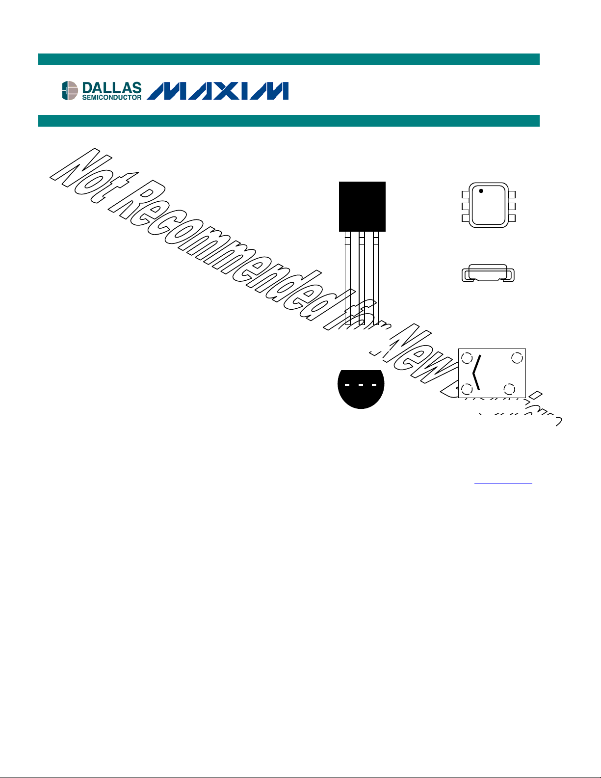
Low cost TO-92 or 6-pin TSOC and Flip Chip
surface mount package
Reads and writes over a wide voltage range of
2.8V to 6.0V from -40°C to +85°C
ORDERING INFORMATION
DS2430A TO-92 Package
DS2430AP 6-pin TSOC Package
DS2430A/T&R TO-92 Package, Tape & Reel
DS2430AP/T&R TSOC Package, Tape & Reel
DS2430A+ TO-92 Package
DS2430AP+ 6-pin TSOC Package
DS2430A+T&R TO-92 Package, Tape & Reel
DS2430AP+T&R TSOC Package, Tape & Reel
DS2430AX Flip Chip, 10k Tape & Reel
DS2430AX-S Flip Chip, 2.5k Tape & Reel
+ Indicates lead-free compliance.
PIN ASSIGNMENT
TO-92
DALLAS
DS2430A
1 2 3
2 3
BOTTOM VIEW
See Mech.
Drawings Section
TSOC PACKAGE
1
6
2
5
3
4
TOP VIEW
3.7mm x 4.0mm x 1.5mm
SIDE VIEW
See Mech.
Drawing Section
4 3
2430A
rrd#xx
1 2
Flip Chip, Top View
with Laser Mark,
Contacts Not Visible.
“rrd” = Revision/Date
#xx = Lot Number
See 56-G7016-001 for
package outline.
PIN DESCRIPTION
TO-92 TSOC Flip Chip
Pin 1 Ground Ground Ground
Pin 2 Data Data Data
Pin 3 NC NC NC
Pin 4 –––– NC NC
Pin 5 –––– NC ––––
Pin 6 –––– NC ––––
1 of 16 011607
Page 2

DS2430A
DESCRIPTION
The DS2430A 256-bit 1-Wire EEPROM identifies and stores relevant information about the product to
which it is associated. This lot or product specific information can be accessed with minimal interface, for
example a single port pin of a microcontroller. The DS2430A consists of a factory-lasered registration
number that includes a unique 48-bit serial number, an 8-bit CRC, and an 8-bit Family Code (14h) plus
256 bits of user-programmable EEPROM and a 64-bit one-time programmable application register. The
power to read and write the DS2430A is derived entirely from the 1-Wire® communication line. Data is
transferred serially via the 1-Wire protocol, which requires only a single data lead and a ground return.
The 48-bit serial number that is factory-lasered into each DS2430A provides a guaranteed unique identity
that allows for absolute traceability. The TO-92 and TSOC packages provide a compact enclosure that
allows standard assembly equipment to handle the device easily for attachment to printed circuit boards
or wiring. Typical applications include storage of calibration constants, board identification, and product
revision status.
OVERVIEW
The block diagram in Figure 1 shows the relationships between the major control and memory sections of
the DS2430A. The DS2430A has four main data components: 1) 64-bit lasered ROM, 2) 256-bit
EEPROM data memory with scratchpad, 3) 64-bit one-time programmable application register with
scratchpad and 4) 8-bit status memory. The hierarchical structure of the 1-Wire protocol is shown in
Figure 2. The bus master must first provide one of the four ROM Function Commands: 1) Read ROM, 2)
Match ROM, 3) Search ROM, 4) Skip ROM. The protocol required for these ROM Function Commands
is described in Figure 8. After a ROM Function Command is successfully executed, the memory
functions become accessible and the master can provide any one of the four memory function commands.
The protocol for these memory function commands is described in Figure 6. All data is read and written
least significant bit first.
64-BIT LASERED ROM
Each DS2430A contains a unique ROM code that is 64 bits long. The first 8 bits are a 1-Wire family code
(14h). The next 48 bits are a unique serial number. The last 8 bits are a CRC of the first 56 bits. (Figure
3). The 1-Wire CRC is generated using a polynomial generator consisting of a shift register and XOR
gates as shown in Figure 4. The polynomial is X8 + X5 + X4 + 1. Additional information about the Dallas
1-Wire Cyclic Redundancy Check is available in Application Note 27. The shift register bits are
initialized to 0. Then starting with the least significant bit of the family code, one bit at a time is shifted
in. After the 8th bit of the family code has been entered, then the serial number is entered. After the 48th
bit of the serial number has been entered, the shift register contains the CRC value. Shifting in the 8 bits
of CRC should return the shift register to all 0s.
1-Wire and iButton are registered trademarks of Dallas Semiconductor.
2 of 16
Page 3
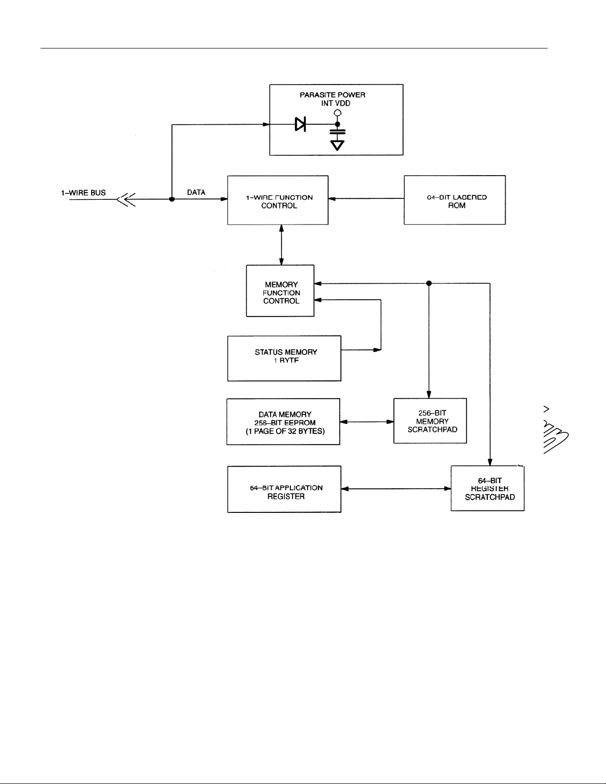
DS2430A BLOCK DIAGRAM Figure 1
DS2430A
3 of 16
Page 4
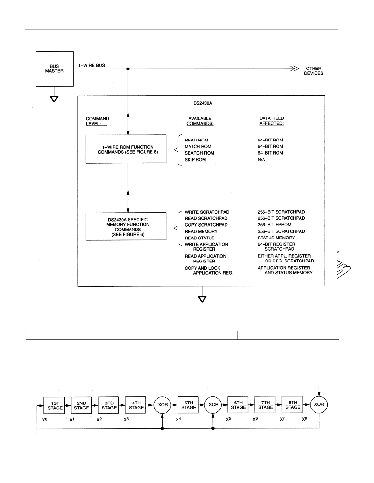
HIERARCHICAL STRUCTURE FOR 1-WIRE PROTOCOL Figure 2
DS2430A
64-BIT LASERED ROM Figure 3
8-Bit CRC Code 48-Bit Serial Number 8-Bit Family Code (14H)
MSB LSB MSB LSB MSB LSB
1-WIRE CRC GENERATOR Figure 4
Polynomial = X8 + X5 + X4 + 1
4 of 16
Page 5
DS2430A
MEMORY
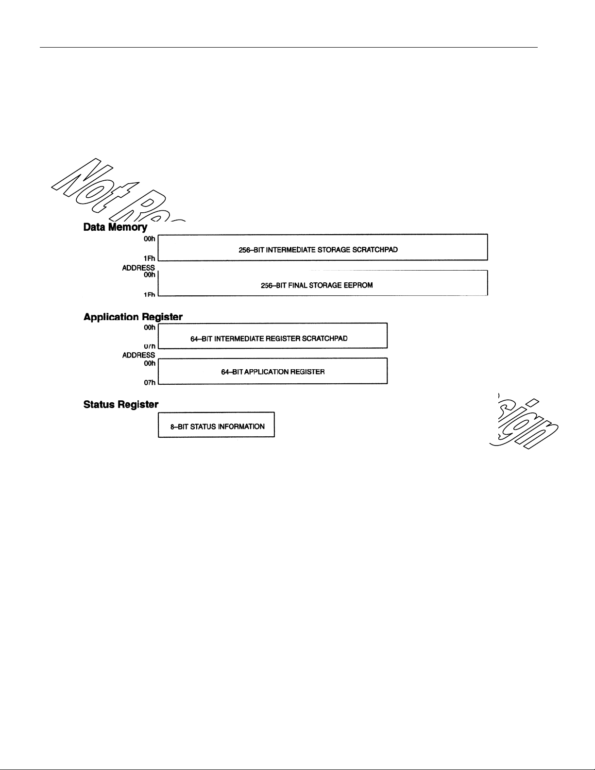
The memory of the DS2430A consists of three separate sections, called data memory, application
register, and status register (Figure 5). The data memory and the application register each have its own
intermediate storage area called scratchpad that acts as a buffer when writing to the device. The data
memory can be read and written as often as desired. The application register, however, is one-time
programmable only. Once the application register is programmed, it is automatically write protected. The
status register will indicate if the application register is already locked or if it is still available for storing
data. As long as the application register is unprogrammed, the status register will read FFh. Copying data
from the register scratchpad to the application register will clear the 2 least significant bits of the status
register, yielding an FCh the next time one reads the status register.
DS2430A MEMORY MAP Figure 5
MEMORY FUNCTION COMMANDS
The Memory Function Flow Chart (Figure 6) describes the protocols necessary for accessing the different
memory sections of the DS2430A. An example is shown later in this document.
WRITE SCRATCHPAD [0Fh]
After issuing the Write Scratchpad command, the master must first provide a 1-byte address, followed by
the data to be written to the scratchpad for the data memory. The DS2430A will automatically increment
the address after every byte it received. After having received a data byte for address 1Fh, the address
counter will wrap around to 00h for the next byte and writing continues until the master sends a Reset
Pulse.
READ SCRATCHPAD [AAh]
This command is used to verify data previously written to the scratchpad before it is copied into the final
storage EEPROM memory. After issuing the Read Scratchpad command, the master must provide the 1byte starting address from where data is to be read. The DS2430A will automatically increment the
address after every byte read by the master. After the data of address 1Fh has been read, the address
counter will wrap around to 00h for the next byte and reading continues until the master sends a Reset
Pulse.
5 of 16
Page 6

MEMORY FUNCTION FLOW CHART Figure 6
DS2430A
COPY SCRATCHPAD [55h]
After the data stored in the scratchpad has been verified the master may send the Copy Scratchpad
command followed by a validation key of A5h to transfer data from the scratchpad to the EEPROM
memory. This command will always copy the data of the entire scratchpad. Therefore, if one desires to
change only a few bytes of the EEPROM data, the scratchpad should contain a copy of the latest
EEPROM data before the Write Scratchpad and Copy Scratchpad commands are issued. After this
command is issued, the data line must be held at logic high level for at least 10ms.
READ MEMORY [F0h]
The Read Memory command is used to read a portion or all of the EEPROM data memory and to copy
the entire data memory into the scratchpad to prepare for changing a few bytes. To copy data from the
data memory to the scratchpad and to read it, the master must issue the read memory command followed
by the 1-byte starting address from where data is to be read from the scratchpad. The DS2430A will
automatically increment the address after every byte read by the master. After the data of address 1Fh has
been read, the address counter will wrap around to 00h for the next byte and reading continues until the
master sends a Reset Pulse. If one intends to copy the entire data memory to the scratchpad without
reading data, a starting address is not required; the master may send a Reset Pulse immediately following
the command code.
6 of 16
Page 7

MEMORY FUNCTION FLOW CHART Figure 6 (cont’d)
DS2430A
WRITE APPLICATION REGISTER [99h]
This command is essentially the same as the Write Scratchpad command, but it addresses the 64-bit
register scratchpad. After issuing the command code, the master must provide a 1-byte address, followed
by the data to be written. The DS2430A will automatically increment the address after every byte it
received. After having received a data byte for address 07h, the address counter will wrap around to 00h
for the next byte and writing continues until the master sends a Reset Pulse. The Write Application
Register command can be used as long as the application register has not yet been locked. If issued for a
device with the application register locked, the data written to the register scratchpad will be lost.
READ STATUS REGISTER [66h]
The status register is a means for the master to find out if the application register has been programmed
and locked. After issuing the read status register command, the master must provide the validation key
00h before receiving status information. The two least significant bits of the 8-bit status register will be 0
if the application register was programmed and locked; all other bits will always read 1. The master may
finish the read status command by sending a Reset Pulse at any time.
7 of 16
Page 8

MEMORY FUNCTION FLOW CHART Figure 6 (cont’d)
DS2430A
READ APPLICATION REGISTER [C3h]
This command is used to read the application register or the register scratchpad. As long as the
application register is not yet locked, one will receive data from the register scratchpad. After the
application register is locked the DS2430A will transmit data from the application register, making the
register scratchpad inaccessible for reading. The contents of the status register indicate where the data
received with this command came from. After issuing the Read Application Register command, the
master must provide the 1-byte starting address from where data is to be read. The DS2430A will
automatically increment the address after every byte read by the master. After the data of address 07h has
been read, the address counter will wrap around to 00h for the next byte and reading continues until the
master sends a Reset Pulse.
COPY & LOCK APPLICATION REGISTER [5Ah]
After the data stored in the register scratchpad has been verified the master may send the Copy & Lock
Application Register command followed by a validation key of A5h to transfer the contents of the entire
register scratchpad to the application register and to simultaneously write-protect it. The master may
cancel this command by sending a Reset Pulse instead of the validation key. After the validation key was
transmitted, the application register will contain the data of the register scratchpad. Further write accesses
to the application register will be denied. The Copy & Lock Application Register command can only
be executed once.
8 of 16
Page 9

DS2430A
1-WIRE BUS SYSTEM
The 1-Wire bus is a system that has a single bus master and one or more slaves. In all instances, the
DS2430A is a slave device. The bus master is typically a microcontroller. The discussion of this bus
system is broken down into three topics: hardware configuration, transaction sequence, and 1-Wire
signaling (signal type and timing). A 1-Wire protocol defines bus transactions in terms of the bus state
during specified time slots that are initiated on the falling edge of sync pulses from the bus master.
Hardware Configuration
The 1-Wire bus has only a single line by definition; it is important that each device on the bus be able to
drive it at the appropriate time. To facilitate this, each device attached to the 1-Wire bus must have open
drain connection or three-state outputs. The 1-Wire port of the DS2430A is open drain with an internal
circuit equivalent to that shown in Figure 7. A multidrop bus consists of a 1-Wire bus with multiple
slaves attached. The DS2430A communicates at regular 1-Wire speed, 16.3kbits per second, and requires
a pullup resistor as shown in Figure 7. The idle state for the 1-Wire bus is high. If for any reason a
transaction needs to be suspended, the bus MUST be left in the idle state if the transaction is to resume. If
this does not occur and the bus is left low for more than 120µs, one or more of the devices on the bus may
be reset.
HARDWARE CONFIGURATION Figure 7
RPU
RPU
Note: Depending on the 1-Wire communication speed and the bus characteristics, the optimal pullup
resistor value will be in the 1.5kΩ to 5kΩ range. To write to a single device, a 2.2kΩ resistor and V
at least 4.0V is sufficient. For writing multiple DS2430As simultaneously or operation at low V
resistor should be bypassed by a low-impedance pullup to V
while the device copies the scratchpad to
PUP
PUP
PUP
, the
of
EEPROM.
9 of 16
Page 10

ROM FUNCTIONS FLOW CHART Figure 8
DS2430A
10 of 16
Page 11

DS2430A
Transaction Sequence
The sequence for accessing the DS2430A via the 1-Wire port is as follows:
Initialization
ROM Function Command
Memory Function Command
Transaction/Data
INITIALIZATION
All transactions on the 1-Wire bus begin with an initialization sequence. The initialization sequence
consists of a Reset Pulse transmitted by the bus master followed by a Presence Pulse(s) transmitted by the
slave(s).
The Presence Pulse lets the bus master know that the DS2430A is on the bus and is ready to operate. For
more details, see the 1-Wire Signaling section.
ROM FUNCTION COMMANDS
Once the bus master has detected a presence, it can issue one of the four ROM function commands. All
ROM function commands are 8 bits long. A list of these commands follows (refer to flowchart in Figure
8):
Read ROM [33h]
This command allows the bus master to read the DS2430A’s 8-bit family code, unique 48-bit serial
number, and 8-bit CRC. This command can be used only if there is a single DS2430A on the bus. If more
than one slave is present on the bus, a data collision will occur when all slaves try to transmit at the same
time (open drain will produce a wired-AND result). The resultant family code and 48-bit serial number
will usually result in a mismatch of the CRC.
Match ROM [55h]
The Match ROM command, followed by a 64-bit ROM sequence, allows the bus master to address a
specific DS2430A on a multidrop bus. Only the DS2430A that exactly matches the 64-bit ROM sequence
will respond to the subsequent memory function command. All slaves that do not match the 64-bit ROM
sequence will wait for a Reset Pulse. This command can be used with a single or multiple devices on the
bus.
Skip ROM [CCh]
This command can save time in a single-drop bus system by allowing the bus master to access the
memory functions without providing the 64-bit ROM code. If more than one slave is present on the bus
and a read command is issued following the Skip ROM command, data collision will occur on the bus as
multiple slaves transmit simultaneously (open drain pulldowns will produce a wired-AND result).
Search ROM [F0h]
When a system is initially brought up, the bus master might not know the number of devices on the 1Wire bus or their 64-bit ROM codes. The Search ROM command allows the bus master to use a process
of elimination to identify the 64-bit ROM codes of all slave devices on the bus. The Search ROM process
is the repetition of a simple, three-step routine: read a bit, read the complement of the bit, then write the
desired value of that bit. The bus master performs this simple, three-step routine on each bit of the ROM.
11 of 16
Page 12

DS2430A
After one complete pass, the bus master knows the contents of the ROM in one device. The remaining
number of devices and their ROM codes may be identified by additional passes. See Application Note
187 for a comprehensive discussion of a search ROM, including an actual example.
1-Wire Signaling
The DS2430A requires strict protocols to insure data integrity. The protocol consists of four types of
signaling on one line: Reset Sequence with Reset Pulse and Presence Pulse, Write 0, Write 1 and Read
Data. All these signals (except Presence Pulse) are initiated by the bus master. The initialization sequence
required to begin any communication with the DS2430A is shown in Figure 9. A Reset Pulse followed by
a Presence Pulse indicates the DS2430A is ready to accept a ROM command. The bus master transmits
(TX) a Reset Pulse (t
, minimum 480µs). The bus master then releases the line and goes into receive
RSTL
mode (RX). The 1-Wire bus is pulled to a high state via the pullup resistor. After detecting the rising edge
on the data pin, the DS2430A waits (t
, 15µs to 60µs) and then transmits the Presence Pulse (t
PDH
PDL
, 60µs
to 240µs).
INITIALIZATION PROCEDURE “RESET AND PRESENCE PULSES” Figure 9
In order not to mask interrupt signaling by other devices on the 1-Wire bus, t
+ tR should always be
RSTL
less than 960µs.
Read/Write Time Slots
The definitions of write and read time slots are illustrated in Figure 10. All time slots are initiated by the
master driving the data line low. The falling edge of the data line synchronizes the DS2430A to the
master by triggering a delay circuit in the DS2430A. During write time slots, the delay circuit determines
when the DS2430A will sample the data line. For a read data time slot, if a “0” is to be transmitted, the
delay circuit determines how long the DS2430A will hold the data line low overriding the 1 generated by
the master. If the data bit is a “1”, the DS2430A will leave the read data time slot unchanged.
12 of 16
Page 13

READ/WRITE TIMING DIAGRAM Figure 10
Write-1 Time Slot
DS2430A
Write-0 Time Slot
Read-data Time Slot
13 of 16
Page 14

MEMORY FUNCTION EXAMPLE
Example: Write 2 data bytes to data memory location 0006 and 0007. Read entire data memory.
MASTER MODE DATA (LSB FIRST) COMMENTS
TX Reset Reset pulse (480µs to 960µs)
RX Presence Presence pulse
TX CCh Issue “Skip ROM” command
TX 0Fh Issue “Write Scratchpad” command
TX 06h Start address = 06h
TX <2 Data Bytes> Write 2 bytes of data to scratchpad
TX Reset Reset pulse
RX Presence Presence pulse
TX CCh Issue “Skip ROM” command
TX AAh Issue “Read Scratchpad” command
TX 06h Start address = 06h
RX <2 Data Bytes> Read scratchpad data and verify
TX Reset Reset pulse
RX Presence Presence pulse
TX CCh Issue “Skip ROM” command
TX 55h Issue “Copy Scratchpad” command
TX A5h Validation key
Data line is held high for 10ms by the bus master to
TX <Data Line High>
TX Reset Reset pulse
RX Presence Presence pulse
TX CCh Issue “Skip ROM” command
TX F0h Issue “Read Memory” command
TX 00h Start address = 00h
RX <32 Bytes> Read EEPROM data page
TX Reset Reset pulse
RX Presence Presence pulse
provide energy for copying data from the scratchpad to
EEPROM
DS2430A
14 of 16
Page 15

DS2430A
ABSOLUTE MAXIMUM RATINGS*
Voltage on DATA to Ground -0.5V to +7.0V
Operating Temperature Range -40°C to +85°C
Storage Temperature Range -55°C to +125°C
Soldering Temperature See J-STD-020A Specification
* This is a stress rating only and functional operation of the device at these or any other conditions
above those indicated in the operation sections of this specification is not implied. Exposure to
absolute maximum rating conditions for extended periods of time may affect reliability.
DC ELECTRICAL CHARACTERISTICS (-40°C to +85°C; V
= 2.8V to 6.0V)
PUP
PARAMETER SYMBOL MIN TYP MAX UNITS NOTES
Logic 1 VIH 2.2 V 1, 6
Logic 0 VIL -0.3 +0.8 V 1, 9
Output Logic Low @ 4mA VOL 0.4 V 1
Output Logic High VOH V
6.0 V 1, 2
PUP
Input Load Current (DATA pin) IL 5 μA 3
Programming Current IP 500 μA
CAPACITANCE (tA = +25°C)
PARAMETER SYMBOL MIN TYP MAX UNITS NOTES
Capacitance CD 800 pF 7
ENDURANCE (V
PARAMETER SYMBOL MIN TYP MAX UNITS NOTES
Write/Erase Cycles N
100k - 10
CYCLE
AC ELECTRICAL CHARACTERISTICS (-40°C to +85°C; V
PARAMETER SYMBOL MIN TYP MAX UNITS NOTES
Time Slot t
Write 1 Low Time t
Write 0 Low Time t
Read Low Time t
Read Data Valid t
Release Time t
Read Data Setup tSU 1 µs 5
Recovery Time t
Reset Time High t
Reset Time Low t
Presence Detect High t
Presence Detect Low t
Programming Time t
60 120 µs
SLOT
1 15 µs 13
LOW1
60 120 µs
LOW0
1 15 µs 13
LOWR
15 µs 11, 12
RDV
RELEASE
0 15 45 µs
1 µs
REC
480 µs 4
RSTH
480 960 µs 8
RSTL
15 60 µs
PDH
60 240 µs
PDL
10 ms
PROG
= 5.0V; tA = +25°C)
PUP
=2.8V to 6.0V)
PUP
15 of 16
Page 16

DS2430A
NOTES:
1) All voltages are referenced to ground.
2) V
3) Input load is to ground.
4) An additional reset or communication sequence cannot begin until the reset high time has expired.
5) Read data setup time refers to the time the host must pull the 1-Wire bus low to read a bit. Data is
6) V
7) Capacitance on the data pin could be 800pF when power is first applied. If a 5kΩ resistor is used to
8) The Reset Low Time (t
9) Under certain low voltage conditions V
10) The Copy Scratchpad takes 10ms maximum, during which the voltage on the 1-Wire bus must not fall
11) Depending on the 1-Wire communication speed and the bus load characteristics, the optimal pullup
12) The optimal sampling point for the master is as close as possible to the end time of the 15μs t
13) The duration of the low pulse sent by the master should be a minimum of 1μs with a maximum value
= external pullup voltage.
PUP
guaranteed to be valid within 1μs of this falling edge.
is a function of the external pullup resistor and V
IH
pull up the data line to V
, 5μs after power has been applied the parasite capacitance will not affect
PUP
PUP
.
normal communications.
) should be restricted to a maximum of 960μs, to allow interrupt signaling;
RSTL
otherwise it could mask or conceal interrupt pulses.
may have to be reduced to as much as 0.5V to always
ILMAX
guarantee a Presence Pulse.
below 2.8V.
resistor value will be in the 1.5kΩ to 5kΩ range.
RDV
period without exceeding t
. For the case of a Read-One Time slot, this maximizes the amount of
RDV
time for the pullup resistor to recover to a high level. For a Read-Zero Time slot, it ensures that a read
will occur before the fastest 1-Wire device(s) releases the line.
as short as possible to allow time for the pullup resistor to recover the line to a high level before the 1Wire device samples in the case of a Write-One Time or before the master samples in the case of a
Read-One Time.
16 of 16
 Loading...