

Page 1
19-5316; 7/10
2
y
www.maxim-ic.com
GENERAL DESCRIPTION
The DS2413 is a dual-channel programmable I/O
®
1-Wire
chip. The PIO outputs are configured as
open-drain and provide up to 20mA continuous sink
capability and off-state operating voltage up to 28V.
Control and sensing of the PIO pins is performed with
a dedicated device-level command protocol. To
provide a high level of fault tolerance in the end
application, the 1-Wire IO and PIO pins are all
capable of withstanding continuous application of
voltages up to 28V max. Communication and
operation of the DS2413 is performed with the single
contact Maxim/Dallas 1-Wire serial interface.
APPLICATIONS
LED Control
Accessory Identification and Control
General Purpose Input/Output
Key-Pick Systems
Industrial Controllers
System Monitoring
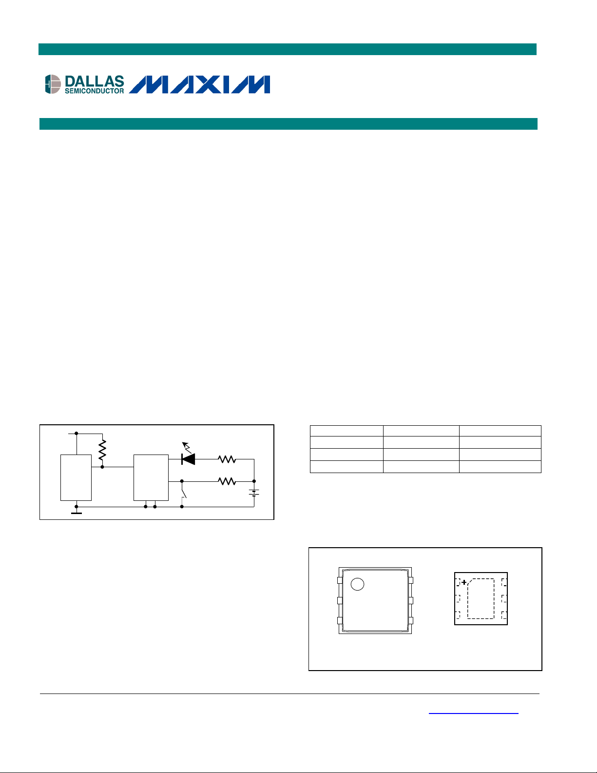
TYPICAL OPERATING CIRCUIT
V
CC
R
PUP
PX.Y
µC
mands, Registers, and Modes are capitalized for
Com
clarity.
1-Wire is a registered trademark of Maxim Integrated Products, Inc.
DS2413
IO
GND
PIOA
PIOB
LED
Switch
Local
Power
R1
R2
DS2413
1-Wire Dual Channel
Addressable Switch
FEATURES
Open-Drain Programmable I/O Pins
PIO Pins Support 20mA max Continuous Current
Sink
Supports 28V (max) PIO Pin Operating Voltage
On-Resistance of PIO Pulldown Transistor 20
max; OFF Resistance 1M min
Parasitic Power Supply Through 1-Wire
Communicates to Host with a Single Digital
Signal at 14.9kb or 100kbps Using 1-Wire
Protocol
Unique 64-bit ROM Serial Number Factory
Lasered Into Each Device
Switchpoint Hysteresis and Filtering to Optimize
Performance in the Presence of Noise
1-Wire IO Pin Supports 28V Absolute Maximum
DC Level for Fault Conditions
Operates Over a Wide 1-Wire Voltage Range of
2.8V to 5.25V from 0°C to +70°C
High ESD Immunity of 1-Wire IO Pin: 8kV HBM
Typical
TSOC and TDFN Packages Available
ORDERING INFORMATION
PART TEMP RANGE PIN-PACKAGE
DS2413P+ 0°C to +70°C TSOC
DS2413P+T&R 0°C to +70°C TSOC
DS2413Q+T&R 0°C to +70°C TDFN
+ Denotes a lead(Pb)-free package/RoHS-compliant
package.
T&R = Tape and reel.
PIN CONFIGURATION
TSOC TDFN
ywwrr
6
5
4
1
2
3
Exposed Paddle
413
mrrF
6
5
4
1
2
DS
3
Top View with Marking. TDFN Contacts
2413
Not Visible in this View.
Note: Some revisions of this device may incorporate deviations from published specifications known as errata. Multiple revisions of any device
may be simultaneously available through various sales channels. For information about device errata, click here: www.maxim-ic.com/errata
1 of 18
.
Page 2
DS2413: 1-Wire Dual Channel Addressable Switch
ABSOLUTE MAXIMUM RATINGS
Voltage on Any Pin to GND -0.5V, +30V
Maximum Current into IO Pin
Maximum Current into PIO Pin
Maximum Current Through GND Pins (Both Pins Tied Together)
Operating Temperature Range 0°C to +70°C
Junction Temperature +150°C
Storage Temperature Range -55°C to +125°C
Lead Temperature (soldering, 10s)
Soldering Temperature (reflow)
Stresses beyond those listed under “Absolute Maximum Ratings” may cause permanent damage to the device. These are stress ratings only,
and functional operation of the device at these or any other conditions beyond those indicated in the operational sections of the specifications is
not implied. Exposure to the absolute maximum rating conditions for extended periods may affect device reliability.
ELECTRICAL CHARACTERISTICS T
= 0°C to +70°C
A
PARAMETER SYMBOL CONDITIONS MIN TYP MAX UNITS
IO PIN GENERAL DATA
1-Wire Pullup Voltage
(Note 1)
1-Wire Pullup Resistance
V
R
Input Load Current I
PUP
PUP
L
Standard speed 2.8 5.25
Overdrive speed 2.9 5.25
DC only; no 1-Wire communication 28
(Notes 1, 2)
V
5.25V
PUP
V
3.30V
PUP
1.5 2.2
3.5 70
3.5 15
V(IO) = 28V (Note 3) 400 950
Input Capacitance CIO At 25°C (Notes 4, 5) 800 pF
Input Low Voltage V
High-to-Low Switching
Threshold
Low-to-High Switching
Threshold
Switching Hysteresis V
Output Low Voltage V
Recovery Time
(Notes 1, 12)
(Notes 5, 13)
Time slot Duration
(Note 1, 5)
t
t
t
IL
V
TL
V
TH
HY
OL
REC
REH
SLOT
(Notes 1, 6) 0.4 V
(Notes 5, 7, 8) 0.4 3.2 V
(Notes 5, 7, 9) 0.7 3.6 V
(Notes 5, 10) 0.2 V
At 4mA Current Load (Note 11)
Standard speed, R
Overdrive speed, R
PUP
PUP
= 2.2k
= 2.2k
Overdrive speed, directly prior to reset
pulse; R
PUP
= 2.2k
0.4 V
5
2
5
Standard speed 0.5 5.0 Rising-Edge Hold-off Time
Overdrive speed Not applicable (0)
Standard speed, V
PUP
4.5V
65
Standard speed (Note 14) 67
Overdrive speed, V
(Note 14)
PUP
4.5V
9
Overdrive speed (Note 14) 10
IO PIN, 1-Wire RESET, PRESENCE DETECT CYCLE
480 960
48 80
63 80
15
2
66
7.0
8.2
0 0.7
Reset Low Time (Note 1) t
Presence Detect High
Time (Notes 14, 15)
Presence Detect Fall Time
(Notes 5, 16)
RSTL
t
PDH
t
FPD
Standard speed, V
Standard speed (Note 14) 600 960
Overdrive speed, V
PUP
PUP
4.5V
4.5V
Overdrive speed (Note 14)
Standard speed, V
Standard speed 15 68
Overdrive speed, V
PUP
PUP
4.5V
4.5V
Overdrive speed 2
Standard speed, V
Standard speed 0.24 1.6
Overdrive speed, V
> 4.5V 0.24 1.4
PUP
4.5V
PUP
Overdrive speed 0 0.9
Presence Detect Low
Time (Note 15)
t
PDL
Standard speed, V
Standard speed (Note 14) 60 260
Overdrive speed, V
(Note 14)
Overdrive speed (Note 14) 8
> 4.5V 60 240
PUP
4.5V
PUP
8
25
32
25mA
30mA
60mA
+300°C
+260°C
V
k
µA
µs
µs
µs
µs
µs
µs
µs
2 of 18
Page 3
DS2413: 1-Wire Dual Channel Addressable Switch
PARAMETER SYMBOL CONDITIONS MIN TYP MAX UNITS
Presence Detect Sample
Time (Notes 1, 20)
t
MSP
Standard speed, V
Standard speed 69.6 75
Overdrive speed, V
> 4.5V 67.4 75
PUP
PUP
4.5V
7.7 10
µs
Overdrive speed 9.1 10
IO PIN, 1-Wire WRITE
Write-0 Low Time
(Notes 1, 17)
t
W0L
Standard speed, V
Standard speed (Note 14) 62 120
Overdrive speed, V
(Note 14)
> 4.5V 60 120
PUP
4.5V
PUP
7 16
µs
Overdrive speed (Note 14) 8 16
(Notes 1, 17)
t
W1L
Standard speed 5 15 Write-1 Low Time
Overdrive speed 1 2
µs
IO PIN, 1-Wire READ
Read Low Time
(Notes 1, 18)
Read Sample Time
(Notes 1, 18)
t
t
MSR
RL
Standard speed 5
Overdrive speed 1
Standard speed
Overdrive speed
t
+
RL
t
+
RL
15
2
15 -
2 -
µs
µs
PIO Pins
Leakage Current ILP Pin at 28V (Note 19) 8.5 24 µA
Input Capacitance CP (Note 5) 100 pF
Output low voltage V
Input Low Voltage V
Input High Voltage
(Note 21)
V
OLP
ILP
IHP
20mA load current 0.4 V
(Note 1) 0.8 V
–
V
(Note 1)
PUP
0.3V
28 V
Note 1: System requirement.
Note 2: Full R
Maximum allowable pullup resistance is a function of the number of 1-Wire devices in the system and 1-Wire recovery times. The
specified value here applies to systems with only one device and with the minimum 1-Wire recovery times. For more heavily
loaded systems, an active pullup such as that found in the DS2482-x00 or DS2480B may be required. The DS2482-x00 may not
always detect the DS2413 presence pulse. For proper operation it may be necessary to disregard (force to 1) the PPD bit in the
DS2482-x00 status register.
Note 3: The I-V characteristic is linear for voltages greater than 10V.
Note 4:
Capacitance on the data pin could be 800pF when V
after V
Note 5: Guaranteed by design and simulation. Not production tested.
Note 6: The voltage on IO needs to be less than or equal to V
Note 7: V
V
Note 8: Voltage below which, during a falling edge on IO, a logic 0 is detected.
Note 9: Voltage above which, during a rising edge on IO, a logic 1 is detected.
Note 10: After V
Note 11: The I-V characteristic is linear for voltages less than 1V.
Note 12: Applies to a single DS2413 attached to a 1-Wire line.
Note 13: The earliest recognition of a negative edge is possible at t
Note 14: Highlighted numbers are NOT in compliance with legacy 1-Wire product standards. See comparison table below.
Note 15: t
pulse. t
Note 16: Interval during the negative edge on IO at the beginning of a Presence Detect pulse between the time at which the voltage is
80% of V
Note 17:
in Figure 12 represents the time required for the pullup circuitry to pull the voltage on IO up from V
duration for the master to pull the line low is t
Note 18:
in Figure 12 represents the time required for the pullup circuitry to pull the voltage on IO up from V
of the bus master. The actual maximum duration for the master to pull the line low is t
Note 19: The I-V characteristic is linear for voltages greater than 7V.
Note 20: t
t
Note 21: Production tested for V
range guaranteed by design and simulation. not production tested. Production testing performed at a fixed R
PUP
is first applied. If a 2.2k resistor is used to pull up the data line, 2.5µs
has been applied the parasite capacitance will not affect normal communications.
PUP
and VTH are functions of the internal supply voltage, which is a function of V
TL
maximum specifications are valid at V
TL
is crossed during a rising edge on IO, the voltage on IO has to drop by at least VHY to be detected as logic '0'.
TH
is deemed to have ended when the voltage on IO drops below 80% of V
PDH
MSP
PDH
is deemed to have begun when the voltage on IO drops below 20% of V
PDL
and the time at which the voltage is 20% of V
PUP
is a system required sample point and not directly production tested. Production testing is performed on related parameters
and t
. Parameter t
PDL
is guaranteed by design and simulation, not production tested.
FPD
. V
IHP(min)
IHP(max)
PUPmax
is guaranteed by design and simulation, not production tested.
PUP
whenever the master drives the line low.
ILMAX
(5.25V). In any case, VTL < VTH < V
after VTH has been previously reached.
REH
.
PUP
W1Lmax
+ tF - and t
+ tF - respectively.
W0Lmax
and the 1-Wire Recovery Times. The VTH and
PUP
.
PUP
on the leading edge of the presence-detect low
PUP
on the leading edge of the pulse.
PUP
to VTH. The actual maximum
IL
to the input high threshold
RLmax
+ tF.
IL
PUP
value.
3 of 18
Page 4
DS2413: 1-Wire Dual Channel Addressable Switch
LEGACY VALUES DS2413 VALUES
PARAMETER STANDARD SPEED OVERDRIVE SPEED STANDARD SPEED OVERDRIVE SPEED
MIN MAX MIN MAX MIN MAX MIN MAX
t
SLOT
t
RSTL
t
PDH
t
PDL
t
W0L
(incl. t
REC)
61µs (undef.) 7µs (undef.) 67µs (undef.) 10µs (undef.)
480µs (undef.) 48µs 80µs 600µs 960µs 63µs 80µs
15µs 60µs 2µs 6µs 15µs 68µs 2µs 8.2µs
60µs 240µs 8µs 24µs 60µs 260µs 8µs 32µs
60µs 120µs 6µs 16µs 62µs 120µs 8µs 16µs
PIN DESCRIPTION
NAME TSOC PIN # TDFN PIN # FUNCTION
IO 2 2 1-Wire bus interface. Open-drain, requires external pullup resistor.
PIOA 6 4 Programmable I/O pin, open-drain with weak pulldown, power-on
default is off (PIOA = 1).
PIOB 4 6 Programmable I/O pin, open-drain with weak pulldown, power-on
default is off (PIOB = 1).
GND1 1 3 Ground reference 1
GND2 5 5 Ground reference 2; both GND pins must be connected in the
application.
NC 3 1 Not connected
Exposed Paddle (TDFN only). Solder evenly to the board’s ground
GND — EP
plane for proper operation. See Application Note 3273 for additional
information.
DESCRIPTION
The DS2413 combines two PIO pins and a fully featured 1-Wire interface in a single chip. PIO outputs are opendrain, operate at up to 28V and provide an on resistance of 20 max. A robust communication protocol ensures
that PIO output changes occur error-free. Each DS2413 has a Registration Number that is 64 bits long. The
Registration Number guarantees unique identification and is used to address the device in a multidrop 1-Wire
network environment, where multiple devices reside on a common 1-Wire bus and operate independently of each
other. Device power is supplied parasitically from the 1-Wire bus. The DS2413’s applications of include accessory
identification and control, system monitoring, and general-purpose input/output.
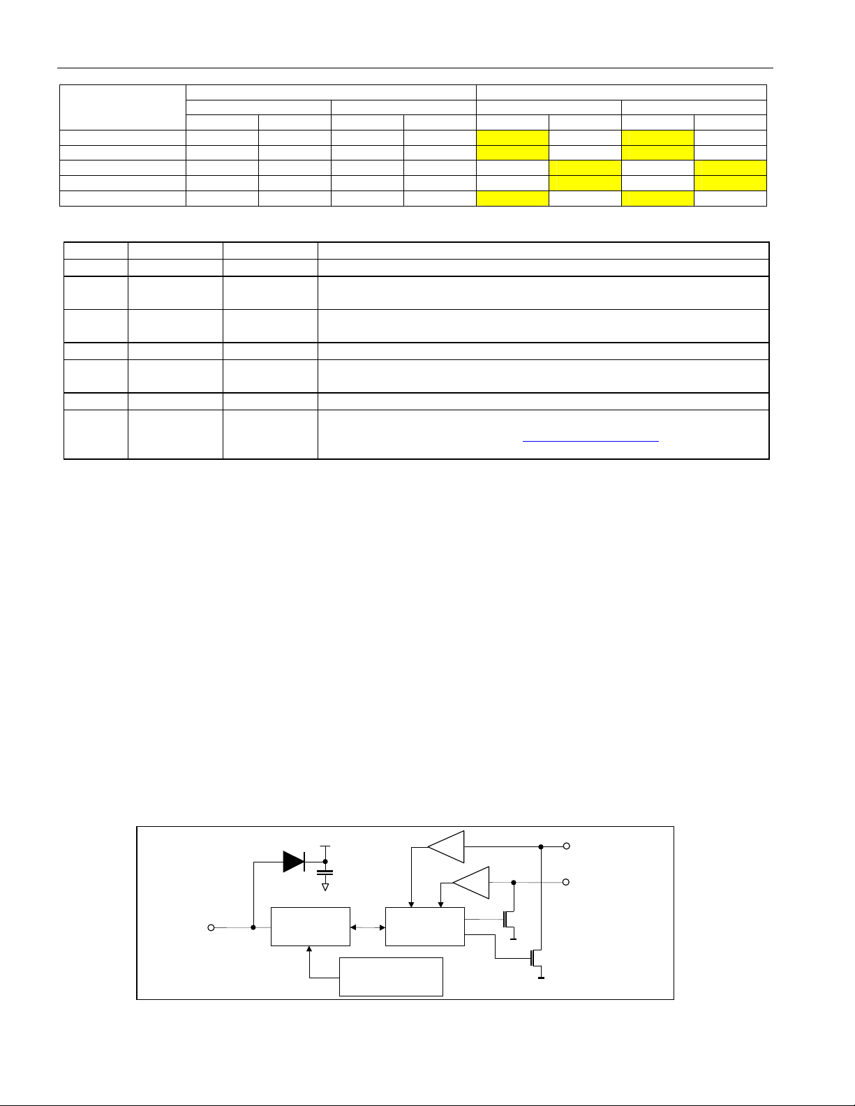
OVERVIEW
The block diagram in Figure 1 shows the relationships between the major sections of the DS2413. The DS2413
has two main components: 64-bit Registration Number, and PIO Control. The hierarchical structure of the 1-Wire
protocol is shown in Figure 2. The bus master must first provide one of the seven ROM Function Commands, 1)
Read ROM, 2) Match ROM, 3) Search ROM, 4) Skip ROM, 5) Resume, 6) Overdrive-Skip ROM or 7) OverdriveMatch ROM. Upon completion of an Overdrive ROM command byte executed at standard speed, the device enters
Overdrive mode where all subsequent communication occurs at a higher speed. The protocol required for these
ROM function commands is described in Figure 10. After a ROM function command is successfully executed, the
PIO functions become accessible and the master may provide one of the two PIO Function commands. The
protocol for these commands is described in Figure 6. All data is read and written least significant bit first.
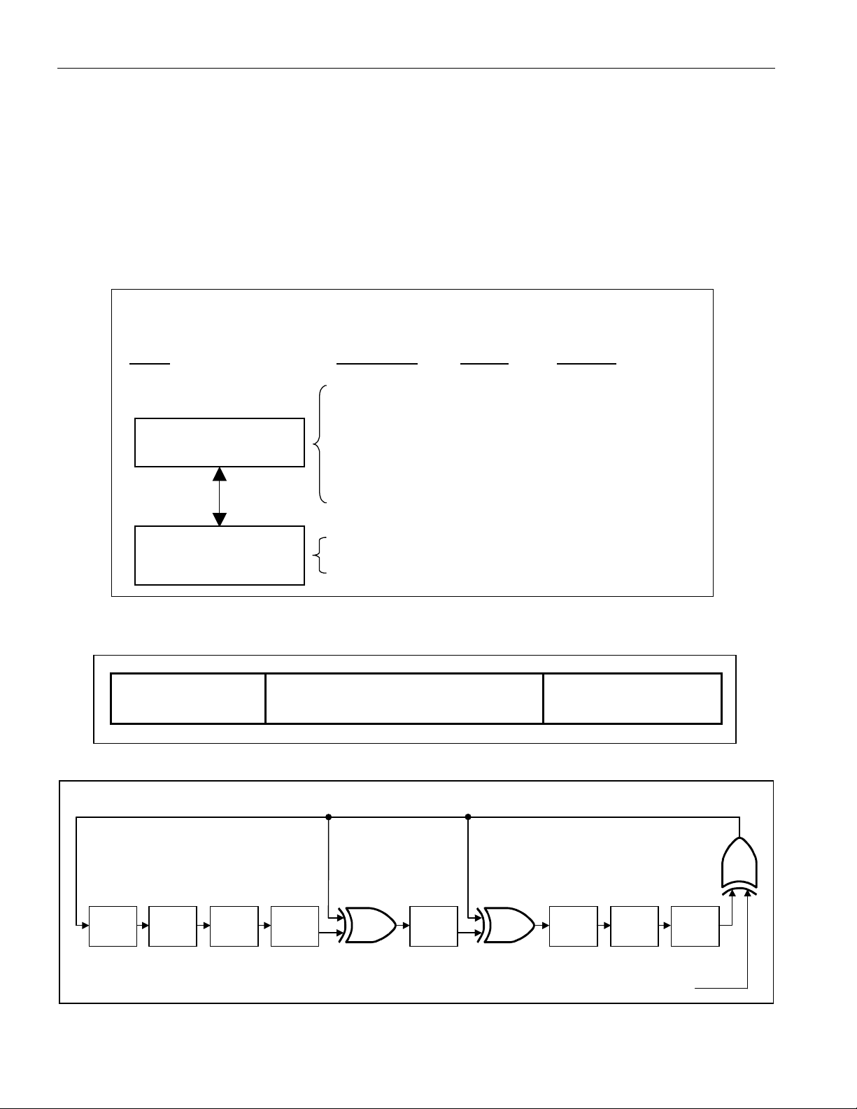
Figure 1. Block Diagram
IO
Internal V
1-Wire
Interface
DD
PIO
Control
64-Bit Registration
Number
4 of 18
PIOB
PIOA
Page 5
DS2413: 1-Wire Dual Channel Addressable Switch
A
64-BIT LASERED ROM
Each DS2413 has a unique ROM Registration Number that is 64 bits long, as shown in Figure 3. The first eight bits
are a 1-Wire family code. The next 48 bits are a unique serial number. The last eight bits are a CRC (Cyclic
Redundancy Check) of the first 56 bits. The 1-Wire CRC is generated using a polynomial generator consisting of a
shift register and XOR gates as shown in Figure 4. The polynomial is X
8
+ X5 + X4 + 1. Additional information about
the Dallas 1-Wire CRC is available in Application Note 27. The shift register bits are initialized to zero. Then
starting with the LSB of the family code, one bit at a time is shifted in. After the 8th bit of the family code has been
entered, then the serial number is entered. After the 48th bit of the serial number has been entered, the shift
register contains the CRC value. Shifting in the eight bits of CRC should return the shift register to all zeros.
Figure 2. Hierarchical Structure for 1-Wire Protocol
DS2413
Command
Level:
1-Wire ROM Function
Commands (see Figure 10)
DS2413-specific
PIO Function Commands
(see Figure 6)
Figure 3. 64-Bit LASERED ROM
MSB LSB
8-Bit CRC Code 48-Bit Serial Number
MSB LSB MSB LSB MSB LSB
Figure 4. 1-Wire CRC Generator
Available
Commands:
Read ROM
Match ROM
Search ROM
Skip ROM
Resume
Overdrive Skip
Overdrive Match
PIO Access Read
PIO Access Write
Command
Codes:
33h
55h
F0h
CCh
3Ch
69h
F5h
5Ah
5h
Data Field
Affected:
64-bit Reg. #, RC-Flag
64-bit Reg. #, RC-Flag
64-bit Reg. #, RC-Flag
RC-Flag
RC-Flag
RC-Flag, OD-Flag
64-bit Reg. #, RC-Flag,
PIO Pins
PIO Pins
8-Bit Family Code (3Ah)
OD-Flag
Polynomial = X8 + X5 + X4 + 1
0
X
st
1
STAGE
STAGE
1
X
nd
2
2
X
rd
3
STAGE
STAGE
3
X
th
4
STAGE
4
X
th
5
STAGE
5
X
th
6
STAGE
6
X
INPUT DATA
th
7
STAGE
7
X
th
8
8
X
5 of 18
Page 6
DS2413: 1-Wire Dual Channel Addressable Switch
p
PIO STUCTURE
Each PIO consists of an open-drain pulldown transistor with 28V capability. The transistor is controlled by the PIO
Output Latch, as shown in Figure 5. The PIO Control unit connects the PIOs to the 1-Wire interface.
Figure 5. PIO Simplified Logic Diagram
PIO Pin
State
PIO Output
Latch State.
PIO Pin
PIO Data
PIO Clock
CLOCK
PIO Out-
Q
ut Latch
QD
PIO FUNCTION COMMANDS
The PIO Function Flow Chart (Figure 6) describes the protocols necessary to access the PIO pins of the DS2413.
Examples on how to use these functions are included at the end of this document. The communication between
master and DS2413 takes place either at standard speed (default, OD = 0) or at Overdrive Speed (OD = 1). If not
explicitly set into the Overdrive Mode, the DS2413 powers up in standard speed.
PIO ACCESS READ [F5h]
This command reads the PIO logical status and reports it together with the state of the PIO Output Latch in an
endless loop. A PIO Access Read can be terminated at any time with a 1-Wire Reset.
PIO Status Bit Assignment
b7 b6 b5 b4 b3 b2 b1 b0
Complement of b3 to b0
The state of both PIO channels is sampled at the same time. The first sampling occurs during the last (most
significant) bit of the command code F5h. The PIO status is then reported to the bus master. While the master
receives the last (most significant) bit of the PIO status byte, the next sampling occurs and so on until the master
generates a 1-Wire Reset. The sampling occurs with a delay of t
previous byte, as shown in Figure 7. The value of "x" is approximately 0.2µs.
PIOB Output
Latch State
Figure 7. PIO Access Read Timing Diagram
MS 2 bits of
previous byte
PIOB Pin
State
V
TH
PIOA Output
Latch State
+x from the rising edge of the MS bit of the
REH
LS 2 bits of PIO
Status byte
PIOA Pin
State
IO
t
+x
REH
Sampling Point
Notes:
1
2 The sample point timing also applies to the PIO Access Write command, with the "previous byte" being the
The "previous byte" could be the command code or the data byte resulting from the previous PIO sample.
write confirmation byte (AAh).
6 of 18
Page 7

Figure 6. PIO Function Flow Chart
y
)1)
Bus Master TX Memory
Function Command
DS2413: 1-Wire Dual Channel Addressable Switch
From ROM Functions
Flow Chart (Figure 10)
Note 1)
See the command
description for the
exact timing of the
PIO pin sampling
and updating.
DS2413 Samples
PIO Pin Status
F5h
PIO Access
Read?
Y
N
1)
5Ah
PIO Access
Write?
Y
Bus Master TX new
PIO Output Data Byte
Bus Master TX
inverted new PIO
Output Data B
Transmission
OK?
DS2413 Updates
PIO Output Latch
Bus Master RX
Confirmation AAh
te
Y
N
N
Bus Master
RX “1”s
N
Master
TX Reset?
Bus Master RX
PIO Pin Status
Master
TX Reset?
Y
Y
N
To ROM Functions
Flow Chart (Figure 10)
N
7 of 18
DS2413 Samples
PIO Pin Status
Bus Master RX
PIO Pin Status
Master
TX Reset?
Y
1
Y
Page 8

DS2413: 1-Wire Dual Channel Addressable Switch
PIO ACCESS WRITE [5Ah]
The PIO Access Write command writes to the PIO output latches, which control the pulldown transistors of the PIO
channels. In an endless loop this command first writes new data to the PIO and then reads back the PIO status.
This implicit read-after-write can be used by the master for status verification. A PIO Access Write can be
terminated at any time with a 1-Wire Reset.
PIO Output Data Bit Assignment
b7 b6 b5 b4 b3 b2 b1 b0
X X X X X X PIOB PIOA
After the command code the master transmits a PIO Output Data byte that determines the new state of the PIO
output transistors. The first (least significant) bit is associated to PIOA; the next bit affects PIOB. The other 6 bits of
the new state byte do not have corresponding PIO pins. These bits should always be transmitted as "1"s. To switch
the output transistor on, the corresponding bit value is 0. To switch the output transistor off (non-conducting) the bit
must be 1. This way the bit transmitted as the new PIO output state arrives in its true form at the PIO pin. To
protect the transmission against data errors, the master must repeat the PIO Output Data byte in its inverted form.
Only if the transmission was error-free will the PIO status change. The actual PIO transition to the new state occurs
with a delay of t
of "x" is approximately 0.2µs. To inform the master about the successful communication of the PIO byte, the
DS2413 transmits a confirmation byte with the data pattern AAh. While the MS bit of the confirmation byte is
transmitted, the DS2413 samples the state of the PIO pins, as shown in Figure 7, and sends it to the master. The
master can either continue writing more data to the PIO or issue a 1-Wire Reset to end the command.
Figure 8. PIO Access Write Timing Diagram
+x from the rising edge of the MS bit of the inverted PIO byte, as shown in Figure 8. The value
REH
MS 2 bits of inverted
PIO Output Data byte
IO
PIO
t
REH
V
TH
+x
LS 2 bits of confir-
mation byte (AAh)
1-Wire BUS SYSTEM
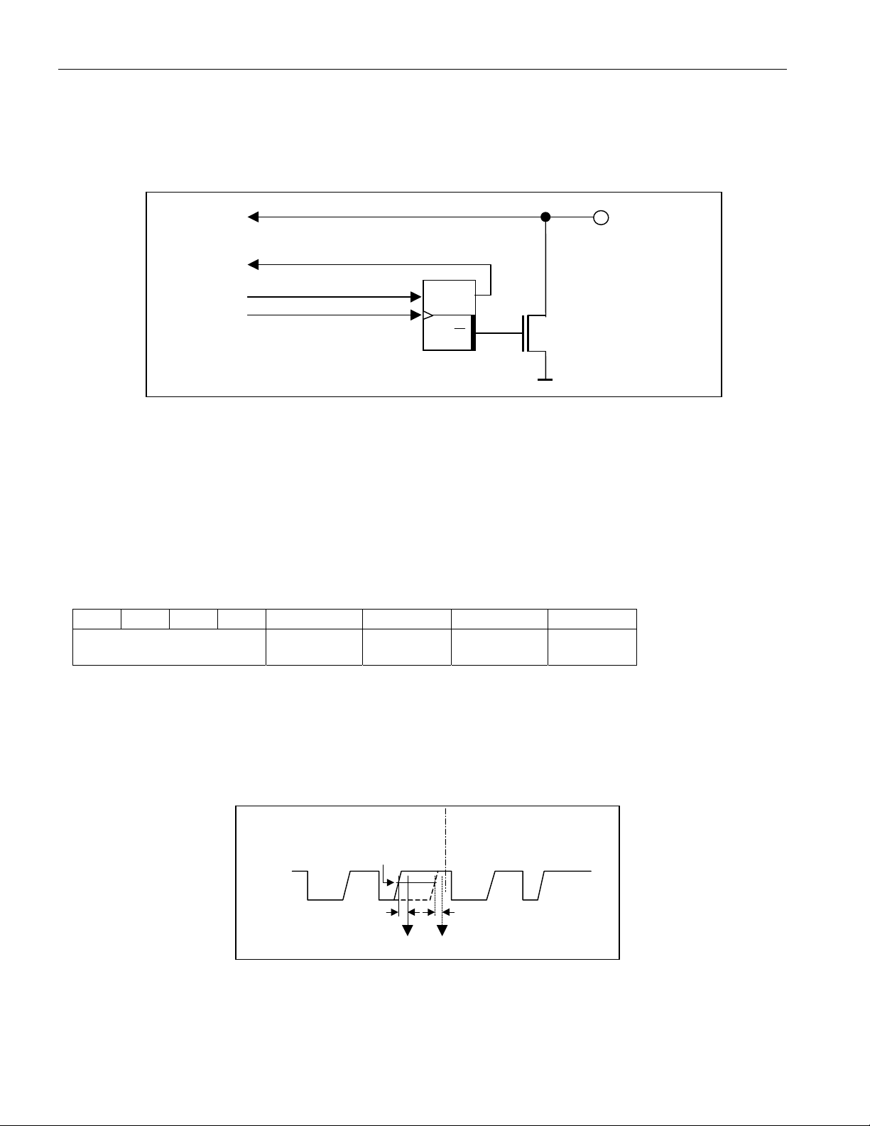
The 1-Wire bus is a system that has a single bus master and one or more slaves. In all instances the DS2413 is a
slave device. The bus master is typically a microcontroller. The discussion of this bus system is broken down into
three topics: hardware configuration, transaction sequence, and 1-Wire signaling (signal types and timing). The
1-Wire protocol defines bus transactions in terms of the bus state during specific time slots, which are initiated on
the falling edge of sync pulses from the bus master.
HARDWARE CONFIGURATION
The 1-Wire bus has only a single line by definition; it is important that each device on the bus be able to drive it at
the appropriate time. To facilitate this, each device attached to the 1-Wire bus must have open-drain or tri-state
outputs. The 1-Wire port of the DS2413 is open drain with an internal circuit equivalent to that shown in Figure 9.
A multidrop bus consists of a 1-Wire bus with multiple slaves attached. The DS2413 supports both a Standard and
Overdrive communication speed of 14.9kbps (max) and 100kbps (max), respectively. Note that legacy 1-Wire
products support a standard communication speed of 16.3kbps and Overdrive of 142kbps. The value of the pullup
resistor primarily depends on the network size and load conditions. The DS2413 requires a pullup resistor of 2.2k
(max) at any speed.
8 of 18
Page 9

DS2413: 1-Wire Dual Channel Addressable Switch
The idle state
left in the idle state if the transaction is to resume. If this does not occur and the bus is left low for more than 16µs
(Overdrive speed) or more than 120µs (standard speed), one or more devices on the bus may be reset.
for the 1-Wire bus is high. If for any reason a transaction needs to be suspended, the bus MUST be
Figure 9. Hardware Configuration
V
BUS MASTER DS2413 1-Wire PORT
PUP
R
PUP
RX
TX
Open Drain
Port Pin
RX = RECEIVE
TX = TRANSMIT
I
L
100
MOSFET
RXDATA
TX
TRANSACTION SEQUENCE
The protocol for accessing the DS2413 through the 1-Wire port is as follows:
Initialization
ROM Function Command
PIO Function Command
Data
INITIALIZATION
All transactions on the 1-Wire bus begin with an initialization sequence. The initialization sequence consists of a
reset pulse transmitted by the bus master followed by presence pulse(s) transmitted by the slave(s). The presence
pulse lets the bus master know that the DS2413 is on the bus and is ready to operate. For more details, see the 1-
Wire Signaling section.
1-Wire ROM FUNCTION COMMANDS
Once the bus master has detected a presence, it can issue one of the seven ROM function commands that the
DS2413 supports. All ROM function commands are 8 bits long. A list of these commands follows (refer to the flow
chart in Figure 10).
READ ROM [33h]
This command allows the bus master to read the DS2413’s 8-bit family code, unique 48-bit serial number, and 8-bit
CRC. This command can only be used if there is a single slave on the bus. If more than one slave is present on the
bus, a data collision occurs when all slaves try to transmit at the same time (open drain produces a wired-AND
result). The resultant family code and 48-bit serial number result in a mismatch of the CRC.
MATCH ROM [55h]
The Match ROM command, followed by a 64-bit ROM sequence, allows the bus master to address a specific
DS2413 on a multidrop bus. Only the DS2413 that exactly matches the 64-bit ROM sequence, including the
external address, responds to the following PIO Function command. All other slaves wait for a reset pulse. This
command can be used with a single or multiple devices on the bus.
9 of 18
Page 10

DS2413: 1-Wire Dual Channel Addressable Switch
SEARCH ROM [F0h]
When a system is initially brought up, the bus master might not know the number of devices on the 1-Wire bus or
their device ID numbers. By taking advantage of the wired-AND property of the bus, the master can use a process
of elimination to identify the device ID numbers of all slave devices. For each bit of the device ID number, starting
with the least significant bit, the bus master issues a triplet of time slots. On the first slot, each slave device
participating in the search outputs the true value of its device ID number bit. On the second slot, each slave device
participating in the search outputs the complemented value of its device ID number bit. On the third slot, the master
writes the true value of the bit to be selected. All slave devices that do not match the bit written by the master stop
participating in the search. If both of the read bits are zero, the master knows that slave devices exist with both
states of the bit. By choosing which state to write, the bus master branches in the ROM code tree. After one
complete pass, the bus master knows the device ID number of a single device. Additional passes identify the
device ID numbers of the remaining devices. Refer to Application Note 187: 1-Wire Search Algorithm for a detailed
discussion, including an example. Since with the DS2413 the ROM CRC is not valid if one or more address inputs
are tied to GND, it is recommended to do a double search when building a list of devices on the 1-Wire line.
SKIP ROM [CCh]
This command can save time in a single-drop bus system by allowing the bus master to access the PIO functions
without providing the 64-bit ROM code. If more than one slave is present on the bus and, for example, a read
command is issued following the Skip ROM command, data collision occurs on the bus as multiple slaves transmit
simultaneously (open-drain pulldowns produce a wired-AND result).
RESUME [A5h]
To maximize the data throughput in a multidrop environment, the Resume function is available. This function
checks the status of the RC bit and, if it is set, directly transfers control to the PIO functions, similar to a Skip ROM
command. The only way to set the RC bit is through successfully executing the Match ROM, Search ROM, or
Overdrive Match ROM command. Once the RC bit is set, the device can repeatedly be accessed through the
Resume Command function. Accessing another device on the bus clears the RC bit, preventing two or more
devices from simultaneously responding to the Resume Command function.
OVERDRIVE SKIP ROM [3Ch]
On a single-drop bus this command can save time by allowing the bus master to access the PIO functions without
providing the 64-bit ROM code. Unlike the normal Skip ROM command, the Overdrive Skip ROM sets the DS2413
in the Overdrive mode (OD = 1). All communication following this command has to occur at Overdrive speed until a
reset pulse of minimum 480µs duration resets all devices on the bus to standard speed (OD = 0).
When issued on a multidrop bus, this command sets all Overdrive-supporting devices into Overdrive mode. To
subsequently address a specific Overdrive-supporting device, a reset pulse at Overdrive speed has to be issued
followed by a Match ROM or Search ROM command sequence. This speeds up the time for the search process. If
more than one slave supporting Overdrive is present on the bus and the Overdrive Skip ROM command is followed
by a Read command, data collision occurs on the bus as multiple slaves transmit simultaneously (open-drain
pulldowns produce a wired-AND result).
OVERDRIVE MATCH ROM [69h]
The Overdrive Match ROM command followed by a 64-bit ROM sequence transmitted at Overdrive Speed allows
the bus master to address a specific DS2413 on a multidrop bus and to simultaneously set it in Overdrive mode.
Only the DS2413 that exactly matches the 64-bit ROM sequence responds to the subsequent PIO Function
command. Slaves already in Overdrive mode from a previous Overdrive Skip or successful Overdrive Match
command remain in Overdrive mode. All overdrive-capable slaves return to standard speed at the next Reset Pulse
of minimum 480µs duration. The Overdrive Match ROM command can be used with a single or multiple devices on
the bus.
10 of 18
Page 11

Figure 10-1. ROM Functions Flow Chart
d
t
From PIO Functions
Flow Chart (Figure 6)
Bus Master TX
Reset Pulse
Reset Pulse ?
Y
OD
DS2413: 1-Wire Dual Channel Addressable Switch
From Figure 10, 2
N
OD = 0
n
Par
Bus Master TX ROM
Function Command
33h
Read ROM
Command ?
RC = 0
DS2413 TX
Family Code
(1 Byte)
DS2413 TX
Serial Number
(6 Bytes)
N
Presence Pulse
55h
Match ROM
Command ?
RC = 0
Master TX Bit 0
Bit 0
Match ?
Y
Master TX Bit 1
Bit 1
Match ?
Y
DS2413 TX
N
N
N
N
N
F0h
Search ROM
Command ?
YY Y Y
RC = 0
DS2413 TX Bit 0
DS2413 TX Bit 0
Master TX Bit 0
Bit 0
Match ?
Y
DS2413 TX Bit 1
DS2413 TX Bit 1
Master TX Bit 1
Bit 1
Match ?
Y
To Figure 10
N
CCh
2
nd
Part
Skip ROM
Command ?
N
RC = 0
DS2413 TX
CRC Byte
Master TX Bit 63
DS2413 TX Bit 63
Master TX Bit 63
DS2413 TX Bit 63
Bit 63
Match ?
RC = 1
N
Y
To PIO Functions Flow
Chart (Figure 6)
Bit 63
Match ?
RC = 1
Y
To Figure 10
nd
2
Part
From Figure 10
nd
2
Part
N
11 of 18
Page 12

DS2413: 1-Wire Dual Channel Addressable Switch
t
Figure 10-2. ROM Functions Flow Chart (continued)
To Figure 10, 1
From Figure 10
st
1
Part
s
Part
A5h
Resume
Command ?
RC = 1 ?
Y
Y
N
3Ch
Overdrive
Skip ROM ?
RC = 0 ; OD = 1
N
69h
N
Overdrive Match
ROM ?
Y
Y
RC = 0 ; OD = 1
N
Master TX Bit 0
Master
TX Reset ?
N
Y
Bit 0
Match ?
N
Y
From Figure 10
st
Part
1
To Figure 10
st
Part
1
Master
TX Reset ?
N
Master TX Bit 1
Y
Bit 1
N
Match ?
Y
Master TX Bit 63
Bit 63
N
Match ?
Y
RC = 1
12 of 18
Page 13

DS2413: 1-Wire Dual Channel Addressable Switch
1-Wire SIGNALING
The DS2413 requires strict protocols to ensure data integrity. The protocol consists of four types of signaling on
one line: Reset Sequence with Reset Pulse and Presence Pulse, Write-Zero, Write-One, and Read-Data. Except
for the Presence pulse, the bus master initiates all falling edges. The DS2413 can communicate at two different
speeds, standard speed, and Overdrive Speed. If not explicitly set into the Overdrive mode, the DS2413
communicates at standard speed. While in Overdrive Mode the fast timing applies to all waveforms.
To get from idle to active, the voltage on the 1-Wire line needs to fall from V
from active to idle, the voltage needs to rise from V
past the threshold VTH. The time it takes for the voltage to
ILMAX
make this rise is seen in Figure 11 as '' and its duration depends on the pullup resistor (R
capacitance of the 1-Wire network attached.
The voltage V
is relevant for the DS2413 when determining a
ILMAX
logical level, not triggering any events.
Figure 11 shows the initialization sequence required to begin any communication with the DS2413. A Reset Pulse
followed by a Presence Pulse indicates the DS2413 is ready to receive data, given the correct ROM and PIO
Function command. If the bus master uses slew-rate control on the falling edge, it must pull down the line for t
to compensate for the edge. A t
+ t
F
to standard speed. If the DS2413 is in Overdrive Mode and t
Overdrive Mode. If the device is in Overdrive Mode and t
duration of 480µs or longer exits the Overdrive Mode, returning the device
RSTL
RSTL
is no longer than 80µs, the device remains in
RSTL
is between 80µs and 480µs, the device will reset, but
the communication speed is undetermined.
Figure 11. Initialization Procedure: Reset and Presence Pulse
below the threshold VTL. To get
PUP
) used and the
PUP
RSTL
MASTER TX “RESET PULSE” MASTER RX “PRESENCE PULSE”
t
MSP
V
IHMASTER
V
V
PUP
V
TH
V
ILMAX
TL
0V
t
F
t
RSTL
t
PDH
t
PDL
t
RSTH
t
REC
RESISTOR MASTER DS2413
After the bus
master has released the line it goes into receive mode. Now the 1-Wire bus is pulled to V
the pullup resistor, or in case of a DS2482-x00 or DS2480B driver, by active circuitry. When the threshold V
crossed, the DS2413 waits for t
presence pulse, the master must test the logical state of the 1-Wire line at t
and then transmits a Presence Pulse by pulling the line low for t
PDH
MSP
.
PDL
The t
window must be at least the sum of t
RSTH
DS2413 is ready for data communication. In a mixed population network, t
PDHMAX
, t
PDLMAX
, and t
. Immediately after t
RECMIN
should be extended to minimum
RSTH
is expired, the
RSTH
480µs at standard speed and 48µs at Overdrive speed to accommodate other 1-Wire devices.
through
PUP
. To detect a
TH
is
13 of 18
Page 14

DS2413: 1-Wire Dual Channel Addressable Switch
X
Read/Write Time Slots
Data communication with the DS2413 takes place in time slots, which carry a single bit each. Write-time slots
transport data from bus master to slave. Read-time slots transfer data from slave to master. Figure 12 illustrates
the definitions of the write- and read-time slots.
All communication begins with the master pulling the data line low. As the voltage on the 1-Wire line falls below the
threshold V
a write-time slot and how long data is valid during a read-time slot.
Figure 12. Read/Write Timing Diagram
Write-One Time Slot
, the DS2413 starts its internal timing generator that determines when the data line is sampled during
TL
t
W1L
V
IHMASTER
V
V
PUP
V
TH
V
ILMAX
TL
0V
t
F
t
SLOT
Write-Zero Time Slot
V
PUP
V
IHMASTER
V
TH
V
TL
V
ILMA
0V
t
F
RESISTOR MASTER
Read-Data Time Slot
V
PUP
V
IHMASTER
V
TH
V
TL
V
ILMAX
0V
t
F
RESISTOR MASTER
t
W0L
t
SLOT
t
t
RL
MSR
Master
Sampling
Window
t
SLOT
t
REC
t
REC
RESISTOR MASTER DS2413
14 of 18
Page 15

DS2413: 1-Wire Dual Channel Addressable Switch
Master-to-Slave
For a write-one time slot, the voltage on the data line must have crossed the VTH threshold before the write-one
low time t
threshold until the write-zero low time t
data line should not exceed V
the DS2413 needs a recovery time t
is expired. For a write-zero time slot, the voltage on the data line must stay below the VTH
W1LMAX
is expired. For the most reliable communication, the voltage on the
W0LMIN
during the entire t
ILMAX
before it is ready for the next time slot.
REC
W0L
or t
window. After the V
W1L
threshold has been crossed,
TH
Slave-to-Master
A read-data time slot begins like a write-one time slot. The voltage on the data line must remain below VTL until the
read low time t
is expired. During the tRL window, when responding with a 0, the DS2413 starts pulling the data
RL
line low; its internal timing generator determines when this pulldown ends and the voltage starts rising again. When
responding with a 1, the DS2413 does not hold the data line low at all, and the voltage starts rising as soon as t
RL
is
over.
The sum of t
the master sampling window (t
most reliable communication, t
later than t
sufficient recovery time t
applies only to a single DS2413 attached to a 1-Wire line. For multidevice configurations, t
+ (rise time) on one side and the internal timing generator of the DS2413 on the other side define
RL
. After reading from the data line, the master must wait until t
MSRMAX
for the DS2413 to get ready for the next time slot. Note that t
REC
to t
MSRMIN
should be as short as permissible, and the master should read close to but no
RL
) in which the master must perform a read from the data line. For the
MSRMAX
is expired. This guarantees
SLOT
specified herein
REC
needs to be
REC
extended to accommodate the additional 1-Wire device input capacitance. Alternatively, an interface that performs
active pullup during the 1-Wire recovery time such as the DS2482-x00 or DS2480B 1-Wire line drivers can be
used.
IMPROVED NETWORK BEHAVIOR (SWITCHPOINT HYSTERESIS)
In a 1-Wire environment, line termination is possible only during transients controlled by the bus master (1-Wire
driver). 1-Wire networks, therefore, are susceptible to noise of various origins. Depending on the physical size and
topology of the network, reflections from end points and branch points can add up, or cancel each other to some
extent. Such reflections are visible as glitches or ringing on the 1-Wire communication line. Noise coupled onto the
1-Wire line from external sources can also result in signal glitching. A glitch during the rising edge of a time slot can
cause a slave device to lose synchronization with the master and, consequently, result in a search ROM command
coming to a dead end or cause a device-specific function command to abort. For better performance in network
applications, the DS2413 uses a new 1-Wire front end, which makes it less sensitive to noise and also reduces the
magnitude of noise injected by the slave device itself.
The 1-Wire front end of the DS2413 differs from traditional slave devices in four characteristics.
1) The falling edge of the presence pulse has a controlled slew rate. This provides a better match to the line
impedance than a digitally switched transistor, converting the high-frequency ringing known from traditional
devices into a smoother low-bandwidth transition. The slew-rate control is specified by the parameter t
which has different values for standard and Overdrive speed.
2) There is additional low-pass filtering in the circuit that detects the falling edge at the beginning of a time slot.
This reduces the sensitivity to high-frequency noise. This additional filtering does not apply at Overdrive speed.
3) There is a hysteresis at the low-to-high switching threshold V
below V
- VHY, it will not be recognized (Figure 13, Case A). The hysteresis is effective at any 1-Wire speed.
TH
4) There is a time window specified by the rising edge hold-off time t
they extend below V
appear late after crossing the V
- VHY threshold (Figure 13, Case B, tGL < t
TH
threshold and extend beyond the t
TH
taken as the beginning of a new time slot (Figure 13, Case C, t
Devices that have the parameters t
, VHY, and t
FPD
specified in their electrical characteristics use the improved 1-
REH
. If a negative glitch crosses VTH but does not go
TH
during which glitches are ignored, even if
REH
). Deep voltage droops or glitches that
REH
window cannot be filtered out and are
REH
t
REH
).
GL
Wire front end.
FPD
,
15 of 18
Page 16

DS2413: 1-Wire Dual Channel Addressable Switch
Figure 13. Noise Suppression Scheme
t
V
PUP
V
TH
V
HY
Case A Case CCase B
0V
REH
t
GL
t
REH
t
GL
COMMAND-SPECIFIC 1-Wire COMMUNICATION PROTOCOL—LEGEND
SYMBOL DESCRIPTION
RST 1-Wire Reset Pulse generated by master.
PD 1-Wire Presence Pulse generated by slave.
Select Command and data to satisfy the ROM function protocol.
PIOR Command "PIO Access Read".
PIOW Command "PIO Access Write".
FF loop Indefinite loop where the master reads FF bytes.
COMMAND-SPECIFIC 1-Wire COMMUNICATION PROTOCOL—COLOR CODES
Master to slave Slave to master
PIO ACCESS READ (CANNOT FAIL)
RST PD Select PIOR <PIO Status Byte>
Continues until master sends Reset Pulse
PIO ACCESS WRITE (SUCCESS)
RST PD Select PIOW <PIO Output data> <PIO Output data> <AAh> <PIO Status Byte>
Loop until master sends Reset Pulse
PIO ACCESS WRITE (INVALID DATA BYTE)
RST PD Select PIOW <PIO Output data> <invalid data byte> FF loop
16 of 18
Page 17

DS2413: 1-Wire Dual Channel Addressable Switch
PIO ACCESS READ EXAMPLE
Read the state of the PIOs 3 times.
With only a single DS2413 connected to the bus master, the communication looks like this:
MASTER MODE DATA (LSB FIRST) COMMENTS
TX (Reset) Reset pulse
RX (Presence) Presence pulse
TX CCh Issue “Skip ROM” command
TX F5h Issue “PIO Access Read” command
RX <3 data bytes> Read 3 PIO samples
TX (Reset) Reset pulse
RX (Presence) Presence pulse
PIO ACCESS WRITE EXAMPLE
Set both PIOs to 0 and then set PIOA to 1. Both PIOs are pulled high to V
With only a single DS2413 connected to the bus master, the communication looks like this:
MASTER MODE DATA (LSB FIRST) COMMENTS
TX (Reset) Reset pulse
RX (Presence) Presence pulse
TX CCh Issue “Skip ROM” command
TX 5Ah Issue “PIO Access Write” command
TX FCh Write new PIO output state
TX 03h Write inverted new PIO output state
RX AAh Read confirmation byte
RX F0h Read new PIO pin status
TX FDh Write new PIO output state
TX 02h Write inverted new PIO output state
RX AAh Read confirmation byte
RX C3h Read new PIO pin status
TX (Reset) Reset pulse
RX (Presence) Presence pulse
Note: Usually, the PIO pin state and PIO Output Latch State are the same. To read from a PIO, the PIO Output
Latch must be 1. If the PIO pin is then pulled low by a switch or external circuitry, the output latch state and pin
state are different.
CC
or V
by a resistor.
PUP
PACKAGE INFORMATION
For the latest package outline information, go to www.maxim-ic.com/packages. Note that a “+”, “#”, or “-“ in the
package code indicates RoHS status only. Package drawings may show a different suffix character, but the
drawing pertains to the package regardless of RoHS status.
PACKAGE TYPE PACKAGE CODE DOCUMENT NO. LAND PATTERN
6 TSOC D6+1 21-0382 90-0321
6 TDFN T633+2 21-0137 90-0058
17 of 18
Page 18

REVISION HISTORY
REVISION
DATE
Remove epsilon from the tW1L spec in the EC table.
Apply EC table note 17 also to tWOL.
Add to EC table notes 17 and 18 the reference to Figure 12 and the text
"The actual maximum duration...."
11/07
11/08
07/10
Show epsilon also in the write zero time slot graphic.
Add note that the VTH and VTL maximum spec values apply at V
and V
Added 3mm x 3mm x 0.8mm TDFN package.
LF update, delete standard versions (with lead) from ordering info.
Added Package Information Table.
Added “TDFN Packages Available” within the Features section.
Added new TDFN part number “DS2413Q+T&R,” and information to the
Ordering Information table.
Removed the note to “Contact factory for availability of the TDFN package”
from the Ordering Information table.
Changed soldering temperature from JEDEC reference to explicit values.
Added DS2482-related application hints to EC table, Note 2.
Removed reference to the DS2490.
Added land pattern reference.
are GBD, not tested).
TL
DESCRIPTION
DS2413: 1-Wire Dual Channel Addressable Switch
PAGES
CHANGED
1, 3, 4, 14,
max (VTH
PUP
17, 18
1
2–3, 17
18 of 18
Maxim/Dallas Semiconductor cannot assume responsibility for use of any circuitry other than circuitry entirely embodied in a Maxim/Dallas Semiconductor product.
No circuit patent licenses are implied. Maxim/Dallas Semiconductor reserves the right to change the circuitry and specifications without notice at any time.
Maxim Integrated Products, 120 San Gabriel Drive, Sunnyvale, CA 94086 408-737-7600
MAXIM is a registered trademark of Maxim Integrated Products, Inc. DALLAS is a registered trademark of Dallas Semiconductor Corporation.
© 2010 Maxim Integrated Products
 Loading...