

Page 1
www.maxim-ic.com
DS2250(T)
Soft Microcontroller Module
DESCRIPTION
The DS2250(T) soft microcontroller module is a
fully 8051-compatible 8-bit CMOS microcontroller that
offers “softness” in all aspects of its application.
This is accomplished through the comprehensive
use of nonvolatile technology to preserve all
information in the absence of system V
. The
CC
internal program/data memory space is
implemented using 8, 32, or 64kbytes of nonvolatile
CMOS SRAM. Furthermore, internal data registers
and key configuration registers are also nonvolatile.
An optional real-time clock gives permanently
powered timekeeping. The clock keeps time to a
hundredth of a second using an on-board crystal.
All nonvolatile memory and resources are
maintained for over 10 years at room temperature in
the absence of power.
PIN CONFIGURATION
1 20 21 40
DS2250(T)
40-Pin SIMM
ORDERING INFORMATION
PART RAM SIZE (kB) MAX CRYSTAL SPEED (MHz) TIMEKEEPING?
FEATURES
8-Bit 8051-Compatible Microcontroller
Adapts to Task-At-Hand
8, 32, or 64kbytes of Nonvolatile RAM for
Program and/or Data Memory Storage
Initial Downloading of Software in End System
via On-Chip Serial Port
Capable of Modifying its Own Program and/or
Data Memory in End Use
High-Reliability Operation
Maintains All Nonvolatile Resources Up to 10
Years in the Absence of V
Temperature
Power-Fail Reset
Early Warning Power-Fail Interrupt
Watchdog Timer
Software Security Feature
Executes Encrypted Software to Prevent
Unauthorized Disclosure
On-Chip, Full-Duplex Serial I/O Ports
Two On-Chip Timer/Event Counters
32 Parallel I/O Lines
Compatible with Industry Standard 8051
Instruction Set
Permanently Powered Real-Time Clock
Operating information is contained in the Secure Microcontroller
User’s Guide. This data sheet provides ordering information,
pinout, and electrical specifications.
at Room
CC
DS2250-32-16 32 16 No
DS2250-32-16+ 32 16 No
DS2250-64-16 64 16 No
DS2250-64-16# 64 16 No
DS2250T-32-16 32 16 Yes
DS2250T-32-16+ 32 16 Yes
DS2250T-64-16 64 16 Yes
DS2250T-64-16+ 64 16 Yes
+ Denotes lead-free/RoHS-compliant package
# Denotes RoHS-compliant device that may contain lead exempt under the RoHS requirements.
1 of 18 REV: 060906
Page 2

DS2250(T) BLOCK DIAGRAM Figure 1
DS2250(T)
2 of 18
Page 3

PIN DESCRIPTION
PIN DESCRIPTION
1, 3, 5, 7, 9,
11, 13, 15
17
19
21
P1.0 - P1.7. General purpose I/O Port 1
RST - Active high reset input. A logic 1 applied to this pin will activate a reset state.
This pin is pulled down internally so this pin can be left unconnected if not used. An
RC power-on reset circuit is not needed and is not recommended.
P3.0 RXD. General purpose I/O port pin 3.0. Also serves as the receive signal for the
on board UART. This pin should not be connected directly to a PC COM port.
P3.1 TXD. General purpose I/O port pin 3.1. Also serves as the transmit signal for the
on board UART. This pin should not be connected directly to a PC COM port.
DS2250(T)
23
25
P3.2 INT0 . General purpose I/O port pin 3.2. Also serves as the active low External
Interrupt 0.
P3.3 INT1 . General purpose I/O port pin 3.3. Also serves as the active low External
Interrupt 1.
27 P3.4 T0. General purpose I/O port pin 3.4. Also serves as the Timer 0 input.
29 P3.5 T1. General purpose I/O port pin 3.5. Also serves as the Timer 1 input.
31
33
35, 37
P3.6 WR . General purpose I/O port pin. Also serves as the write strobe for Expanded
bus operation.
P3.7 RD . General purpose I/O port pin. Also serves as the read strobe for Expanded
bus operation.
XTAL2, XTAL1. Used to connect an external crystal to the internal oscillator.
XTAL1 is the input to an inverting amplifier and XTAL2 is the output.
39 GND - Logic ground.
26, 28, 30, 32,
34, 36, 38, 40
P2.7-P2.0. General purpose I/O Port 2. Also serves as the MSB of the Expanded
Address bus.
PSEN - Program Store Enable. This active low signal is used to enable an external
program memory when using the Expanded bus. It is normally an output and should
24
be unconnected if not used.
time, PSEN will be pulled down externally. This should only be done once the
PSEN also is used to invoke the Bootstrap Loader. At this
DS2250(T) is already in a reset state. The device that pulls down should be open-drain
since it must not interfere with PSEN under normal operation.
ALE - Address Latch Enable. Used to de-multiplex the multiplexed Expanded
22
Address/Data bus on Port 0. This pin is normally connected to the clock input on a
’373 type transparent latch. When using a parallel programmer, this pin also assumes
the PROG function for programming pulses.
20
4, 6, 8, 10, 12,
14, 16, 18
2 VCC + - 5 volts.
EA - External Access. This pin forces the DS2250(T) to behave like an 8031. No
internal memory (or clock) will be available when this pin is at a logic low. Since this
pin is pulled down internally, it should be connected to +5V to use NV RAM. In a
parallel programmer, this pin also serves as VPP for super voltage pulses.
P0.0-P0.7. General purpose I/O Port 0. This port is open-drain and can not drive a
logic 1. It requires external pullups. Port 0 is also the multiplexed Expanded
Address/Data bus. When used in this mode, it does not require pullups.
3 of 18
Page 4

DS2250(T)
INSTRUCTION SET
The DS2250(T) executes an instruction set which is object code-compatible with the industry standard
8051 microcontroller. As a result, software development packages which have been written for the 8051
are compatible with the DS2250(T), including cross-assemblers, high-level language compilers, and
debugging tools. Note that the DS2250(T) is functionally identical to the DS5000(T) except for package
and the 64k memory option.
A complete description for the DS2250(T) instruction set is available in the Secure Microcontroller
User’s Guide.
MEMORY ORGANIZATION
Figure 2 illustrates the address spaces which are accessed by the DS2250(T). As illustrated in the figure,
separate address spaces exist for program and data memory. Since the basic addressing capability of the
machine is 16 bits, a maximum of 64 kbytes of program memory and 64 kbytes of data memory can be
accessed by the DS2250(T) CPU. The 8- or 32-kbyte RAM area inside of the DS2250(T) can be used to
contain both program and data memory. A second 32k RAM is available for data only.
The Real Time Clock (RTC) in the DS2250(T) is reached in the memory map by setting a SFR bit. The
MCON.2 bit (ECE2) is used to select an alternate data memory map. While ECE2=1, all MOVXs will be
routed to this alternate memory map. The real time clock is a serial device that resides in this area. A full
description of the RTC access and example software is given in the Secure Microcontroller User’s Guide.
DS2250(T) MEMORY MAP Figure 2
DATA MEMORY (MOVX)
4 of 18
Page 5

DS2250(T)
PROGRAM LOADING
The Program Load Modes allow initialization of the NV RAM Program/Data Memory. This initialization
may be performed in one of two ways:
1. Serial Program Loading which is capable of performing Bootstrap Loading of the DS2250(T). This
feature allows the loading of the application program to be delayed until the DS2250(T) is installed in
the end system.
2. Parallel Program Load cycles which perform the initial loading from parallel address/data information
presented on the I/O port pins. This mode is timing set-compatible with the 87C51H microcontroller
programming mode.
The DS2250(T) is placed in its Program Load configuration by simultaneously applying a logic 1 to the
RST pin and forcing the PSEN line to a logic 0 level. Immediately following this action, the DS2250(T)
will look for a parallel Program Load pulse, or a serial ASCII carriage return (0DH) character received at
9600, 2400, 1200, or 300 bps over the serial port.
The hardware configurations used to select these modes of operation are illustrated in Figure 3.
PROGRAM LOADING CONFIGURATIONS Figure 3
5 of 18
Page 6

DS2250(T)
SERIAL BOOTSTRAP LOADER
The Serial Program Load Mode is the easiest, fastest, most reliable, and most complete method of
initially loading application software into the DS2250(T) nonvolatile RAM. Communication can be
performed over a standard asynchronous serial communications port. A typical application would use a
simple RS232C serial interface to program the DS2250(T) as a final production procedure. The hardware
configuration which is required for the Serial Program Load Mode is illustrated in Figure 3. Port pins 2.7
and 2.6 must be either open or pulled high to avoid placing the device in a parallel load cycle. Although
an 11.0592 MHz crystal is shown in Figure 3, a variety of crystal frequencies and loader baud rates are
supported, shown in Table 2. The serial loader is designed to operate across a 3-wire interface from a
standard UART. The receive, transmit, and ground wires are all that are necessary to establish
communication with the DS2250(T).
The Serial Bootstrap Loader implements an easy-to-use command line interface which allows an
application program in an Intel hex representation to be loaded into and read back from the device. Intel
hex is the typical format which existing 8051 cross-assemblers output. The serial loader responds to
single character commands which are summarized below:
COMMAND FUNCTION
C Return CRC-16 checksum of embedded RAM
D Dump Intel hex File
F Fill embedded RAM block with constant
K Load 40-bit encryption key
L Load Intel hex file
R Read MCON register
T Trace (Echo) incoming Intel hex data
U Clear Security Lock
V Verify Embedded RAM with incoming Intel hex
W Write MCON register
Z Set security lock
P Put a value to a port
G Get a value from a port
Table 1 summarizes the selection of the available Parallel Program Load cycles. The timing associated
with these cycles is illustrated in the electrical specs.
PARALLEL PROGRAM LOAD CYCLES Table 1
MODE RST
PSEN PROG EA
P2.7 P2.6 P2.5
Program 1 0 0 V
PP
1 0 X
Security Set 1 0 0 VPP 1 1 X
Verify 1 X X 1 0 0 X
Prog Expanded 1 0 0 VPP 0 1 0
Verify Expanded 1 0 1 1 0 1 0
Prog MCON or Key registers 1 0 0 VPP 0 1 1
Verify MCON registers 1 0 1 1 0 1 1
6 of 18
Page 7

DS2250(T)
The Parallel Program cycle is used to load a byte of data into a register or memory location within the
DS2250(T). The Verify cycle is used to read this byte back for comparison with the originally loaded
value to verify proper loading. The Security Set cycle may be used to enable and the software security
feature. One may also enter bytes for the MCON register or for the five encryption registers using the
Program MCON cycle. When using this cycle, the absolute register address must be presented at Ports 1
and 2 as in the normal program cycle (Port 2 should be 00H). The MCON contents can likewise be
verified using the Verify MCON cycle.
When the DS2250(T) first detects a Parallel Program Strobe pulse or a Security Set Strobe pulse while in
the Program Load Mode following a power-on reset, the internal hardware of the device is initialized so
that an existing 4-kbyte program can be programmed into a DS2250(T) with little or no modification.
This initialization automatically sets the range address for 8 kbytes and maps the lowest 4-kbyte bank of
embedded RAM as program memory. The next 4 kbytes of embedded RAM are mapped as data memory.
In order to program more than 4 kbytes of program code, the Program/Verify Expanded cycles can be
used. Up to 32 kbytes of program code can be entered and verified. Note that the expanded 32 kbyte
Program/Verify cycles take much longer than the normal 4 kbyte Program/Verify cycles.
A typical parallel loading session would follow this procedure. First, set the contents of the MCON
register with the correct range and partition only if using expanded programming cycles. Next, the
encryption registers can be loaded to enable encryption of the program/data memory (not required). Then,
program the DS2250(T) using either normal or expanded program cycles and check the memory contents
using Verify cycles. The last operation would be to turn on the security lock feature by either a Security
Set cycle or by explicitly writing to the MCON register and setting MCON.0 to a 1.
SERIAL LOADER BAUD RATES FOR
DIFFERENT CRYSTAL FREQUENCIES Table 2
CRYSTAL FREQ
(MHz)
300 1200 2400 9600 19200 57600
BAUD RATE
14.7456 Y Y Y Y
11.0592 Y Y Y Y Y Y
9.21600 Y Y Y Y
7.37280 Y Y Y Y
5.52960 Y Y Y Y
1.84320 Y Y Y Y
ADDITIONAL INFORMATION
A complete description for all operational aspects of the DS2250(T) is provided in the Secure
Microcontroller User’s Guide.
DEVELOPMENT SUPPORT
The DS89C450-K00 evaluation kit can be used to develop and test user code. It allows the user to
download Intel hex formatted code to the DS2250(T) from a PC. The user must purchase the DS2250 and
DS9072-40V mechanical adapter separately. Refer to the Secure Microcontroller User’s Guide for further
details.
7 of 18
Page 8

DS2250(T)
ABSOLUTE MAXIMUM RATINGS
Voltage Range on Any Pin Relative to Ground……………………………………………..-0.3V to +7.0V
Operating Temperature Range………………………………………………………………...0°C to +70°C
Storage Temperature………………………………………………………………………...-40°C to +70°C
Soldering Temperature………………………………………………………………+260°C for 10 seconds
This is a stress rating only and functional operation of the device at these or any other conditions above those indicated in the operation
sections of this specification is not implied. Exposure to absolute maximum rating conditions for extended periods of time may affect
reliability.
DC CHARACTERISTICS
= 5V ±5%, TA = 0°C to +70°C.)
(V
CC
PARAMETER SYMBOL MIN TYP MAX UNITS NOTES
Input Low Voltage V
Input High Voltage V
Input High Voltage RST, XTAL1 V
Output Low Voltage
V
@ IOL=1.6 mA (Ports 1, 2, 3)
Output Low Voltage
V
@ IOL=3.2 mA (Ports 0, ALE, PSEN )
Output High Voltage
V
@ IOH=-80 µA (Ports 1, 2, 3)
Output High Voltage
V
@ IOH=-400 µA (Ports 0, ALE, PSEN )
Input Low Current V
= 0.45V
IN
(Ports 1, 2, 3)
Transition Current; 1 to 0
VIN=2.0V (Ports 1, 2, 3)
Input Leakage Current
0.45 < V
RST, EA Pulldown Resistor
< VCC (Port 0)
IN
R
IH1
IH2
OL1
OL2
OH1
OH2
I
IL
I
TL
I
IL
L
RE
-0.3 +0.8 V 1
2.0 VCC+0.3 V 1
3.5 VCC+0.3 V 1
0.15 0.45 V
0.15 0.45 V 1
2.4 4.8 V 1
2.4 4.8 V 1
-50
-500
±10 µA
40 125
µA
µA
kΩ
Stop Mode Current I
Power Fail Warning Voltage V
Minimum Operating Voltage V
Programming Supply Voltage
(Parallel Program Mode)
Program Supply Current I
Operating Current DS2250-8k
DS2250-32k @ 12 MHz
DS2250(T)-64-16 @ 16 MHz
Idle Mode Current @ 8 MHz I
SM
PFW
CCmin
V
PP
PP
I
CC
CC
8 of 18
80
µA
4
4.15 4.6 4.75 V 1
4.05 4.5 4.65 V 1
12.5 13 V 1
15 20 mA
43
mA 2
48
54
6.2 mA 3
Page 9

DS2250(T)
AC CHARACTERISTICS—EXPANDED BUS MODE TIMING SPECIFICATIONS
= 5V ±5%, TA = 0°C to +70°C.)
(V
CC
# PARAMETER SYMBOL MIN MAX UNITS
1 Oscillator Frequency 1/t
2 ALE Pulse Width t
3 Address Valid to ALE Low t
4 Address Hold After ALE Low t
5 ALE Low to Valid Instr. In @ 12 MHz
@ 16 MHz
6
ALE Low to PSEN Low
7
PSEN Pulse Width
8
PSEN Low to Valid Instr. In @ 12 MHz
t
@ 16 MHz
9
Input Instr. Hold after PSEN Going High
10
Input Instr. Float after PSEN Going High
11
Address Hold after PSEN Going High
12 Address Valid to Valid Instr. In @ 12 MHz
@ 16 MHz
13
PSEN Low to Address Float
14
RD Pulse Width
CLK
ALPW
AVALL
AVAAV
t
ALLVI
ALLPSL
t
PSPW
t
PSLVI
t
PSIV
t
PSIX
t
PSAV
t
AVVI
t
PSLAZ
t
RDPW
1.0 16 (-16) MHz
2t
-40 ns
CLK
t
-40 ns
CLK
t
-35 ns
CLK
4t
t
-25 ns
CLK
3t
-35 ns
CLK
3t
4t
3t
CLK
CLK
CLK
CLK
-150
-90
-150
-90
ns
ns
ns
0 ns
t
t
-8 ns
CLK
5t
-20 ns
CLK
-150
CLK
5t
-90
CLK
ns
ns
0 ns
6t
-100 ns
CLK
15
WR Pulse Width
16
RD Low to Valid Data In @ 12 MHz
@ 16 MHz
17
Data Hold after RD High
18
Data Float after RD High
19 ALE Low to Valid Data In @ 12 MHz
@ 16 MHz
20 Valid Addr. to Valid Data In @ 12 MHz
@ 16 MHz
21
ALE Low to RD or WR Low
22
Address Valid to RD or WR Low
23
Data Valid to WR Going Low
24
Data Valid to WR High @ 12 MHz
@ 16 MHz
25
Data Valid after
26
RD Low to Address Float
27
RD or WR High to ALE High
WR High
t
WRPW
t
RDLDV
t
RDHDV
t
RDHDZ
t
ALLVD
t
AVDV
t
ALLRDL
t
AVRDL
t
DVWRL
t
DVWRH
t
WRHDV
t
RDLAZ
t
RDHALH
6t
-100 ns
CLK
5t
5t
CLK
CLK
-165
-105
ns
ns
0 ns
2t
8
9t
3t
-50 3t
CLK
4t
-130 ns
CLK
t
-60 ns
CLK
7t
-150
CLK
7t
-90
CLK
t
-50 ns
CLK
-70 ns
CLK
-150
CLK
8t
-90
CLK
-165
CLK
9t
-105
CLK
+50 ns
CLK
ns
ns
ns
ns
ns
ns
0 ns
t
-40 t
CLK
+50 ns
CLK
9 of 18
Page 10
EXPANDED PROGRAM MEMORY READ CYCLE
DS2250(T)
EXPANDED DATA MEMORY READ CYCLE
10 of 18
Page 11

EXPANDED DATA MEMORY WRITE CYCLE
DS2250(T)
EXTERNAL CLOCK TIMING
11 of 18
Page 12
DS2250(T)
AC CHARACTERISTICS—EXTERNAL CLOCK DRIVE
= 5V ±5%, TA = 0°C to +70°C.)
(V
CC
# PARAMETER SYMBOL MIN MAX UNITS
28 External Clock High Time @ 12 MHz
@ 16 MHz
29 External Clock Low Time @ 12 MHz
@ 16 MHz
30 External Clock Rise Time @ 12 MHz
@ 16 MHz
31 External Clock Fall Time @ 12 MHz
@ 16 MHz
t
CLKHPW
t
CLKLPW
t
CLKR
t
CLKF
20
ns
15
20
ns
15
20
15
20
15
AC CHARACTERISTICS—SERIAL PORT TIMING: MODE 0
(V
= 5V ±5%, TA = 0°C to +70°C.)
CC
# PARAMETER SYMBOL MIN MAX UNITS
35 Serial Port Cycle Time t
36 Output Data Setup to Rising Clock Edge t
37 Output Data Hold after Rising Clock Edge t
38 Clock Rising Edge to Input Data Valid t
39 Input Data Hold after Rising Clock Edge t
SPCLK
DOCH
CHDO
CHDV
CHDIV
12t
CLK
10t
-133 ns
CLK
2t
-117 ns
CLK
10t
-133 ns
CLK
0 ns
SERIAL PORT TIMING: MODE 0
ns
ns
ns
ns
ns
ns
µs
12 of 18
Page 13
DS2250(T)
AC CHARACTERISTICS—POWER CYCLING TIMING
= 5V ±5%, TA = 0°C to +70°C.)
(V
CC
# PARAMETER SYMBOL MIN MAX UNITS
32 Slew Rate from V
to 3.3V t
CCmin
33 Crystal Start-up Time t
34 Power-On Reset Delay t
POWER CYCLE TIMING
F
CSU
POR
40
µs
(Note 5)
21504 t
CLK
13 of 18
Page 14

DS2250(T)
AC CHARACTERISTICS—PARALLEL PROGRAM LOAD TIMING
= 5V ±5%, TA = 0°C to +70°C.)
(V
CC
# PARAMETER SYMBOL MIN MAX UNITS
40 Oscillator Frequency 1/t
41
Address Setup to
42
Address Hold after PROG High
43
Data Setup to PROG Low
44
Data Hold after PROG High
45 P2.7, 2.6, 2.5 Setup to V
46
VPP Setup to PROG Low
47
V
Hold after PROG Low
PP
48
PROG Width Low
PROG Low
PP
49 Data Output from Address Valid t
50 Data Output from P2.7 Low t
51 Data Float after P2.7 High t
52
Delay to Reset/ PSEN Active after Power On
53
Reset/ PSEN Active (or Verify Inactive) to
t
AVPRL
t
PRHAV
t
DVPRL
t
PRHDV
t
P27HVP
t
VPHPRL
t
PRHVPL
t
AVDV
DVP27L
P27HDZ
t
PORPV
t
RAVPH
VPP High
CLK
PRW
1.0 12.0 MHz
0
0
0
0
0
0
0
2400 t
48
CLK
t
CLK
1800*
48
t
CLK
1800*
0 48
t
CLK
1800*
21504 t
1200 t
CLK
CLK
54 VPP Inactive (Between Program Cycles) t
55 Verify Active Time t
VPPPC
VFT
*Second set of numbers refers to expanded memory programming up to 32kbytes.
1200 t
48
t
2400*
CLK
CLK
14 of 18
Page 15

PARALLEL PROGRAM LOAD TIMING
DS2250(T)
CAPACITANCE
(Test Frequency = 1MHz, T
PARAMETER SYMBOL MIN TYP MAX UNITS NOTES
Output Capacitance C
Input Capacitance C
= +25°C.)
A
O
I
15 of 18
10 pF
10 pF
Page 16

DS2250(T) TYPICAL ICC VS. FREQUENCY
DS2250(T)
FREQUENCY OF OPERATION (MHz)
(VCC = +5V, TA =+25°C)
NORMAL OPERATION IS MEASURED USING:
1) EXTERNAL CRYSTALS ON XTAL1 AND 2.
2) ALL PORT PINS DISCONNECTED.
3) RST = 0V AND EA = V
4) PART PERFORMING ENDLESS LOOP WRITING TO INTERNAL
MEMORY.
.
CC
IDLE MODE OPERATION IS MEASURED USING:
1) EXTERNAL CLOCK SOURCE AT XTAL1; XTAL2 FLOATING.
2) ALL PORT PINS DISCONNECTED.
3) RST = 0V AND EA = V
4) PART SET IN IDLE MODE BY SOFTWARE.
.
CC
NOTES:
1. All voltages are referenced to ground.
2. Maximum operating ICC is measured with all output pins disconnected; XTAL1 driven with t
t
CLKF
= 10 ns, V
= 0.5V; XTAL2 disconnected; EA = RST = PORT0 = VCC.
IL
3. Idle mode ICC is measured with all output pins disconnected; XTAL1 driven at 8 MHz with t
t
= 10 ns, VIL = 0.5V; XTAL2 disconnected; EA = PORT0 = VCC, RST = VSS.
CLKF
4. Stop mode I
connected; RST = V
is measured with all output pins disconnected; EA = PORT0 = VCC; XTAL2 not
CC
.
SS
5. Crystal start-up time is the time required to get the mass of the crystal into vibrational motion from
the time that power is first applied to the circuit until the first clock pulse is produced by the on-chip
oscillator. The user should check with the crystal vendor for the worst-case spec on this time.
CLKR
CLKR
,
,
16 of 18
Page 17
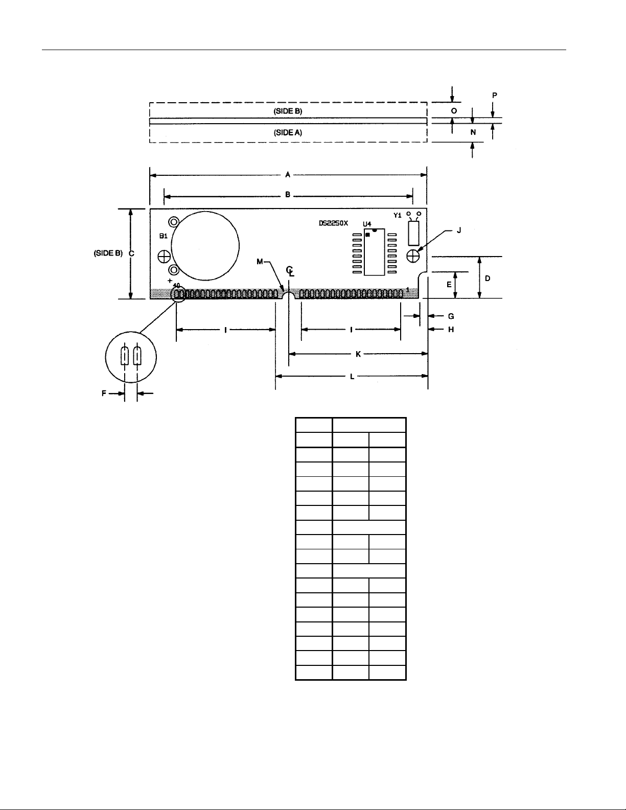
PACKAGE DRAWING
DS2250(T)
PKG INCHES
DIM MIN MAX
A 2.645 2.655
B 2.379 2.389
C 0.845 0.855
D 0.395 0.405
E 0.245 0.255
F 0.050 BSC
G 0.075 0.085
H 0.245 0.255
I 0.950 BSC
J 0.120 0.130
K 1.320 1.330
L 1.445 1.455
M 0.057 0.067
N - 0.160
O - 0.195
P 0.047 0.054
17 of 18
Page 18

DS2250(T)
DATA SHEET REVISION SUMMARY
The following represent the key differences between 12/13/95 and 08/16/96 version of the DS2250(T)
data sheet. Please review this summary carefully.
1. Correct Figure 3 to show RST active high.
2. Add minimum value to PCB thickness.
The following represent the key differences between 11/20/99 and 06/09/06 version of the DS2250(T)
data sheet. Please review this summary carefully.
1. Updated reference (Features) to 10-year NV RAM data life to include room temperature caveat.
2. Added lead-free package information to the Ordering Information table.
3. Removed 8kB package versions from Ordering Information table.
4. Removed references to “Secure Microcontroller Data Book” and changed them to “Secure
Microcontroller User’s Guide.”
5. Removed references to DS5000TK.
18 of 18
Maxim/Dallas Semiconductor cannot assume responsibility for use of any circuitry other than circuitry entirely embodied in a Maxim/Dallas Semiconductor product.
No circuit patent licenses are implied. Maxim/Dallas Semiconductor reserves the right to change the circuitry and specifications without notice at any time.
Maxim Integrated Products, 120 San Gabriel Drive, Sunnyvale, CA 94086 408-737-7600
The Maxim logo is a registered trademark of Maxim Integrated Products, Inc. The Dallas logo is a registered trademark of Dallas Semiconductor Corporation.
© 2006 Maxim Integrated Products • Printed USA
 Loading...