

Page 1
y
r
www.maxim-ic.com
GENERAL DESCRIPTION
The DS2155 is a software-selectable T1, E1, or J1
single-chip transceiver (SCT) for short-haul and
long-haul applications. The DS2155 is composed of
a line interface unit (LIU), framer, HDLC controllers,
and a TDM backplane interface, and is controlled by
an 8-bit parallel port configured for Intel or Motorola
bus operations. The DS2155 is pin and software
compatible with the DS2156.
The LIU is composed of transmit and receive
interfaces and a jitter attenuator. The transmit
interface is responsible for generating the necessary
waveshapes for driving the network and providing
the correct source impedance depending on the type
of media used. T1 waveform generation includes
DSX-1 line buildouts as well as CSU line buildouts
of -7.5dB, -15dB, and -22.5dB. E1 waveform
generation includes G.703 waveshapes for both 75
coax and 120 twisted cables. The receive interface
provides network termination and recovers clock and
data from the network.
APPLICATIONS
T1/E1/J1 Line Cards
Switches and Routers
Add-Drop Multiplexers
T1/E1/J1
NETWORK
DS2155
T1/E1/J1
SCT
BACKPLANE
TDM
T1/E1/J1 Single-Chip Transceive
DS2155
FEATURES
Complete T1/DS1/ISDN-PRI/J1 Transceiver
Functionality
Complete E1 (CEPT) PCM-30/ISDN-PRI
Transceiver Functionality
Long-Haul and Short-Haul Line Interface for
Clock/Data Recovery and Waveshaping
CMI Coder/Decoder for Optical I/F
Crystal-Less Jitter Attenuator
Fully Independent Transmit and Receive
Functionality
Dual HDLC Controllers
Programmable BERT Generator and Detector
Internal Software-Selectable Receive and
Transmit-Side Termination Resistors for
75/100/120 T1 and E1 Interfaces
Dual Two-Frame Elastic-Store Slip Buffers that
Connect to Asynchronous Backplanes Up to
16.384MHz
16.384MHz, 8.192MHz, 4.096MHz, or
2.048MHz Clock Output Synthesized to
Recovered Network Clock
Features continued on page 2.
ORDERING INFORMATION
PART TEMP RANGE PIN-PACKAGE
DS2155L 0°C to +70°C
DS2155L+ 0°C to +70°C
DS2155LN -40°C to +85°C 100 LQFP
DS2155LN+ -40°C to +85°C 100 LQFP
DS2155G 0°C to +70°C
DS2155G+ 0°C to +70°C
DS2155GN -40°C to +85°C 100 CSBGA
DS2155GN -40°C to +85°C 100 CSBGA
+ Denotes lead-free/RoHS-compliant package.
100 LQFP
100 LQFP
100 CSBGA
100 CSBGA
Note: Some revisions of this device may incorporate deviations from published specifications known as errata. Multiple revisions of any device
be simultaneously available through various sales channels. For information about device errata, click here: www.maxim-ic.com/errata.
ma
1 of 238 REV: 040907
Page 2

DS2155
1. TABLE OF CONTENTS
1. TABLE OF CONTENTS ............................................................................................................................2
1.1 TABLE OF FIGURES ........................................................................................................................................6
1.2 TABLE OF TABLES..........................................................................................................................................7
2. DATA SHEET REVISION HISTORY .....................................................................................................8
3. MAIN FEATURES....................................................................................................................................10
3.1 FUNCTIONAL DESCRIPTION .........................................................................................................................13
3.2 BLOCK DIAGRAM.........................................................................................................................................15
4. PIN FUNCTION DESCRIPTION ...........................................................................................................19
4.1 TRANSMIT SIDE ...........................................................................................................................................19
4.2 RECEIVE SIDE ..............................................................................................................................................21
4.3 PARALLEL CONTROL PORT PINS .................................................................................................................24
4.4 EXTENDED SYSTEM INFORMATION BUS......................................................................................................25
4.5 USER OUTPUT PORT PINS ............................................................................................................................26
4.6 JTAG TEST ACCESS PORT PINS...................................................................................................................27
4.7 LINE INTERFACE PINS ..................................................................................................................................28
4.8 SUPPLY PINS ................................................................................................................................................29
4.9 L AND G PACKAGE PINOUT .........................................................................................................................30
4.10 10MM CSBGA PIN CONFIGURATION ......................................................................................................32
5. PARALLEL PORT ...................................................................................................................................33
5.1 REGISTER MAP ............................................................................................................................................33
6. PROGRAMMING MODEL.....................................................................................................................39
6.1 POWER-UP SEQUENCE .................................................................................................................................40
6.1.1 Master Mode Register.........................................................................................................................40
6.2 INTERRUPT HANDLING ................................................................................................................................41
6.3 STATUS REGISTERS......................................................................................................................................41
6.4 INFORMATION REGISTERS ...........................................................................................................................42
6.5 INTERRUPT INFORMATION REGISTERS ........................................................................................................42
7. SPECIAL PER-CHANNEL REGISTER OPERATION.......................................................................43
8. CLOCK MAP ............................................................................................................................................45
9. T1 FRAMER/FORMATTER CONTROL AND STATUS REGISTERS............................................46
9.1 T1 CONTROL REGISTERS .............................................................................................................................46
9.2 T1 TRANSMIT TRANSPARENCY ...................................................................................................................51
9.3 AIS-CI AND RAI-CI GENERATION AND DETECTION ..................................................................................51
9.4 T1 RECEIVE-SIDE DIGITAL-MILLIWATT CODE GENERATION .....................................................................52
10. E1 FRAMER/FORMATTER CONTROL AND STATUS REGISTERS............................................55
10.1 E1 CONTROL REGISTERS.........................................................................................................................55
10.2 AUTOMATIC ALARM GENERATION .........................................................................................................59
10.3 E1 INFORMATION REGISTERS..................................................................................................................60
11. COMMON CONTROL AND STATUS REGISTERS ..........................................................................62
11.1 T1/E1 STATUS REGISTERS ......................................................................................................................63
2 of 238
Page 3

DS2155
12. I/O PIN CONFIGURATION OPTIONS.................................................................................................69
13. LOOPBACK CONFIGURATION ..........................................................................................................71
13.1 PER-CHANNEL LOOPBACK ......................................................................................................................73
14. ERROR COUNT REGISTERS ...............................................................................................................75
14.1 LINE-CODE VIOLATION COUNT REGISTER (LCVCR).............................................................................76
14.1.1 T1 Operation.......................................................................................................................................76
14.1.2 E1 Operation.......................................................................................................................................76
14.2 PATH CODE VIOLATION COUNT REGISTER (PCVCR) ............................................................................78
14.2.1 T1 Operation.......................................................................................................................................78
14.2.2 E1 Operation.......................................................................................................................................78
14.3 FRAMES OUT-OF-SYNC COUNT REGISTER (FOSCR)..............................................................................79
14.3.1 T1 Operation.......................................................................................................................................79
14.3.2 E1 Operation.......................................................................................................................................79
14.4 E-BIT COUNTER (EBCR).........................................................................................................................80
15. DS0 MONITORING FUNCTION ...........................................................................................................81
16. SIGNALING OPERATION .....................................................................................................................83
16.1 RECEIVE SIGNALING ...............................................................................................................................83
16.1.1 Processor-Based Signaling.................................................................................................................83
16.1.2 Hardware-Based Receive Signaling ...................................................................................................84
16.2 TRANSMIT SIGNALING.............................................................................................................................89
16.2.1 Processor-Based Mode .......................................................................................................................89
16.2.2 Software Signaling Insertion-Enable Registers, E1 CAS Mode..........................................................93
16.2.3 Software Signaling Insertion-Enable Registers, T1 Mode..................................................................95
16.2.4 Hardware-Based Mode.......................................................................................................................95
17. PER-CHANNEL IDLE CODE GENERATION ....................................................................................96
17.1 IDLE-CODE PROGRAMMING EXAMPLES ..................................................................................................97
18. CHANNEL BLOCKING REGISTERS ................................................................................................101
19. ELASTIC STORES OPERATION........................................................................................................104
19.1 RECEIVE SIDE ........................................................................................................................................107
19.1.1 T1 Mode ............................................................................................................................................107
19.1.2 E1 Mode............................................................................................................................................107
19.2 TRANSMIT SIDE .....................................................................................................................................107
19.2.1 T1 Mode ............................................................................................................................................108
19.2.2 E1 Mode............................................................................................................................................108
19.3 ELASTIC STORES INITIALIZATION .........................................................................................................108
19.4 MINIMUM DELAY MODE .......................................................................................................................108
20. G.706 INTERMEDIATE CRC-4 UPDATING (E1 MODE ONLY)...................................................109
21. T1 BIT-ORIENTED CODE (BOC) CONTROLLER..........................................................................110
21.1 TRANSMIT BOC.....................................................................................................................................110
Transmit a BOC ..............................................................................................................................................110
21.2 RECEIVE BOC .......................................................................................................................................110
Receive a BOC.................................................................................................................................................110
22. ADDITIONAL (SA) AND INTERNATIONAL (SI) BIT OPERATION (E1 ONLY) ......................113
3 of 238
Page 4

DS2155
22.1 METHOD 1: HARDWARE SCHEME .........................................................................................................113
22.2 METHOD 2: INTERNAL REGISTER SCHEME BASED ON DOUBLE-FRAME ..............................................113
22.3 METHOD 3: INTERNAL REGISTER SCHEME BASED ON CRC4 MULTIFRAME........................................116
23. HDLC CONTROLLERS ........................................................................................................................126
23.1 BASIC OPERATION DETAILS ..................................................................................................................126
23.2 HDLC CONFIGURATION........................................................................................................................126
23.2.1 FIFO Control....................................................................................................................................130
23.3 HDLC MAPPING....................................................................................................................................131
23.3.1 Receive ..............................................................................................................................................131
23.3.2 Transmit ............................................................................................................................................133
23.3.3 FIFO Information .............................................................................................................................138
23.3.4 Receive Packet-Bytes Available ........................................................................................................138
23.3.5 HDLC FIFOs ....................................................................................................................................139
23.4 RECEIVE HDLC CODE EXAMPLE..........................................................................................................140
23.5 LEGACY FDL SUPPORT (T1 MODE)......................................................................................................140
23.5.1 Overview ...........................................................................................................................................140
23.5.2 Receive Section .................................................................................................................................140
23.5.3 Transmit Section ...............................................................................................................................142
23.6 D4/SLC-96 OPERATION ........................................................................................................................142
24. LINE INTERFACE UNIT (LIU) ...........................................................................................................143
24.1 LIU OPERATION ....................................................................................................................................143
24.2 RECEIVER ..............................................................................................................................................143
24.2.1 Receive Level Indicator and Threshold Interrupt .............................................................................144
24.2.2 Receive G.703 Synchronization Signal (E1 Mode)...........................................................................144
24.2.3 Monitor Mode ...................................................................................................................................144
24.3 TRANSMITTER .......................................................................................................................................145
24.3.1 Transmit Short-Circuit Detector/Limiter ..........................................................................................145
24.3.2 Transmit Open-Circuit Detector.......................................................................................................145
24.3.3 Transmit BPV Error Insertion ..........................................................................................................145
24.3.4 Transmit G.703 Synchronization Signal (E1 Mode).........................................................................145
24.4 MCLK PRESCALER ...............................................................................................................................146
24.5 JITTER ATTENUATOR.............................................................................................................................146
24.6 CMI (CODE MARK INVERSION) OPTION ...............................................................................................146
24.7 LIU CONTROL REGISTERS.....................................................................................................................147
24.8 RECOMMENDED CIRCUITS.....................................................................................................................156
24.9 COMPONENT SPECIFICATIONS ...............................................................................................................158
25. PROGRAMMABLE IN-BAND LOOP CODE GENERATION AND DETECTION......................163
26. BERT FUNCTION ..................................................................................................................................170
26.1 STATUS ..................................................................................................................................................170
26.2 MAPPING ...............................................................................................................................................170
26.3 BERT REGISTER DESCRIPTIONS ...........................................................................................................172
26.4 BERT REPETITIVE PATTERN SET..........................................................................................................176
26.5 BERT BIT COUNTER .............................................................................................................................177
26.6 BERT ERROR COUNTER........................................................................................................................178
27. PAYLOAD ERROR-INSERTION FUNCTION (T1 MODE ONLY)................................................180
27.1 NUMBER-OF-ERRORS REGISTERS..........................................................................................................182
27.1.1 Number-of-Errors Left Register........................................................................................................183
28. INTERLEAVED PCM BUS OPERATION (IBO)...............................................................................184
4 of 238
Page 5

DS2155
28.1 CHANNEL INTERLEAVE .........................................................................................................................184
28.2 FRAME INTERLEAVE..............................................................................................................................184
29. EXTENDED SYSTEM INFORMATION BUS (ESIB) .......................................................................187
30. PROGRAMMABLE BACKPLANE CLOCK SYNTHESIZER ........................................................191
31. FRACTIONAL T1/E1 SUPPORT .........................................................................................................191
32. USER-PROGRAMMABLE OUTPUT PINS........................................................................................193
33. TRANSMIT FLOW DIAGRAMS .........................................................................................................194
34. JTAG BOUNDARY SCAN ARCHITECTURE AND TEST ACCESS PORT .................................199
34.1 DESCRIPTION .........................................................................................................................................199
34.2 INSTRUCTION REGISTER........................................................................................................................202
34.3 TEST REGISTERS....................................................................................................................................204
34.4 BOUNDARY SCAN REGISTER .................................................................................................................204
34.5 BYPASS REGISTER .................................................................................................................................204
34.6 IDENTIFICATION REGISTER....................................................................................................................204
35. FUNCTIONAL TIMING DIAGRAMS.................................................................................................208
35.1 T1 MODE ...............................................................................................................................................208
35.2 E1 MODE ...............................................................................................................................................213
36. OPERATING PARAMETERS ..............................................................................................................222
37. AC TIMING PARAMETERS AND DIAGRAMS ...............................................................................224
37.1 MULTIPLEXED BUS AC CHARACTERISTICS ..........................................................................................224
37.2 NONMULTIPLEXED BUS AC CHARACTERISTICS ...................................................................................227
37.3 RECEIVE-SIDE AC CHARACTERISTICS ..................................................................................................230
37.4 BACKPLANE CLOCK TIMING: AC CHARACTERISTICS .........................................................................233
37.5 TRANSMIT AC CHARACTERISTICS ........................................................................................................234
38. PACKAGE INFORMATION ................................................................................................................237
38.1 100-PIN LQFP (56-G5002-000) ............................................................................................................237
38.2 100-BALL CSBGA (56-G6008-001) .....................................................................................................238
5 of 238
Page 6

DS2155
1.1 Table of Figures
Figure 3-1. Block Diagram........................................................................................................................................ 15
Figure 3-2. Receive and Transmit LIU...................................................................................................................... 16
Figure 3-3. Receive and Transmit Framer/HDLC..................................................................................................... 17
Figure 3-4. Backplane Interface ................................................................................................................................ 18
Figure 4-1. 10mm CSBGA Pin Configuration .......................................................................................................... 32
Figure 6-1. Programming Sequence .......................................................................................................................... 39
Figure 8-1. Clock Map............................................................................................................................................... 45
Figure 16-1. Simplified Diagram of Receive Signaling Path .................................................................................... 83
Figure 16-2. Simplified Diagram of Transmit Signaling Path................................................................................... 89
Figure 20-1. CRC-4 Recalculate Method ................................................................................................................ 109
Figure 24-1. Typical Monitor Application .............................................................................................................. 144
Figure 24-2. CMI Coding ........................................................................................................................................ 146
Figure 24-3. Software-Selected Termination, Metallic Protection.......................................................................... 156
Figure 24-4. Software-Selected Termination, Longitudinal Protection................................................................... 157
Figure 24-5. E1 Transmit Pulse Template............................................................................................................... 159
Figure 24-6. T1 Transmit Pulse Template............................................................................................................... 159
Figure 24-7. Jitter Tolerance.................................................................................................................................... 160
Figure 24-8. Jitter Tolerance (E1 Mode) ................................................................................................................. 160
Figure 24-9. Jitter Attenuation (T1 Mode) .............................................................................................................. 161
Figure 24-10. Jitter Attenuation (E1 Mode) ............................................................................................................ 161
Figure 24-11. Optional Crystal Connections ........................................................................................................... 162
Figure 26-1. Simplified Diagram of BERT in Network Direction .......................................................................... 171
Figure 26-2. Simplified Diagram of BERT in Backplane Direction ....................................................................... 171
Figure 28-1. IBO Example ...................................................................................................................................... 186
Figure 29-1. ESIB Group of Four DS2155s ............................................................................................................ 187
Figure 33-1. T1 Transmit Flow Diagram ................................................................................................................ 194
Figure 33-2. E1 Transmit Flow Diagram ................................................................................................................ 195
Figure 34-1. JTAG Functional Block Diagram ....................................................................................................... 199
Figure 34-2. TAP Controller State Diagram............................................................................................................ 202
Figure 35-1. Receive-Side D4 Timing..................................................................................................................... 208
Figure 35-2. Receive-Side ESF Timing................................................................................................................... 208
Figure 35-3. Receive-Side Boundary Timing (Elastic Store Disabled)................................................................... 209
Figure 35-4. Receive-Side 1.544MHz Boundary Timing (Elastic Store Enabled).................................................. 209
Figure 35-5. Receive-Side 2.048MHz Boundary Timing (Elastic Store Enabled).................................................. 210
Figure 35-6. Transmit-Side D4 Timing................................................................................................................... 210
Figure 35-7. Transmit-Side ESF Timing................................................................................................................. 211
Figure 35-8. Transmit-Side Boundary Timing (with Elastic Store Disabled)......................................................... 211
Figure 35-9. Transmit-Side 1.544MHz Boundary Timing (Elastic Store Enabled)................................................ 212
Figure 35-10. Transmit-Side 2.048MHz Boundary Timing (Elastic Store Enabled).............................................. 212
Figure 35-11. Receive-Side Timing ........................................................................................................................ 213
Figure 35-12. Receive-Side Boundary Timing (with Elastic Store Disabled)......................................................... 213
Figure 35-13. Receive-Side Boundary Timing, RSYSCLK = 1.544MHz (Elastic Store Enabled) ........................ 214
Figure 35-14. Receive-Side Boundary Timing, RSYSCLK = 2.048MHz (Elastic Store Enabled) ........................ 214
Figure 35-15. Receive IBO Channel Interleave Mode Timing ............................................................................... 215
Figure 35-16. Receive IBO Frame Interleave Mode Timing................................................................................... 216
Figure 35-17. G.802 Timing, E1 Mode Only .......................................................................................................... 217
Figure 35-18. Transmit-Side Timing....................................................................................................................... 217
Figure 35-19. Transmit-Side Boundary Timing (Elastic Store Disabled) ............................................................... 218
Figure 35-20. Transmit-Side Boundary Timing, TSYSCLK = 1.544MHz (Elastic Store Enabled) ...................... 218
Figure 35-21. Transmit-Side Boundary Timing, TSYSCLK = 2.048MHz (Elastic Store Enabled) ....................... 219
Figure 35-22. Transmit IBO Channel Interleave Mode Timing.............................................................................. 220
6 of 238
Page 7

DS2155
Figure 35-23. Transmit IBO Frame Interleave Mode Timing................................................................................. 221
Figure 37-1. Intel Multiplexed Bus Read Timing (BTS = 0/MUX = 1).................................................................. 225
Figure 37-2. Intel Multiplexed Bus Write Timing (BTS = 0/MUX = 1)................................................................. 225
Figure 37-3. Motorola Multiplexed Bus Timing (BTS = 1/MUX = 1) ................................................................... 226
Figure 37-4. Intel Nonmultiplexed Bus Read Timing (BTS = 0/MUX = 0) ........................................................... 228
Figure 37-5. Intel Nonmultiplexed Bus Write Timing (BTS = 0/MUX = 0) .......................................................... 228
Figure 37-6. Motorola Nonmultiplexed Bus Read Timing (BTS = 1/MUX = 0).................................................... 229
Figure 37-7. Motorola Nonmultiplexed Bus Write Timing (BTS = 1/MUX = 0)................................................... 229
Figure 37-8. Receive-Side Timing .......................................................................................................................... 231
Figure 37-9. Receive-Side Timing, Elastic Store Enabled ...................................................................................... 232
Figure 37-10. Receive Line Interface Timing ......................................................................................................... 232
Figure 37-11 Receive Timing Delay RCLK to BPCLK......................................................................................... 233
Figure 37-12. Transmit-Side Timing....................................................................................................................... 235
Figure 37-13. Transmit-Side Timing, Elastic Store Enabled................................................................................... 236
Figure 37-14. Transmit Line Interface Timing........................................................................................................ 236
1.2 Table of Tables
Table 4-A. Pin Description Sorted by Pin Number ................................................................................................... 30
Table 5-A. Register Map Sorted by Address............................................................................................................. 33
Table 9-A. T1 Alarm Criteria .................................................................................................................................... 54
Table 10-A. E1 Sync/Resync Criteria ....................................................................................................................... 56
Table 10-B. E1 Alarm Criteria .................................................................................................................................. 61
Table 14-A. T1 Line Code Violation Counting Options ........................................................................................... 76
Table 14-B. E1 Line-Code Violation Counting Options ........................................................................................... 76
Table 14-C. T1 Path Code Violation Counting Arrangements.................................................................................. 78
Table 14-D. T1 Frames Out-of-Sync Counting Arrangements ................................................................................. 79
Table 16-A. Time Slot Numbering Schemes............................................................................................................. 90
Table 17-A. Idle-Code Array Address Mapping ....................................................................................................... 96
Table 17-B. GRIC and GTIC Functions.................................................................................................................... 98
Table 19-A. Elastic Store Delay After Initialization ............................................................................................... 108
Table 23-A. HDLC Controller Registers................................................................................................................. 127
Table 24-A. Component List (Software-Selected Termination, Metallic Protection)............................................. 156
Table 24-B. Component List (Software-Selected Termination, Longitudinal Protection)...................................... 157
Table 24-C. Transformer Specifications.................................................................................................................. 158
Table 27-A. Transmit Error-Insertion Setup Sequence ........................................................................................... 180
Table 27-B. Error Insertion Examples..................................................................................................................... 182
Table 34-A. Instruction Codes for IEEE 1149.1 Architecture ................................................................................ 203
Table 34-B. ID Code Structure................................................................................................................................ 204
Table 34-C. Device ID Codes.................................................................................................................................. 204
Table 34-D. Boundary Scan Control Bits................................................................................................................ 205
7 of 238
Page 8

DS2155
2. DATA SHEET REVISION HISTORY
REVISION DESCRIPTION
040907 Added Note 1 (GBD for cold temp) to Absolute Maximum Ratings (Section 36).
041806 Replaced Figure 24-3 and Figure 24-4, added Table 24-A and Table 24-B.
011606 Added lead-free packages to Ordering Information table on page 1.
100903
Add revision history table: The previous version of the DS2155 data sheet (12-06-02) did
not incorporate a revision history table and did not describe new features added to B1
revision of the DS2155.
THE FOLLOWING WERE INADVERTENTLY REMOVED FROM THE
PREVIOUS VERSION OF THE DS2155 DATA SHEET:
Add CSBGA package information to Ordering Information table on front page
Add CSBGA package thermal characteristics to Operating Parameters section
Add Transmit Line Build Out Control register (TLBC) description
Add Transmit Line Build Out Control register (TLBC) to Port Map
Add Transmit Line Build Out Control register (TLBC) description to LIU TRANSMIT
section
THE FOLLOWING ARE CORRECTIONS TO ERRORS IN THE PREVIOUS
VERSION OF THE DS2155 DATA SHEET:
Correct Device ID in Device Identification Register
Correct Device ID in JTAG ID Code table
Correct minimum value for t
PARALLEL PORT table. t
Correct minimum value for t
PARALLEL PORT table. t
in AC CHARACTERISTICS: MULTIPLEXED
DHW
was changed from 5ns to 0ns
DHW
in AC CHARACTERISTICS: MULTIPLEXED
DDR
was changed from unstated to 20ns
DDR
Corrections to AC CHARACTERISTICS: TRANSMIT SIDE timing table.
1. tCP, tCH, tCL, tLP, tLH, tLL, and tSP typical values have been restated to reflect various IBO
modes.
, t
2. t
CH
3. t
, t
SP
LL
minimum values have been changed from 75ns to 22ns.
4. t
D3
, t
CL, tLH
minimum values have been changed from 75ns to 20ns.
LL
minimum values have been changed from 50ns to 20ns.
Corrections to AC CHARACTERISTICS: RECEIVE SIDE timing table.
1. tCP, tCH, tCL, tLP, tLH, tLL, and tSP typical values have been restated to reflect various IBO
modes.
2. t
, t
CH
3. tSH, t
4. t
SH
5. t
D3, tD4
minimum values have been changed from 75ns to 20ns.
CL,
minimum values have been changed from 50ns to 20ns.
SL
, t
typical values have been added.
SL
minimum values have been changed from 50ns to 22ns.
Correct Transmit Signaling Registers (E1 Mode, CCS Format) table in Transmit Signaling
section
The definition of the EGL bit in the LIC1 register has been corrected for both T1 and E1
mode.
T1 Mode: EGL = 1 was changed from 15dB to –15dB
E1 Mode: EGL = 0 was changed from –10dB to –12dB
8 of 238
Page 9

DS2155
REVISION DESCRIPTION
THE FOLLOWING ARE FORMAT CHANGES AND ADDED OR REMOVED
TEXT, TABLES OR DIAGRAMS:
Replace X* format for showing active low signals with X
Remove redundant statements about “multiport configurations” in Interrupt Handling
section
Remove BASIC NETWORK CONNECTIONS figure in LINE INTERFACE UNIT
section
Add “Simplified Diagram of BERT in Network Direction” figure to BERT section
Add “Simplified Diagram of BERT in Backplane Direction” figure to BERT section
Add Receive Signaling Registers (E1 Mode, CCS Format) table to Receive Signaling
section
Add GRIC and GTIC function table to IAAR register
Changed Table of contents to include table of figures and table of tables.
Add note for FASRC bit.
Add T1 and E1 Transmit Flow Chart.
Added RCLK to BPCLK timing diagram.
THE FOLLOWING ARE NEW FEATURES AVAILABLE ON THE DS2155 REV
B1 AND ARE EXPLAINED IN THE BODY OF THE DATA SHEET
Add FRAS0, TCCS, RCCS and GRSRE bits to Signaling Control Register (SIGCR)
Add section on AIS-CI and RAI-CI Generation and Detection
Add RAIS-CI status bit to Status Register 4 (SR4) and Interrupt Mask Register 4 (IMR4)
Add RAIS-CI status bit to Status Register 4 (SR4)
Add TRAI-CI control bit to T1 Common Control Register 1 (TCCR1)
Add TAIS-CI control bit to T1 Common Control Register 1 (TCCR1)
Add Pseudorandom 2E9-1 pattern to PS0, PS1 and PS2 bit description in Bert Control
Register 1 (BCR1)
Add BD bit to Information Register 2 (INFO2)
Add ILUT status bit to Status Register 1 (SR1) and Interrupt Mask Register 1 (IMR1)
Add INTDIS and TMSS bits to Common Control Register 3 (CCR3)
9 of 238
Page 10

DS2155
3. MAIN FEATURES
The DS2155 contains all of the features of the previous generation of Dallas Semiconductor’s T1 and E1 SCTs plus
many new features.
General
Programmable output clocks for fractional T1, E1,
H0, and H12 applications
Interleaving PCM bus operation
8-bit parallel control port, multiplexed or
nonmultiplexed, Intel or Motorola
IEEE 1149.1 JTAG-Boundary Scan
3.3V supply with 5V tolerant inputs and outputs
Pin compatible with DS2156, DS2152/DS2154,
and DS21x5Y SCT family
Signaling System 7 Support
RAI-CI, AIS-CI support
100-pin LQFP (14mm x 14mm) (DS2155L)
100-pin CSBGA (10mm x 10mm) (DS2155G)
3.3V supply with 5V tolerant inputs and outputs
Evaluation kits
IEEE 1149.1 JTAG boundary scan
Driver source code available from the factory
Line Interface
Requires only a 2.048MHz master clock for both
E1 and T1 operation with the option to use
1.544MHz for T1 operation
Fully software configurable
Short-haul and long-haul applications
Automatic receive sensitivity adjustments
Ranges include 0 to 43dB or 0 to 12dB for E1
applications and 0 to 13dB or 0 to 36dB for T1
applications
Receive level indication in 2.5dB steps from
-42.5dB to -2.5dB
Internal receive termination option for 75Ω, 100Ω,
and 120Ω lines
Internal transmit termination option for 75Ω, 100Ω,
and 120Ω lines
Monitor application gain settings of 20dB, 26dB,
and 32dB
G.703 receive synchronization-signal mode
Flexible transmit waveform generation
T1 DSX-1 line buildouts
T1 CSU line buildouts of -7.5dB, -15dB, and
-22.5dB
E1 waveforms include G.703 waveshapes for
both 75Ω coax and 120Ω twisted cables
AIS generation independent of loopbacks
Alternating ones and zeros generation
Square-wave output
Open-drain output option
NRZ format option
Transmitter power-down
Transmitter 50mA short-circuit limiter with
current-limit-exceeded indication
Transmit open-circuit-detected indication
Line interface function can be completely
decoupled from the framer/formatter
Clock Synthesizer
Output frequencies include 2.048MHz, 4.096MHz,
8.192MHz, and 16.384MHz
Derived from recovered receive clock
Jitter Attenuator
32-bit or 128-bit crystal-less jitter attenuator
Requires only a 2.048MHz master clock for both
E1 and T1 operation with the option to use
1.544MHz for T1 operation
Can be placed in either the receive or transmit path
or disabled
Limit trip indication
Framer/Formatter
Fully independent transmit and receive
functionality
Full receive and transmit path transparency
T1 framing formats include D4 (SLC-96) and ESF
Detailed alarm and status reporting with optional
interrupt support
Large path and line error counters for:
– T1: BPV, CV, CRC6, and framing bit errors
– E1: BPV, CV, CRC4, E-bit, and frame
alignment errors
Timed or manual update modes
DS1 idle code generation on a per-channel basis in
both transmit and receive paths
– User-defined
– Digital milliwatt
ANSI T1.403-1998 Support
RAI-CI detection and generation
AIS-CI detection and generation
E1ETS 300 011 RAI generation
G.965 V5.2 link detect
Ability to monitor one DS0 channel in both the
transmit and receive paths
In-band repeating pattern generators and detectors
– Three independent generators and detectors
– Patterns from 1 to 8 bits or 16 bits in length
RCL, RLOS, RRA, and RAIS alarms interrupt on
change-of-state
10 of 238
Page 11

Flexible signaling support
– Software or hardware based
– Interrupt generated on change of signaling data
– Receive signaling freeze on loss-of-sync,
carrier loss, or frame slip
Addition of hardware pins to indicate carrier loss
and signaling freeze
Automatic RAI generation to ETS 300 011
specifications
Access to Sa and Si bits
Option to extend carrier loss criteria to a 1ms
period as per ETS 300 233
Japanese J1 support
– Ability to calculate and check CRC6 according
to the Japanese standard
– Ability to generate Yellow Alarm according to
the Japanese standard
TDM Bus
Dual two-frame independent receive and transmit
elastic stores
– Independent control and clocking
– Controlled slip capability with status
– Minimum delay mode supported
16.384MHz maximum backplane burst rate
Supports T1 to CEPT (E1) conversion
Programmable output clocks for fractional T1, E1,
H0, and H12 applications
Interleaving PCM bus operation
Hardware signaling capability
– Receive signaling reinsertion to a backplane
multiframe sync
– Availability of signaling in a separate PCM
data stream
– Signaling freezing
Ability to pass the T1 F-bit position through the
elastic stores in the 2.048MHz backplane mode
Access to the data streams in between the
framer/formatter and the elastic stores
User-selectable synthesized clock output
HDLC Controllers
Two independent HDLC controllers
Fast load and unload features for FIFOs
SS7 support for FISU transmit and receive
Independent 128-byte Rx and Tx buffers with
interrupt support
Access FDL, Sa, or single/multiple DS0 channels
DS0 access includes Nx64 or Nx56
Compatible with polled or interrupt driven
environments
Bit-oriented code (BOC) support
DS2155
Test and Diagnostics
Programmable on-chip bit error-rate testing
Pseudorandom patterns including QRSS
User-defined repetitive patterns
Daly pattern
Error insertion single and continuous
Total bit and errored bit counts
Payload error insertion
Error insertion in the payload portion of the T1
frame in the transmit path
Errors can be inserted over the entire frame or
selected channels
Insertion options include continuous and absolute
number with selectable insertion rates
F-bit corruption for line testing
Loopbacks: remote, local, analog, and per-channel
loopback
Extended System Information Bus
Host can read interrupt and alarm status on up to 8
ports with a single bus read
User-Programmable Output Pins
Four user-defined output pins for controlling
external logic
Control Port
8-bit parallel control port
Multiplexed or nonmultiplexed buses
Intel or Motorola formats
Supports polled or interrupt environments
Software access to device ID and silicon revision
Software reset supported
– Automatic clear on power-up
Hardware reset pin
11 of 238
Page 12

The DS2155 is compliant with the following standards:
ANSI: T1.403-1995, T1.231–1993, T1.408
AT&T: TR54016, TR62411
ITU: G.703, G.704, G.706, G.736, G.775, G.823, G.932, I.431, O.151, Q.161
ITU-T: Recommendation I.432–03/93 B-ISDN User-Network Interface—Physical Layer
Specification
ETSI: ETS 300 011, ETS 300 166, ETS 300 233, CTR12, CTR4
Japanese: JTG.703, JTI.431, JJ-20.11 (CMI Coding Only)
DS2155
12 of 238
Page 13

DS2155
3.1 Functional Description
The DS2155 is a software-selectable T1, E1, or J1 single-chip transceiver (SCT) for short-haul and longhaul applications. The DS2155 is composed of an LIU, framer, HDLC controllers, and a TDM backplane
interface, and is controlled by an 8-bit parallel port configured for Intel or Motorola bus operations. The
DS2155 is pin and software compatible with the DS2156.
The LIU is composed of transmit and receive interfaces and a jitter attenuator. The transmit interface is
responsible for generating the necessary waveshapes for driving the network and providing the correct
source impedance depending on the type of media used. T1 waveform generation includes DSX-1 line
buildouts as well as CSU line buildouts of -7.5dB, -15dB, and -22.5dB. E1 waveform generation includes
G.703 waveshapes for both 75Ω coax and 120Ω twisted cables. The receive interface provides network
termination and recovers clock and data from the network. The receive sensitivity adjusts automatically to
the incoming signal and can be programmed for 0 to 43dB or 0 to 12dB for E1 applications and 0 to 30dB
or 0 to 36dB for T1 applications. The jitter attenuator removes phase jitter from the transmitted or
received signal. The crystal-less jitter attenuator requires only a 2.048MHz MCLK for both E1 and T1
applications (with the option of using a 1.544MHz MCLK in T1 applications) and can be placed in either
transmit or receive data paths. An additional feature of the LIU is a CMI coder/decoder for interfacing to
optical networks.
On the transmit side, clock, data, and frame-sync signals are provided to the framer by the backplane
interface section. The framer inserts the appropriate synchronization framing patterns, alarm information,
calculates and inserts the CRC codes, and provides the B8ZS/HDB3 (zero code suppression) and AMI
line coding. The receive-side framer decodes AMI, B8ZS, and HDB3 line coding, synchronizes to the
data stream, reports alarm information, counts framing/coding/CRC errors, and provides clock/data and
frame-sync signals to the backplane interface section.
Both the transmit and receive path have two HDLC controllers. The HDLC controllers transmit and
receive data through the framer block. The HDLC controllers can be assigned to any time slot, group of
time slots, portion of a time slot or to FDL (T1) or Sa bits (E1). Each controller has 128-byte FIFOs, thus
reducing the amount of processor overhead required to manage the flow of data. In addition, built-in
support for reducing the processor time is required in SS7 applications.
The backplane interface provides a versatile method of sending and receiving data from the host system.
Elastic stores provide a method for interfacing to asynchronous systems, converting from a T1/E1
network to a 2.048MHz, 4.096MHz, 8.192MHz, or N x 64kHz system backplane. The elastic stores also
manage slip conditions (asynchronous interface). An interleave bus option (IBO) is provided to allow up
to eight transceivers to share a high-speed backplane.
The parallel port provides access for control and configuration of the DS2155’s features. The extended
system information bus (ESIB) function allows up to eight transceivers to be accessed by a single read for
interrupt status or other user-selectable alarm status information. Diagnostic capabilities include
loopbacks, PRBS pattern generation/detection, and 16-bit loop-up and loop-down code generation and
detection.
13 of 238
Page 14

DS2155
Reader’s Note: This data sheet assumes a particular nomenclature of the T1 operating environment. In
each 125µs frame there are 24 8-bit channels plus a framing bit. It is assumed that the framing bit is sent
first followed by channel 1. Each channel is made up of eight bits that are numbered 1 to 8. Bit number 1
is the MSB and is transmitted first. Bit number 8 is the LSB and is transmitted last. The term “locked” is
used to refer to two clock signals that are phase- or frequency-locked or derived from a common clock
(i.e., a 1.544MHz clock can be locked to a 2.048MHz clock if they share the same 8kHz component).
Throughout this data sheet, the following abbreviations are used:
B8ZS Bipolar with 8 Zero Substitution
BOC Bit-Oriented Code
CRC Cyclical Redundancy Check
D4 Superframe (12 frames per multiframe) Multiframe Structure
ESF Extended Superframe (24 frames per multiframe) Multiframe Structure
FDL Facility Data Link
FPS Framing Pattern Sequence in ESF
Fs Signaling Framing Pattern in D4
Ft Terminal Framing Pattern in D4
HDLC High-Level Data Link Control
MF Multiframe
SLC–96 Subscriber Loop Carrier—96 Channels
14 of 238
Page 15
DS2155
3.2 Block Diagram
Figure 3-1 shows a simplified block diagram featuring the major components of the DS2155. Details are
shown in subsequent figures. The block diagram is divided into three functional blocks: LIU, FRAMER,
and BACKPLANE INTERFACE.
Figure 3-1. Block Diagram
CLOCK
CLOCK
ADAPTER
EXTERNAL ACCESS
TO RECEIVE SIGNALS
RX
LIU
MUX
HDB3 / B8ZS
SYNC
SINGALING
ALARM DET
HDLCs
BACKPLANE
CLOCK SYNTH
BACKPLANE
INTERFACE
T1/E1/J1
NETWORK
TX
LIU
LIU
LOCAL LOOPBACK
JITTER ATTENUATOR
EXTERNAL ACCESS
TO TRANSMIT SIGNALS
REMOTE LOOPBACK
MUX
FRAMER LOOPBACK
FRAMER
SINGALING
ALARM GEN
HDLCs
CRC GEN
HDB3 / B8ZS
PAYLOAD LOOPBACK
FRAMER BACKPLANE
CIRCUIT
BACKPLANE
INTERFACE
JTAG ESIB
HOST INTERFACE
15 of 238
Page 16
Figure 3-2. Receive and Transmit LIU
8XCLK
XTALD
MCLK
DS2155
RPOSO
RNEGO
RCLKO
RNEGI
RPOSI
RCLKI
RCL
RRING
RTIP
TRING
TTIP
VCO / PLL
32.768MHz
RECEIVE
LINE I/F
LOCAL LOOPBACK
TRANSMIT
LINE I/F
JITTER ATTENUATOR
OR RECEIVE PATH
TRANSMIT
MUX
TPOSI
LIUC
TCLKI
MUX
REMOTE LOOPBACK
TNEGO
TNEGI
TPOSO
TCLKO
JACLK
RPOS
RNEG
RCLK
TPOS
TNEG
TCLK
16 of 238
Page 17
Figure 3-3. Receive and Transmit Framer/HDLC
REC
HDLC #1
128 Byte
FIFO
REC
HDLC #2
128 Byte
FIFO
DS2155
RPOS
RNEG
RCLK
TPOS
TNEG
TCLK
DATA
FRAMER LOOPBACK
RECEIVE
FRAMER
TRANSMIT
FRAMER
CLOCK
SYNC
SYNC
CLOCK
DATA
MAPPER MAPPER
MAPPER
XMIT
HDLC #1
128 Byte
FIFO
MAPPER
XMIT
HDLC #2
128 Byte
FIFO
PAYLOAD LOOPBACK
DATA
CLOCK
SYNC
SYNC
CLOCK
DATA
17 of 238
Page 18
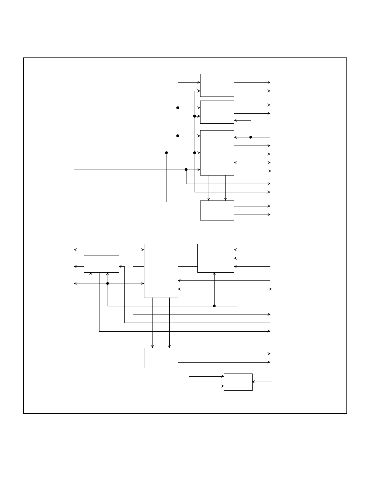
Figure 3-4. Backplane Interface
DS2155
DATA
CLOCK
Sa BIT/FDL
EXTRACTION
SIGNALING
BUFFER
ELASTIC
STORE
RLINK
RLCLK
RSIG
RSIGFR
RSYSCLK
RSER
RCLK
RSYNC
SYNC
RMSYNC
RFSYNC
RDATA
RCHCLK
RCHBLK
TSER
TSIG
TSSYNC
SYNC
DATA
Sa/FDL
INSERT
ELASTIC
STORE
CHANNEL
TIMING
SIGNALING
BUFFER
CLOCK
JACLK
CHANNEL
TIMING
TCLK
MUX
TSYSCLK
TSYNC
TESO
TDATA
TLCLK
TLINK
TCHCLK
TCHBLK
TCLK
18 of 238
Page 19

DS2155
4. PIN FUNCTION DESCRIPTION
4.1 Transmit Side
Signal Name:
Signal Description:
Signal Type:
A 1.544MHz (T1) or a 2.048MHz (E1) primary clock. Used to clock data through the transmit-side formatter.
TCLK can be internally sourced from MCLK. This is the most flexible method and requires only a single clock
signal for both T1 or E1. If internal sourcing is used, then the TCLK pin should be connected low.
Signal Name:
Signal Description:
Signal Type:
Transmit NRZ serial data. Sampled on the falling edge of TCLK when the transmit-side elastic store is disabled.
Sampled on the falling edge of TSYSCLK when the transmit-side elastic store is enabled.
Signal Name:
Signal Description:
Signal Type:
A 192kHz (T1) or 256kHz (E1) clock that pulses high during the LSB of each channel. Can also be programmed to
output a gated transmit bit clock on a per-channel basis. Synchronous with TCLK when the transmit-side elastic
store is disabled. Synchronous with TSYSCLK when the transmit-side elastic store is enabled. Useful for parallelto-serial conversion of channel data.
Signal Name:
Signal Description:
Signal Type:
A user-programmable output that can be forced high or low during any of the channels. Synchronous with TCLK
when the transmit-side elastic store is disabled. Synchronous with TSYSCLK when the transmit-side elastic store is
enabled. Useful for blocking clocks to a serial UART or LAPD controller in applications where not all channels are
used such as Fractional T1, Fractional E1, 384kbps (H0), 768kbps, or ISDN–PRI. Also useful for locating
individual channels in drop-and-insert applications, for external per-channel loopback, and for per-channel
conditioning.
Signal Name:
Signal Description:
Signal Type:
1.544MHz, 2.048MHz, 4.096MHz, 8.192MHz, or 16.384MHz clock. Only used when the transmit-side elastic
store function is enabled. Should be connected low in applications that do not use the transmit-side elastic store.
See Section 28
Signal Name:
Signal Description:
Signal Type:
Demand clock for the transmit link data [TLINK] input.
T1 Mode: A 4kHz or 2kHz (ZBTSI) clock.
E1 Mode: A 4kHz to 20kHz clock.
for details on 4.096MHz, 8.192MHz, and 16.384MHz operation using the IBO.
TCLK
Transmit Clock
Input
TSER
Transmit Serial Data
Input
TCHCLK
Transmit Channel Clock
Output
TCHBLK
Transmit Channel Block
Output
TSYSCLK
Transmit System Clock
Input
TLCLK
Transmit Link Clock
Output
19 of 238
Page 20

DS2155
Signal Name:
Signal Description:
Signal Type:
If enabled, this pin is sampled on the falling edge of TCLK for data insertion into either the FDL stream (ESF) or
the Fs-bit position (D4), or the Z-bit position (ZBTSI) or any combination of the Sa-bit positions (E1).
Signal Name:
Signal Description:
Signal Type:
A pulse at this pin establishes either frame or multiframe boundaries for the transmit side. Can be programmed to
output either a frame or multiframe pulse. If this pin is set to output pulses at frame boundaries, it can also be set by
IOCR1.3 to output double-wide pulses at signaling frames in T1 mode.
Signal Name:
Signal Description:
Signal Type:
Only used when the transmit-side elastic store is enabled. A pulse at this pin establishes either frame or multiframe
boundaries for the transmit side. Should be connected low in applications that do not use the transmit-side elastic
store.
Signal Name:
Signal Description:
Signal Type:
When enabled, this input samples signaling bits for insertion into outgoing PCM data stream. Sampled on the
falling edge of TCLK when the transmit-side elastic store is disabled. Sampled on the falling edge of TSYSCLK
when the transmit-side elastic store is enabled.
Signal Name:
Signal Description:
Signal Type:
Updated on the rising edge of TCLK with data out of the transmit-side elastic store whether the elastic store is
enabled or not. This pin is normally connected to TDATA.
Signal Name:
Signal Description:
Signal Type:
Sampled on the falling edge of TCLK with data to be clocked through the transmit-side formatter. This pin is
normally connected to TESO.
TLINK
Transmit Link Data
Input
TSYNC
Transmit Sync
Input/Output
TSSYNC
Transmit System Sync
Input
TSIG
Transmit Signaling Input
Input
TESO
Transmit Elastic Store Data Output
Output
TDATA
Transmit Data
Input
Signal Name:
Signal Description:
Signal Type:
Updated on the rising edge of TCLKO with the bipolar data out of the transmit-side formatter. Can be programmed
to source NRZ data by the output data format (IOCR1.0) control bit. This pin is normally connected to TPOSI.
Signal Name:
Signal Description:
Signal Type:
Updated on the rising edge of TCLKO with the bipolar data out of the transmit-side formatter. This pin is normally
connected to TNEGI.
Signal Name:
TPOSO
Transmit Positive-Data Output
Output
TNEGO
Transmit Negative-Data Output
Output
TCLKO
20 of 238
Page 21

DS2155
Signal Description:
Signal Type:
Transmit Clock Output
Output
Buffered clock that is used to clock data through the transmit-side formatter (i.e., either TCLK or RCLKI). This pin
is normally connected to TCLKI.
Signal Name:
Signal Description:
Signal Type:
TPOSI
Transmit Positive-Data Input
Input
Sampled on the falling edge of TCLKI for data to be transmitted out onto the T1 line. Can be internally connected
to TPOSO by connecting the LIUC pin high. TPOSI and TNEGI can be connected together in NRZ applications.
Signal Name:
Signal Description:
Signal Type:
TNEGI
Transmit Negative-Data Input
Input
Sampled on the falling edge of TCLKI for data to be transmitted out onto the T1 line. Can be internally connected
to TNEGO by connecting the LIUC pin high. TPOSI and TNEGI can be connected together in NRZ applications.
Signal Name:
Signal Description:
Signal Type:
TCLKI
Transmit Clock Input
Input
Line interface transmit clock. Can be internally connected to TCLKO by connecting the LIUC pin high.
4.2 Receive Side
Signal Name:
Signal Description:
Signal Type:
T1 Mode: Updated with either FDL data (ESF) or Fs bits (D4) or Z bits (ZBTSI) one RCLK before the start of a
frame.
E1 Mode: Updated with the full E1 data stream on the rising edge of RCLK.
Signal Name:
Signal Description:
Signal Type:
T1 Mode: A 4kHz or 2kHz (ZBTSI) clock for the RLINK output.
E1 Mode: A 4kHz to 20kHz clock.
Signal Name:
Signal Description:
Signal Type:
1.544MHz (T1) or 2.048MHz (E1) clock that is used to clock data through the receive-side framer.
Signal Name:
Signal Description:
Signal Type:
A 192kHz (T1) or 256kHz (E1) clock that pulses high during the LSB of each channel. Synchronous with RCLK
when the receive-side elastic store is disabled. Synchronous with RSYSCLK when the receive-side elastic store is
enabled. Useful for parallel-to-serial conversion of channel data.
RLINK
Receive Link Data
Output
RLCLK
Receive Link Clock
Output
RCLK
Receive Clock
Output
RCHCLK
Receive Channel Clock
Output
21 of 238
Page 22

DS2155
Signal Name:
Signal Description:
Signal Type:
RCHBLK
Receive Channel Block
Output
A user-programmable output that can be forced high or low during any of the 24 T1 or 32 E1 channels.
Synchronous with RCLK when the receive-side elastic store is disabled. Synchronous with RSYSCLK when the
receive-side elastic store is enabled. Useful for blocking clocks to a serial UART or LAPD controller in
applications where not all channels are used such as fractional service, 384kbps service, 768kbps, or ISDN–PRI.
Also useful for locating individual channels in drop-and-insert applications, for external per-channel loopback, and
for per-channel conditioning. See Section 18
Signal Name:
Signal Description:
Signal Type:
RSER
Receive Serial Data
Output
for details.
Received NRZ serial data. Updated on rising edges of RCLK when the receive-side elastic store is disabled.
Updated on the rising edges of RSYSCLK when the receive-side elastic store is enabled.
Signal Name:
Signal Description:
Signal Type:
RSYNC
Receive Sync
Input/Output
An extracted pulse, one RCLK wide, is output at this pin that identifies either frame (IOCR1.5 = 0) or multiframe
(IOCR1.5 = 1) boundaries. If set to output frame boundaries, then through IOCR1.6, RSYNC can also be set to
output double-wide pulses on signaling frames in T1 mode. If the receive-side elastic store is enabled, then this pin
can be enabled to be an input through IOCR1.4, at which a frame or multiframe boundary pulse is applied.
Signal Name:
Signal Description:
Signal Type:
RFSYNC
Receive Frame Sync
Output
An extracted 8kHz pulse, one RCLK wide, is output at this pin that identifies frame boundaries.
Signal Name:
Signal Description:
Signal Type:
An extracted pulse, one RCLK wide (elastic store disabled) or one RSYSCLK wide (elastic store enabled), is
output at this pin that identifies multiframe boundaries.
Signal Name:
Signal Description:
Signal Type:
Updated on the rising edge of RCLK with the data out of the receive-side framer.
Signal Name:
Signal Description:
Signal Type:
1.544MHz, 2.048MHz, 4.096MHz, or 8.192MHz clock. Only used when the receive-side elastic store function is
enabled. Should be connected low in applications that do not use the receive-side elastic store. See Section 28
details on 4.096MHz and 8.192MHz operation using the IBO.
Signal Name:
Signal Description:
Signal Type:
Outputs signaling bits in a PCM format. Updated on rising edges of RCLK when the receive-side elastic store is
disabled. Updated on the rising edges of RSYSCLK when the receive-side elastic store is enabled.
RMSYNC
Receive Multiframe Sync
Output
RDATA
Receive Data
Output
RSYSCLK
Receive System Clock
Input
for
RSIG
Receive Signaling Output
Output
22 of 238
Page 23

DS2155
Signal Name:
Signal Description:
Signal Type:
A dual function output that is controlled by the CCR1.0 control bit. This pin can be programmed to either toggle
high when the synchronizer is searching for the frame and multiframe or to toggle high if the TCLK pin has not
been toggled for 5µs.
Signal Name:
Signal Description:
Signal Type:
Set high when the line interface detects a carrier loss.
Signal Name:
Signal Description:
Signal Type:
Set high when the signaling data is frozen by either automatic or manual intervention. Used to alert downstream
equipment of the condition.
Signal Name:
Signal Description:
Signal Type:
A user-selectable synthesized clock output that is referenced to the clock that is output at the RCLK pin.
RLOS/LOTC
Receive Loss-of-Sync/Loss-of-Transmit Clock
Output
RCL
Receive Carrier Loss
Output
RSIGF
Receive Signaling Freeze
Output
BPCLK
Backplane Clock
Output
Signal Name:
Signal Description:
Signal Type:
Updated on the rising edge of RCLKO with bipolar data out of the line interface. This pin is normally connected to
RPOSI.
Signal Name:
Signal Description:
Signal Type:
Updated on the rising edge of RCLKO with the bipolar data out of the line interface. This pin is normally
connected to RNEGI.
Signal Name:
Signal Description:
Signal Type:
Buffered recovered clock from the network. This pin is normally connected to RCLKI.
Signal Name:
Signal Description:
Signal Type:
Sampled on the falling edge of RCLKI for data to be clocked through the receive-side framer. RPOSI and RNEGI
can be connected together for an NRZ interface. Can be internally connected to RPOSO by connecting the LIUC
pin high.
Signal Name:
Signal Description:
Signal Type:
Sampled on the falling edge of RCLKI for data to be clocked through the receive-side framer. RPOSI and RNEGI
can be connected together for an NRZ interface. Can be internally connected to RNEGO by connecting the LIUC
pin high.
RPOSO
Receive Positive-Data Output
Output
RNEGO
Receive Negative-Data Output
Output
RCLKO
Receive Clock Output
Output
RPOSI
Receive Positive-Data Input
Input
RNEGI
Receive Negative-Data Input
Input
23 of 238
Page 24

DS2155
Signal Name:
Signal Description:
Signal Type:
RCLKI
Receive Clock Input
Input
Clock used to clock data through the receive-side framer. This pin is normally connected to RCLKO. Can be
internally connected to RCLKO by connecting the LIUC pin high.
4.3 Parallel Control Port Pins
Signal Name:
Signal Description:
Signal Type:
Flags host controller during conditions and events defined in the status registers. Active-low, open-drain output.
Signal Name:
Signal Description:
Signal Type:
A dual function pin. A 0-to-1 transition issues a hardware reset to the DS2155 register set. A reset clears all
configuration registers. Configuration register contents are set to 0. Leaving TSTRST high tri-states all output and
I/O pins (including the parallel control port). Set low for normal operation. Useful in board-level testing.
Signal Name:
Signal Description:
Signal Type:
Set low to select nonmultiplexed bus operation. Set high to select multiplexed bus operation.
Signal Name:
Signal Description:
Signal Type:
In nonmultiplexed bus operation (MUX = 0), these serve as the data bus. In multiplexed bus operation (MUX = 1),
these pins serve as an 8-bit multiplexed address/data bus.
Signal Name:
Signal Description:
Signal Type:
In nonmultiplexed bus operation (MUX = 0), these serve as the address bus. In multiplexed bus operation
(MUX = 1), these pins are not used and should be connected low.
Signal Name:
Signal Description:
Signal Type:
Strap high to select Motorola bus timing; strap low to select Intel bus timing. This pin controls the function of the
RD (DS), ALE (AS), and WR (R/W) pins.
If BTS = 1, then these pins assume the function listed in parentheses ().
Signal Name:
Signal Description:
Signal Type:
In Intel mode, RD determines when data is read from the device. In Motorola mode, DS is used to write to the
device. See Bus Timing Diagrams.
INT
Interrupt
Output
TSTRST
Tri-State Control and Device Reset
Input
MUX
Bus Operation
Input
AD0 to AD7
Data Bus [D0 to D7] or Address/Data Bus
Input/Output
A0 to A6
Address Bus
Input
BTS
Bus Type Select
Input
RD (DS)
Read Input, Data Strobe
Input
24 of 238
Page 25

DS2155
Signal Name:
Signal Description:
Signal Type:
Must be low to read or write to the device. CS is an active-low signal.
Signal Name:
Signal Description:
Signal Type:
In nonmultiplexed bus operation (MUX = 0), serves as the upper address bit. In multiplexed bus operation
(MUX = 1), serves to demultiplex the bus on a positive-going edge.
Signal Name:
Signal Description:
Signal Type:
WR is an active-low signal.
CS
Chip Select
Input
ALE(AS)/A7
Address Latch Enable (Address Strobe) or A7
Input
WR (R/W)
Write Input(Read/Write)
Input
4.4 Extended System Information Bus
Signal Name:
Signal Description:
Signal Type:
Used to group two to eight DS2155s into a bus-sharing mode for alarm and status reporting. See Section 29
more details.
Signal Name:
Signal Description:
Signal Type:
Used to group two to eight DS2155s into a bus-sharing mode for alarm and status reporting. See Section 29
more details.
Signal Name:
Signal Description:
Signal Type:
Used to group two to eight DS2155s into a bus-sharing mode for alarm and status reporting. See Section 29
more details.
ESIBS0
Extended System Information Bus Select 0
Input/Output
for
ESIBS1
Extended System Information Bus Select 1
Input/Output
for
ESIBRD
Extended System Information Bus Read
Input/Output
for
25 of 238
Page 26

DS2155
4.5 User Output Port Pins
Signal Name:
Signal Description:
Signal Type:
This output port pin can be set low or high by the CCR4.0 control bit. This pin is forced low on power-up and after
any device reset.
Signal Name:
Signal Description:
Signal Type:
This output port pin can be set low or high by the CCR4.1 control bit. This pin is forced low on power-up and after
any device reset.
Signal Name:
Signal Description:
Signal Type:
This output port pin can be set low or high by the CCR4.2 control bit. This pin is forced low on power-up and after
any device reset.
Signal Name:
Signal Description:
Signal Type:
This output port pin can be set low or high by the CCR4.3 control bit. This pin is forced low on power-up and after
any device reset.
UOP0
User Output Port 0
Output
UOP1
User Output Port 1
Output
UOP2
User Output Port 2
Output
UOP3
User Output Port 3
Output
26 of 238
Page 27

DS2155
4.6 JTAG Test Access Port Pins
Signal Name:
Signal Description:
Signal Type:
JTRST is used to asynchronously reset the test access port controller. After power-up, JTRST must be toggled from
low to high. This action sets the device into the JTAG DEVICE ID mode. Normal device operation is restored by
pulling JTRST low. JTRST is pulled high internally by a 10kΩ resistor operation.
Signal Name:
Signal Description:
Signal Type:
This pin is sampled on the rising edge of JTCLK and is used to place the test access port into the various defined
IEEE 1149.1 states. This pin has a 10kΩ pullup resistor.
Signal Name:
Signal Description:
Signal Type:
This signal is used to shift data into JTDI on the rising edge and out of JTDO on the falling edge.
Signal Name:
Signal Description:
Signal Type:
Test instructions and data are clocked into this pin on the rising edge of JTCLK. This pin has a 10kΩ pullup
resistor.
Signal Name:
Signal Description:
Signal Type:
Test instructions and data are clocked out of this pin on the falling edge of JTCLK. If not used, this pin should be
left unconnected.
JTRST
IEEE 1149.1 Test Reset
Input
JTMS
IEEE 1149.1 Test Mode Select
Input
JTCLK
IEEE 1149.1 Test Clock Signal
Input
JTDI
IEEE 1149.1 Test Data Input
Input
JTDO
IEEE 1149.1 Test Data Output
Output
27 of 238
Page 28

DS2155
4.7 Line Interface Pins
Signal Name:
Signal Description:
Signal Type:
A (50ppm) clock source is applied at this pin. This clock is used internally for both clock/data recovery and for the
jitter attenuator for T1 and E1 modes. A quartz crystal of 2.048MHz can be applied across MCLK and XTALD
instead of the clock source. The clock rate can be 16.384MHz, 8.192MHz, 4.096MHz, or 2.048MHz. When using
the DS2155 in T1-only operation, a 1.544MHz (50ppm) clock source can be used.
Signal Name:
Signal Description:
Signal Type:
A quartz crystal of 2.048MHz (optional 1.544MHz in T1-only operation) can be applied across MCLK and
XTALD instead of a clock source at MCLK. Leave open circuited if a clock source is applied at MCLK.
Signal Name:
Signal Description:
Signal Type:
An 8x clock that is locked to the recovered network clock provided from the clock/data recovery block (if
the jitter attenuator is enabled on the receive side) or from the TCLKI pin (if the jitter attenuator is
enabled on the transmit side).
Signal Name:
Signal Description:
Signal Type:
Connect low to separate the line interface circuitry from the framer/formatter circuitry and activate the
TPOSI/TNEGI/TCLKI/RPOSI/RNEGI/RCLKI pins. Connect high to connect the line interface circuitry to the
framer/formatter circuitry and deactivate the TPOSI/TNEGI/TCLKI/RPOSI/RNEGI/RCLKI pins. When LIUC is
connected high, the TPOSI/TNEGI/TCLKI/RPOSI/RNEGI/RCLKI pins should be connected low.
Signal Name:
Signal Description:
Signal Type:
Analog inputs for clock recovery circuitry. These pins connect through a 1:1 transformer to the network. See
Section 24
for details.
Signal Name:
Signal Description:
Signal Type:
Analog line driver outputs. These pins connect through a 1:2 step-up transformer to the network. See Section 24 for
details.
MCLK
Master Clock Input
Input
XTALD
Quartz Crystal Driver
Output
8XCLK
Eight Times Clock (8x)
Output
LIUC
Line Interface Connect
Input
RTIP and RRING
Receive Tip and Ring
Input
TTIP and TRING
Transmit Tip and Ring
Output
28 of 238
Page 29

4.8 Supply Pins
Signal Name:
Signal Description:
Signal Type:
3.3V ±5%. Should be connected to the RVDD and TVDD pins.
Signal Name:
Signal Description:
Signal Type:
3.3V ±5%. Should be connected to the DVDD and TVDD pins.
Signal Name:
Signal Description:
Signal Type:
3.3V ±5%. Should be connected to the RVDD and DVDD pins.
Signal Name:
Signal Description:
Signal Type:
Should be connected to the RVSS and TVSS pins.
Signal Name:
Signal Description:
Signal Type:
0V. Should be connected to DVSS and TVSS.
Signal Name:
Signal Description:
Signal Type:
0V. Should be connected to DVSS and RVSS.
DVDD
Digital Positive Supply
Supply
RVDD
Receive Analog Positive Supply
Supply
TVDD
Transmit Analog Positive Supply
Supply
DVSS
Digital Signal Ground
Supply
RVSS
Receive Analog Signal Ground
Supply
TVSS
Transmit Analog Signal Ground
Supply
DS2155
29 of 238
Page 30

4.9 L and G Package Pinout
The DS2155 is available in either a 100-pin LQFP (L) or 10mm CSBGA, 0.8mm pitch (G) package.
Table 4-A. Pin Description Sorted by Pin Number
DS2155
PIN
LQFP CSBGA
1 A1 RCHBLK O Receive Channel Block
2 B2 JTMS I IEEE 1149.1 Test Mode Select
3 C3 BPCLK O Backplane Clock
4 B1 JTCLK I IEEE 1149.1 Test Clock Signal
5 D4 JTRST I IEEE 1149.1 Test Reset
6 C2 RCL O Receive Carrier Loss
7 C1 JTDI I IEEE 1149.1 Test Data Input
8 D3 UOP0 O User Output 0
9 D2 UOP1 O User Output 1
10 D1 JTDO O IEEE 1149.1 Test Data Output
11 E3 BTS I Bus Type Select
12 E2 LIUC I Line Interface Connect
13 E1 8XCLK O Eight Times Clock
14 E4 TSTRST I Test/Reset
15 E5 UOP2 O User Output 2
16 F1 RTIP I Receive Analog Tip Input
17 F2 RRING I Receive Analog Ring Input
18 F3 RVDD — Receive Analog Positive Supply
19, 20, 24 F4, G1, J1 RVSS — Receive Analog Signal Ground
21 G2 MCLK I Master Clock Input
22 H1 XTALD O Quartz Crystal Driver
23 G3 UOP3 O User Output 3
25 H2
26 K1 N.C. — Reserved for Factory Test
27, 28 J2, H3 N.C. — Reserved for Factory Test
29 K2 TTIP O Transmit Analog Tip Output
30 G4 TVSS – Transmit Analog Signal Ground
31 J3 TVDD – Transmit Analog Positive Supply
32 K3 TRING O Transmit Analog Ring Output
33 H4 TCHBLK O Transmit Channel Block
34 J4 TLCLK O Transmit Link Clock
35 K4 TLINK I Transmit Link Data
36 H5 ESIBS0 I/O Extended System Information Bus 0
37 J5 TSYNC I/O Transmit Sync
38 K5 TPOSI I Transmit Positive-Data Input
39 G5 TNEGI I Transmit Negative-Data Input
40 F5 TCLKI I Transmit Clock Input
41 K6 TCLKO O Transmit Clock Output
42 J6 TNEGO O Transmit Negative-Data Output
43 H6 TPOSO O Transmit Positive-Data Output
44, 61, 81, 83 K7, F8, B8, C7 DVDD — Digital Positive Supply
45, 60, 80, 84 G6, G10, D7, B7 DVSS — Digital Signal Ground
46 J7 TCLK I Transmit Clock
47 K8 TSER I Transmit Serial Data
48 H7 TSIG I Transmit Signaling Input
49 K9 TESO O Transmit Elastic Store Output
50 J8 TDATA I Transmit Data
SYMBOL TYPE FUNCTION
INT
30 of 238
O Interrupt
Page 31

DS2155
PIN
LQFP CSBGA
51 K10 TSYSCLK I Transmit System Clock
52 J9 TSSYNC I Transmit System Sync
53 H8 TCHCLK O Transmit Channel Clock
54 J10 ESIBS1 I/O Extended System Information Bus 1
55 G7 MUX I Bus Operation
56 H9 D0/AD0 I/O Data Bus Bit0/Address/Data Bus Bit 0
57 H10 D1/AD1 I/O Data Bus Bit1/Address/Data Bus Bit 1
58 G8 D2/AD2 I/O Data Bus Bit 2/Address/Data Bus 2
59 G9 D3/AD3 I/O Data Bus Bit 3/Address/Data Bus Bit 3
62 F9 D4/AD4 I/O Data Bus Bit4/Address/Data Bus Bit 4
63 F10 D5/AD5 I/O Data Bus Bit 5/Address/Data Bus Bit 5
64 F7 D6/AD6 I/O Data Bus Bit 6/Address/Data Bus Bit 6
65 F6 D7/AD7 I/O Data Bus Bit 7/Address/Data Bus Bit 7
66 E10 A0 I Address Bus Bit 0
67 E9 A1 I Address Bus Bit 1
68 E8 A2 I Address Bus Bit 2
69 D10 A3 I Address Bus Bit 3
70 E7 A4 I Address Bus Bit 4
71 D9 A5 I Address Bus Bit 5
72 C10 A6 I Address Bus Bit 6
73 D8 ALE (AS)/A7 I Address Latch Enable/Address Bus Bit 7
74 B10 RD (DS) I Read Input (Data Strobe)
75 C9
76 A10 ESIBRD I/O Extended System Information Bus Read
77 B9 WR (R/W) I Write Input (Read/Write)
78 C8 RLINK O Receive Link Data
79 A9 RLCLK O Receive Link Clock
82 A8 RCLK O Receive Clock
85 A7 RDATA O Receive Data
86 C6 RPOSI I Receive Positive-Data Input
87 B6 RNEGI I Receive Negative-Data Input
88 A6 RCLKI I Receive Clock Input
89 D6 RCLKO O Receive Clock Output
90 E6 RNEGO O Receive Negative-Data Output
91 A5 RPOSO O Receive Positive-Data Output
92 B5 RCHCLK O Receive Channel Clock
93 C5 RSIGF O Receive Signaling-Freeze Output
94 A4 RSIG O Receive Signaling Output
95 D5 RSER O Receive Serial Data
96 B4 RMSYNC O Receive Multiframe Sync
97 A3 RFSYNC O Receive Frame Sync
98 C4 RSYNC I/O Receive Sync
99 A2 RLOS/LOTC O Receive Loss-of-Sync/Loss-of-Transmit Clock
100 B3 RSYSCLK I Receive System Clock
SYMBOL TYPE FUNCTION
CS
I Chip Select
31 of 238
Page 32

4.10 10mm CSBGA Pin Configuration
Figure 4-1. 10mm CSBGA Pin Configuration
1 2 3 4 5 6 7 8 9 10
DS2155
A
RCHBLK
B
JTCLK JTMS RSYSCLK RMSYNC RCHCLK RNEGI DVSS DVDD
C
D
E
F
G
H
JTDI RCL BPCLK RSYNC RSIGF RPOSI DVDD RLINK
JTDO UOP1 UOP0 JTRST RSER RCLKO DVSS
8XCLK LIUC BTS TSTRST UOP2 RNEGO A4 A2 A1 A0
RTIP RRING RVDD RVSS TCLKI D7/AD7 D6/AD6 DVDD D4/AD4 D5/AD5
RVSS MCLK UOP3 TVSS TNEGI DVSS MUX D2/AD2 D3/AD3 DVSS
XTALD
RLOS/
LOTC
INT
RFSYNC RSIG RPOSO RCLKI RDATA RCLK RLCLK ESIBRD
WR
(R/W)
CS
ALE(AS)/
A7
N.C. TCHBLK ESIBS0 TPOSO TSIG TCHCLK D0/AD0 D1/AD1
A5 A3
RD
(DS)
A6
J
K
RVSS N.C. TVDD TLCLK TSYNC TNEGO TCLK TDATA TSSYNC ESIBS1
TUSEL TTIP TRING TLINK TPOSI TCLKO DVDD TSER TESO TSYSCLK
TOP VIEW
32 of 238
Page 33

DS2155
5. PARALLEL PORT
The SCT is controlled by either a nonmultiplexed (MUX = 0) or a multiplexed (MUX = 1) bus through an
external microcontroller or microprocessor. The SCT can operate with either Intel or Motorola bus timing
configurations. If the BTS pin is connected low, Intel timing is selected; if connected high, Motorola
timing is selected. All Motorola bus signals are listed in parentheses (). See the timing diagrams in AC
Electrical Characteristics in Section 37 for more details.
5.1 Register Map
Table 5-A. Register Map Sorted by Address
ADDRESS
xxh
00 R/W Master Mode Register MSTRREG 40
01 R/W I/O Configuration Register 1 IOCR1 69
02 R/W I/O Configuration Register 2 IOCR2 70
03 R/W T1 Receive Control Register 1 T1RCR1 46
04 R/W T1 Receive Control Register 2 T1RCR2 47
05 R/W T1 Transmit Control Register 1 T1TCR1 48
06 R/W T1 Transmit Control Register 2 T1TCR2 49
07 R/W T1 Common Control Register 1 T1CCR1 50
08 R/W Software Signaling Insertion Enable 1 SSIE1 93
09 R/W Software Signaling Insertion Enable 2 SSIE2 93
0A R/W Software Signaling Insertion Enable 3 SSIE3 94
0B R/W Software Signaling Insertion Enable 4 SSIE4 94
0C R/W T1 Receive Digital Milliwatt Enable Register 1 T1RDMR1 52
0D R/W T1 Receive Digital Milliwatt Enable Register 2 T1RDMR2 52
0E R/W T1 Receive Digital Milliwatt Enable Register 3 T1RDMR3 52
0F R Device Identification Register IDR 63
10 R/W Information Register 1 INFO1 53
11 R Information Register 2 INFO2 153
12 R/W Information Register 3 INFO3 60
13 — Unused — —
14 R Interrupt Information Register 1 IIR1 42
15 R Interrupt Information Register 2 IIR2 42
16 R/W Status Register 1 SR1 154
17 R/W Interrupt Mask Register 1 IMR1 155
18 R/W Status Register 2 SR2 63
19 R/W Interrupt Mask Register 2 IMR2 64
1A R/W Status Register 3 SR3 65
1B R/W Interrupt Mask Register 3 IMR3 66
1C R/W Status Register 4 SR4 67
1D R/W Interrupt Mask Register 4 IMR4 68
1E R/W Status Register 5 SR5 106
1F R/W Interrupt Mask Register 5 IMR5 106
20 R/W Status Register 6 SR6 135
21 R/W Interrupt Mask Register 6 IMR6 136
22 R/W Status Register 7 SR7 135
23 R/W Interrupt Mask Register 7 IMR7 136
24 R/W Status Register 8 SR8 112
R/W REGISTER NAME SYMBOL PAGE
33 of 238
Page 34

ADDRESS
xxh
25 R/W Interrupt Mask Register 8 IMR8 112
26 R/W Status Register 9 SR9 174
27 R/W Interrupt Mask Register 9 IMR9 175
28 R/W Per-Channel Pointer Register PCPR 43
29 W Per-Channel Data Register 1 PCDR1 44
2A W Per-Channel Data Register 2 PCDR2 44
2B W Per-Channel Data Register 3 PCDR3 44
2C W Per-Channel Data Register 4 PCDR4 44
2D R/W Information Register 4 INFO4 137
2E R Information Register 5 INFO5 137
2F R Information Register 6 INFO6 137
30 R Information Register 7 INFO7 60
31 R/W HDLC #1 Receive Control H1RC 129
32 R/W HDLC #2 Receive Control H2RC 129
33 R/W E1 Receive Control Register 1 E1RCR1 55
34 R/W E1 Receive Control Register 2 E1RCR2 56
35 R/W E1 Transmit Control Register 1 E1TCR1 57
36 R/W E1 Transmit Control Register 2 E1TCR2 58
37 R/W BOC Control Register BOCC 111
38 R/W Receive Signaling Change-of-State Information 1 RSINFO1 88
39 R/W Receive Signaling Change-of-State Information 2 RSINFO2 88
3A R/W Receive Signaling Change-of-State Information 3 RSINFO3 88
3B R/W Receive Signaling Change-of-State Information 4 RSINFO4 88
3C R/W Receive Signaling Change-of-State Interrupt Enable 1 RSCSE1 88
3D R/W Receive Signaling Change-of-State Interrupt Enable 2 RSCSE2 88
3E R/W Receive Signaling Change-of-State Interrupt Enable 3 RSCSE3 88
3F R/W Receive Signaling Change-of-State Interrupt Enable 4 RSCSE4 88
40 R/W Signaling Control Register SIGCR 85
41 R/W Error Count Configuration Register ERCNT 75
42 R Line Code Violation Count Register 1 LCVCR1 77
43 R Line Code Violation Count Register 2 LCVCR2 77
44 R Path Code Violation Count Register 1 PCVCR1 78
45 R Path Code Violation Count Register 2 PCVCR2 78
46 R Frames Out-of-Sync Count Register 1 FOSCR1 79
47 R Frames Out-of-Sync Count Register 2 FOSCR2 79
48 R E-Bit Count Register 1 EBCR1 80
49 R E-Bit Count Register 2 EBCR2 80
4A R/W Loopback Control Register LBCR 71
4B R/W Per-Channel Loopback Enable Register 1 PCLR1 73
4C R/W Per-Channel Loopback Enable Register 2 PCLR2 73
4D R/W Per-Channel Loopback Enable Register 3 PCLR3 74
4E R/W Per-Channel Loopback Enable Register 4 PCLR4 74
4F R/W Elastic Store Control Register ESCR 105
50 R/W Transmit Signaling Register 1 TS1 91
51 R/W Transmit Signaling Register 2 TS2 91
52 R/W Transmit Signaling Register 3 TS3 91
53 R/W Transmit Signaling Register 4 TS4 91
R/W REGISTER NAME SYMBOL PAGE
DS2155
34 of 238
Page 35

DS2155
ADDRESS
xxh
54 R/W Transmit Signaling Register 5 TS5 91
55 R/W Transmit Signaling Register 6 TS6 91
56 R/W Transmit Signaling Register 7 TS7 91
57 R/W Transmit Signaling Register 8 TS8 91
58 R/W Transmit Signaling Register 9 TS9 91
59 R/W Transmit Signaling Register 10 TS10 91
5A R/W Transmit Signaling Register 11 TS11 91
5B R/W Transmit Signaling Register 12 TS12 91
5C R/W Transmit Signaling Register 13 TS13 91
5D R/W Transmit Signaling Register 14 TS14 91
5E R/W Transmit Signaling Register 15 TS15 91
5F R/W Transmit Signaling Register 16 TS16 91
60 R Receive Signaling Register 1 RS1 86
61 R Receive Signaling Register 2 RS2 86
62 R Receive Signaling Register 3 RS3 86
63 R Receive Signaling Register 4 RS4 86
64 R Receive Signaling Register 5 RS5 86
65 R Receive Signaling Register 6 RS6 86
66 R Receive Signaling Register 7 RS7 86
67 R Receive Signaling Register 8 RS8 86
68 R Receive Signaling Register 9 RS9 86
69 R Receive Signaling Register 10 RS10 86
6A R Receive Signaling Register 11 RS11 86
6B R Receive Signaling Register 12 RS12 86
6C R Receive Signaling Register 13 RS13 86
6D R Receive Signaling Register 14 RS14 86
6E R Receive Signaling Register 15 RS15 86
6F R Receive Signaling Register 16 RS16 86
70 R/W Common Control Register 1 CCR1 62
71 R/W Common Control Register 2 CCR2 191
72 R/W Common Control Register 3 CCR3 192
73 R/W Common Control Register 4 CCR4 149
74 R/W Transmit Channel Monitor Select TDS0SEL 81
75 R Transmit DS0 Monitor Register TDS0M 81
76 R/W Receive Channel Monitor Select RDS0SEL 82
77 R Receive DS0 Monitor Register RDS0M 82
78 R/W Line Interface Control 1 LIC1 147
79 R/W Line Interface Control 2 LIC2 150
7A R/W Line Interface Control 3 LIC3 151
7B R/W Line Interface Control 4 LIC4 152
7C — Unused — —
7D R/W Transmit Line Build-Out Control TLBC 149
7E W Idle Array Address Register IAAR 98
7F R/W Per-Channel Idle Code Value Register PCICR 98
80 R/W Transmit Idle Code Enable Register 1 TCICE1 99
81 R/W Transmit Idle Code Enable Register 2 TCICE2 99
82 R/W Transmit Idle Code Enable Register 3 TCICE3 99
R/W REGISTER NAME SYMBOL PAGE
35 of 238
Page 36

ADDRESS
xxh
83 R/W Transmit Idle Code Enable Register 4 TCICE4 99
84 R/W Receive Idle Code Enable Register 1 RCICE1 100
85 R/W Receive Idle Code Enable Register 2 RCICE2 100
86 R/W Receive Idle Code Enable Register 3 RCICE3 100
87 R/W Receive Idle Code Enable Register 4 RCICE4 100
88 R/W Receive Channel Blocking Register 1 RCBR1 101
89 R/W Receive Channel Blocking Register 2 RCBR2 101
8A R/W Receive Channel Blocking Register 3 RCBR3 102
8B R/W Receive Channel Blocking Register 4 RCBR4 102
8C R/W Transmit Channel Blocking Register 1 TCBR1 103
8D R/W Transmit Channel Blocking Register 2 TCBR2 103
8E R/W Transmit Channel Blocking Register 3 TCBR3 103
8F R/W Transmit Channel Blocking Register 4 TCBR4 103
90 R/W HDLC #1 Transmit Control H1TC 128
91 R/W HDLC #1 FIFO Control H1FC 130
92 R/W HDLC #1 Receive Channel Select 1 H1RCS1 131
93 R/W HDLC #1 Receive Channel Select 2 H1RCS2 131
94 R/W HDLC #1 Receive Channel Select 3 H1RCS3 131
95 R/W HDLC #1 Receive Channel Select 4 H1RCS4 131
96 R/W HDLC #1 Receive Time Slot Bits/Sa Bits Select H1RTSBS 132
97 R/W HDLC #1 Transmit Channel Select1 H1TCS1 133
98 R/W HDLC #1 Transmit Channel Select2 H1TCS2 133
99 R/W HDLC #1 Transmit Channel Select3 H1TCS3 133
9A R/W HDLC #1 Transmit Channel Select4 H1TCS4 133
9B R/W HDLC #1 Transmit Time Slot Bits/Sa Bits Select H1TTSBS 134
9C R HDLC #1 Receive Packet Bytes Available H1RPBA 138
9D W HDLC #1 Transmit FIFO H1TF 139
9E R HDLC #1 Receive FIFO H1RF 139
9F R HDLC #1 Transmit FIFO Buffer Available H1TFBA 138
A0 R/W HDLC #2 Transmit Control H2TC 128
A1 R/W HDLC #2 FIFO Control H2FC 130
A2 R/W HDLC #2 Receive Channel Select 1 H2RCS1 131
A3 R/W HDLC #2 Receive Channel Select 2 H2RCS2 131
A4 R/W HDLC #2 Receive Channel Select 3 H2RCS3 131
A5 R/W HDLC #2 Receive Channel Select 4 H2RCS4 131
A6 R/W HDLC #2 Receive Time Slot Bits/Sa Bits Select H2RTSBS 132
A7 R/W HDLC #2 Transmit Channel Select1 H2TCS1 133
A8 R/W HDLC #2 Transmit Channel Select2 H2TCS2 133
A9 R/W HDLC #2 Transmit Channel Select3 H2TCS3 133
AA R/W HDLC #2 Transmit Channel Select4 H2TCS4 133
AB R/W HDLC #2 Transmit Time Slot Bits/Sa Bits Select H2TTSBS 134
AC R HDLC #2 Receive Packet Bytes Available H2RPBA 138
AD W HDLC #2 Transmit FIFO H2TF 139
AE R HDLC #2 Receive FIFO H2RF 139
AF R HDLC #2 Transmit FIFO Buffer Available H2TFBA 138
B0 R/W Extend System Information Bus Control Register 1 ESIBCR1 188
B1 R/W Extend System Information Bus Control Register 2 ESIBCR2 189
R/W REGISTER NAME SYMBOL PAGE
DS2155
36 of 238
Page 37

DS2155
ADDRESS
xxh
B2 R Extend System Information Bus Register 1 ESIB1 190
B3 R Extend System Information Bus Register 2 ESIB2 190
B4 R Extend System Information Bus Register 3 ESIB3 190
B5 R Extend System Information Bus Register 4 ESIB4 190
B6 R/W In-Band Code Control Register IBCC 164
B7 R/W Transmit Code Definition Register 1 TCD1 165
B8 R/W Transmit Code Definition Register 2 TCD2 165
B9 R/W Receive Up Code Definition Register 1 RUPCD1 166
BA R/W Receive Up Code Definition Register 2 RUPCD2 166
BB R/W Receive Down Code Definition Register 1 RDNCD1 167
BC R/W Receive Down Code Definition Register 2 RDNCD2 167
BD R/W In-Band Receive Spare Control Register RSCC 168
BE R/W Receive Spare Code Definition Register 1 RSCD1 169
BF R/W Receive Spare Code Definition Register 2 RSCD2 169
C0 R Receive FDL Register RFDL 141
C1 R/W Transmit FDL Register TFDL 142
C2 R/W Receive FDL Match Register 1 RFDLM1 141
C3 R/W Receive FDL Match Register 2 RFDLM2 141
C4 — Unused — —
C5 R/W Interleave Bus Operation Control Register IBOC 185
C6 R Receive Align Frame Register RAF 114
C7 R Receive Nonalign Frame Register RNAF 114
C8 R Receive Si Align Frame RSiAF 116
C9 R Receive Si Nonalign Frame RSiNAF 117
CA R Receive Remote Alarm Bits RRA 117
CB R Receive Sa4 Bits RSa4 118
CC R Receive Sa5 Bits RSa5 118
CD R Receive Sa6 Bits RSa6 119
CE R Receive Sa7 Bits RSa7 119
CF R Receive Sa8 Bits RSa8 120
D0 R/W Transmit Align Frame Register TAF 115
D1 R/W Transmit Nonalign Frame Register TNAF 115
D2 R/W Transmit Si Align Frame TSiAF 120
D3 R/W Transmit Si Nonalign Frame TSiNAF 121
D4 R/W Transmit Remote Alarm Bits TRA 121
D5 R/W Transmit Sa4 Bits TSa4 122
D6 R/W Transmit Sa5 Bits TSa5 122
D7 R/W Transmit Sa6 Bits TSa6 123
D8 R/W Transmit Sa7 Bits TSa7 123
D9 R/W Transmit Sa8 Bits TSa8 124
DA R/W Transmit Sa Bit Control Register TSACR 125
DB R/W BERT Alternating Word Count Rate BAWC 175
DC R/W BERT Repetitive Pattern Set Register 1 BRP1 176
DD R/W BERT Repetitive Pattern Set Register 2 BRP2 176
DE R/W BERT Repetitive Pattern Set Register 3 BRP3 176
DF R/W BERT Repetitive Pattern Set Register 4 BRP4 176
E0 R/W BERT Control Register 1 BC1 172
R/W REGISTER NAME SYMBOL PAGE
37 of 238
Page 38

DS2155
ADDRESS
xxh
R/W REGISTER NAME SYMBOL PAGE
E1 R/W BERT Control Register 2 BC2 173
E2 — Unused — —
E3 R BERT Bit Count Register 1 BBC1 177
E4 R BERT Bit Count Register 2 BBC2 177
E5 R BERT Bit Count Register 3 BBC3 177
E6 R BERT Bit Count Register 4 BBC4 177
E7 R BERT Error Count Register 1 BEC1 178
E8 R BERT Error Count Register 2 BEC2 178
E9 R BERT Error Count Register 3 BEC3 178
EA R/W BERT Interface Control Register BIC 179
EB R/W Error Rate Control Register ERC 181
EC R/W Number-of-Errors 1 NOE1 182
ED R/W Number-of-Errors 2 NOE2 182
EE R Number-of-Errors Left 1 NOEL1 183
EF R Number-of-Errors Left 2 NOEL2 183
F0* — Test Register TEST —
F1–F9* — Test Register TEST —
FA–FF* — Test Register TEST —
*TEST1 to TEST16 registers are used only by the factory.
38 of 238
Page 39

DS2155
6. PROGRAMMING MODEL
The DS2155 register map is divided into three groups: T1 specific features, E1 specific features, and
common features. The typical programming sequence begins with issuing a reset to the DS2155, selecting
T1 or E1 operation in the master mode register, enabling T1 or E1 functions and enabling the common
functions. The act of resetting the DS2155 automatically clears all configuration and status registers.
Therefore, it is not necessary to load unused registers with 0s.
Figure 6-1. Programming Sequence
SELECT T1 OR E1 OPERATION
IN MASTER MODE REGISTER
POWER-ON
ISSUE RESET
PROGRAM T1 SPECIFIC REGISTERS
PROGRAM COMMON REGISTERS
DS2155 OPERATIONAL
PROGRAM E1 SPECIFIC REGISTERS
39 of 238
Page 40

DS2155
6.1 Power-Up Sequence
The DS2155 contains an on-chip power-up reset function that automatically clears the writeable register
space immediately after power is supplied to the DS2155. The user can issue a chip reset at any time.
Issuing a reset disrupts traffic flowing through the DS2155 until the device is reprogrammed. The reset
can be issued through hardware using the TSTRST pin or through software using the SFTRST function in
the master mode register. The LIRST (LIC2.6) should be toggled from 0 to 1 to reset the line interface
circuitry. (It takes the DS2155 about 40ms to recover from the LIRST bit being toggled.) Finally, after the
TSYSCLK and RSYSCLK inputs are stable, the receive and transmit elastic stores should be reset (this
step can be skipped if the elastic stores are disabled).
6.1.1 Master Mode Register
Register Name:
Register Description:
Register Address:
Bit # 7 6 5 4 3 2 1 0
Name — — — — TEST1 TEST0 T1/E1 SFTRST
Default 0 0 0 0 0 0 0 0
Bit 0/Software-Issued Reset (SFTRST). A 0-to-1 transition causes the register space in the DS2155 to be cleared.
A reset clears all configuration and status registers. The bit automatically clears itself when the reset has completed.
Bit 1/DS2155 Operating Mode (T1/E1). Used to select the operating mode of the framer/formatter (digital)
portion of the 2156. The operating mode of the LIU must also be programmed.
0 = T1 operation
1 = E1 operation
Bits 2, 3/Test Mode Bits (TEST0, TEST1). Test modes are used to force the output pins of the DS2155 into
known states. This can facilitate the checkout of assemblies during the manufacturing process and also be used to
isolate devices from shared buses.
TEST1 TEST0 Effect On Output Pins
MSTRREG
Master Mode Register
00h
0 0 Operate normally
0 1 Force all output pins into tri-state (including all I/O pins and parallel port pins)
1 0 Force all output pins low (including all I/O pins except parallel port pins)
1 1 Force all output pins high (including all I/O pins except parallel port pins)
Bits 4 to 7/Unused, must be set to 0 for proper operation
40 of 238
Page 41

DS2155
6.2 Interrupt Handling
Various alarms, conditions, and events in the DS2155 can cause interrupts. For simplicity, these are all
referred to as events in this explanation. All status registers can be programmed to produce interrupts.
Each status register has an associated interrupt mask register. For example, SR1 (status register 1) has an
interrupt control register called IMR1 (interrupt mask register 1). Status registers are the only sources of
interrupts in the DS2155. On power-up, all writeable registers are automatically cleared. Since bits in the
IMRx registers have to be set = 1 to allow a particular event to cause an interrupt, no interrupts can occur
until the host selects which events are to product interrupts. Since there are potentially many sources of
interrupts on the DS2155, several features are available to help sort out and identify which event is
causing an interrupt. When an interrupt occurs, the host should first read the IIR1 and IIR2 registers
(interrupt information registers) to identify which status register (or registers) is producing the interrupt.
Once that is determined, the individual status register or registers can be examined to determine the exact
source. In multiple port configurations, two to eight DS2155s can be connected together by the 3-wire
ESIB feature. This allows multiple DS2155s to be interrogated by a single CPU port read cycle. The host
can determine the synchronization status, or interrupt status of up to eight devices with a single read. The
ESIB feature also allows the user to select from various events to be examined through this method. For
more information, see Section 29.
Once an interrupt has occurred, the interrupt handler routine should set the INTDIS bit (CCR3.6) to stop
further activity on the interrupt pin. After all interrupts have been determined and processed, the interrupt
hander routine should re-enable interrupts by setting the INTDIS bit = 0.
6.3 Status Registers
When a particular event or condition has occurred (or is still occurring in the case of conditions), the
appropriate bit in a status register is set to a 1. All of the status registers operate in a latched fashion. This
means that if an event or condition occurs a bit is set to a 1. It remains set until the user reads that bit. An
event bit is cleared when it is read and it is not set again until the event has occurred again. Condition bits
such as RBL, RLOS, etc., remain set if the alarm is still present.
The user always proceeds a read of any of the status registers with a write. The byte written to the register
informs the DS2155 which bits the user wishes to read and have cleared. The user writes a byte to one of
these registers, with a 1 in the bit positions the user wishes to read and a 0 in the bit positions the user
does not wish to obtain the latest information on. When a 1 is written to a bit location, the read register is
updated with the latest information. When a 0 is written to a bit position, the read register is not updated
and the previous value is held. A write to the status registers is immediately followed by a read of the
same register. This write-read scheme allows an external microcontroller or microprocessor to
individually poll certain bits without disturbing the other bits in the register. This operation is key in
controlling the DS2155 with higher order languages.
Status register bits are divided into two groups, condition bits and event bits. Condition bits are typically
network conditions such as loss-of-sync or all-ones detect. Event bits are typically markers such as the
one-second timer, elastic store slip, etc. Each status register bit is labeled as a condition or event bit.
Some of the status registers have bits for both the detection of a condition and the clearance of the
condition. For example, SR2 has a bit that is set when the device goes into a loss-of-sync state (SR2.0, a
condition bit) and a bit that is set (SR2.4, an event bit) when the loss-of-sync condition clears (goes in
sync). Some of the status register bits (condition bits) do not have a separate bit for the “condition clear”
event but rather the status bit can produce interrupts on both edges, setting and clearing. These bits are
marked as double interrupt bits. An interrupt is produced when the condition occurs and when it clears.
41 of 238
Page 42

DS2155
6.4 Information Registers
Information registers operate the same as status registers except they cannot cause interrupts. They are all
latched except for INFO7 and some of the bits in INFO5 and INFO6. INFO7 register is a read-only
register. It reports the status of the E1 synchronizer in real time. INFO7 and some of the bits in INFO6
and INFO5 are not latched and it is not necessary to precede a read of these bits with a write.
6.5 Interrupt Information Registers
The interrupt information registers provide an indication of which status registers (SR1 through SR9) are
generating an interrupt. When an interrupt occurs, the host can read IIR1 and IIR2 to quickly identify
which of the nine status registers are causing the interrupt.
Register Name:
Register Description:
Register Address:
Bit # 7 6 5 4 3 2 1 0
Name SR8 SR7 SR6 SR5 SR4 SR3 SR2 SR1
Default 0 0 0 0 0 0 0 0
Register Name:
Register Description:
Register Address:
Bit # 7 6 5 4 3 2 1 0
Name — — — — — — U_RSR SR9
Default 0 0 0 0 0 0 0 0
IIR1
Interrupt Information Register 1
14h
IIR2
Interrupt Information Register 2
15h
42 of 238
Page 43

DS2155
7. SPECIAL PER-CHANNEL REGISTER OPERATION
Some of the features described in the data sheet that operate on a per-channel basis use a special method
for channel selection. There are five registers involved: per-channel pointer register (PCPR) and perchannel data registers 1–4 (PCDR1–4). The user selects which function or functions are to be applied on a
per-channel basis by setting the appropriate bit(s) in the PCPR register. The user then writes to the PCDR
registers to select the channels for that function. The following is an example of mapping the transmit and
receive BERT function to channels 9–12, 20, and 21.
Write 11h to PCPR
Write 00h to PCDR1
Write 0fh to PCDR2
Write 18h to PCDR3
Write 00h to PCDR4
The user may write to the PCDR1-4 with muliple functions in the PCPR register selected, but can only
read the values from the PCDR1-4 registers for a single function at a time. More information about how
to use these per-channel features can be found in their respective sections in the data sheet.
Register Name:
Register Description:
Register Address:
Bit # 7 6 5 4 3 2 1 0
Name RSAOICS RSRCS RFCS BRCS THSCS PEICS TFCS BTCS
Default 0 0 0 0 0 0 0 0
Bit 0/Bert Transmit Channel Select (BTCS)
Bit 1/Transmit Fractional Channel Select (TFCS)
Bit 2/Payload Error Insert Channel Select (PEICS)
Bit 3/Transmit Hardware Signaling Channel Select (THSCS)
Bit 4/Bert Receive Channel Select (BRCS)
Bit 5/Receive Fractional Channel Select (RFCS)
Bit 6/Receive Signaling Reinsertion Channel Select (RSRCS)
Bit 7/Receive Signaling All-Ones Insertion Channel Select (RSAOICS)
PCPR
Per-Channel Pointer Register
28h
43 of 238
Page 44

Register Name:
Register Description:
Register Address:
PCDR1
Per-Channel Data Register 1
29h
Bit # 7 6 5 4 3 2 1 0
Name — —
— — — — — —
Default CH8 CH7 CH6 CH5 CH4 CH3 CH2 CH1
Register Name:
Register Description:
Register Address:
PCDR2
Per-Channel Data Register 2
2Ah
Bit # 7 6 5 4 3 2 1 0
Name —
— — — — — — —
Default CH16 CH15 CH14 CH13 CH12 CH11 CH10 CH9
Register Name:
Register Description:
Register Address:
PCDR3
Per-Channel Data Register 3
2Bh
Bit # 7 6 5 4 3 2 1 0
Name —
— — — — — — —
Default CH24 CH23 CH22 CH21 CH20 CH19 CH18 CH17
Register Name:
Register Description:
Register Address:
PCDR4
Per-Channel Data Register 4
2Ch
Bit # 7 6 5 4 3 2 1 0
Name —
Default CH32 CH31 CH30 CH29 CH28 CH27 CH26 CH25
— — — — — — —
DS2155
44 of 238
Page 45

DS2155
8. CLOCK MAP
Figure 8-1 shows the clock map of the DS2155. The routing for the transmit and receive clocks are shown
for the various loopback modes and jitter attenuator positions. Although there is only one jitter attenuator,
which can be placed in the receive or transmit path, two are shown for simplification and clarity.
Figure 8-1. Clock Map
RXCLK
TO
LIU
TXCLK
The TCLK MUX is dependent on the state of the TCSS0 and TCSS1 bits in the CCR1 register and the
state of the TCLK pin.
MCLKS = 0
2.048 TO 1.544
SYNTHESIZER
RCL = 1
RCL = 0
MCLK
MCLKS = 1
PRE-SCALER
LOCAL
LOOPBACK
LLB = 0
LLB = 1
LIC4.MPS0
LIC4.MPS1
LIC2.3
JITTER ATTENUATOR
SEE LIC1 REGIST ER
LTCA
JAS = 0
OR
DJA = 1
JAS = 1
AND
DJA = 0
JAS = 0
AND
DJA = 0
JAS = 1
OR
DJA = 1
LTCA
REMOTE
LOOPBACK
RLB = 1
RLB = 0
DJA = 1
DJA = 0
FRAMER
LOOPBACK
FLB = 0
FLB = 1
RECEIVE
FRAMER
TRANSMIT
FORMATTER
8 x PLL
PAYLOAD
LOOPBACK
(SEE NOTES)
PLB = 1
PLB = 0
BPCLK
SYNTH
BA
C
TSYSCLK
8XCLK
BPCLK
RCLK
TCLK
MUX
TCLK
TCSS1 TCSS0 Transmit Clock Source
0 0 The TCLK pin (C) is always the source of transmit clock.
0 1
1 0
1 1
Switch to the recovered clock (B) when the signal at the TCLK pin
fails to transition after one channel time.
Use the scaled signal (A) derived from MCLK as the transmit clock.
The TCLK pin is ignored.
Use the recovered clock (B) as the transmit clock. The TCLK pin is
ignored.
45 of 238
Page 46

DS2155
9. T1 FRAMER/FORMATTER CONTROL AND STATUS REGISTERS
The T1 framer portion of the DS2155 is configured through a set of nine control registers. Typically, the
control registers are only accessed when the system is first powered up. Once the DS2155 has been
initialized, the control registers only need to be accessed when there is a change in the system
configuration. There are two receive control registers (T1RCR1 and T1RCR2), two transmit control
registers (T1TCR1 and T1TCR2), and a common control register (T1CCR1). Each of these registers is
described in this section.
9.1 T1 Control Registers
Register Name:
Register Description:
Register Address:
Bit # 7 6 5 4 3 2 1 0
Name — ARC OOF1 OOF2 SYNCC SYNCT SYNCE RESYNC
Default 0 0 0 0 0 0 0 0
Bit 0/Resynchronize (RESYNC). When toggled from low to high, a resynchronization of the receive-side framer
is initiated. Must be cleared and set again for a subsequent resync.
Bit 1/Sync Enable (SYNCE)
0 = auto resync enabled
1 = auto resync disabled
Bit 2/Sync Time (SYNCT)
0 = qualify 10 bits
1 = qualify 24 bits
Bit 3/Sync Criteria (SYNCC)
In D4 Framing Mode:
0 = search for Ft pattern, then search for Fs pattern
1 = cross couple Ft and Fs pattern
In ESF Framing Mode:
0 = search for FPS pattern only
1 = search for FPS and verify with CRC6
Bits 4, 5/Out-of-Frame Select Bits (OOF2, OOF1)
OOF2 OOF1 Out-Of-Frame Criteria
0 0 2/4 frame bits in error
0 1 2/5 frame bits in error
1 0 2/6 frame bits in error
1 1 2/6 frame bits in error
Bit 6/Auto Resync Criteria (ARC)
0 = resync on OOF or RCL event
1 = resync on OOF only
Bit 7/Unused, must be set to 0 for proper operation
T1RCR1
T1 Receive Control Register 1
03h
46 of 238
Page 47

DS2155
Register Name:
Register Description:
Register Address:
Bit # 7 6 5 4 3 2 1 0
Name — RFM RB8ZS RSLC96 RZSE RZBTSI RJC RD4YM
Default 0 0 0 0 0 0 0 0
Bit 0/Receive-Side D4 Yellow Alarm Select (RD4YM)
0 = 0s in bit 2 of all channels
1 = a 1 in the S-bit position of frame 12 (J1 Yellow Alarm Mode)
Bit 1/Receive Japanese CRC6 Enable (RJC)
0 = use ANSI/AT&T/ITU CRC6 calculation (normal operation)
1 = use Japanese standard JT–G704 CRC6 calculation
Bit 2/Receive-Side ZBTSI Support Enable (RZBTSI). Allows ZBTSI information to be output on RLINK pin.
0 = ZBTSI disabled
1 = ZBTSI enabled
Bit 3/Receive FDL Zero-Destuffer Enable (RZSE). Set this bit to 0 if using the internal HDLC/BOC controller
instead of the legacy support for the FDL. See Section 23.5
0 = zero destuffer disabled
1 = zero destuffer enabled
Bit 4/Receive SLC-96 Enable (RSLC96). Only set this bit to a 1 in D4/SLC-96 framing applications. See Section
23.6 for details.
0 = SLC-96 disabled
1 = SLC-96 enabled
Bit 5/Receive B8ZS Enable (RB8ZS)
0 = B8ZS disabled
1 = B8ZS enabled
Bit 6/Receive Frame Mode Select (RFM)
0 = D4 framing mode
1 = ESF framing mode
Bit 7/Unused, must be set to 0 for proper operation
T1RCR2
T1 Receive Control Register 2
04h
for details.
47 of 238
Page 48

Register Name:
Register Description:
Register Address:
Bit # 7 6 5 4 3 2 1 0
Name TJC TFPT TCPT TSSE GB7S TFDLS TBL TYEL
Default 0 0 0 0 0 0 0 0
Bit 0/Transmit Yellow Alarm (TYEL)
0 = do not transmit yellow alarm
1 = transmit yellow alarm
Bit 1/Transmit Blue Alarm (TBL)
0 = transmit data normally
1 = transmit an unframed all-ones code at TPOS and TNEG
Bit 2/TFDL Register Select (TFDLS)
0 = source FDL or Fs-bits from the internal TFDL register (legacy FDL support mode)
1 = source FDL or Fs-bits from the internal HDLC controller or the TLINK pin
Bit 3/Global Bit 7 Stuffing (GB7S)
0 = allow the SSIEx registers to determine which channels containing all 0s are to be bit 7 stuffed
1 = force bit 7 stuffing in all 0-byte channels regardless of how the SSIEx registers are programmed
Bit 4/Transmit Software Signaling Enable (TSSE).
0 = do not source signaling data from the TSx registers regardless of the SSIEx registers. The SSIEx
registers still define which channels are to have B7 stuffing
1 = source signaling data as enabled by the SSIEx registers
Bit 5/Transmit CRC Pass-Through (TCPT)
0 = source CRC6 bits internally
1 = CRC6 bits sampled at TSER during F-bit time
Bit 6/Transmit F-Bit Pass-Through (TFPT)
0 = F bits sourced internally
1 = F bits sampled at TSER
Bit 7/Transmit Japanese CRC6 Enable (TJC)
0 = use ANSI/AT&T/ITU CRC6 calculation (normal operation)
1 = use Japanese standard JT–G704 CRC6 calculation
T1TCR1
T1 Transmit Control Register 1
05h
preformed.
DS2155
48 of 238
Page 49

DS2155
Register Name:
Register Description:
Register Address:
T1TCR2
T1 Transmit Control Register 2
06h
Bit # 7 6 5 4 3 2 1 0
Name TB8ZS TSLC96 TZSE FBCT2 FBCT1 TD4YM TZBTSI TB7ZS
Default 0 0 0 0 0 0 0 0
Bit 0/Transmit-Side Bit 7 Zero-Suppression Enable (TB7ZS)
0 = no stuffing occurs
1 = bit 7 forced to a 1 in channels with all 0s
Bit 1/Transmit-Side ZBTSI Support Enable (TZBTSI). Allows ZBTSI information to be input on TLINK pin.
0 = ZBTSI disabled
1 = ZBTSI enabled
Bit 2/Transmit-Side D4 Yellow Alarm Select (TD4YM)
0 = 0s in bit 2 of all channels
1 = a 1 in the S-bit position of frame 12
Bit 3/F-Bit Corruption Type 1 (FBCT1). A low-to-high transition of this bit causes the next three consecutive Ft
(D4 framing mode) or FPS (ESF framing mode) bits to be corrupted causing the remote end to experience a loss of
synchronization.
Bit 4/F-Bit Corruption Type 2 (FBCT2). Setting this bit high enables the corruption of one Ft (D4 framing mode)
or FPS (ESF framing mode) bit in every 128 Ft or FPS bits as long as the bit remains set.
Bit 5/Transmit FDL Zero-Stuffer Enable (TZSE). Set this bit to 0 if using the internal HDLC controller instead
of the legacy support for the FDL. See Section 15 for details.
0 = zero stuffer disabled
1 = zero stuffer enabled
Bit 6/Transmit SLC-96/Fs-Bit Insertion Enable (TSLC96). Only set this bit to a 1 in D4 framing applications.
Must be set to 1 to source the Fs pattern from the TFDL register. See Section 23.6
for details.
0 = SLC-96/Fs-bit insertion disabled
1 = SLC-96/Fs-bit insertion enabled
Bit 7/Transmit B8ZS Enable (TB8ZS)
0 = B8ZS disabled
1 = B8ZS enabled
49 of 238
Page 50

DS2155
Register Name:
Register Description:
Register Address:
T1CCR1
T1 Common Control Register 1
07h
Bit # 7 6 5 4 3 2 1 0
Name — — — TRAI-CI TAIS-CI TFM PDE TLOOP
Default 0 0 0 0 0 0 0 0
Bit 0/Transmit Loop-Code Enable (TLOOP). See Section 25
for details.
0 = transmit data normally
1 = replace normal transmitted data with repeating code as defined in registers TCD1 and TCD2
Bit 1/Pulse Density Enforcer Enable (PDE). The framer always examines the transmit and receive data streams
for violations of these, which are required by ANSI T1.403: No more than 15 consecutive 0s and at least N 1s in
each and every time window of 8 x (N + 1) bits, where N = 1 through 23. Violations for the transmit and receive
data streams are reported in the INFO1.6 and INFO1.7 bits, respectively. When this bit is set to 1, the DS2155
forces the transmitted stream to meet this requirement no matter the content of the transmitted stream. When
running B8ZS, this bit should be set to 0 since B8ZS encoded data streams cannot violate the pulse density
requirements.
0 = disable transmit pulse density enforcer
1 = enable transmit pulse density enforcer
Bit 2/Transmit Frame Mode Select (TFM)
0 = D4 framing mode
1 = ESF framing mode
Bit 3/Transmit AIS-CI Enable (TAIS-CI). Setting this bit and the TBL bit (T1TCR1.1) causes the AIS-CI code
to be transmitted at TPOSO and TNEGO, as defined in ANSI T1.403.
0 = do not transmit the AIS-CI code
1 = transmit the AIS-CI code (T1TCR1.1 must also be set = 1)
Bit 4/Transmit RAI-CI Enable (TRAI-CI). Setting this bit causes the ESF RAI-CI code to be transmitted in the
FDL bit position.
0 = do not transmit the ESF RAI-CI code
1 = transmit the ESF RAI-CI code
Bits 5 to 7/Unused, must be set to 0 for proper operation
50 of 238
Page 51

DS2155
9.2 T1 Transmit Transparency
The software signaling insertion-enable registers, SSIE1–SSIE4, can be used to select signaling insertion
from the transmit signaling registers, TS1–TS12, on a per-channel basis. Setting a bit in the SSIEx
register allows signaling data to be sourced from the signaling registers for that channel.
In transparent mode, bit 7 stuffing and/or robbed-bit signaling is prevented from overwriting the data in
the channels. If a DS0 is programmed to be clear, no robbed-bit signaling is inserted nor does the channel
have bit 7 stuffing performed. However, in the D4 framing mode, bit 2 is overwritten by a 0 when a
Yellow Alarm is transmitted. Also, the user has the option to globally override the SSIEx registers from
determining which channels are to have bit 7 stuffing performed. If the T1TCR1.3 and T1TCR2.0 bits are
set to 1, then all 24 T1 channels have bit 7 stuffing performed on them, regardless of how the SSIEx
registers are programmed. In this manner, the SSIEx registers are only affecting the channels that are to
have robbed-bit signaling inserted into them.
9.3 AIS-CI and RAI-CI Generation and Detection
The DS2155 can transmit and detect the RAI-CI and AIS-CI codes in T1 mode. These codes are
compatible with and do not interfere with the standard RAI (Yellow) and AIS (Blue) alarms. These codes
are defined in ANSI T1.403.
The AIS-CI code (alarm indication signal-customer installation) is the same for both ESF and D4
operation. Setting the TAIS-CI bit in the T1CCR1 register and the TBL bit in the T1TCR1 register causes
the DS2155 to transmit the AIS-CI code. The RAIS-CI status bit in the SR4 register indicates the
reception of an AIS-CI signal.
The RAI-CI (remote alarm indication-customer installation) code for T1 ESF operation is a special form
of the ESF Yellow Alarm (an unscheduled message). Setting the RAIS-CI bit in the T1CCR1 register
causes the DS2155 to transmit the RAI-CI code. The RAI-CI code causes a standard Yellow Alarm to be
detected by the receiver. When the host processor detects a Yellow Alarm, it can then test the alarm for
the RAI-CI state by checking the BOC detector for the RAI-CI flag. That flag is a 011111 code in the 6bit BOC message.
The RAI-CI code for T1 D4 operation is a 10001011 flag in all 24 time slots. To transmit the RAI-CI
code the host sets all 24 channels to idle with a 10001011 idle code. Since this code meets the
requirements for a standard T1 D4 Yellow Alarm, the host can use the receive channel monitor function
to detect the 100001011 code whenever a standard Yellow Alarm is detected.
51 of 238
Page 52

DS2155
9.4 T1 Receive-Side Digital-Milliwatt Code Generation
Receive-side digital-milliwatt code generation involves using the receive digital-milliwatt registers
(T1RDMR1/2/3) to determine which of the 24 T1 channels of the T1 line going to the backplane should
be overwritten with a digital-milliwatt pattern. The digital-milliwatt code is an 8-byte repeating pattern
that represents a 1kHz sine wave (1E/0B/0B/1E/9E/8B/8B/9E). Each bit in the T1RDMRx registers
represents a particular channel. If a bit is set to a 1, then the receive data in that channel is replaced with
the digital-milliwatt code. If a bit is set to 0, no replacement occurs.
Register Name:
Register Description:
Register Address:
Bit # 7 6 5 4 3 2 1 0
Name CH8 CH7 CH6 CH5 CH4 CH3 CH2 CH1
Default 0 0 0 0 0 0 0 0
Bits 0 to 7/Receive Digital-Milliwatt Enable for Channels 1 to 8 (CH1 to CH8)
0 = do not affect the receive data associated with this channel
1 = replace the receive data associated with this channel with digital-milliwatt code
Register Name:
Register Description:
Register Address:
Bit # 7 6 5 4 3 2 1 0
Name CH16 CH15 CH14 CH13 CH12 CH11 CH10 CH9
Default 0 0 0 0 0 0 0 0
Bits 0 to 7/Receive Digital-Milliwatt Enable for Channels 9 to 16 (CH9 to CH16)
0 = do not affect the receive data associated with this channel
1 = replace the receive data associated with this channel with digital-milliwatt code
Register Name:
Register Description:
Register Address:
Bit # 7 6 5 4 3 2 1 0
Name CH24 CH23 CH22 CH21 CH20 CH19 CH18 CH17
Default 0 0 0 0 0 0 0 0
Bits 0 to 7/Receive Digital-Milliwatt Enable for Channels 17 to 24 (CH17 to CH24)
0 = do not affect the receive data associated with this channel
1 = replace the receive data associated with this channel with digital-milliwatt code
T1RDMR1
T1 Receive Digital-Milliwatt Enable Register 1
0Ch
T1RDMR2
T1 Receive Digital-Milliwatt Enable Register 2
0Dh
T1RDMR3
T1 Receive Digital-Milliwatt Enable Register 3
0Eh
52 of 238
Page 53

DS2155
Register Name:
Register Description:
Register Address:
Bit # 7 6 5 4 3 2 1 0
Name RPDV TPDV COFA 8ZD 16ZD SEFE B8ZS FBE
Default 0 0 0 0 0 0 0 0
Bit 0/Frame Bit-Error Event (FBE). Set when an Ft (D4) or FPS (ESF) framing bit is received in error.
Bit 1/B8ZS Codeword Detect Event (B8ZS). Set when a B8ZS codeword is detected at RPOS and RNEG
independent of whether the B8ZS mode is selected or not by T1TCR2.7. Useful for automatically setting the line
coding.
Bit 2/Severely Errored Framing Event (SEFE). Set when two out of six framing bits (Ft or FPS) are received in
error.
Bit 3/Sixteen Zero-Detect Event (16ZD). Set when a string of at least 16 consecutive 0s (regardless of the length
of the string) have been received at RPOSI and RNEGI.
Bit 4/Eight Zero-Detect Event (8ZD). Set when a string of at least eight consecutive 0s (regardless of the length
of the string) have been received at RPOSI and RNEGI.
Bit 5/Change-of-Frame Alignment Event (COFA). Set when the last resync resulted in a change-of-frame or
multiframe alignment.
Bit 6/Transmit Pulse-Density Violation Event (TPDV). Set when the transmit data stream does not meet the
ANSI T1.403 requirements for pulse density.
Bit 7/Receive Pulse-Density Violation Event (RPDV). Set when the receive data stream does not meet the ANSI
T1.403 requirements for pulse density.
INFO1
Information Register 1
10h
53 of 238
Page 54

Table 9-A. T1 Alarm Criteria
ALARM SET CRITERIA CLEAR CRITERIA
Blue Alarm (AIS)
(Note 1)
Yellow Alarm (RAI)
D4 Bit 2 Mode
(T1RCR2.0 = 0)
D4 12th F-Bit Mode
(T1RCR2.0 = 1; this mode is also
referred to as the “Japanese Yellow
Alarm”)
ESF Mode When 16 consecutive patterns of
When over a 3ms window, five or
fewer 0s are received
When bit 2 of 256 consecutive
channels is set to 0 for at least 254
occurrences
When the 12th framing bit is set to 1
for two consecutive occurrences
00FF appear in the FDL
DS2155
When over a 3ms window, six or
more 0s are received
When bit 2 of 256 consecutive
channels is set to 0 for fewer than
254 occurrences
When the 12th framing bit is set to
0 for two consecutive occurrences
When 14 or fewer patterns of 00FF
hex out of 16 possible appear in the
FDL
Red Alarm (LRCL)
(Also referred to as loss of signal)
Note 1: The definition of Blue Alarm (or AIS) is an unframed all-ones signal. Blue Alarm detectors should be able to operate properly in the
presence of a 10E-3 error rate and they should not falsely trigger on a framed all-1s signal. Blue Alarm criteria in the DS2155 has been
set to achieve this performance. It is recommended that the RBL bit be qualified with the RLOS bit.
Note 2: ANSI specifications use a different nomenclature than the DS2155 does. The following terms are equivalent:
RBL = AIS
RCL = LOS
RLOS = LOF
RYEL = RAI
When 192 consecutive 0s are
received
When 14 or more 1s out of 112
possible bit positions are received
54 of 238
Page 55

DS2155
10. E1 FRAMER/FORMATTER CONTROL AND STATUS REGISTERS
The E1 framer portion of the DS2155 is configured by a set of four control registers. Typically, the
control registers are only accessed when the system is first powered up. Once the DS2155 has been
initialized, the control registers need only to be accessed when there is a change in the system
configuration. There are two receive control registers (E1RCR1 and E1RCR2) and two transmit control
registers (E1TCR1 and E1TCR2). There are also four status and information registers. Each of these eight
registers is described in this section.
10.1 E1 Control Registers
Register Name:
Register Description:
Register Address:
Bit # 7 6 5 4 3 2 1 0
Name RSERC RSIGM RHDB3 RG802 RCRC4 FRC SYNCE RESYNC
Default 0 0 0 0 0 0 0 0
Bit 0/Resync (RESYNC). When toggled from low to high, a resync is initiated. Must be cleared and set again for a
subsequent resync.
Bit 1/Sync Enable (SYNCE)
0 = auto resync enabled
1 = auto resync disabled
Bit 2/Frame Resync Criteria (FRC)
0 = resync if FAS received in error three consecutive times
1 = resync if FAS or bit 2 of non-FAS is received in error three consecutive times
Bit 3/Receive CRC4 Enable (RCRC4)
0 = CRC4 disabled
1 = CRC4 enabled
Bit 4/Receive G.802 Enable (RG802). See Section 17
0 = do not force RCHBLK high during bit 1 of time slot 26
1 = force RCHBLK high during bit 1 of time slot 26
Bit 5/Receive HDB3 Enable (RHDB3)
0 = HDB3 disabled
1 = HDB3 enabled
Bit 6/Receive Signaling Mode Select (RSIGM)
0 = CAS signaling mode
1 = CCS signaling mode
Bit 7/RSER Control (RSERC)
0 = allow RSER to output data as received under all conditions
1 = force RSER to 1 under loss-of-frame alignment conditions
E1RCR1
E1 Receive Control Register 1
33h
for details.
55 of 238
Page 56

DS2155
Table 10-A. E1 Sync/Resync Criteria
FRAME OR
MULTIFRAME
LEVEL
FAS
CRC4
CAS
Register Name:
Register Description:
Register Address:
Bit # 7 6 5 4 3 2 1 0
Name Sa8S Sa7S Sa6S Sa5S Sa4S — — RCLA
Default 0 0 0 0 0 0 0 0
Bit 0/Receive Carrier-Loss (RCL) Alternate Criteria (RCLA). Defines the criteria for a receive carrier-loss
condition for both the framer and LIU.
0 = RCL declared upon 255 consecutive 0s (125µs)
1 = RCL declared upon 2048 consecutive 0s (1ms)
Bits 1, 2/Unused, must be set to 0 for proper operation
Bit 3/Sa4 Bit Select (Sa4S). Set to 1 to have RLCLK pulse at the Sa4 bit position; set to 0 to force RLCLK low
during Sa4 bit position. See Section 35
Bit 4/Sa5 Bit Select (Sa5S). Set to 1 to have RLCLK pulse at the Sa5 bit position; set to 0 to force RLCLK low
during Sa5 bit position. See Section 35
Bit 5/Sa6 Bit Select (Sa6S). Set to 1 to have RLCLK pulse at the Sa6 bit position; set to 0 to force RLCLK low
during Sa6 bit position. See Section 35
Bit 6/Sa7 Bit Select (Sa7S). Set to 1 to have RLCLK pulse at the Sa7 bit position; set to 0 to force RLCLK low
during Sa7 bit position. See Section 35
Bit 7/Sa8 Bit Select (Sa8S). Set to 1 to have RLCLK pulse at the Sa8 bit position; set to 0 to force RLCLK low
during Sa8 bit position. See Section 35
SYNC CRITERIA RESYNC CRITERIA ITU SPEC.
Three consecutive incorrect
FAS received
FAS present in frame N and
N + 2; FAS not present in
frame N + 1
Alternate: (E1RCR1.2 = 1) The
above criteria is met or three
consecutive incorrect bit 2 of
non-FAS received
Two valid MF alignment
words found within 8ms
Valid MF alignment word
found and previous time slot
16 contains code other than
all 0s
915 or more CRC4 codewords
out of 1000 received in error
Two consecutive MF
alignment words received in
error
4.2 and 4.3.2
E1RCR2
E1 Receive Control Register 2
34h
for details.
for details.
for details.
for details.
for details.
G.706
4.1.1
4.1.2
G.706
G.732
5.2
56 of 238
Page 57

Register Name:
Register Description:
Register Address:
E1TCR1
E1 Transmit Control Register 1
35h
Bit # 7 6 5 4 3 2 1 0
Name TFPT T16S TUA1 TSiS TSA1 THDB3 TG802 TCRC4
Default 0 0 0 0 0 0 0 0
Bit 0/Transmit CRC4 Enable (TCRC4)
0 = CRC4 disabled
1 = CRC4 enabled
Bit 1/Transmit G.802 Enable (TG802). See Section 35
for details.
0 = do not force TCHBLK high during bit 1 of time slot 26
1 = force TCHBLK high during bit 1 of time slot 26
Bit 2/Transmit HDB3 Enable (THDB3)
0 = HDB3 disabled
1 = HDB3 enabled
Bit 3/Transmit Signaling All Ones (TSA1)
0 = normal operation
1 = force time slot 16 in every frame to all ones
Bit 4/Transmit International Bit Select (TSiS)
0 = sample Si bits at TSER pin
1 = source Si bits from TAF and TNAF registers (in this mode, E1TCR1.7 must be set to 0)
Bit 5/Transmit Unframed All Ones (TUA1)
0 = transmit data normally
1 = transmit an unframed all-ones code at TPOSO and TNEGO
Bit 6/Transmit Time Slot 16 Data Select (T16S). See Section 16.2
0 = time slot 16 determined by the SSIEx registers and the THSCS function in the PCPR register
1 = source time slot 16 from TS1 to TS16 registers
Bit 7/Transmit Time Slot 0 Pass-Through (TFPT)
0 = FAS bits/Sa bits/remote alarm sourced internally from the TAF and TNAF registers
1 = FAS bits/Sa bits/remote alarm sourced from TSER
for details.
DS2155
57 of 238
Page 58

DS2155
Register Name:
Register Description:
Register Address:
Bit # 7 6 5 4 3 2 1 0
Name Sa8S Sa7S Sa6S Sa5S Sa4S AEBE AAIS ARA
Default 0 0 0 0 0 0 0 0
Bit 0/Automatic Remote Alarm Generation (ARA)
0 = disabled
1 = enabled
Bit 1/Automatic AIS Generation (AAIS)
0 = disabled
1 = enabled
Bit 2/Automatic E-Bit Enable (AEBE)
0 = E-bits not automatically set in the transmit direction
1 = E-bits automatically set in the transmit direction
Bit 3/Sa4 Bit Select (Sa4S). Set to 1 to source the Sa4 bit from the TLINK pin; set to 0 to not source the Sa4 bit.
See Section 35
Bit 4/Sa5 Bit Select (Sa5S). Set to 1 to source the Sa5 bit from the TLINK pin; set to 0 to not source the Sa5 bit.
See Section 35
Bit 5/Sa6 Bit Select (Sa6S). Set to 1 to source the Sa6 bit from the TLINK pin; set to 0 to not source the Sa6 bit.
See Section 35
Bit 6/Sa7 Bit Select (Sa7S). Set to 1 to source the Sa7 bit from the TLINK pin; set to 0 to not source the Sa7 bit.
See Section 35
Bit 7/Sa8 Bit Select (Sa8S). Set to 1 to source the Sa8 bit from the TLINK pin; set to 0 to not source the Sa8 bit.
See Section 35
for details.
for details.
for details.
for details.
for details.
E1TCR2
E1 Transmit Control Register 2
36h
58 of 238
Page 59

DS2155
10.2 Automatic Alarm Generation
The device can be programmed to automatically transmit AIS or remote alarm. When automatic AIS
generation is enabled (E1TCR2.1 = 1), the device monitors the receive-side framer to determine if any of
the following conditions are present: loss-of-receive frame synchronization, AIS alarm (all ones)
reception, or loss-of-receive carrier (or signal). The framer forces either an AIS or remote alarm if any
one or more of these conditions is present.
When automatic RAI generation is enabled (E1TCR2.0 = 1), the framer monitors the receive side to
determine if any of the following conditions are present: loss-of-receive-frame synchronization, AIS
alarm (all ones) reception, loss-of-receive carrier (or signal), or if CRC4 multiframe synchronization
cannot be found within 128ms of FAS synchronization (if CRC4 is enabled). If any one or more of these
conditions is present, then the framer transmits an RAI alarm. RAI generation conforms to ETS 300 011
specifications and a constant remote alarm is transmitted if the DS2155 cannot find CRC4 multiframe
synchronization within 400ms as per G.706.
Note: It is an invalid state to have both automatic AIS generation and automatic remote alarm generation
enabled at the same time.
59 of 238
Page 60

DS2155
10.3 E1 Information Registers
Register Name:
Register Description:
Register Address:
Bit # 7 6 5 4 3 2 1 0
Name — — — — — CRCRC FASRC CASRC
Default 0 0 0 0 0 0 0 0
Bit 0/CAS Resync Criteria Met Event (CASRC). Set when two consecutive CAS MF alignment words are
received in error.
Bit 1/FAS Resync Criteria Met Event (FASRC). Set when three consecutive FAS words are received in error.
Note: During a CRC resync the FAS synchronizer is brought online to verify the FAS alignment. If during this
process an FAS emulator exists, the FAS synchronizer may temporarily align to the emulator. The FASRC will go
active indicating a search for a valid FAS has been activated.
Bit 2/CRC Resync Criteria Met Event (CRCRC). Set when 915/1000 codewords are received in error.
Register Name:
Register Description:
Register Address:
Bit # 7 6 5 4 3 2 1 0
Name CSC5 CSC4 CSC3 CSC2 CSC0 FASSA CASSA CRC4SA
Default 0 0 0 0 0 0 0 0
Bit 0/CRC4 MF Sync Active (CRC4SA). Set while the synchronizer is searching for the CRC4 MF alignment
word. This is a read-only, non-latched, real-time bit. It is not necessary to precede the read of this bit with a write.
Bit 1/CAS MF Sync Active (CASSA). Set while the synchronizer is searching for the CAS MF alignment word.
This is a read-only, non-latched, real-time bit. It is not necessary to precede the read of this bit with a write.
Bit 2/FAS Sync Active (FASSA). Set while the synchronizer is searching for alignment at the FAS level. This is a
read-only, non-latched, real-time bit. It is not necessary to precede the read of this bit with a write.
Bits 3 to 7/CRC4 Sync Counter Bits (CSC0, CSC2 to CSC4). The CRC4 sync counter increments each time the
8ms CRC4 multiframe search times out. The counter is cleared when the framer has successfully obtained
synchronization at the CRC4 level. The counter can also be cleared by disabling the CRC4 mode (E1RCR1.3 = 0).
This counter is useful for determining the amount of time the framer has been searching for synchronization at the
CRC4 level. ITU G.706 suggests that if synchronization at the CRC4 level cannot be obtained within 400ms, then
the search should be abandoned and proper action taken. The CRC4 sync counter rolls over. CSC0 is the LSB of
the 6-bit counter. (Note: The bit next to LSB is not accessible. CSC1 is omitted to allow resolution to >400ms
using 5 bits.) These are read-only, non-latched, real-time bits. It is not necessary to precede the read of these bits
with a write.
INFO3
Information Register 3
12h
INFO7
Information Register 7 (Real-Time, Non-Latched Register)
30h
60 of 238
Page 61

Table 10-B. E1 Alarm Criteria
DS2155
ALARM SET CRITERIA CLEAR CRITERIA
An RLOS condition exists on power-up
prior to initial synchronization, when a
RLOS
RCL
RRA
RUA1
RDMA
V52LNK Two out of three Sa7 bits are 0 G.965
resync criteria has been met, or when a
manual resync has been initiated by
E1RCR1.0
255 or 2048 consecutive 0s received as
determined by E1RCR2.0
Bit 3 of nonalign frame set to 1 for three
consecutive occasions
Fewer than three 0s in two frames (512
bits)
Bit 6 of time slot 16 in frame 0 has been set
for two consecutive multiframes
At least 32 1s in 255-bit times
are received
Bit 3 of nonalign frame set to
0 for three consecutive
occasions
More than two 0s in two
frames (512 bits)
SPECIFICATION
ITU
G.775/G.962
O.162
2.1.4
O.162
1.6.1.2
61 of 238
Page 62

DS2155
11. COMMON CONTROL AND STATUS REGISTERS
Register Name:
Register Description:
Register Address:
Bit # 7 6 5 4 3 2 1 0
Name MCLKS CRC4R SIE ODM DICAI TCSS1 TCSS0 RLOSF
Default 0 0 0 0 0 0 0 0
Bit 0/Function of the RLOS/LOTC Output (RLOSF)
0 = receive loss of sync (RLOS)
1 = loss-of-transmit clock (LOTC)
Bit 1/Transmit Clock Source Select Bit 0 (TCSS0)
Bit 2/Transmit Clock Source Select Bit 0 (TCSS1)
TCSS1 TCSS0 Transmit Clock Source
0 0 The TCLK pin is always the source of transmit clock.
0 1
1 0
1 1
Bit 3/Disable Idle Code Auto Increment (DICAI). Selects/deselects the auto-increment feature for the transmit
and receive idle code array address register. See Section 17
0 = addresses in IAAR register automatically increment on every read/write operation to the PCICR
register
1 = addresses in IAAR register do not automatically increment
Bit 4/Output Data Mode (ODM)
0 = pulses at TPOSO and TNEGO are one full TCLKO period wide
1 = pulses at TPOSO and TNEGO are one-half TCLKO period wide
Bit 5/Signaling Integration Enable (SIE)
0 = signaling changes of state reported on any change in selected channels
1 = signaling must be stable for three multiframes in order for a change of state to be reported
Bit 6/CRC-4 Recalculate (CRC4R)
0 = transmit CRC-4 generation and insertion operates in normal mode
1 = transmit CRC-4 generation operates according to G.706 intermediate path recalculation method
Bit 7/MCLK Source (MCLKS). Selects the source of MCLK
0 = MCLK is source from the MCLK pin
1 = MCLK is source from the TSYSCLK pin
CCR1
Common Control Register 1
70h
Switch to the clock present at RCLK when the signal at the TCLK pin
fails to transition after 1 channel time.
Use the scaled signal present at MCLK as the transmit clock. The
TCLK pin is ignored.
Use the signal present at RCLK as the transmit clock. The TCLK pin is
ignored.
.
62 of 238
Page 63

DS2155
Register Name:
Register Description:
Register Address:
IDR
Device Identification Register
0Fh
Bit # 7 6 5 4 3 2 1 0
Name ID7 ID6 ID5 ID4 ID3 ID2 ID1 ID0
Default 1 0 1 1 X X X X
Bits 0 to 3/Chip Revision Bits (ID0 to ID3). The lower four bits of the IDR are used to display the die revision of
the chip. IDO is the LSB of a decimal code that represents the chip revision.
Bits 4 to 7/Device ID (ID4 to ID7). The upper four bits of the IDR are used to display the DS2155 ID.
11.1 T1/E1 Status Registers
Register Name:
Register Description:
Register Address:
Bit # 7 6 5 4 3 2 1 0
Name RYELC RUA1C FRCLC RLOSC RYEL RUA1 FRCL RLOS
Default 0 0 0 0 0 0 0 0
Bit 0/Receive Loss-of-Sync Condition (RLOS). Set when the DS2155 is not synchronized to the received data
stream.
Bit 1/Framer Receive Carrier-Loss Condition (FRCL). Set when 255 (or 2048 if E1RCR2.0 = 1) E1 mode or
192 T1 mode consecutive 0s have been detected at RPOSI and RNEGI.
Bit 2/Receive Unframed All-Ones (T1 Blue Alarm, E1 AIS) Condition (RUA1). Set when an unframed all 1s
code is received at RPOSI and RNEGI.
Bit 3/Receive Yellow Alarm Condition (RYEL) (T1 Only). Set when a Yellow Alarm is received at RPOSI and
RNEGI.
Bit 4/Receive Loss-of-Sync Clear Event (RLOSC). Set when the framer achieves synchronization; remains set
until read.
Bit 5/Framer Receive Carrier-Loss Clear Event (FRCLC). Set when the carrier loss condition at RPOSI and
RNEGI is no longer detected.
Bit 6/Receive Unframed All-Ones Clear Event (RUA1C). Set when the unframed all 1s condition is no longer
detected.
Bit 7/Receive Yellow Alarm Clear Event (RYELC) (T1 Only). Set when the receive Yellow Alarm condition is
no longer detected.
SR2
Status Register 2
18h
63 of 238
Page 64

Register Name:
Register Description:
Register Address:
IMR2
Interrupt Mask Register 2
19h
Bit # 7 6 5 4 3 2 1 0
Name RYELC RUA1C FRCLC RLOSC RYEL RUA1 FRCL RLOS
Default 0 0 0 0 0 0 0 0
Bit 0/Receive Loss-of-Sync Condition (RLOS)
0 = interrupt masked
1 = interrupt enabled—interrupts on rising edge only
Bit 1/Framer Receive Carrier Loss Condition (FRCL)
0 = interrupt masked
1 = interrupt enabled—interrupts on rising edge only
Bit 2/Receive Unframed All-Ones (Blue Alarm) Condition (RUA1)
0 = interrupt masked
1 = interrupt enabled—interrupts on rising edge only
Bit 3/Receive Yellow Alarm Condition (RYEL)
0 = interrupt masked
1 = interrupt enabled—interrupts on rising edge only
Bit 4/Receive Loss-of-Sync Clear Event (RLOSC)
0 = interrupt masked
1 = interrupt enabled
Bit 5/Framer Receive Carrier Loss Condition Clear (FRCLC)
0 = interrupt masked
1 = interrupt enabled
Bit 6/Receive Unframed All-Ones Condition Clear Event (RUA1C)
0 = interrupt masked
1 = interrupt enabled
Bit 7/Receive Yellow Alarm Clear Event (RYELC)
0 = interrupt masked
1 = interrupt enabled
DS2155
64 of 238
Page 65

DS2155
Register Name:
Register Description:
Register Address:
SR3
Status Register 3
1Ah
Bit # 7 6 5 4 3 2 1 0
Name LSPARE LDN LUP LOTC LORC V52LNK RDMA RRA
Default 0 0 0 0 0 0 0 0
Bit 0/Receive Remote Alarm Condition (RRA) (E1 Only). Set when a remote alarm is received at RPOSI and
RNEGI. This is a double interrupt bit. See Section 6.3
.
Bit 1/Receive Distant MF Alarm Condition (RDMA) (E1 Only). Set when bit 6 of time slot 16 in frame 0 has
been set for two consecutive multiframes. This alarm is not disabled in the CCS signaling mode. This is a double
interrupt bit. See Section 6.3
.
Bit 2/V5.2 Link Detected Condition (V52LNK) (E1 Only). Set on detection of a V5.2 link identification signal
(G.965). This is a double interrupt bit. See Section 6.3
.
Bit 3/Loss-of-Receive Clock Condition (LORC). Set when the RCLKI pin has not transitioned for one channel
time. This is a double interrupt bit. See Section 6.3
.
Bit 4/Loss-of-Transmit Clock Condition (LOTC). Set when the TCLK pin has not transitioned for one channel
time. Forces the LOTC pin high if enabled by CCR1.0. This is a double interrupt bit. See Section 6.3
.
Bit 5/Loop-Up Code Detected Condition (LUP) (T1 Only). Set when the loop-up code as defined in the
RUPCD1/2 register is being received. See Section 25
for details. This is a double interrupt bit. See Section 6.3.
Bit 6/Loop-Down Code Detected Condition (LDN) (T1 Only). Set when the loop down code as defined in the
RDNCD1/2 register is being received. See Section 25
for details. This is a double interrupt bit. See Section 6.3.
Bit 7/Spare Code Detected Condition (LSPARE) (T1 Only). Set when the spare code as defined in the RSCD1/2
registers is being received. See Section 25
for details. This is a double interrupt bit. See Section 6.3.
65 of 238
Page 66

Register Name:
Register Description:
Register Address:
IMR3
Interrupt Mask Register 3
1Bh
Bit # 7 6 5 4 3 2 1 0
Name LSPARE LDN LUP LOTC LORC V52LNK RDMA RRA
Default 0 0 0 0 0 0 0 0
Bit 0/Receive Remote Alarm Condition (RRA)
0 = interrupt masked
1 = interrupt enabled—interrupts on rising and falling edges
Bit 1/Receive Distant MF Alarm Condition (RDMA)
0 = interrupt masked
1 = interrupt enabled—interrupts on rising and falling edges
Bit 2/V5.2 Link Detected Condition (V52LNK)
0 = interrupt masked
1 = interrupt enabled—interrupts on rising and falling edges
Bit 3/Loss-of-Receive Clock Condition (LORC)
0 = interrupt masked
1 = interrupt enabled—interrupts on rising and falling edges
Bit 4/Loss-of-Transmit Clock Condition (LOTC)
0 = interrupt masked
1 = interrupt enabled—interrupts on rising and falling edges
Bit 5/Loop-Up Code-Detected Condition (LUP)
0 = interrupt masked
1 = interrupt enabled—interrupts on rising and falling edges
Bit 6/Loop-Down Code-Detected Condition (LDN)
0 = interrupt masked
1 = interrupt enabled—interrupts on rising and falling edges
Bit 7/Spare Code Detected Condition (LSPARE)
0 = interrupt masked
1 = interrupt enabled—interrupts on rising and falling edges
DS2155
66 of 238
Page 67

DS2155
Register Name:
Register Description:
Register Address:
SR4
Status Register 4
1Ch
Bit # 7 6 5 4 3 2 1 0
Name RAIS-CI RSAO RSAZ TMF TAF RMF RCMF RAF
Default 0 0 0 0 0 0 0 0
Bit 0/Receive Align Frame Event (RAF) (E1 Only). Set every 250µs at the beginning of align frames. Used to
alert the host that Si and Sa bits are available in the RAF and RNAF registers.
Bit 1/Receive CRC4 Multiframe Event (RCMF) (E1 Only). Set on CRC4 multiframe boundaries; continues to
set every 2ms on an arbitrary boundary if CRC4 is disabled.
Bit 2/Receive Multiframe Event (RMF)
E1 Mode: Set every 2ms (regardless if CAS signaling is enabled or not) on receive multiframe boundaries.
Used to alert the host that signaling data is available.
T1 Mode: Set every 1.5ms on D4 MF boundaries or every 3ms on ESF MF boundaries.
Bit 3/Transmit Align Frame Event (TAF) (E1 Only). Set every 250µs at the beginning of align frames. Used to
alert the host that the TAF and TNAF registers need to be updated.
Bit 4/Transmit Multiframe Event (TMF)
E1 Mode: Set every 2ms (regardless if CRC4 is enabled) on transmit multiframe boundaries. Used to alert
the host that signaling data needs to be updated.
T1 Mode: Set every 1.5ms on D4 MF boundaries or every 3ms on ESF MF boundaries.
Bit 5/Receive Signaling All-Zeros Event (RSAZ) (E1 Only). Set when over a full MF, time slot 16 contains
all 0s.
Bit 6/Receive Signaling All-Ones Event (RSAO) (E1 Only). Set when the contents of time slot 16 contains fewer
than three 0s over 16 consecutive frames. This alarm is not disabled in the CCS signaling mode.
Bit 7/Receive AIS-CI Event (RAIS-CI) (T1 Only). Set when the receiver detects the AIS-CI pattern as defined in
ANSI T1.403.
67 of 238
Page 68

Register Name:
Register Description:
Register Address:
Bit # 7 6 5 4 3 2 1 0
Name RAIS-CI RSAO RSAZ TMF TAF RMF RCMF RAF
Default 0 0 0 0 0 0 0 0
Bit 0/Receive Align Frame Event (RAF)
0 = interrupt masked
1 = interrupt enabled
Bit 1/Receive CRC4 Multiframe Event (RCMF)
0 = interrupt masked
1 = interrupt enabled
Bit 2/Receive Multiframe Event (RMF)
0 = interrupt masked
1 = interrupt enabled
Bit 3/Transmit Align Frame Event (TAF)
0 = interrupt masked
1 = interrupt enabled
Bit 4/Transmit Multiframe Event (TMF)
0 = interrupt masked
1 = interrupt enabled
Bit 5/Receive Signaling All-Zeros Event (RSAZ)
0 = interrupt masked
1 = interrupt enabled
Bit 6/Receive Signaling All-Ones Event (RSAO)
0 = interrupt masked
1 = interrupt enabled
Bit 7/Receive AIS-CI Event (RAIS-CI)
0 = interrupt masked
1 = interrupt enabled
IMR4
Interrupt Mask Register 4
1Dh
DS2155
68 of 238
Page 69

DS2155
12. I/O PIN CONFIGURATION OPTIONS
Register Name:
Register Description:
Register Address:
Bit # 7 6 5 4 3 2 1 0
Name RSMS RSMS2 RSMS1 RSIO TSDW TSM TSIO ODF
Default 0 0 0 0 0 0 0 0
Bit 0/Output Data Format (ODF)
0 = bipolar data at TPOSO and TNEGO
1 = NRZ data at TPOSO; TNEGO = 0
Bit 1/TSYNC I/O Select (TSIO)
0 = TSYNC is an input
1 = TSYNC is an output
Bit 2/TSYNC Mode Select (TSM). Selects frame or multiframe mode for the TSYNC pin. See the timing
diagrams in Section 35
0 = frame mode
1 = multiframe mode
Bit 3/TSYNC Double-Wide (TSDW). (Note: This bit must be set to 0 when IOCR1.2 = 1 or when IOCR1.1 = 0.)
0 = do not pulse double-wide in signaling frames
1 = do pulse double-wide in signaling frames
Bit 4/RSYNC I/O Select (RSIO). (Note: This bit must be set to 0 when ESCR.0 = 0.)
0 = RSYNC is an output
1 = RSYNC is an input (only valid if elastic store enabled)
Bit 5/RSYNC Mode Select 1(RSMS1). Selects frame or multiframe pulse when RSYNC pin is in output mode. In
input mode (elastic store must be enabled), multiframe mode is only useful when receive signaling reinsertion is
enabled. See the timing diagrams in Section 35
0 = frame mode
1 = multiframe mode
Bit 6/RSYNC Mode Select 2 (RSMS2)
T1 Mode: RSYNC pin must be programmed in the output frame mode (IOCR1.5 = 0, IOCR1.4 = 0).
0 = do not pulse double-wide in signaling frames
1 = do pulse double-wide in signaling frames
E1 Mode: RSYNC pin must be programmed in the output multiframe mode (IOCR1.5 = 1, IOCR1.4 = 0).
0 = RSYNC outputs CAS multiframe boundaries
1 = RSYNC outputs CRC4 multiframe boundaries
Bit 7/RSYNC Multiframe Skip Control (RSMS). Useful in framing format conversions from D4 to ESF. This
function is not available when the receive-side elastic store is enabled. RSYNC must be set to output multiframe
pulses (IOCR1.5 = 1 and IOCR1.4 = 0).
0 = RSYNC outputs a pulse at every multiframe
1 = RSYNC outputs a pulse at every other multiframe
IOCR1
I/O Configuration Register 1
01h
.
.
69 of 238
Page 70

DS2155
Register Name:
Register Description:
Register Address:
Bit # 7 6 5 4 3 2 1 0
Name
Default 0 0 0 0 0 0 0 0
Bit 0/RSYSCLK Mode Select (RSCLKM)
Bit 1/TSYSCLK Mode Select (TSCLKM)
Bit 2/H.100 SYNC Mode (H100EN)
Bit 3/TSSYNC Invert (TSSYNCINV)
RCLKINV TCLKINV RSYNCINV TSYNCINV TSSYNCINV H100EN TSCLKM RSCLKM
0 = if RSYSCLK is 1.544MHz
1 = if RSYSCLK is 2.048MHz or IBO enabled (See Section 28
0 = if TSYSCLK is 1.544MHz
1 = if TSYSCLK is 2.048MHz or IBO enabled (See Section 28
0 = normal operation
1 = SYNC shift
0 = no inversion
1 = invert
IOCR2
I/O Configuration Register 2
02h
for details on IBO function.)
for details on IBO function.)
Bit 4/TSYNC Invert (TSYNCINV)
0 = no inversion
1 = invert
Bit 5/RSYNC Invert (RSYNCINV)
0 = no inversion
1 = invert
Bit 6/TCLK Invert (TCLKINV)
0 = no inversion
1 = invert
Bit 7/RCLK Invert (RCLKINV)
0 = no inversion
1 = invert
70 of 238
Page 71

DS2155
13. LOOPBACK CONFIGURATION
Register Name:
Register Description:
Register Address:
Bit # 7 6 5 4 3 2 1 0
Name — — — LIUC LLB RLB PLB FLB
Default 0 0 0 0 0 0 0 0
Bit 0/Framer Loopback (FLB). This loopback is useful in testing and debugging applications. In FLB, the
DS2155 loops data from the transmit side back to the receive side. When FLB is enabled, the following occurs:
1) T1 Mode: An unframed all-ones code is transmitted at TPOSO and TNEGO.
E1 Mode: Normal data is transmitted at TPOSO and TNEGO.
2) Data at RPOSI and RNEGI is ignored.
3) All receive-side signals take on timing synchronous with TCLK instead of RCLKI.
Please note that it is not acceptable to have RCLK connected to TCLK during this loopback because this
causes an unstable condition.
0 = loopback disabled
1 = loopback enabled
Bit 1/Payload Loopback (PLB). When PLB is enabled, the following occurs:
1) Data is transmitted from the TPOSO and TNEGO pins synchronous with RCLK instead of TCLK.
2) All the receive side signals continue to operate normally.
3) Data at the TSER, TDATA, and TSIG pins is ignored.
4) The TLCLK signal becomes synchronous with RCLK instead of TCLK.
0 = loopback disabled
1 = loopback enabled
T1 Mode. Normally, this loopback is only enabled when ESF framing is being performed but can also be
enabled in D4 framing applications. In a PLB situation, the DS2155 loops the 192 bits of payload data
(with BPVs corrected) from the receive section back to the transmit section. The FPS framing pattern,
CRC6 calculation, and the FDL bits are not looped back; they are reinserted by the DS2155.
E1 Mode. In a PLB situation, the DS2155 loops the 248 bits of payload data (with BPVs corrected) from
the receive section back to the transmit section. The transmit section modifies the payload as if it was input
at TSER. The FAS word; Si, Sa, and E bits; and CRC4 are not looped back; they are reinserted by the
DS2155.
Bit 2/Remote Loopback (RLB). In this loopback, data input by the RPOSI and RNEGI pins is transmitted back to
the TPOSO and TNEGO pins. Data continues to pass through the receive-side framer of the DS2155 as it would
normally. Data from the transmit-side formatter is ignored. See Figure 3-1
0 = loopback disabled
1 = loopback enabled
LBCR
Loopback Control Register
4Ah
for more details.
71 of 238
Page 72

DS2155
Bit 3/Local Loopback (LLB). In this loopback, data continues to be transmitted as normal through the transmit
side of the SCT. Data being received at RTIP and RRING are replaced with the data being transmitted. Data in this
loopback passes through the jitter attenuator. See Figure 3-2
0 = loopback disabled
1 = loopback enabled
Bit 4/Line Interface Unit Mux Control (LIUC). This is a software version of the LIUC pin. When the LIUC pin
is connected high, the LIUC bit has control. When the LIUC pin is connected low, the framer and LIU are
separated and the LIUC bit has no effect
0 = if LIUC pin connected high, LIU internally connected to framer block and deactivate the
TPOSI/TNEGI/TCLKI/RPOSI/RNEGI/RCLKI pins
1 = if LIUC pin connected high, disconnect LIU from framer block and activate the
TPOSI/TNEGI/TCLKI/RPOSI/RNEGI/RCLKI pins
for more details.
LIUC Pin LIUC Bit Condition
0 0 LIU and framer separated
0 1 LIU and framer separated
1 0
1 1
Bits 5 to 7/Unused, must be set to 0 for proper operation
LIU and framer connected
LIU and framer separated
72 of 238
Page 73

DS2155
13.1 Per-Channel Loopback
The per-channel loopback registers (PCLRs) determine which channels (if any) from the backplane
should be replaced with the data from the receive side or, i.e., off of the T1 or E1 line. If this loopback is
enabled, then transmit and receive clocks and frame syncs must be synchronized. One method to
accomplish this is to connect RCLK to TCLK and RFSYNC to TSYNC. There are no restrictions on
which channels can be looped back or on how many channels can be looped back.
Each of the bit positions in the per-channel loopback registers (PCLR1/PCLR2/PCLR3/PCLR4)
represents a DS0 channel in the outgoing frame. When these bits are set to a 1, data from the
corresponding receive channel replaces the data on TSER for that channel.
Register Name:
Register Description:
Register Address:
Bit # 7 6 5 4 3 2 1 0
Name CH8 CH7 CH6 CH5 CH4 CH3 CH2 CH1
Default 0 0 0 0 0 0 0 0
Bits 0 to 7/Per-Channel Loopback Enable for Channels 1 to 8 (CH1 to CH8)
0 = loopback disabled
1 = enable loopback; source data from the corresponding receive channel
Register Name:
Register Description:
Register Address:
Bit # 7 6 5 4 3 2 1 0
Name CH16 CH15 CH14 CH13 CH12 CH11 CH10 CH9
Default 0 0 0 0 0 0 0 0
Bits 0 to 7/Per-Channel Loopback Enable for Channels 9 to 16 (CH9 to CH16)
0 = loopback disabled
1 = enable loopback; source data from the corresponding receive channel
PCLR1
Per-Channel Loopback Enable Register 1
4Bh
PCLR2
Per-Channel Loopback Enable Register 2
4Ch
73 of 238
Page 74

Register Name:
Register Description:
Register Address:
Bit # 7 6 5 4 3 2 1 0
Name CH24 CH23 CH22 CH21 CH20 CH19 CH18 CH17
Default 0 0 0 0 0 0 0 0
Bits 0 to 7/Per-Channel Loopback Enable for Channels 17 to 24 (CH17 to CH24)
0 = loopback disabled
1 = enable loopback; source data from the corresponding receive channel
Register Name:
Register Description:
Register Address:
Bit # 7 6 5 4 3 2 1 0
Name CH32 CH31 CH30 CH29 CH28 CH27 CH26 CH25
Default 0 0 0 0 0 0 0 0
Bits 0 to 7/Per-Channel Loopback Enable for Channels 25 to 32 (CH25 to CH32)
0 = loopback disabled
1 = enable loopback; source data from the corresponding receive channel
PCLR3
Per-Channel Loopback Enable Register 3
4Dh
PCLR4
Per-Channel Loopback Enable Register 4
4Eh
DS2155
74 of 238
Page 75

DS2155
14. ERROR COUNT REGISTERS
The DS2155 contains four counters that are used to accumulate line-coding errors, path errors, and
synchronization errors. Counter update options include one-second boundaries, 42ms (T1 mode only),
62ms (E1 mode only), or manual. See Error-Counter Configuration Register (ERCNT). When updated
automatically, the user can use the interrupt from the timer to determine when to read these registers. All
four counters saturate at their respective maximum counts, and they do not roll over. Note: Only the linecode violation count register has the potential to overflow, but the bit error would have to exceed 10E-2
before this would occur.
Register Name:
Register Description:
Register Address:
Bit # 7 6 5 4 3 2 1 0
Name — MECU ECUS EAMS VCRFS FSBE MOSCRF LCVCRF
Default 0 0 0 0 0 0 0 0
Bit 0/T1 Line-Code Violation Count Register Function Select (LCVCRF)
0 = do not count excessive 0s
1 = count excessive 0s
Bit 1/Multiframe Out-of-Sync Count Register Function Select (MOSCRF)
0 = count errors in the framing bit position
1 = count the number of multiframes out-of-sync
Bit 2/PCVCR Fs-Bit Error-Report Enable (FSBE)
0 = do not report bit errors in Fs-bit position; only Ft-bit position
1 = report bit errors in Fs-bit position as well as Ft-bit position
Bit 3/E1 Line-Code Violation Count Register Function Select (VCRFS)
0 = count bipolar violations (BPVs)
1 = count code violations (CVs)
Bit 4/Error-Accumulation Mode Select (EAMS)
0 = ERCNT.5 determines accumulation time
1 = ERCNT.6 determines accumulation time
Bit 5/Error-Counter Update Select (ECUS)
T1 Mode:
0 = update error counters once a second
1 = update error counters every 42ms (333 frames)
E1 Mode:
0 = update error counters once a second
1 = update error counters every 62.5ms (500 frames)
Bit 6/Manual Error-Counter Update (MECU). When enabled by ERCNT.4, the changing of this bit from a 0 to
a 1 allows the next clock cycle to load the error-counter registers with the latest counts and reset the counters. The
user must wait a minimum of 1.5 RCLK clock periods before reading the error count registers to allow for proper
update.
Bit 7/Unused, must be set to 0 for proper operation
ERCNT
Error-Counter Configuration Register
41h
75 of 238
Page 76

DS2155
14.1 Line-Code Violation Count Register (LCVCR)
14.1.1 T1 Operation
T1 code violations are defined as bipolar violations (BPVs) or excessive 0s. If the B8ZS mode is set for
the receive side, then B8ZS codewords are not counted. This counter is always enabled; it is not disabled
during receive loss-of-synchronization (RLOS = 1) conditions. Table 14-A shows what the LCVCRs
count.
Table 14-A. T1 Line Code Violation Counting Options
COUNT EXCESSIVE
ZEROS?
(ERCNT.0)
No No BPVs
Yes No BPVs + 16 consecutive 0s
No Yes BPVs (B8ZS codewords not counted)
Yes Yes BPVs + 8 consecutive 0s
B8ZS ENABLED?
(T1RCR2.5)
COUNTED IN THE LCVCRs
14.1.2 E1 Operation
Either bipolar violations or code violations can be counted. Bipolar violations are defined as consecutive
marks of the same polarity. In this mode, if the HDB3 mode is set for the receive side, then HDB3
codewords are not counted as BPVs. If ERCNT.3 is set, then the LVC counts code violations as defined
in ITU O.161. Code violations are defined as consecutive bipolar violations of the same polarity. In most
applications, the framer should be programmed to count BPVs when receiving AMI code and to count
CVs when receiving HDB3 code. This counter increments at all times and is not disabled by loss-of-sync
conditions. The counter saturates at 65,535 and does not roll over. The bit-error rate on an E1 line would
have to be greater than 10-2 before the VCR would saturate (Table 14-B).
Table 14-B. E1 Line-Code Violation Counting Options
E1 CODE VIOLATION SELECT
(ERCNT.3)
0 BPVs
1 CVs
COUNTED IN THE LCVCRs
76 of 238
Page 77

DS2155
Register Name:
Register Description:
Register Address:
Bit # 7 6 5 4 3 2 1 0
Name LCVC15 LCVC14 LCVC13 LCVC12 LCVC11 LCVC10 LCVC9 LCCV8
Default 0 0 0 0 0 0 0 0
Bits 0 to 7/Line-Code Violation Counter Bits 8 to 15 (LCVC8 to LCVC15). LCV15 is the MSB of the 16-bit
code violation count.
Register Name:
Register Description:
Register Address:
Bit # 7 6 5 4 3 2 1 0
Name LCVC7 LCVC6 LCVC5 LCVC4 LCVC3 LCVC2 LCVC1 LCVC0
Default 0 0 0 0 0 0 0 0
Bits 0 to 7/Line-Code Violation Counter Bits 0 to 7 (LCVC0 to LCVC7). LCV0 is the LSB of the 16-bit code
violation count.
LCVCR1
Line-Code Violation Count Register 1
42h
LCVCR2
Line-Code Violation Count Register 2
43h
77 of 238
Page 78

DS2155
14.2 Path Code Violation Count Register (PCVCR)
14.2.1 T1 Operation
The path code violation count register records Ft, Fs, or CRC6 errors in T1 frames. When the receive side
of a framer is set to operate in the T1 ESF framing mode, PCVCR records errors in the CRC6 codewords.
When set to operate in the T1 D4 framing mode, PCVCR counts errors in the Ft framing bit position.
Through the ERCNT.2 bit, a framer can be programmed to also report errors in the Fs framing bit
position. The PCVCR is disabled during receive loss-of-synchronization (RLOS = 1) conditions.
Table 14-C shows what errors the PCVCR counts.
Table 14-C. T1 Path Code Violation Counting Arrangements
FRAMING MODE COUNT Fs ERRORS?
D4 No Errors in the Ft pattern
D4 Yes Errors in both the Ft and Fs patterns
ESF Don’t Care Errors in the CRC6 codewords
COUNTED
IN THE PCVCRs
14.2.2 E1 Operation
The path code violation-count register records CRC4 errors. Since the maximum CRC4 count in a onesecond period is 1000, this counter cannot saturate. The counter is disabled during loss-of-sync at either
the FAS or CRC4 level; it continues to count if loss-of-multiframe sync occurs at the CAS level.
Path code violation-count register 1 (PCVCR1) is the most significant word and PCVCR2 is the least
significant word of a 16-bit counter that records path violations (PVs).
Register Name:
Register Description:
Register Address:
Bit # 7 6 5 4 3 2 1 0
Name PCVC15 PCVC14 PCVC13 PCVC12 PCVC11 PCVC10 PCVC9 PCVC8
Default 0 0 0 0 0 0 0 0
Bits 0 to 7/Path Code Violation Counter Bits 8 to 15 (PCVC8 to PCVC15). PCVC15 is the MSB of the 16-bit
path code violation count.
Register Name:
Register Description:
Register Address:
Bit # 7 6 5 4 3 2 1 0
Name PCVC7 PCVC6 PCVC5 PCVC4 PCVC3 PCVC2 PCVC1 PCVC0
Default 0 0 0 0 0 0 0 0
Bits 0 to 7/Path Code Violation Counter Bits 0 to 7 (PCVC0 to PCVC7). PCVC0 is the LSB of the 16-bit path
code violation count.
PCVCR1
Path Code Violation Count Register 1
44h
PCVCR2
Path Code Violation Count Register 2
45h
78 of 238
Page 79

DS2155
14.3 Frames Out-of-Sync Count Register (FOSCR)
14.3.1 T1 Operation
The FOSCR is used to count the number of multiframes that the receive synchronizer is out of sync. This
number is useful in ESF applications needing to measure the parameters loss-of-frame count (LOFC) and
ESF error events as described in AT&T publication TR54016. When the FOSCR is operated in this
mode, it is not disabled during receive loss-of-synchronization (RLOS = 1) conditions. The FOSCR has
an alternate operating mode whereby it counts either errors in the Ft framing pattern (in the D4 mode) or
errors in the FPS framing pattern (in the ESF mode). When the FOSCR is operated in this mode, it is
disabled during receive loss-of-synchronization (RLOS = 1) conditions. Table 14-D shows what the
FOSCR is capable of counting.
Table 14-D. T1 Frames Out-of-Sync Counting Arrangements
FRAMING MODE
(T1RCR1.3)
D4 MOS Number of multiframes out-of-sync
D4 F-Bit Errors in the Ft pattern
ESF MOS Number of multiframes out-of-sync
ESF F-Bit Errors in the FPS pattern
COUNT MOS OR
F-BIT ERRORS
(ERCNT.1)
COUNTED IN THE FOSCRs
14.3.2 E1 Operation
The FOSCR counts word errors in the FAS in time slot 0. This counter is disabled when RLOS is high.
FAS errors are not counted when the framer is searching for FAS alignment and/or synchronization at
either the CAS or CRC4 multiframe level. Since the maximum FAS word error count in a one-second
period is 4000, this counter cannot saturate.
The frames out-of-sync count register 1 (FOSCR1) is the most significant word and FOSCR2 is the least
significant word of a 16-bit counter that records frames out-of-sync.
Register Name:
Register Description:
Register Address:
Bit # 7 6 5 4 3 2 1 0
Name FOS15 FOS14 FOS13 FOS12 FOS11 FOS10 FOS9 FOS8
Default 0 0 0 0 0 0 0 0
Bits 0 to 7/Frames Out-of-Sync Counter Bits 8 to 15 (FOS8 to FOS15). FOS15 is the MSB of the 16-bit frames
out-of-sync count.
Register Name:
Register Description:
Register Address:
Bit # 7 6 5 4 3 2 1 0
Name FOS7 FOS6 FOS5 FOS4 FOS3 FOS2 FOS1 FOS0
Default 0 0 0 0 0 0 0 0
Bits 0 to 7/Frames Out-of-Sync Counter Bits 0 to 7 (FOS0 to FOS7). FOS0 is the LSB of the 16-bit frames outof-sync count.
FOSCR1
Frames Out-of-Sync Count Register 1
46h
FOSCR2
Frames Out-of-Sync Count Register 2
47h
79 of 238
Page 80

DS2155
14.4 E-Bit Counter (EBCR)
This counter is only available in E1 mode. E-bit count register 1 (EBCR1) is the most significant word
and EBCR2 is the least significant word of a 16-bit counter that records far-end block errors (FEBE) as
reported in the first bit of frames 13 and 15 on E1 lines running with CRC4 multiframe. These count
registers increment once each time the received E-bit is set to 0. Since the maximum E-bit count in a onesecond period is 1000, this counter cannot saturate. The counter is disabled during loss-of-sync at either
the FAS or CRC4 level; it continues to count if loss-of-multiframe sync occurs at the CAS level.
Register Name:
Register Description:
Register Address:
Bit # 7 6 5 4 3 2 1 0
Name EB15 EB14 EB13 EB12 EB11 EB10 EB9 EB8
Default 0 0 0 0 0 0 0 0
Bits 0 to 7/E-Bit Counter Bits 8 to 15 (EB8 to EB15). EB15 is the MSB of the 16-bit E-bit count.
Register Name:
Register Description:
Register Address:
Bit # 7 6 5 4 3 2 1 0
Name EB7 EB6 EB5 EB4 EB3 EB2 EB1 EB0
Default 0 0 0 0 0 0 0 0
Bits 0 to 7/E-Bit Counter Bits 0 to 7 (EB0 to EB7). EB0 is the LSB of the 16-bit E-bit count.
EBCR1
E-Bit Count Register 1
48h
EBCR2
E-Bit Count Register 2
49h
80 of 238
Page 81

DS2155
15. DS0 MONITORING FUNCTION
The DS2155 has the ability to monitor one DS0 64kbps channel in the transmit direction and one DS0
channel in the receive direction at the same time. In the transmit direction, the user determines which
channel is to be monitored by properly setting the TCM0 to TCM4 bits in the TDS0SEL register. In the
receive direction, the RCM0 to RCM4 bits in the RDS0SEL register need to be properly set. The DS0
channel pointed to by the TCM0 to TCM4 bits appear in the transmit DS0 monitor (TDS0M) register.
The DS0 channel pointed to by the RCM0 to RCM4 bits appear in the receive DS0 (RDS0M) register.
The TCM4 to TCM0 and RCM4 to RCM0 bits should be programmed with the decimal decode of the
appropriate T1or E1 channel. T1 channels 1 through 24 map to register values 0 through 23. E1 channels
1 through 32 map to register values 0 through 31. For example, if DS0 channel 6 in the transmit direction
and DS0 channel 15 in the receive direction needed to be monitored, then the following values would be
programmed into TDS0SEL and RDS0SEL:
TCM4 = 0 RCM4 = 0
TCM3 = 0 RCM3 = 1
TCM2 = 1 RCM2 = 1
TCM1 = 0 RCM1 = 1
TCM0 = 1 RCM0 = 0
Register Name:
Register Description:
Register Address:
Bit # 7 6 5 4 3 2 1 0
Name — — — TCM4 TCM3 TCM2 TCM1 TCM0
Default 0 0 0 0 0 0 0 0
Bits 0 to 4/Transmit Channel Monitor Bits (TCM0 to TCM4). TCM0 is the LSB of a 5-bit channel select that
determines which transmit channel data appear in the TDS0M register.
Bits 5 to 7/Unused, must be set to 0 for proper operation
Register Name:
Register Description:
Register Address:
Bit # 7 6 5 4 3 2 1 0
Name B1 B2 B3 B4 B5 B6 B7 B8
Default 0 0 0 0 0 0 0 0
Bits 0 to 7/Transmit DS0 Channel Bits (B1 to B8). Transmit channel data that has been selected by the transmit
channel monitor select register. B8 is the LSB of the DS0 channel (last bit to be transmitted).
TDS0SEL
Transmit Channel Monitor Select
74h
TDS0M
Transmit DS0 Monitor Register
75h
81 of 238
Page 82

DS2155
Register Name:
Register Description:
Register Address:
RDS0SEL
Receive Channel Monitor Select
76h
Bit # 7 6 5 4 3 2 1 0
Name — — — RCM4 RCM3 RCM2 RCM1 RCM0
Default 0 0 0 0 0 0 0 0
Bits 0 to 4/Receive Channel Monitor Bits (RCM0 to RCM4). RCM0 is the LSB of a 5-bit channel select that
determines which receive DS0 channel data appear in the RDS0M register.
Bits 5 to 7/Unused, must be set to 0 for proper operation
Register Name:
Register Description:
Register Address:
RDS0M
Receive DS0 Monitor Register
77h
Bit # 7 6 5 4 3 2 1 0
Name B1 B2 B3 B4 B5 B6 B7 B8
Default 0 0 0 0 0 0 0 0
Bits 0 to 7/Receive DS0 Channel Bits (B1 to B8). Receive channel data that has been selected by the receive
channel monitor select register. B8 is the LSB of the DS0 channel (last bit to be received).
82 of 238
Page 83

DS2155
A
16. SIGNALING OPERATION
There are two methods to access receive signaling data and provide transmit signaling data, processorbased (software-based) or hardware-based. Processor-based refers to access through the transmit and
receive signaling registers RS1–RS16 and TS1–TS16. Hardware-based refers to the TSIG and RSIG pins.
Both methods can be used simultaneously.
16.1 Receive Signaling
Figure 16-1. Simplified Diagram of Receive Signaling Path
T1/E1 DATA STREAM
SIGNALING
EXTRACTION
LL-ONES
RECEIVE SIGNALING
REGISTERS
REINSERTION
CHANGE-OF-STATE
INDICATION
REGISTERS
PER-CHANNEL
CONTROL
CONTROL
SIGNALING
BUFFERS
RSER
RSYNC
RSIG
16.1.1 Processor-Based Signaling
The robbed-bit signaling (T1) or TS16 CAS signaling (E1) is sampled in the receive data stream and
copied into the receive signaling registers, RS1–RS16. In T1 mode, only RS1–RS12 are used. The
signaling information in these registers is always updated on multiframe boundaries. This function is
always enabled.
16.1.1.1 Change-of-State
To avoid constant monitoring of the receive signaling registers, the DS2155 can be programmed to alert
the host when any specific channel or channels undergo a change of their signaling state.
RSCSE1–RSCSE4 for E1 and RSCSE1–RSCSE3 for T1 are used to select which channels can cause a
change-of-state indication. The change-of-state is indicated in status register 5 (SR1.5). If signaling
integration (CCR1.5) is enabled, then the new signaling state must be constant for three multiframes
before a change-of-state is indicated. The user can enable the INT pin to toggle low upon detection of a
change in signaling by setting the IMR1.5 bit. The signaling integration mode is global and cannot be
enabled on a channel-by-channel basis.
The user can identity which channels have undergone a signaling change-of-state by reading the
RSINFO1–RSINFO4 registers. The information from these registers inform the user which RSx register
to read for the new signaling data. All changes are indicated in the RSINFO1–RSINFO4 registers
regardless of the RSCSE1–RSCSE4 registers.
83 of 238
Page 84

DS2155
16.1.2 Hardware-Based Receive Signaling
In hardware-based signaling the signaling data can be obtained from the RSER pin or the RSIG pin.
RSIG is a signaling PCM stream output on a channel-by-channel basis from the signaling buffer. The
signaling data, T1 robbed bit or E1 TS16, is still present in the original data stream at RSER. The
signaling buffer provides signaling data to the RSIG pin and also allows signaling data to be reinserted
into the original data stream in a different alignment that is determined by a multiframe signal from the
RSYNC pin. In this mode, the receive elastic store can be enabled or disabled. If the receive elastic store
is enabled, then the backplane clock (RSYSCLK) can be either 1.544MHz or 2.048MHz. In the ESF
framing mode, the ABCD signaling bits are output on RSIG in the lower nibble of each channel. The
RSIG data is updated once a multiframe (3ms) unless a freeze is in effect. In the D4 framing mode, the
AB signaling bits are output twice on RSIG in the lower nibble of each channel. Hence, bits 5 and 6
contain the same data as bits 7 and 8, respectively, in each channel. The RSIG data is updated once a
multiframe (1.5ms) unless a freeze is in effect. See the timing diagrams in Section 35 for some examples.
16.1.2.1 Receive Signaling Reinsertion at RSER
In this mode, the user provides a multiframe sync at the RSYNC pin and the signaling data is reinserted
based on this alignment. In T1 mode, this results in two copies of the signaling data in the RSER data
stream, the original signaling data and the realigned data. This is of little consequence in voice channels.
Reinsertion can be avoided in data channels since this feature is activated on a per-channel basis. In this
mode, the elastic store must be enabled; however, the backplane clock can be either 1.544MHz or
2.048MHz.
Signaling reinsertion can be enabled on a per-channel basis by setting the RSRCS bit high in the PCPR
register. The channels that will have signaling reinserted are selected by writing to the PCDR1–PCDR3
registers for T1 mode and PCDR1–PCDR4 registers for E1 mode. In E1 mode, the user generally selects
all channels or none for reinsertion. In E1 mode, signaling reinsertion on all channels can be enabled with
a single bit, SIGCR.7 (GRSRE). This bit allows the user to reinsert all signaling channels without having
to program all channels through the per-channel function.
16.1.2.2 Force Receive Signaling All Ones
In T1 mode, the user can, on a per-channel basis, force the robbed-bit signaling bit positions to a 1 by
using the per-channel register (Section 7). The user sets the BTCS bit in the PCPR register. The channels
that will be forced to 1 are selected by writing to the PCDR1–PCDR3 registers.
16.1.2.3 Receive Signaling Freeze
The signaling data in the four multiframe signaling buffers is frozen in a known good state upon either a
loss of synchronization (OOF event), carrier loss, or frame slip. This action meets the requirements of
BellCore TR–TSY–000170 for signaling freezing. To allow this freeze action to occur, the RFE control
bit (SIGCR.4) should be set high. The user can force a freeze by setting the RFF control bit (SIGCR.3)
high. The RSIGF output pin provides a hardware indication that a freeze is in effect. The four-multiframe
buffer provides a three-multiframe delay in the signaling bits provided at the RSIG pin (and at the RSER
pin if receive signaling reinsertion is enabled). When freezing is enabled (RFE = 1), the signaling data is
held in the last-known good state until the corrupting error condition subsides. When the error condition
subsides, the signaling data is held in the old state for at least an additional 9ms (or 4.5ms in D4 framing
mode) before updating with new signaling data.
84 of 238
Page 85

DS2155
Register Name:
Register Description:
Register Address:
SIGCR
Signaling Control Register
40h
Bit # 7 6 5 4 3 2 1 0
Name GRSRE — — RFE RFF RCCS TCCS FRSAO
Default 0 0 0 0 0 0 0 0
Bit 0/Force Receive Signaling All Ones (FRSAO). In T1 mode, this bit forces all signaling data at the RSIG and
RSER pin to all ones. This bit has no effect in E1 mode.
0 = normal signaling data at RSIG and RSER
1 = force signaling data at RSIG and RSER to all ones
Bit 1/Transmit Time Slot Control for CAS Signaling (TCCS). Controls the order that signaling is transmitted
from the transmit signaling registers. This bit should be set = 0 in T1 mode.
0 = signaling data is CAS format
1 = signaling data is CCS format
Bit 2/Receive Time Slot Control for CAS Signaling (RCCS). Controls the order that signaling is placed into the
receive signaling registers. This bit should be set = 0 in T1 mode.
0 = signaling data is CAS format
1 = signaling data is CCS format
Bit 3/Receive Force Freeze (RFF). Freezes receive-side signaling at RSIG (and RSER if receive signaling
reinsertion is enabled); overrides receive freeze enable (RFE). See Section 16.1.2.3 for details.
0 = do not force a freeze event
1 = force a freeze event
Bit 4/Receive Freeze Enable (RFE). See Section 16.1.2.3 for details.
0 = no freezing of receive signaling data occurs
1 = allow freezing of receive signaling data at RSIG (and RSER if receive signaling reinsertion is enabled)
Bits 5, 6/Unused, must be set to 0 for proper operation
Bit 7/Global Receive Signaling Reinsertion Enable (GRSRE). This bit allows the user to reinsert all signaling
channels without programming all channels through the per-channel function.
0 = do not reinsert all signaling
1 = reinsert all signaling
85 of 238
Page 86

Register Name:
Register Description:
Register Address:
RS1 to RS12
Receive Signaling Registers (T1 Mode, ESF Format)
60h to 6Bh
(MSB)
(LSB)
CH2-A CH2-B CH2-C CH2-D CH1-A CH1-B CH1-C CH1-D RS1
CH4-A CH4-B CH4-C CH4-D CH3-A CH3-B CH3-C CH3-D RS2
CH6-A CH6-B CH6-C CH6-D CH5-A CH5-B CH5-C CH5-D RS3
CH8-A CH8-B CH8-C CH8-D CH7-A CH7-B CH7-C CH7-D RS4
CH10-A CH10-B CH10-C CH10-D CH9-A CH9-B CH9-C CH9-D RS5
CH12-A CH12-B CH12-C CH12-D CH11-A CH11-B CH11-C CH11-D RS6
CH14-A CH14-B CH14-C CH14-D CH13-A CH13-B CH13-C CH13-D RS7
CH16-A CH16-B CH16-C CH16-D CH15-A CH15-B CH15-C CH15-D RS8
CH18-A CH18-B CH18-C CH18-D CH17-A CH17-B CH17-C CH17-D RS9
CH20-A CH20-B CH20-C CH20-D CH19-A CH19-B CH19-C CH19-D RS10
CH22-A CH22-B CH22-C CH22-D CH21-A CH21-B CH21-C CH21-D RS11
CH24-A CH24-B CH24-C CH24-D CH23-A CH23-B CH23-C CH23-D RS12
Register Name:
Register Description:
Register Address:
(MSB)
CH2-A CH2-B
CH4-A CH4-B
CH6-A CH6-B
CH8-A CH8-B
CH10-A CH10-B
CH12-A CH12-B
CH14-A CH14-B
CH16-A CH16-B
CH18-A CH18-B
CH20-A CH20-B
CH22-A CH22-B
CH24-A CH24-B
Note: In D4 format, TS1–TS12 contain signaling data for two frames. Bold type indicates data for second frame.
RS1 to RS12
Receive Signaling Registers (T1 Mode, D4 Format)
60h to 6Bh
CH2-A CH2-B
CH4-A CH4-B
CH6-A CH6-B
CH8-A CH8-B
CH10-A CH10-B
CH12-A CH12-B
CH14-A CH14-B
CH16-A CH16-B
CH18-A CH18-B
CH20-A CH20-B
CH22-A CH22-B
CH24-A CH24-B
CH1-A CH1-B
CH3-A CH3-B
CH5-A CH5-B
CH7-A CH7-B
CH9-A CH9-B
CH11-A CH11-B
CH13-A CH13-B
CH15-A CH15-B
CH17-A CH17-B
CH19-A CH19-B
CH21-A CH21-B
CH23-A CH23-B
(LSB)
CH1-A CH1-B
CH3-A CH3-B
CH5-A CH5-B
CH7-A CH7-B
CH9-A CH9-B
CH11-A CH11-B
CH13-A CH13-B
CH15-A CH15-B
CH17-A CH17-B
CH19-A CH19-B
CH21-A CH21-B
CH23-A CH23-B
DS2155
RS1
RS2
RS3
RS4
RS5
RS6
RS7
RS8
RS9
RS10
RS11
RS12
86 of 238
Page 87

Register Name:
Register Description:
Register Address:
RS1 to RS16
Receive Signaling Registers (E1 Mode, CAS Format)
60h to 6Fh
(MSB)
(LSB)
0 0 0 0 X Y X X RS1
CH2-A CH2-B CH2-C CH2-D CH1-A CH1-B CH1-C CH1-D RS2
CH4-A CH4-B CH4-C CH4-D CH3-A CH3-B CH3-C CH3-D RS3
CH6-A CH6-B CH6-C CH6-D CH5-A CH5-B CH5-C CH5-D RS4
CH8-A CH8-B CH8-C CH8-D CH7-A CH7-B CH7-C CH7-D RS5
CH10-A CH10-B CH10-C CH10-D CH9-A CH9-B CH9-C CH9-D RS6
CH12-A CH12-B CH12-C CH12-D CH11-A CH11-B CH11-C CH11-D RS7
CH14-A CH14-B CH14-C CH14-D CH13-A CH13-B CH13-C CH13-D RS8
CH16-A CH16-B CH16-C CH16-D CH15-A CH15-B CH15-C CH15-D RS9
CH18-A CH18-B CH18-C CH18-D CH17-A CH17-B CH17-C CH17-D RS10
CH20-A CH20-B CH20-C CH20-D CH19-A CH19-B CH19-C CH19-D RS11
CH22-A CH22-B CH22-C CH22-D CH21-A CH21-B CH21-C CH21-D RS12
CH24-A CH24-B CH24-C CH24-D CH23-A CH23-B CH23-C CH23-D RS13
CH26-A CH26-B CH26-C CH26-D CH25-A CH25-B CH25-C CH25-D RS14
CH28-A CH28-B CH28-C CH28-D CH27-A CH27-B CH27-C CH27-D RS15
CH30-A CH30-B CH30-C CH30-D CH29-A CH29-B CH29-C CH29-D RS16
Register Name:
Register Description:
Register Address:
(MSB)
1 2 3 4 5 6 7 8 RS1
9 10 11 12 13 14 15 16 RS2
17 18 19 20 21 22 23 24 RS3
25 26 27 28 29 30 31 32 RS4
33 34 35 36 37 38 39 40 RS5
41 42 43 44 45 46 47 48 RS6
49 50 51 52 53 54 55 56 RS7
57 58 59 60 61 62 63 64 RS8
65 66 67 68 69 70 71 72 RS9
73 74 75 76 77 78 79 80 RS10
81 82 83 84 85 86 87 88 RS11
89 90 91 92 93 94 95 96 RS12
97 98 99 100 101 102 103 104 RS13
105 106 107 108 109 110 111 112 RS14
113 114 115 116 117 118 119 120 RS15
121 122 123 124 125 126 127 128 RS16
RS1 to RS16
Receive Signaling Registers (E1 Mode, CCS Format)
60h to 6Fh
(LSB)
DS2155
87 of 238
Page 88

DS2155
Register Name:
Register Description:
Register Address:
RSCSE1, RSCSE2, RSCSE3, RSCSE4
Receive Signaling Change-of-State Interrupt Enable
3Ch, 3Dh, 3Eh, 3Fh
(MSB)
(LSB)
CH8 CH7 CH6 CH5 CH4 CH3 CH2 CH1 RSCSE1
CH16 CH15 CH14 CH13 CH12 CH11 CH10 CH9 RSCSE2
CH24 CH23 CH22 CH21 CH20 CH19 CH18 CH17 RSCSE3
CH30 CH29 CH28 CH27 CH26 CH25 RSCSE4
Setting any of the CH1–CH30 bits in the RSCSE1–RSCSE4 registers causes an interrupt when that channel’s
signaling data changes state.
Register Name:
Register Description:
Register Address:
(MSB)
CH8 CH7 CH6 CH5 CH4 CH3 CH2 CH1 RSINFO1
CH16 CH15 CH14 CH13 CH12 CH11 CH10 CH9 RSINFO2
CH24 CH23 CH22 CH21 CH20 CH19 CH18 CH17 RSINFO3
CH30 CH29 CH28 CH27 CH26 CH25 RSINFO4
RSINFO1, RSINFO2, RSINFO3, RSINFO4
Receive Signaling Change-of-State Information
38h, 39h, 3Ah, 3Bh
(LSB)
When a channel’s signaling data changes state, the respective bit in registers RSINFO1–4 is set. An interrupt is
generated if the channel was also enabled as an interrupt source by setting the appropriate bit in RSCSE1–4. The
bit remains set until read.
88 of 238
Page 89

16.2 Transmit Signaling
Figure 16-2. Simplified Diagram of Transmit Signaling Path
T1/E1 DATA
STREAM
0
1
B7
PER-CHANNEL
CONTROL
SSIE1 - SSIE4
ONLY APPLIES TO T1 MODE
TRANSMIT
SIGNALING
REGISTERS
1
0
T1TCR1.4
0
1
PER-CHANNEL
CONTROL
PCPR.3
SIGNALING
BUFFERS
DS2155
TSER
TSIG
16.2.1 Processor-Based Mode
In processor-based mode, signaling data is loaded into the transmit signaling registers (TS1–TS16) by the
host interface. On multiframe boundaries, the contents of these registers are loaded into a shift register for
placement in the appropriate bit position in the outgoing data stream. The user can employ the transmit
multiframe interrupt in status register 4 (SR4.4) to know when to update the signaling bits. The user need
not update any transmit signaling register for which there is no change-of-state for that register.
Each transmit signaling register contains the robbed-bit signaling (T1) or TS16 CAS signaling (E1) for
two time slots that are inserted into the outgoing stream, if enabled to do so through T1TCR1.4 (T1
mode) or E1TCR1.6 (E1 mode). In T1 mode, only TS1–TS12 are used.
Signaling data can be sourced from the TS registers on a per-channel basis by using the software
signaling insertion enable registers, SSIE1–SSIE4.
16.2.1.1 T1 Mode
In T1 ESF framing mode, there are four signaling bits per channel (A, B, C, and D). TS1–TS12 contain a
full multiframe of signaling data. In T1 D4 framing mode, there are only two signaling bits per channel
(A and B). In T1 D4 framing mode, the framer uses the C and D bit positions as the A and B bit positions
for the next multiframe. In D4 mode, two multiframes of signaling data can be loaded into TS1–TS12.
The framer loads the contents of TS1–TS12 into the outgoing shift register every other D4 multiframe. In
D4 mode, the host should load new contents into TS1–TS12 on every other multiframe boundary and no
later than 120µs after the boundary.
89 of 238
Page 90

DS2155
16.2.1.2 E1 Mode
In E1 mode, TS16 carries the signaling information. This information can be in either CCS (common
channel signaling) or CAS (channel associated signaling) format. The 32 time slots are referenced by two
different channel number schemes in E1. In “Channel” numbering, TS0–TS31 are labeled channels 1
through 32. In “Phone Channel” numbering, TS1–TS15 are labeled channel 1 through channel 15 and
TS17–TS31 are labeled channel 15 through channel 30.
Table 16-A. Time Slot Numbering Schemes
TS
Channel
Phone
Channel
0 1 2 3 4 5 6 7 8 9 10 11 12 1314 1516 1718 1920 2122 2324 25 26 27 28 29 30 31
1 2 3 4 5 6 7 8 9 10 11 12 13 1415 1617 1819 2021 22 23 24 2526 2728 29 30 31 32
1 2 3 4 5 6 7 8 9 10 11 1213 1415 16 1718 1920 2122 2324 2526 27 28 29 30
90 of 238
Page 91

Register Name:
Register Description:
Register Address:
(MSB)
0 0 0 0 X Y X X TS1
CH2-A CH2-B CH2-C CH2-D CH1-A CH1-B CH1-C CH1-D TS2
CH4-A CH4-B CH4-C CH4-D CH3-A CH3-B CH3-C CH3-D TS3
CH6-A CH6-B CH6-C CH6-D CH5-A CH5-B CH5-C CH5-D TS4
CH8-A CH8-B CH8-C CH8-D CH7-A CH7-B CH7-C CH7-D TS5
CH10-A CH10-B CH10-C CH10-D CH9-A CH9-B CH9-C CH9-D TS6
CH12-A CH12-B CH12-C CH12-D CH11-A CH11-B CH11-C CH11-D TS7
CH14-A CH14-B CH14-C CH14-D CH13-A CH13-B CH13-C CH13-D TS8
CH16-A CH16-B CH16-C CH16-D CH15-A CH15-B CH15-C CH15-D TS9
CH18-A CH18-B CH18-C CH18-D CH17-A CH17-B CH17-C CH17-D TS10
CH20-A CH20-B CH20-C CH20-D CH19-A CH19-B CH19-C CH19-D TS11
CH22-A CH22-B CH22-C CH22-D CH21-A CH21-B CH21-C CH21-D TS12
CH24-A CH24-B CH24-C CH24-D CH23-A CH23-B CH23-C CH23-D TS13
CH26-A CH26-B CH26-C CH26-D CH25-A CH25-B CH25-C CH25-D TS14
CH28-A CH28-B CH28-C CH28-D CH27-A CH27-B CH27-C CH27-D TS15
CH30-A CH30-B CH30-C CH30-D CH29-A CH29-B CH29-C CH29-D TS16
TS1 to TS16
Transmit Signaling Registers (E1 Mode, CAS Format)
50h to 5Fh
(LSB)
Register Name:
Register Description:
Register Address:
(MSB)
1 2 3 4 5 6 7 8 TS1
9 10 11 12 13 14 15 16 TS2
17 18 19 20 21 22 23 24 TS3
25 26 27 28 29 30 31 32 TS4
33 34 35 36 37 38 39 40 TS5
41 42 43 44 45 46 47 48 TS6
49 50 51 52 53 54 55 56 TS7
57 58 59 60 61 62 63 64 TS8
65 66 67 68 69 70 71 72 TS9
73 74 75 76 77 78 79 80 TS10
81 82 83 84 85 86 87 88 TS11
89 90 91 92 93 94 95 96 TS12
97 98 99 100 101 102 103 104 TS13
105 106 107 108 109 110 111 112 TS14
113 114 115 116 117 118 119 120 TS15
121 122 123 124 125 126 127 128 TS16
TS1 to TS16
Transmit Signaling Registers (E1 Mode, CCS Format)
50h to 5Fh
(LSB)
DS2155
91 of 238
Page 92

Register Name:
Register Description:
Register Address:
(MSB)
CH2-A CH2-B CH2-C CH2-D CH1-A CH1-B CH1-C CH1-D TS1
CH4-A CH4-B CH4-C CH4-D CH3-A CH3-B CH3-C CH3-D TS2
CH6-A CH6-B CH6-C CH6-D CH5-A CH5-B CH5-C CH5-D TS3
CH8-A CH8-B CH8-C CH8-D CH7-A CH7-B CH7-C CH7-D TS4
CH10-A CH10-B CH10-C CH10-D CH9-A CH9-B CH9-C CH9-D TS5
CH12-A CH12-B CH12-C CH12-D CH11-A CH11-B CH11-C CH11-D TS6
CH14-A CH14-B CH14-C CH14-D CH13-A CH13-B CH13-C CH13-D TS7
CH16-A CH16-B CH16-C CH16-D CH15-A CH15-B CH15-C CH15-D TS8
CH18-A CH18-B CH18-C CH18-D CH17-A CH17-B CH17-C CH17-D TS9
CH20-A CH20-B CH20-C CH20-D CH19-A CH19-B CH19-C CH19-D TS10
CH22-A CH22-B CH22-C CH22-D CH21-A CH21-B CH21-C CH21-D TS11
CH24-A CH24-B CH24-C CH24-D CH23-A CH23-B CH23-C CH23-D TS12
TS1 to TS12
Transmit Signaling Registers (T1 Mode, ESF Format)
50h to 5Bh
(LSB)
Register Name:
Register Description:
Register Address:
(MSB)
CH2-A CH2-B
CH4-A CH4-B
CH6-A CH6-B
CH8-A CH8-B
CH10-A CH10-B
CH12-A CH12-B
CH14-A CH14-B
CH16-A CH16-B
CH18-A CH18-B
CH20-A CH20-B
CH22-A CH22-B
CH24-A CH24-B
Note: In D4 format, TS1–TS12 contain signaling data for two frames. Bold type indicates data for second frame.
TS1 to TS12
Transmit Signaling Registers (T1 Mode, D4 Format)
50h to 5Bh
CH2-A CH2-B
CH4-A CH4-B
CH6-A CH6-B
CH8-A CH8-B
CH10-A CH10-B
CH12-A CH12-B
CH14-A CH14-B
CH16-A CH16-B
CH18-A CH18-B
CH20-A CH20-B
CH22-A CH22-B
CH24-A CH24-B
CH1-A CH1-B
CH3-A CH3-B
CH5-A CH5-B
CH7-A CH7-B
CH9-A CH9-B
CH11-A CH11-B
CH13-A CH13-B
CH15-A CH15-B
CH17-A CH17-B
CH19-A CH19-B
CH21-A CH21-B
CH23-A CH23-B
CH1-A CH1-B
CH3-A CH3-B
CH5-A CH5-B
CH7-A CH7-B
CH9-A CH9-B
CH11-A CH11-B
CH13-A CH13-B
CH15-A CH15-B
CH17-A CH17-B
CH19-A CH19-B
CH21-A CH21-B
CH23-A CH23-B
(LSB)
DS2155
TS1
TS2
TS3
TS4
TS5
TS6
TS7
TS8
TS9
TS10
TS11
TS12
92 of 238
Page 93

DS2155
16.2.2 Software Signaling Insertion-Enable Registers, E1 CAS Mode
In E1 CAS mode, the CAS signaling alignment/alarm byte can be sourced from the transmit signaling
registers along with the signaling data.
Register Name:
Register Description:
Register Address:
Bit # 7 6 5 4 3 2 1 0
Name CH7 CH6 CH5 CH4 CH3 CH2 CH1 UCAW
Default 0 0 0 0 0 0 0 0
Bit 0/Upper CAS Align/Alarm Word (UCAW). Selects the upper CAS align/alarm pattern (0000) to be sourced
from the upper 4 bits of the TS1 register.
0 = do not source the upper CAS align/alarm pattern from the TS1 register
1 = source the upper CAS align/alarm pattern from the TS1 register
Bits 1 to 7/Software Signaling-Insertion Enable for Channels 1 to 7 (CH1 to CH7). These bits determine
which channels are to have signaling inserted from the transmit signaling registers.
0 = do not source signaling data from the TSx registers for this channel
1 = source signaling data from the TSx registers for this channel
SSIE1
Software Signaling Insertion Enable 1
08h
Register Name:
Register Description:
Register Address:
Bit # 7 6 5 4 3 2 1 0
Name CH15 CH14 CH13 CH12 CH11 CH10 CH9 CH8
Default 0 0 0 0 0 0 0 0
Bits 0 to 7/Software Signaling Insertion Enable for Channels 8 to 15 (CH8 to CH15). These bits determine
which channels are to have signaling inserted from the transmit signaling registers.
0 = do not source signaling data from the TSx registers for this channel
1 = source signaling data from the TSx registers for this channel
SSIE2
Software Signaling Insertion Enable 2
09h
93 of 238
Page 94

DS2155
Register Name:
Register Description:
Register Address:
SSIE3
Software Signaling Insertion Enable 3
0Ah
Bit # 7 6 5 4 3 2 1 0
Name CH22 CH21 CH20 CH19 CH18 CH17 CH16 LCAW
Default 0 0 0 0 0 0 0 0
Bit 0/Lower CAS Align/Alarm Word (LCAW). Selects the lower CAS align/alarm bits (xyxx) to be sourced
from the lower 4 bits of the TS1 register.
0 = do not source the lower CAS align/alarm bits from the TS1 register
1 = source the lower CAS alarm align/bits from the TS1 register
Bits 1 to 7/Software Signaling Insertion Enable for LCAW and Channels 16 to 22 (CH16 to CH22). These
bits determine which channels are to have signaling inserted from the transmit signaling registers.
0 = do not source signaling data from the TSx registers for this channel
1 = source signaling data from the TSx registers for this channel
Register Name:
Register Description:
Register Address:
Bit # 7 6 5 4 3 2 1 0
Name CH30 CH29 CH28 CH27 CH26 CH25 CH24 CH23
Default 0 0 0 0 0 0 0 0
Bits 0 to 7/Software Signaling Insertion Enable for Channels 22 to 30 (CH23 to CH30). These bits determine
which channels are to have signaling inserted from the transmit signaling registers.
0 = do not source signaling data from the TSx registers for this channel
1 = source signaling data from the TSx registers for this channel
SSIE4
Software Signaling Insertion Enable 4
0Bh
94 of 238
Page 95

DS2155
16.2.3 Software Signaling Insertion-Enable Registers, T1 Mode
In T1 mode, only registers SSIE1–SSIE3 are used since there are only 24 channels in a T1 frame.
Register Name:
Register Description:
Register Address:
SSIE1
Software Signaling Insertion Enable 1
08h
Bit # 7 6 5 4 3 2 1 0
Name CH8 CH7 CH6 CH5 CH4 CH3 CH2 CH1
Default 0 0 0 0 0 0 0 0
Bits 0 to 7/Software Signaling Insertion Enable for Channels 1 to 8 (CH1 to CH8). These bits determine which
channels are to have signaling inserted from the transmit signaling registers.
0 = do not source signaling data from the TSx registers for this channel
1 = source signaling data from the TSx registers for this channel
Register Name:
Register Description:
Register Address:
SSIE2
Software Signaling-Insertion Enable 2
09h
Bit # 7 6 5 4 3 2 1 0
Name CH16 CH15 CH14 CH13 CH12 CH11 CH10 CH9
Default 0 0 0 0 0 0 0 0
Bits 0 to 7/Software Signaling Insertion Enable for Channels 9 to 16 (CH9 to CH16). These bits determine
which channels are to have signaling inserted from the transmit signaling registers.
0 = do not source signaling data from the TSx registers for this channel
1 = source signaling data from the TSx registers for this channel
Register Name:
Register Description:
Register Address:
SSIE3
Software Signaling-Insertion Enable 3
0Ah
Bit # 7 6 5 4 3 2 1 0
Name CH24 CH23 CH22 CH21 CH20 CH19 CH18 CH17
Default 0 0 0 0 0 0 0 0
Bits 0 to 7/Software Signaling Insertion Enable for Channels 17 to 24 (CH17 to CH24). These bits determine
which channels are to have signaling inserted from the transmit signaling registers.
0 = do not source signaling data from the TSx registers for this channel
1 = source signaling data from the TSx registers for this channel
16.2.4 Hardware-Based Mode
In hardware-based mode, signaling data is input through the TSIG pin. This signaling PCM stream is
buffered and inserted to the data stream being input at the TSER pin.
Signaling data can be inserted on a per-channel basis by the transmit hardware-signaling channel-select
(THSCS) function. The user has the ability to control which channels are to have signaling data from the
TSIG pin inserted into them on a per-channel basis. See Section 7 for details on using this per-channel
(THSCS) feature. The signaling insertion capabilities of the framer are available whether the transmitside elastic store is enabled or disabled. If the elastic store is enabled, the backplane clock (TSYSCLK)
can be either 1.544MHz or 2.048MHz. Also, if the elastic is enabled in conjunction with transmit
hardware signaling, CCR3.7 must be set = 0.
95 of 238
Page 96

DS2155
17. PER-CHANNEL IDLE CODE GENERATION
Channel data can be replaced by an idle code on a per-channel basis in the transmit and receive
directions. When operated in the T1 mode, only the first 24 channels are used by the DS2155, the
remaining channels, CH25–CH32, are not used.
The DS2155 contains a 64-byte idle code array accessed by the idle array address register (IAAR) and the
per-channel idle code register (PCICR). The contents of the array contain the idle codes to be substituted
into the appropriate transmit or receive channels. This substitution can be enabled and disabled on a perchannel basis by the transmit-channel idle code-enable registers (TCICE1–4) and receive-channel idle
code-enable registers (RCICE1–4).
To program idle codes, first select a channel by writing to the IAAR register. Then write the idle code to
the PCICR register. For successive writes there is no need to load the IAAR with the next consecutive
address. The IAAR register automatically increments after a write to the PCICR register. The auto
increment feature can be used for read operations as well. Bits 6 and 7 of the IAAR register can be used
to block write a common idle code to all transmit or receive positions in the array with a single write to
the PCICR register. Bits 6 and 7 of the IAAR register should not be used for read operations. TCICE1–4
and RCICE1–4 are used to enable idle code replacement on a per-channel basis.
Table 17-A. Idle-Code Array Address Mapping
BITS 0 to 5 OF IAAR
REGISTER
0 Transmit Channel 1
1 Transmit Channel 2
2 Transmit Channel 3
— —
— —
30 Transmit Channel 31
31 Transmit Channel 32
32 Receive Channel 1
33 Receive Channel 2
34 Receive Channel 3
— —
— —
62 Receive Channel 31
63 Receive Channel 32
MAPS TO CHANNEL
96 of 238
Page 97

DS2155
17.1 Idle-Code Programming Examples
Example 1
Sets transmit channel 3 idle code to 7Eh.
Write IAAR = 02h ;select channel 3 in the array
Write PCICR = 7Eh ;set idle code to 7Eh
Example 2
Sets transmit channels 3, 4, 5, and 6 idle code to 7Eh and enables transmission of idle codes for those channels.
Write IAAR = 02h ;select channel 3 in the array
Write PCICR = 7Eh ;set channel 3 idle code to 7Eh
Write PCICR = 7Eh ;set channel 4 idle code to 7Eh
Write PCICR = 7Eh ;set channel 5 idle code to 7Eh
Write PCICR = 7Eh ;set channel 6 idle code to 7Eh
Write TCICE1 = 3Ch ;enable transmission of idle codes for channels 3,4,5, and 6
Example 3
Sets transmit channels 3, 4, 5, and 6 idle code to 7Eh, EEh, FFh, and 7Eh, respectively.
Write IAAR = 02h
Write PCICR = 7Eh
Write PCICR = EEh
Write PCICR = FFh
Write PCICR = 7Eh
Example 4
Sets all transmit idle codes to 7Eh.
Write IAAR = 4xh
Write PCICR = 7Eh
Example 5
Sets all receive and transmit idle codes to 7Eh and enables idle code substitution in all E1 transmit and receive
channels.
Write IAAR = Cxh ;enable block write to all transmit and receive positions in the array
Write PCICR = 7Eh ;7Eh is idle code
Write TCICE1 = FEh ;enable idle code substitution for transmit channels 2 through 8
Write TCICE2 = FFh ;enable idle code substitution for transmit channels 9 through 16
Write TCICE3 = FEh ;enable idle code substitution for transmit channels 18 through 24
Write TCICE4 = FFh ;enable idle code substitution for transmit channels 25 through 32
Write RCICE1 = FEh ;enable idle code substitution for receive channels 2 through 8
Write RCICE2 = FFh ;enable idle code substitution for receive channels 9 through 16
Write RCICE3 = FEh ;enable idle code substitution for receive channels 18 through 24
Write RCICE4 = FFh ;enable idle code substitution for receive channels 25 through 32
;Although an idle code was programmed for channel 1 by the block write
;function above, enabling it for channel 1 would step on the frame
;alignment, alarms, and Sa bits
;Although an idle code was programmed for channel 17 by the block write
;function above, enabling it for channel 17 would step on the CAS frame
;alignment, and signaling information
97 of 238
Page 98

DS2155
Register Name:
Register Description:
Register Address:
IAAR
Idle Array Address Register
7Eh
Bit # 7 6 5 4 3 2 1 0
Name GRIC GTIC IAA5 IAA4 IAA3 IAA2 IAA1 IAA0
Default 0 0 0 0 0 0 0 0
Bits 0 to 5/Channel Pointer Address Bits (IAA0 to IAA5). These bits select the channel to be programmed with
the idle code defined in the PCICR register. IAA0 is the LSB of the 5-bit channel code. Channel 1 is 01h.
Bit 6/Global Transmit-Idle Code (GTIC). Setting this bit causes all transmit channels to be set to the idle code
written to the PCICR register. This bit must be set = 0 for read operations. The value in bits IAA0–IAA5 must be a
valid transmit channel (01h to 20h for E1 mode; 01h to 18h for T1 mode).
Bit 7/Global Receive-Idle Code (GRIC). Setting this bit causes all receive channels to be set to the idle code
written to the PCICR register. This bit must be set = 0 for read operations. The value in bits IAA0–IAA5 must be a
valid transmit channel (01h to 20h for E1 mode; 01h to 18h for T1 mode).
Table 17-B. GRIC and GTIC Functions
GRIC GTIC FUNCTION
0 0 Updates a single transmit or receive channel
0 1 Updates all transmit channels
1 0 Updates all receive channels
1 1 Updates all transmit and receive channels
Register Name:
Register Description:
Register Address:
Bit # 7 6 5 4 3 2 1 0
Name C7 C6 C5 C4 C3 C2 C1 C0
Default 0 0 0 0 0 0 0 0
Bits 0 to 7/Per-Channel Idle-Code Bits (C0 to C7). This register defines the idle code to be programmed in the
channel selected by the IAAR register. C0 is the LSB of the idle code (this bit is transmitted last).
PCICR
Per-Channel Idle Code Register
7Fh
98 of 238
Page 99

DS2155
The transmit-channel idle-code enable registers (TCICE1/2/3/4) are used to determine which of the 24 T1 or 32 E1
channels from the backplane to the T1 or E1 line should be overwritten with the code placed in the per-channel
code array.
Register Name:
Register Description:
Register Address:
Bit # 7 6 5 4 3 2 1 0
Name CH8 CH7 CH6 CH5 CH4 CH3 CH2 CH1
Default 0 0 0 0 0 0 0 0
Bits 0 to 7/Transmit Channels 1 to 8 Code Insertion Control Bits (CH1 to CH8)
0 = do not insert data from the idle-code array into the transmit data stream
1 = insert data from the idle-code array into the transmit data stream
Register Name:
Register Description: Transmit-Channel Idle-Code Enable Register 2
Register Address:
Bit # 7 6 5 4 3 2 1 0
Name CH16 CH15 CH14 CH13 CH12 CH11 CH10 CH9
Default 0 0 0 0 0 0 0 0
Bits 0 to 7/Transmit Channels 9 to 16 Code Insertion Control Bits (CH9 to CH16)
0 = do not insert data from the idle-code array into the transmit data stream
1 = insert data from the idle code-array into the transmit data stream
Register Name:
Register Description:
Register Address:
Bit # 7 6 5 4 3 2 1 0
Name CH24 CH23 CH22 CH21 CH20 CH19 CH18 CH17
Default 0 0 0 0 0 0 0 0
Bits 0 to 7/Transmit Channels 17 to 24 Code Insertion Control Bits (CH17 to CH24)
0 = do not insert data from the idle-code array into the transmit data stream
1 = insert data from the idle code-array into the transmit data stream
Register Name:
Register Description:
Register Address:
Bit # 7 6 5 4 3 2 1 0
Name CH32 CH31 CH30 CH29 CH28 CH27 CH26 CH25
Default 0 0 0 0 0 0 0 0
Bits 0 to 7/Transmit Channels 25 to 32 Code Insertion Control Bits (CH25 to CH32)
0 = do not insert data from the idle-code array into the transmit data stream
1 = insert data from the idle-code array into the transmit data stream
TCICE1
Transmit-Channel Idle-Code Enable Register 1
80h
TCICE2
81h
TCICE3
Transmit-Channel Idle-Code Enable Register 3
82h
TCICE4
Transmit-Channel Idle-Code Enable Register 4
83h
99 of 238
Page 100

DS2155
The receive-channel idle-code enable registers (RCICE1/2/3/4) are used to determine which of the 24 T1 or 32 E1
channels from the backplane to the T1 or E1 line should be overwritten with the code placed in the per-channel
code array.
Register Name:
Register Description:
Register Address:
RCICE1
Receive-Channel Idle-Code Enable Register 1
84h
Bit # 7 6 5 4 3 2 1 0
Name CH8 CH7 CH6 CH5 CH4 CH3 CH2 CH1
Default 0 0 0 0 0 0 0 0
Bits 0 to 7/Receive Channels 1 to 8 Code Insertion Control Bits (CH1 to CH8)
0 = do not insert data from the idle-code array into the receive data stream
1 = insert data from the idle-code array into the receive data stream
Register Name:
Register Description:
Register Address:
RCICE2
Receive-Channel Idle-Code Enable Register 2
85h
Bit # 7 6 5 4 3 2 1 0
Name CH16 CH15 CH14 CH13 CH12 CH11 CH10 CH9
Default 0 0 0 0 0 0 0 0
Bits 0 to 7/Receive Channels 9 to 16 Code Insertion Control Bits (CH9 to CH16)
0 = do not insert data from the idle-code array into the receive data stream
1 = insert data from the idle-code array into the receive data stream
Register Name:
Register Description:
Register Address:
RCICE3
Receive-Channel Idle-Code Enable Register 3
86h
Bit # 7 6 5 4 3 2 1 0
Name CH24 CH23 CH22 CH21 CH20 CH19 CH18 CH17
Default 0 0 0 0 0 0 0 0
Bits 0 to 7/Receive Channels 17 to 24 Code Insertion Control Bits (CH17 to CH24)
0 = do not insert data from the idle-code array into the receive data stream
1 = insert data from the idle-code array into the receive data stream
Register Name:
Register Description:
Register Address:
RCICE4
Receive-Channel Idle-Code Enable Register 4
87h
Bit # 7 6 5 4 3 2 1 0
Name CH32 CH31 CH30 CH29 CH28 CH27 CH26 CH25
Default 0 0 0 0 0 0 0 0
Bits 0 to 7/Receive Channels 25 to 32 Code Insertion Control Bits (CH25 to CH32)
0 = do not insert data from the idle-code array into the receive data stream
1 = insert data from the idle-code array into the receive data stream
100 of 238
 Loading...