Page 1

General Description
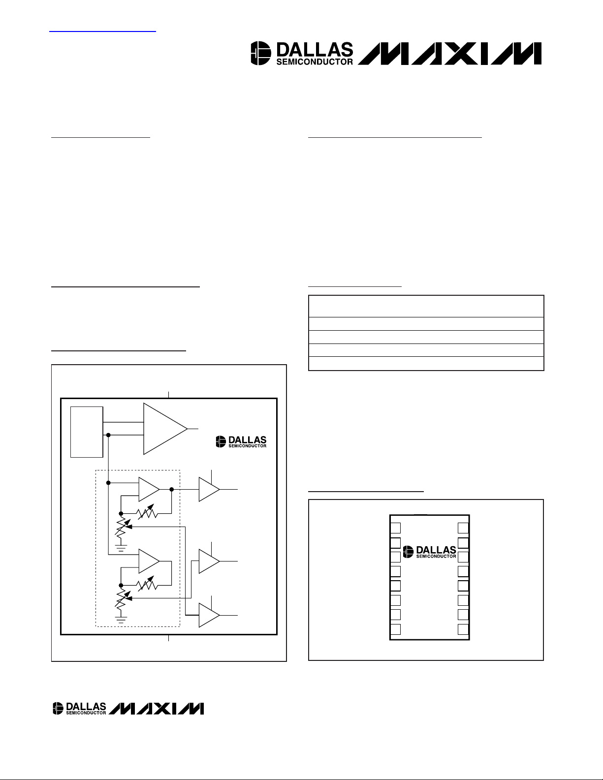
The DS2129 is a triple-output voltage regulator for
27-line, low-voltage-differential (LVD) SCSI termination
for SPI-2 and SPI-3 applications using LVD termination
networks. The device provides reference voltages and
bias currents for LVD-termination resistor pi (π) networks. With a pi network (475Ω, 121Ω, 475Ω), the
DS2129 meets the common-mode bias, differential
bias, and termination-impedance requirements of SPI-2
(Ultra2) and SPI-3 (Ultra3). The device also provides a
1.3V output for DIFFSENSE signaling, and includes protection features such as thermal shutdown and active
current limiting.
Applications
SCSI Array Backplane
SCSI Cables
Features
♦ Fully Compliant with SPI-2 and SPI-3
♦ 2.7V to 5.25V Operation
♦ Differential Fail-Safe Bias
DS2129
LVD SCSI 27-Line Regulator
______________________________________________ Maxim Integrated Products 1
16
15
14
13
12
11
10
9
1
2
3
4
5
6
7
8
N.C.
N.C.
N.C.
HS_GND
HS_GND
HS_GND
HS_GND
N.C.
N.C.
TOP VIEW
SO (150 mils)
TERMPWR
REG2
REG1
GND
HS_GND
DIFFSENSE
N.C.
DS2129
Pin Configuration
Ordering Information
Block Diagram
Rev 1; 2/06
For pricing, delivery, and ordering information, please contact Maxim/Dallas Direct! at
1-888-629-4642, or visit Maxim’s website at www.maxim-ic.com.
PART*
PINPACKAGE
TOP
MARK**
DS2129S 5 16 SO
DS2129
DS2129S+ 5 16 SO
DS2129
DS2129S/T&R 5 16 SO
DS2129
DS2129S+T&R
5 16 SO
DS2129
+Denotes lead-free package.
*All devices rated for the commercial (0°C to +70°C) tempera-
ture range.
**A “+” anywhere on the topmark denotes a lead-free package.
查询DS2065W供应商
TERMPWR
BANDGAP
(1.25V)
PTAT
REF125
THERMAL
SHUTDOWN
TS
VOLTAGE (V)
REFERENCES
REF175
REF130
REF075
GND
DS2129
TS
1.75V
REG1
TS
0.75V
REG2
TS
1.3V
DIFFSENSE
Page 2

DS2129
LVD SCSI 27-Line Regulator
2 _____________________________________________________________________
ABSOLUTE MAXIMUM RATINGS
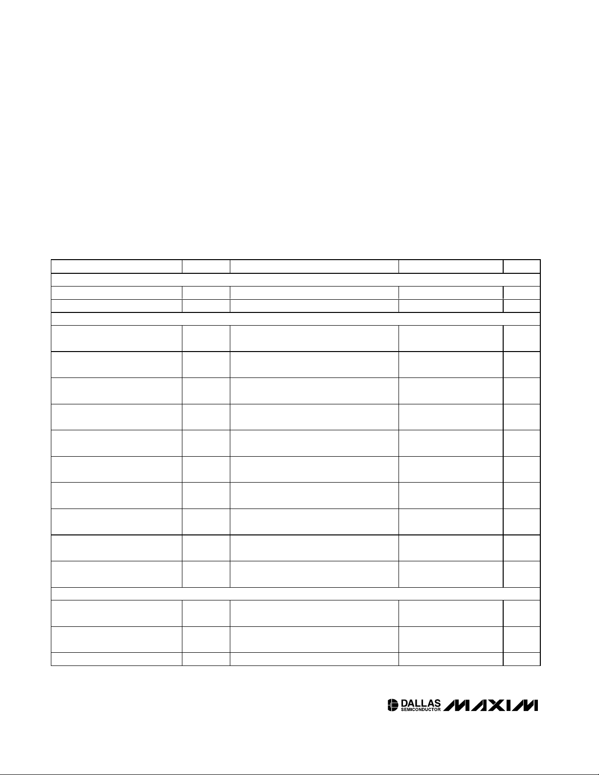
ELECTRICAL CHARACTERISTICS
(TERMPWR = 3.3V, TA= 0°C to +70°C, unless otherwise noted.) (Note 1)
Stresses beyond those listed under “Absolute Maximum Ratings” may cause permanent damage to the device. These are stress ratings only, and functional
operation of the device at these or any other conditions beyond those indicated in the operational sections of the specifications is not implied. Exposure to
absolute maximum rating conditions for extended periods may affect device reliability.
TERMPWR, DIFFSENSE, REG1, REG2 ....................-0.3V, +6.0V
REG1, REG2 Continuous Output Current.......................±200mA
Continuous Power Dissipation (T
A
= +70°C)
16-Pin SO (derate 13mW/°C above +70°C)........................1W
Operating Temperature Range...............................0°C to +70°C
Junction Temperature......................................................+150°C
Storage Temperature Range .............................-65°C to +150°C
Soldering Temperature .......................................See IPC/JEDEC
J-STD-020A Specification
PARAMETER
SYMBOL
CONDITIONS
MIN
TYP
MAX
UNITS
TERMPWR
TERMPWR Supply Current I
TERM
No load 40 mA
TERMPWR Voltage V
TERM
2.7
V
V
REF
REGULATOR
0.75V Regulator Output Voltage,
REG2
V
075
I
OUT
= ±125mA 0.7
0.8 V
0.75V Regulator Source Current,
REG2
V
OUT
= 0.25V
mA
0.75V Regulator Sink Current,
REG2
V
OUT
= 1.25V
mA
0.75V Regulator Source Current
Limit
V
OUT
= 0V
mA
0.75V Regulator Sink Current
Limit
V
OUT
= 3.3V
mA
1.75V Regulator Output Voltage,
REG1
V
175
I
OUT
= ±125mA 1.7
1.8 V
1.75V Regulator Source Current,
REG1
V
OUT
= 1.25V
mA
1.75V Regulator Sink Current,
REG1
V
OUT
= 2.25V
mA
1.75V Regulator Source Current
Limit
V
REF
= 0V
mA
1.75V Regulator Sink Current
Limit
V
REF
= 3.3V
mA
DIFFSENSE OUTPUT
DIFFSENSE Driver Output
Voltage
V
DSO
-5mA ≤ I
DIFFSENSE
≤ 50µA 1.2 1.3 1.4 V
DIFFSENSE Driver Source
Current
I
DSH
V
DIFFSENSE
= 0V -5 -15 mA
DIFFSENSE Driver Sink Current I
DSL
V
DIFFSENSE
= 2.4V 100
µA
5.25
0.75
I
SRC_075
I
SINK_075
I
SRCL_075
I
SINKL_075
I
SRC_175
I
SINK_175
I
SRCL_175
I
SINKL_175
+200
-700
1.75
+200
-700
-200
+700
-200
+700
200
Page 3

DS2129
LVD SCSI 27-Line Regulator
_____________________________________________________________________ 3
ELECTRICAL CHARACTERISTICS (continued)
(TERMPWR = 3.3V, TA= 0°C to +70°C, unless otherwise noted.) (Note 1)
Note 1: All voltages are referenced to ground.
Note 2: Guaranteed by design and not production tested.
PARAMETER
SYMBOL
CONDITIONS
MIN
TYP
MAX
UNITS
THERMAL SHUTDOWN
Thermal-Shutdown Threshold
(Note 2)
For increasing temperature
°C
Thermal-Shutdown Hysteresis
(Note 2)
10 °C
Typical Operating Circuit
TERMPWR
2.7V TO 5.25V
TERMPWR
4.7µF
DIFFSENSE
DS2129
REG1
4.7µF
+150
DIFFSENSE
R1N
475Ω
1%
121Ω
1%
REG2
4.7µF
475Ω
1%
475Ω
1%
475Ω
1%
121Ω
1%
R1P
R2N
R26P
R27N
R27P
Page 4

DS2129
LVD SCSI 27-Line Regulator
4 _____________________________________________________________________
Detailed Description
The DS2129 provides three regulated outputs. The
REG1 provides a 1.75V output, and the REG2 provides
a 0.75V output. Both regulators can sink and source
200mA of current. These regulators are current-limited
to less than 700mA. The thermal-shutdown circuit disables the output buffers should the die temperature
exceed +150°C. With a pi network of resistors (475Ω,
121Ω, 475Ω) connected to these two outputs, the
DS2129 provides common-mode bias, differential bias,
and common impedance and differential impedance,
as required in a terminator specified in SPI-2 and SPI-3
standards for a SCSI system. The third regulator provides a 1.3V output for DIFFSENSE signaling.
Chip Information
TRANSISTOR COUNT: 3778 CMOS and 80 BIPOLAR
PROCESS: BiCMOS
SUBSTRATE CONNECTED TO GROUND
Thermal Information
Thermal Resistance (junction-to-ambient):
θJA= +77°C/W
Thermal Resistance (junction-to-case):
θJC= +25°C/W
Pin Description
PIN NAME FUNCTION
1, 8, 9,
10, 15,
16
N.C.
No Connection. Do not connect pins.
2
Termination Power. Connect to SCSI
TERMPWR line and decouple with a
4.7µF ceramic capacitor.
3 REG2
Regulator 2, 0.75V Output. Decouple
with a 4.7µF ceramic capacitor.
4 GND Signal Ground
Heat-Sink Ground. Internally
connected to the mounting pad.
Should be connected to ground.
6 REG1
Regulator 1, 1.75V Output. Decouple
with a 4.7µF ceramic capacitor.
7
DIFFSENSE Output. Drives the SCSI
bus DIFFSENSE line.
TERMPWR
5, 11–14 HS_GND
DIFFSENSE
Page 5

DS2129
LVD SCSI 27-Line Regulator
Maxim cannot assume responsibility for use of any circuitry other than circuitry entirely embodied in a Maxim product. No circuit patent licenses are
implied. Maxim reserves the right to change the circuitry and specifications without notice at any time.
Maxim Integrated Products, 120 San Gabriel Drive, Sunnyvale, CA 94086 408-737-7600 _____________________ 5
© 2006 Maxim Integrated Products Printed USA is a registered trademark of Maxim Integrated Products, Inc.
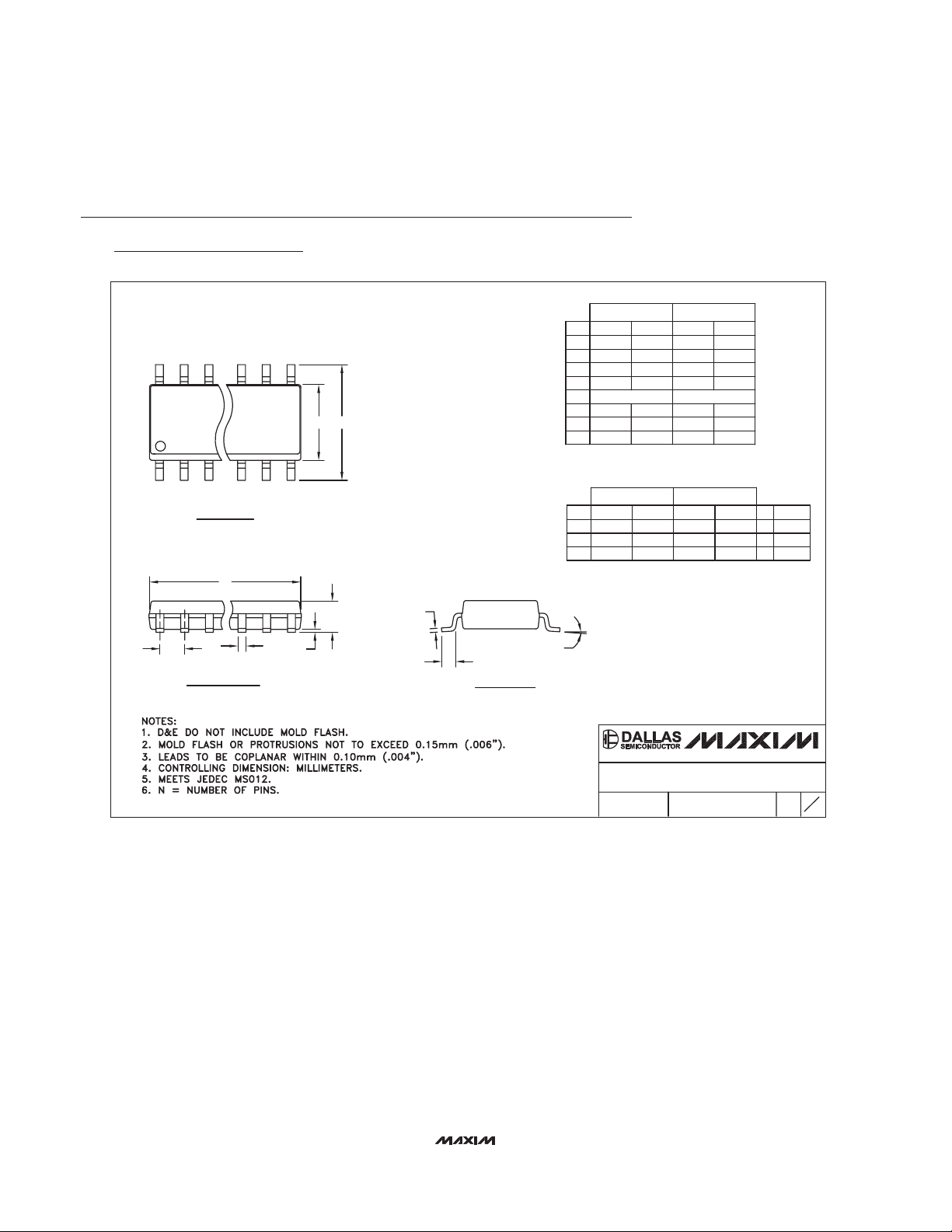
Package Information
(The package drawing(s) in this data sheet may not reflect the most current specifications. For the latest package outline information,
go to www.maxim-ic.com/packages
).
SOICN .EPS
PACKAGE OUTLINE, .150" SOIC
1
1
21-0041
B
REV.DOCUMENT CONTROL NO.APPROVAL
PROPRIETARY INFORMATION
TITLE:
TOP VIEW
FRONT VIEW
MAX
0.010
0.069
0.019
0.157
0.010
INCHES
0.150
0.007
E
C
DIM
0.014
0.004
B
A1
MIN
0.053A
0.19
3.80 4.00
0.25
MILLIMETERS
0.10
0.35
1.35
MIN
0.49
0.25
MAX
1.75
0.050
0.016L
0.40 1.27
0.3940.386D
D
MINDIM
D
INCHES
MAX
9.80 10.00
MILLIMETERS
MIN
MAX
16
AC
0.337 0.344 AB8.758.55 14
0.189 0.197 AA5.004.80 8
N MS012
N
SIDE VIEW
H 0.2440.228 5.80 6.20
e 0.050 BSC 1.27 BSC
C
HE
e
B
A1
A
D
0∞-8∞
L
1
VARIATIONS:
 Loading...