

Page 1

Maxim > App Notes > DIGITAL POTENTIOMETERS
Page 1 of 6
Keywords: DS1863
APPLICATION NOTE 4052
May 25, 2007
Quick Reference Guide to the DS1863 Memory Map
Abstract: The DS1863 burst-mode PON controller with integrated monitoring capabilities has programming options to
configure the alarms, warnings, lookup tables, and other functions. This programmability necessitates a large register
memory map. This application note provides an outline of the register map, which is convenient when programming
the device.
Memory Map of the DS1863
The DS1863 features six separate memory tables that are internally organized into eight byte rows (Figure 1).
1. The Lower Memory is addressed from 00h to 7Fh. It contains alarm and warning thresholds, flags, masks,
several control registers, password entry area (PWE), and the Table Select byte.
2. Table 01h primarily contains user EEPROM (with PW1 level access) and some alarm and warning status bytes.
3. Table 02h is a multifunction space that contains configuration registers, scaling and offset values, passwords,
interrupt registers, and miscellaneous control bytes.
4. Table 03h is strictly user EEPROM that is protected by a PW2-level password.
5. Table 04h contains a temperature-indexed lookup table (LUT) for controlling the modulation voltage. The
modulation LUT can be programmed in 2°C increments over the -40°C to +102°C range. Access to this register
is protected by a PW2-level password.
6. Table 05h contains another LUT, which allows the APC set point to change as a function of temperature to
compensate for Tracking Error (TE). This TE LUT has 36 entries that determine the APC setting in 4°C windows
between -40°C to +100°C. Access to this register is protected by a PW2-level password.
Page 2
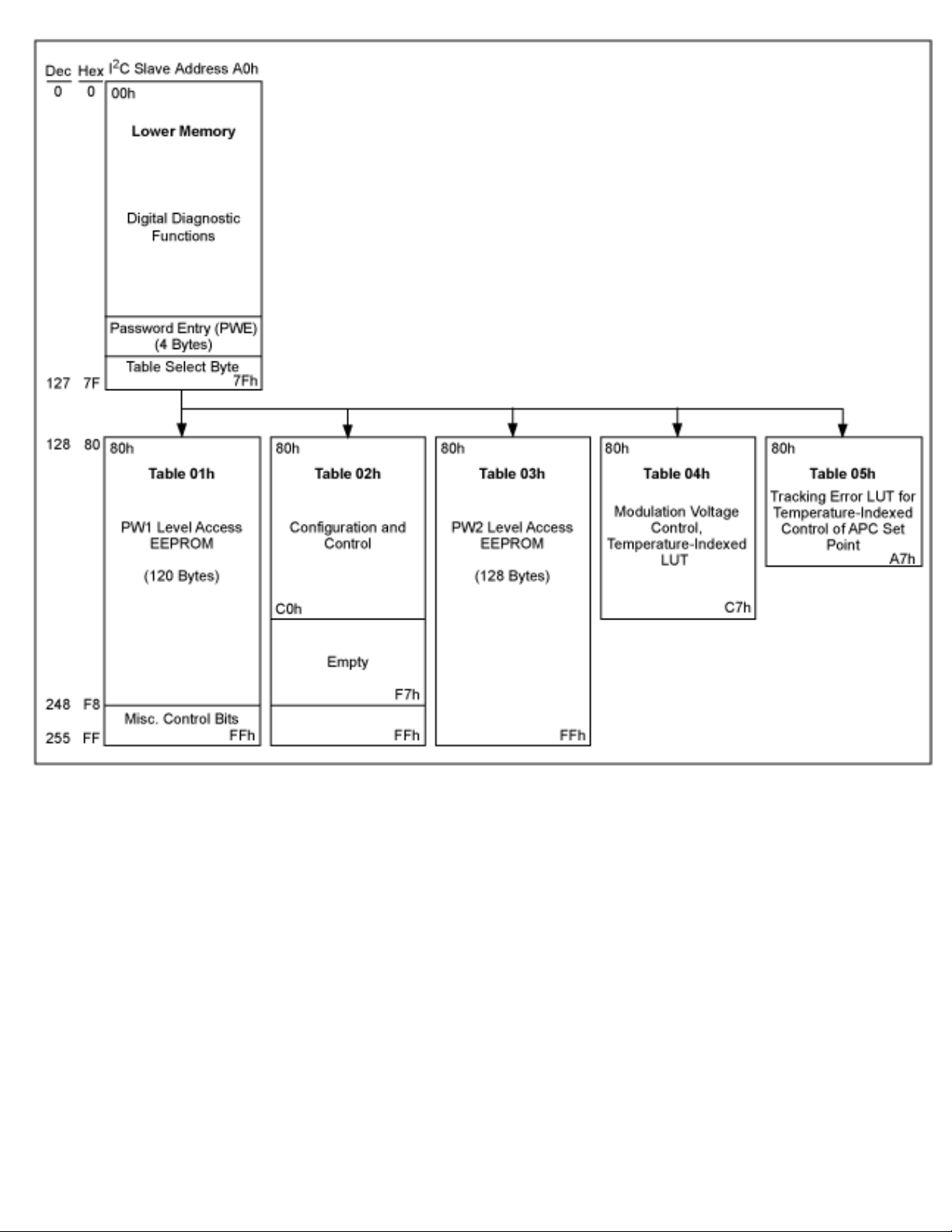
Figure 1. Structure of the memory map in the DS1863.
Page 2 of 6
Register Reference
The following tables provide an easy reference to the Lower Memory and Tables 01h and 02h. For a description of
the functionality for each bit, please refer to the corresponding register in the DS1863 data sheet. Tables 03h, 04h, and
05h are lookup tables that do not require a separate reference and, therefore, are not included here.
Note: RSVD is an acronym for RESERVED.
Page 3

Lower Memory
Page 3 of 6
Register Name Bit7 Bit0
TEMP ALARM HI
TEMP ALARM LO
TEMP WARN HI
TEMP WARN LO
VCC ALARM HI
VCC ALARM LO
VCC WARN HI
VCC WARN LO
MON1 ALARM HI
MON1 ALARM LO
MON1 WARN HI
MON1 WARN LO
MON2 ALARM HI
MON2 ALARM LO
MON2 WARN HI
MON2 WARN LO
MON3 ALARM HI
MON3 ALARM LO
MON3 WARN HI
MON3 WARN LO
00h S
01h
02h S
03h
04h S
05h
06h S
07h
08h
09h
0Ah
0Bh
0Ch
0Dh
0Eh
0Fh
10h
11h
12h
13h
14h
15h
16h
17h
18h
19h
1Ah
1Bh
1Ch
1Dh
1Eh
1Fh
20h
21h
22h
23h
24h
25h
26h
27h
6
2
-1
2
-1
2
-1
2
-1
2
15
2
7
2
15
2
7
2
15
2
7
2
15
2
7
2
15
2
7
2
15
2
7
2
15
2
7
2
15
2
7
2
15
2
7
2
15
2
7
2
15
2
7
2
15
2
7
2
15
2
7
2
15
2
7
2
15
2
7
2
15
2
7
2
-2
2
6
2
-2
2
6
2
-2
2
6
2
-2
2
14
2
6
2
14
2
6
2
14
2
6
2
14
2
6
2
14
2
6
2
14
2
6
2
14
2
6
2
14
2
6
2
14
2
6
2
14
2
6
2
14
2
6
2
14
2
6
2
14
2
6
2
14
2
6
2
14
2
6
2
14
2
6
2
5
2
-3
2
5
2
-3
2
5
2
-3
2
5
2
-3
2
13
2
5
2
13
2
5
2
13
2
5
2
13
2
5
2
13
2
5
2
13
2
5
2
13
2
5
2
13
2
5
2
13
2
5
2
13
2
5
2
13
2
5
2
13
2
5
2
13
2
5
2
13
2
5
2
13
2
5
2
13
2
5
2
4
2
-4
2
4
2
-4
2
4
2
-4
2
4
2
-4
2
12
2
4
2
12
2
4
2
12
2
4
2
12
2
4
2
12
2
4
2
12
2
4
2
12
2
4
2
12
2
4
2
12
2
4
2
12
2
4
2
12
2
4
2
12
2
4
2
12
2
4
2
12
2
4
2
12
2
4
2
12
2
4
2
3
2
-5
2
3
2
-5
2
3
2
-5
2
3
2
-5
2
11
2
3
2
11
2
3
2
11
2
3
2
11
2
3
2
11
2
3
2
11
2
3
2
11
2
3
2
11
2
3
2
11
2
3
2
11
2
3
2
11
2
3
2
11
2
3
2
11
2
3
2
11
2
3
2
11
2
3
2
11
2
3
2
2
2
-6
2
2
2
-6
2
2
2
-6
2
2
2
-6
2
10
2
2
2
10
2
2
2
10
2
2
2
10
2
2
2
10
2
2
2
10
2
2
2
10
2
2
2
10
2
2
2
10
2
2
2
10
2
2
2
10
2
2
2
10
2
2
2
10
2
2
2
10
2
2
2
10
2
2
2
10
2
2
2
1
2
-7
2
1
2
-7
2
1
2
-7
2
1
2
-7
2
9
2
1
2
9
2
1
2
9
2
1
2
9
2
1
2
9
2
1
2
9
2
1
2
9
2
1
2
9
2
1
2
9
2
1
2
9
2
1
2
9
2
1
2
9
2
1
2
9
2
1
2
9
2
1
2
9
2
1
2
9
2
1
2
SHADOWED EEPROM 28h-2Fh SEE SEE SEE SEE SEE SEE SEE SEE
0
2
-8
2
0
2
-8
2
0
2
-8
2
0
2
-8
2
8
2
0
2
8
2
0
2
8
2
0
2
8
2
0
2
8
2
0
2
8
2
0
2
8
2
0
2
8
2
0
2
8
2
0
2
8
2
0
2
8
2
0
2
8
2
0
2
8
2
0
2
8
2
0
2
8
2
0
2
8
2
0
2
Page 4

PW2 EE 30h-5Fh EE EE EE EE EE EE EE EE
Page 4 of 6
TEMP VALUE
61h
VCC VALUE
62h
63h
64h
MON1 VALUE
65h
66h
MON2 VALUE
67h
68h
MON3 VALUE
69h
STATUS 6Eh
-1
2
15
2
7
2
15
2
7
2
15
2
7
2
15
2
7
2
FETG
STATUS
UPDATE 6Fh TEMP RDY
60h S
ALARM
3
70h TEMP HI TEMP LO
6
2
-2
2
14
2
6
2
14
2
6
2
14
2
6
2
14
2
6
2
SOFT
FETG
V
RDY
CC
5
2
-3
2
13
2
5
2
13
2
5
2
13
2
5
2
13
2
5
2
RSVD
4
2
-4
2
12
2
4
2
12
2
4
2
12
2
4
2
12
2
4
2
TX-F
RESET
3
2
-5
2
11
2
3
2
11
2
3
2
11
2
3
2
11
2
3
2
SOFT
TX-D
2
2
-6
2
10
2
2
2
10
2
2
2
10
2
2
2
10
2
2
2
TX-F
STATUS
1
2
-7
2
9
2
1
2
9
2
1
2
9
2
1
2
9
2
1
2
2
2
2
2
2
2
2
2
2
2
RSVD RDYB
MON1 RDY MON2 RDY MON3 RDY RSVD RSVD RSVD
V
HI VCC LO
CC
MON1 HI MON1 LO MON2 HI MON2 LO
0
-8
8
0
8
0
8
0
8
0
ALARM
ALARM
ALARM
WARN
WARN
2
1
0
3
2
PASSWORD ENTRY
(PWE)
TABLE SELECT (TBL
SEL)
71h MON3 HI MON3 LO RSVD RSVD RSVD RSVD RSVD RSVD
72h RSVD RSVD RSVD RSVD BIAS HI RSVD TX-P HI TX-P LO
73h RSVD RSVD RSVD RSVD BIAS MAX RSVD RSVD RSVD
V
74h TEMP HI TEMP LO
HI VCC LO
CC
MON1 HI MON1 LO MON2 HI MON2 LO
75h MON3 HI MON3 LO RSVD RSVD RSVD RSVD RSVD RSVD
7Bh
7Ch
7Dh
7Eh
7Fh
31
2
23
2
15
2
7
2
7
2
30
2
22
2
14
2
6
2
6
2
29
2
21
2
13
2
5
2
5
2
28
2
20
2
12
2
4
2
4
2
27
2
19
2
11
2
3
2
3
2
26
2
18
2
10
2
2
2
2
2
Table 01h
Bit7 Bit0
PW1 EEPROM 80h-F7h EE EE EE EE EE EE EE EE
V
ALARM
ALARM
3
2
F8h TEMP HI TEMP LO
F9h MON3 HI MON3 LO RSVD RSVD RSVD RSVD RSVD RSVD
HI VCC LO
CC
MON1 HI MON1 LO MON2 HI MON2 LO
25
2
17
2
9
2
1
2
1
2
24
2
16
2
8
2
0
2
0
2
ALARM
ALARM
WARN
WARN
1
0
3
2
FAh RSVD RSVD RSVD RSVD BIAS HI RSVD TX-P HI TX-P LO
FBh RSVD RSVD RSVD RSVD BIAS MAX RSVD RSVD RSVD
V
FCh TEMP HI TEMP LO
HI VCC LO
CC
MON1 HI MON1 LO MON2 HI MON2 LO
FDh MON3 HI MON3 LO RSVD RSVD RSVD RSVD RSVD RSVD
Page 5
Page 5 of 6
Table 02h
Bit7 Bit0
MODE 80h SEEB RSVD RSVD RSVD AEN MOD-EN APC-EN BIAS-EN
T INDEX 81h
MOD DAC 82h
APC DAC 83h
84h 0 0
BIAS DAC
85h
7
2
7
2
7
2
7
2
6
2
6
2
6
2
6
2
5
2
5
2
5
2
12
2
5
2
4
2
4
2
4
2
11
2
4
2
3
2
3
2
3
2
10
2
3
2
2
2
2
2
2
2
9
2
2
2
1
2
1
2
1
2
8
2
1
2
0
2
0
2
0
2
7
2
0
2
DEVICE ID 86h 0 1 1 0 0 0 1 1
DEVICE VER 87h DEVICE VERSION
UPDATE RATE 86h 0 0 0 0 SR(3:0) SR(3:0) SR(3:0) SR(3:0)
CONFIG 89h FETG DIR TX-F EN RSVD ASEL RSVD RSVD RSVD RSVD
START-UP STEP 8Ah
12
2
MOD RANGING 8Bh RSVD RSVD RSVD RSVD RSVD
DEVICE ADDRESS 8Ch
7
2
COMP RANGING 8Dh RSVD RSVD RSVD RSVD RSVD
11
2
6
2
10
2
5
2
9
2
4
2
8
2
3
2
7
2
MOD
2
2
APC
6
2
MOD
2
1
2
APC
2
1
5
2
MOD
1
0
X
APC
0
RIGHT SHIFT
RIGHT SHIFT
V
SCALE
CC
1
0
MON1-4 SCALE
VCC OFFSET
MON1-4 OFFSET
TEMP OFFSET
PW1, PW2
FETG ENABLE
1
8Eh RSVD MON1_2 MON1_1 MON1_0 RSVD MON2_2 MON2_1 MON2_0
8Fh RSVD MON3_2 MON3_1 MON3_0 RSVD RSVD RSVD RSVD
92, 94,
96, 98,
15
2
14
2
13
2
12
2
11
2
10
2
9
2
8
2
9Ah
93, 95,
97, 99,
7
2
6
2
5
2
4
2
3
2
2
2
1
2
0
2
9Bh
A2, A4,
A6, A8,
S S
15
2
14
2
13
2
12
2
11
2
10
2
AAh
A3, A5,
A7, A9,
9
2
8
2
7
2
6
2
5
2
4
2
3
2
2
2
ABh
AEh S
AFh
B0h, B4h
B1h, B5h
B2h, B6h
B3h, B7h
1
2
31
2
23
2
15
2
7
2
B8h TEMP EN
8
2
0
2
30
2
22
2
14
2
6
2
V
EN
CC
7
2
-1
2
29
2
21
2
13
2
5
2
6
2
-2
2
28
2
20
2
12
2
4
2
5
2
-3
2
27
2
19
2
11
2
3
2
4
2
-4
2
26
2
18
2
10
2
2
2
3
2
-5
2
25
2
17
2
9
2
1
2
2
2
-6
2
24
2
16
2
8
2
0
2
MON1 EN MON2 EN MON3 EN RSVD RSVD RSVD
FETG ENABLE
TX-F ENABLE
TX-F ENABLE
HTXP BCh
LTXP BDh
HBIAS BEh
MAX IBIAS BFh
B9h TX-P HI EN TX-P LO EN BIAS HI EN BIAS MAX EN RSVD RSVD RSVD RSVD
0
V
BAh TEMP EN
1
BBh TX-P HI EN TX-P LO EN BIAS HI EN BIAS MAX EN RSVD RSVD RSVD FETG EN
0
7
2
7
2
7
2
12
2
EN
CC
6
2
6
2
6
2
11
2
MON1 EN MON2 EN MON3 EN RSVD RSVD RSVD
5
2
5
2
5
2
10
2
4
2
4
2
4
2
9
2
3
2
3
2
3
2
8
2
2
2
2
2
2
2
7
2
1
2
1
2
1
2
6
2
0
2
0
2
0
2
5
2
Page 6

MAN IBIAS
Page 6 of 6
F8h RSVD RSVD
F9h
7
2
6
2
12
2
5
2
11
2
4
2
10
2
3
2
9
2
2
2
8
2
1
2
7
2
0
2
MAN_CNTL FAh RSVD RSVD RSVD RSVD RSVD RSVD RSVD MAN_CLK
Application Note 4052: http://www.maxim-ic.com/an4052
More Information
For technical questions and support:
For samples:
http://www.maxim-ic.com/samples
Other questions and comments:
http://www.maxim-ic.com/support
http://www.maxim-ic.com/contact
Related Parts
DS1863:
QuickView -- Full (PDF) Data Sheet -- Free Samples
AN4052, AN 4052, APP4052, Appnote4052, Appnote 4052
Copyright © by Maxim Integrated Products
Additional legal notices:
http://www.maxim-ic.com/legal
 Loading...