

Page 1
DS1859
Dual, Temperature-Controlled Resistors with
Internally Calibrated Monitors
______________________________________________ Maxim Integrated Products 1
For pricing delivery, and ordering information please contact Maxim/Dallas Direct! at
1-888-629-4642, or visit Maxim’s website at www.maxim-ic.com.
General Description
The DS1859 dual, temperature-controlled, nonvolatile
(NV) variable resistors with three monitors consists of
two 50kΩ or two 20kΩ, 256-position, linear, variable
resistors; three analog monitor inputs (MON1, MON2,
MON3); and a direct-to-digital temperature sensor. The
device provides an ideal method for setting and temperature-compensating bias voltages and currents in
control applications using minimal circuitry. The variable resistor settings are stored in EEPROM memory
and can be accessed over the 2-wire serial bus.
Applications
Optical Transceivers
Optical Transponders
Instrumentation and Industrial Controls
RF Power Amps
Diagnostic Monitoring
Features
♦ SFF-8472 Compatible
♦ Five Monitored Channels (Temperature, VCC,
MON1, MON2, MON3)
♦ Three External Analog Inputs (MON1, MON2, MON3)
That Support Internal and External Calibration
♦ Scalable Dynamic Range for External Analog Inputs
♦ Internal Direct-to-Digital Temperature Sensor
♦ Alarm and Warning Flags for All Monitored
Channels
♦ Two 50kΩ or Two 20kΩ, Linear, 256-Position,
Nonvolatile Temperature-Controlled Variable
Resistors
♦ Resistor Settings Changeable Every 2°C
♦ Access to Monitoring and ID Information
Configurable with Separate Device Addresses
♦ 2-Wire Serial Interface
♦ Two Buffers with TTL/CMOS-Compatible Inputs and
Open-Drain Outputs
♦ Operates from a 3.3V or 5V Supply
♦ Operating Temperature Range of -40°C to +95°C
Ordering Information
Rev 4; 2/06
EVALUATION KIT
AVAILABLE
PART
RESISTANCE
PIN-PACKAGE
DS1859B-020 20kΩ 16 CSBGA
DS1859B-020+ 20kΩ 16 CSBGA
DS1859B-050 50kΩ 16 CSBGA
DS1859B-050+ 50kΩ 16 CSBGA
A
TOP VIEW
B
C
D
1
CSBGA (4mm x 4mm)
1.0mm PITCH
TSSOP
324
MON3
OUT1IN2
MON1
L0GND
WPEN
L1
H0SDA
OUT2
H1
V
CC
SCLIN1
MON2
DS1859
SDA
1
2
3
4
5
6
7
8
16
15
14
13
12
11
10
9
SCL
OUT1
IN1
OUT2
IN2
WPEN
GND
V
CC
H1
L1
H0
L0
MON3
MON2
MON1
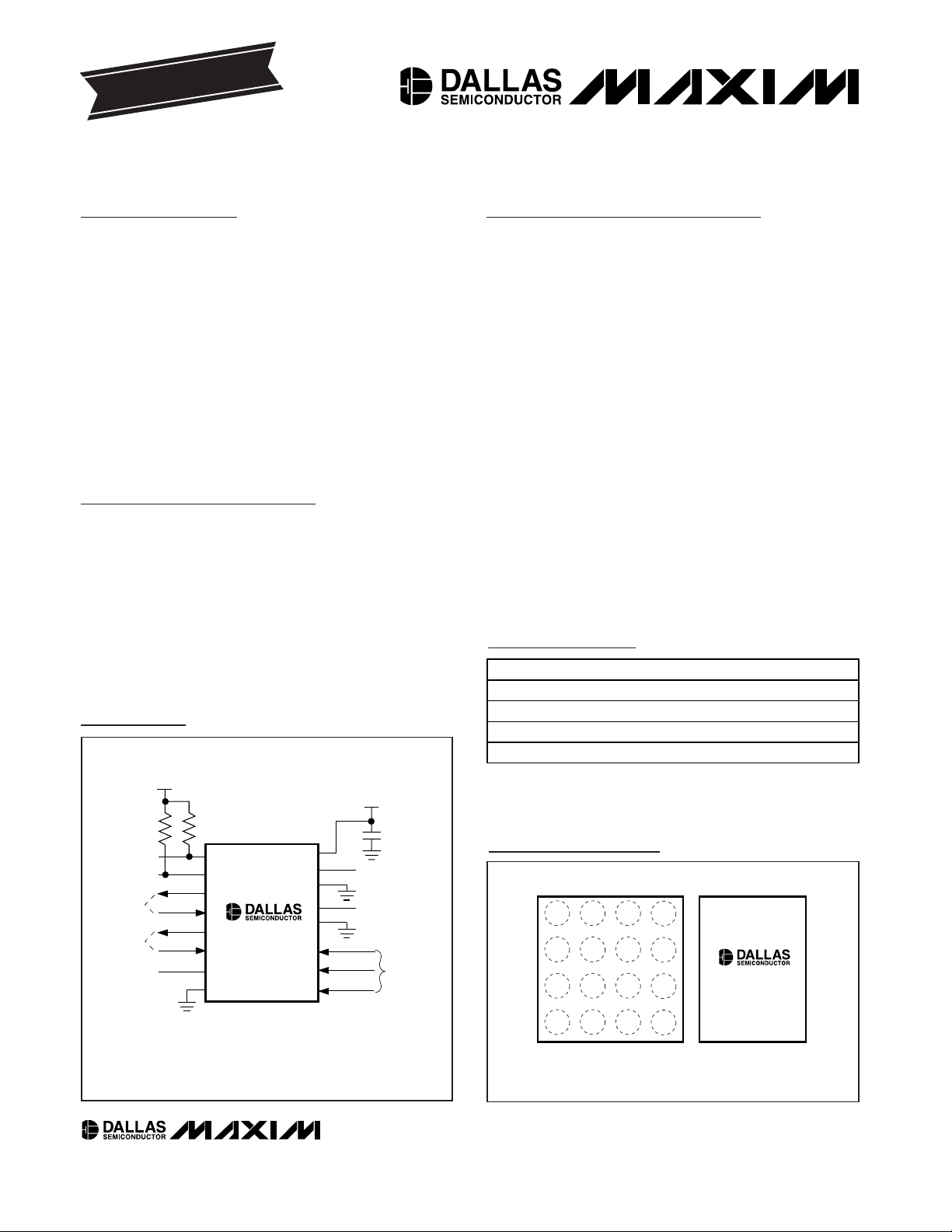
Pin Configurations
DS1859
SDA
1
2
3
4
5
6
7
8
16
0.1µF
15
14
13
12
11
10
9
SCL
OUT1
IN1
OUT2
IN2
WPEN
GND
V
CC
H1
L1
H0
L0
MON3
MON2
MON1
GROUND TO
DISABLE WRITE
PROTECT
Rx POWER*
DIAGNOSTIC
INPUTS
TO LASER
MODULATION
CONTROL
TO LASER BIAS
CONTROL
DECOUPLING
CAP
Tx POWER*
Tx BIAS*
*SATISFIES SFF-8472 COMPATIBILITY
V
CC
VCC = 3.3V
4.7kΩ4.7kΩ
Tx-FAULT
LOS
2-WIRE
INTERFACE
Typical Operating Circuit
+Denotes lead-free package.
Ordering Information continued at end of data sheet.
Page 2
DS1859
Dual, Temperature-Controlled Resistors with
Internally Calibrated Monitors
2 _____________________________________________________________________
PARAMETER
SYMBOL
CONDITIONS
MIN
TYP
MAX
UNITS
Supply Voltage V
CC
(Note 1)
5.5 V
V
IH
(Note 2)
V
V
IL
(Note 2)
V
Resistor Inputs (L0, L1, H0, H1)
V
Resistor Current I
RES
-3 +3 mA
High-Z Resistor Current I
ROFF
0.1 µA
Input logic 1
Input Logic Levels (IN1, IN2)
Input logic 0 0.9
V
ABSOLUTE MAXIMUM RATINGS
Stresses beyond those listed under “Absolute Maximum Ratings” may cause permanent damage to the device. These are stress ratings only, and functional
operation of the device at these or any other conditions beyond those indicated in the operational sections of the specifications is not implied. Exposure to
absolute maximum rating conditions for extended periods may affect device reliability.
Voltage Range on VCCRelative to Ground ...........-0.5V to +6.0V
Voltage Range on Inputs Relative
to Ground* ................................................-0.5V to V
CC
+ 0.5V
Voltage Range on Resistor Inputs Relative
to Ground* ................................................-0.5V to V
CC
+ 0.5V
Current into Resistors............................................................5mA
Operating Temperature Range ...........................-40°C to +95°C
Programming Temperature Range .........................0°C to +70°C
Storage Temperature Range .............................-55°C to +125°C
Soldering Temperature .......................................See IPC/JEDEC
J-STD-020A
RECOMMENDED DC OPERATING CONDITIONS
(TA= -40°C to +95°C, unless otherwise noted.)
PARAMETER
CONDITIONS
UNITS
Supply Current I
CC
(Note 3) 1 2 mA
Input Leakage I
IL
nA
V
OL1
3mA sink current 0 0.4
Low-Level Output Voltage
(SDA, OUT1, OUT2)
V
OL2
6mA sink current 0 0.6
V
Full-Scale Input (MON1, MON2,
MON3)
At factory setting
(Note 4)
2.5
V
Full-Scale VCC Monitor
At factory setting
(Note 5)
V
I/O Capacitance C
I/O
10 pF
WPEN Pullup R
WPEN
40 65 100 kΩ
Digital Power-On Reset POD
2.2 V
Analog Power-On Reset POA
2.6 V
DC ELECTRICAL CHARACTERISTICS
(VCC= 2.85V to 5.5V, TA= -40°C to +95°C, unless otherwise noted.)
*Not to exceed 6.0V.
Input Logic 1 (SDA, SCL, WPEN)
Input Logic 0 (SDA, SCL, WPEN)
2.85
0.7 x Vcc VCC + 0.3
-0.3 +0.3 x V
-0.3 VCC + 0.3
0.001
1.5
CC
SYMBOL
MIN TYP MAX
-200 +200
2.4875
6.5208 6.5536 6.5864
1.0
2.0
2.5125
Page 3
DS1859
Dual, Temperature-Controlled Resistors with
Internally Calibrated Monitors
_____________________________________________________________________ 3
PARAMETER
SYMBOL
CONDITIONS
MIN
TYP
MAX
UNITS
Thermometer Error T
ERR
-40°C to +95°C
°C
DIGITAL THERMOMETER
(VCC= 2.85V to 5.5V, TA= -40°C to +95°C, unless otherwise noted.)
PARAMETER
CONDITIONS
UNITS
EEPROM Writes +70°C
NONVOLATILE MEMORY CHARACTERISTICS
(VCC= 2.85V to 5.5V)
PARAMETER
CONDITIONS
Input Resolution
µV
Supply Resolution ∆V
CC
1.6 mV
Input/Supply Accuracy
(MON1, MON2, MON3, V
CC
)
A
CC
At factory setting
% FS
Update Rate for MON1, MON2,
MON3, Temp, or V
CC
t
frame
30 45 ms
Input/Supply Offset
(MON1, MON2, MON3, V
CC
)
V
OS
(Note 14) 0 5 LSB
ANALOG VOLTAGE MONITORING
(VCC= 2.85V to 5.5V, TA= -40°C to +95°C, unless otherwise noted.)
PARAMETER
SYMBOL
CONDITIONS
MIN
TYP
MAX
UNITS
Position 00h Resistance (50kΩ)T
A
= +25°C
1.0
kΩ
Position FFh Resistance (50kΩ)T
A
= +25°C 40 50 60 kΩ
Position 00h Resistance (20kΩ)T
A
= +25°C
kΩ
Position FFh Resistance (20kΩ)T
A
= +25°C 16 20 24 kΩ
Absolute Linearity (Note 6) -2 +2 LSB
Relative Linearity (Note 7) -1 +1 LSB
Temperature Coefficient (Note 8) 50
ANALOG RESISTOR CHARACTERISTICS
(VCC= 2.85V to 5.5V, TA= -40°C to +95°C, unless otherwise noted.)
SYMBOL
∆VMON 610
0.65
0.20 0.40 0.55
MIN TYP MAX UNITS
0.25 0.5
1.35
ppm/°C
(full scale)
SYMBOL
MIN TYP MAX
50,000
±3.0
Page 4
DS1859
Dual, Temperature-Controlled Resistors with
Internally Calibrated Monitors
4 _____________________________________________________________________
PARAMETER
CONDITIONS
UNITS
Fast mode (Note 9) 0 400
SCL Clock Frequency f
SCL
Standard mode (Note 9) 0 100
kHz
Fast mode (Note 9) 1.3
Bus Free Time Between STOP and
START Condition
t
BUF
Standard mode (Note 9) 4.7
µs
Fast mode (Notes 9, 10) 0.6
Hold Time (Repeated)
START Condition
Standard mode (Notes 9, 10) 4.0
µs
Fast mode (Note 9) 1.3
LOW Period of SCL Clock t
LOW
Standard mode (Note 9) 4.7
µs
Fast mode (Note 9) 0.6
HIGH Period of SCL Clock t
HIGH
Standard mode (Note 9) 4.0
µs
Fast mode (Notes 9, 11, 12) 0 0.9
Data Hold Time
Standard mode (Notes 9, 11, 12) 0
µs
Fast mode (Note 9)
Data Setup Time
Standard mode (Note 9)
ns
Fast mode (Note 9) 0.6
START Setup Time
Standard mode (Note 9) 4.7
µs
Fast mode (Note 13)
300
Rise Time of Both SDA and SCL
Signals
t
R
Standard mode (Note 13)
ns
Fast mode (Note 13)
300
Fall Time of Both SDA and SCL
Signals
t
F
Standard mode (Note 13)
300
ns
Fast mode 0.6
Setup Time for STOP Condition
Standard mode 4.0
µs
Capacitive Load for Each Bus Line
C
B
(Note 13) 400 pF
EEPROM Write Time t
W
(Note 14) 10 20 ms
AC ELECTRICAL CHARACTERISTICS
(VCC= 2.85V to 5.5V, TA= -40°C to +95°C, unless otherwise noted. See Figure 6.)
Note 1: All voltages are referenced to ground.
Note 2: I/O pins of fast-mode devices must not obstruct the SDA and SCL lines if V
CC
is switched off.
Note 3: SDA and SCL are connected to V
CC
and all other input signals are connected to well-defined logic levels.
Note 4: Full Scale is user programmable. The maximum voltage that the MON inputs read is approximately Full Scale, even if the volt-
age on the inputs is greater than Full Scale.
Note 5: This voltage defines the maximum range of the analog-to-digital converter voltage, not the maximum V
CC
voltage.
Note 6: Absolute linearity is the difference of measured value from expected value at DAC position. The expected value is a
straight line from measured minimum position to measured maximum position.
Note 7: Relative linearity is the deviation of an LSB DAC setting change vs. the expected LSB change. The expected LSB change
is the slope of the straight line from measured minimum position to measured maximum position.
Note 8: See the Typical Operating Characteristics.
Note 9: A fast-mode device can be used in a standard-mode system, but the requirement t
SU:DAT
> 250ns must then be met. This
is automatically the case if the device does not stretch the LOW period of the SCL signal. If such a device does stretch the
LOW period of the SCL signal, it must output the next data bit to the SDA line t
RMAX
+ t
SU:DAT
= 1000ns + 250ns = 1250ns
before the SCL line is released.
SYMBOL
MIN TYP MAX
t
HD:STA
t
HD:DAT
t
SU:DAT
t
SU:STA
t
SU:STO
100
250
20 + 0.1C
20 + 0.1C
20 + 0.1C
20 + 0.1C
B
B
B
B
1000
Page 5
DS1859
Dual, Temperature-Controlled Resistors with
Internally Calibrated Monitors
_____________________________________________________________________ 5
Note 10: After this period, the first clock pulse is generated.
Note 11: The maximum t
HD:DAT
only has to be met if the device does not stretch the LOW period (t
LOW
) of the SCL signal.
Note 12: A device must internally provide a hold time of at least 300ns for the SDA signal (see the V
IH MIN
of the SCL signal) to
bridge the undefined region of the falling edge of SCL.
Note 13: C
B
—total capacitance of one bus line, timing referenced to 0.9 x VCCand 0.1 x VCC.
Note 14: Guaranteed by design.
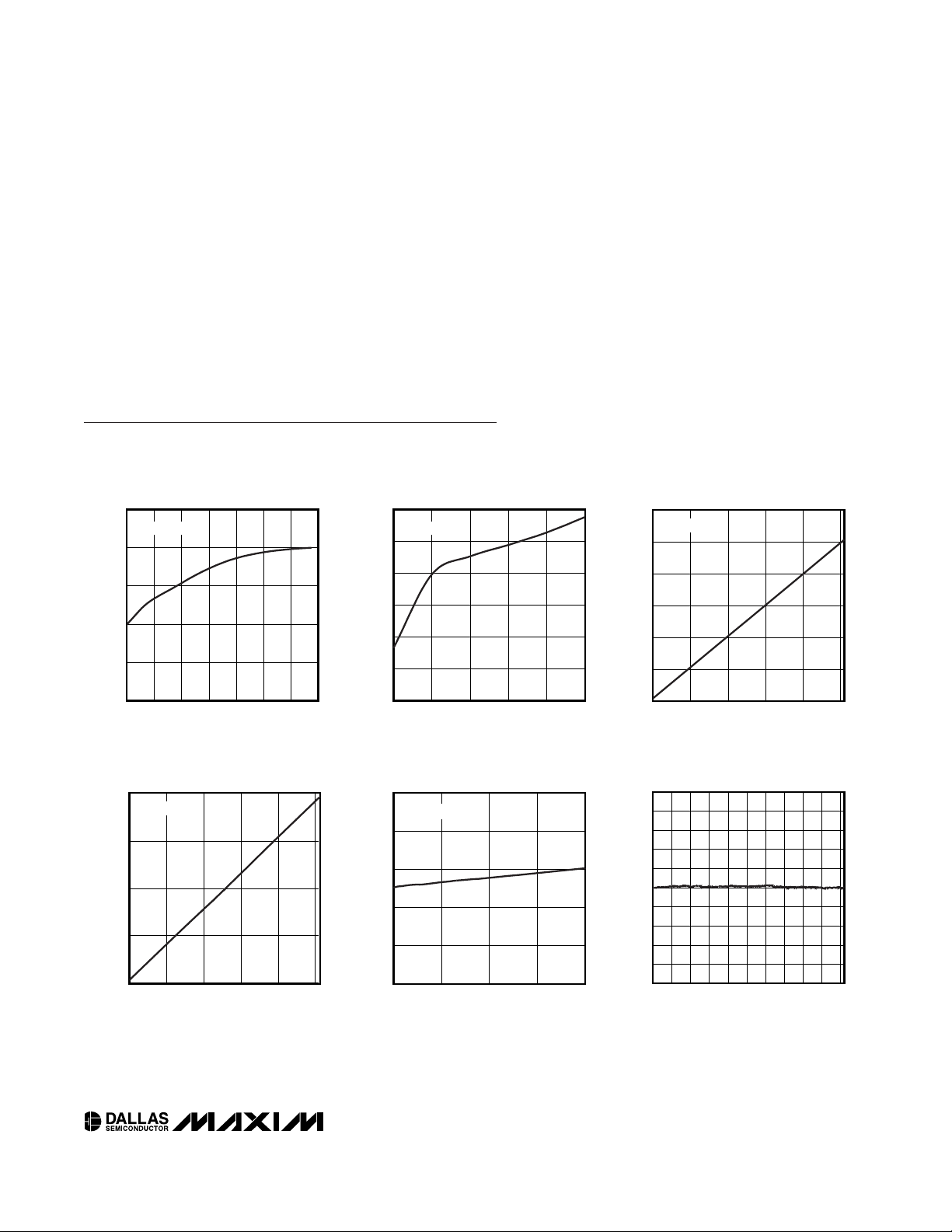
Typical Operating Characteristics
(VCC= 5.0V, TA= +25°C, for both 50kΩ and 20kΩ versions, unless otherwise noted.)
TEMPERATURE (°C)
40 60 80200-20
560
600
640
680
720
520
-40 100
SUPPLY CURRENT vs. TEMPERATURE
DS1859 toc01
SUPPLY CURRENT (µA)
SDA = SCL = V
CC
SUPPLY CURRENT vs. VOLTAGE
DS1859 toc02
VOLTAGE (V)
SUPPLY CURRENT (µA)
5.04.54.03.5
450
500
550
600
650
700
400
3.0 5.5
SDA = SCL = V
CC
RESISTANCE vs. SETTING
DS1859 toc03
SETTING (DEC)
RESISTANCE (kΩ)
20015010050
10
20
30
40
50
60
0
0 250
50kΩ VERSION
RESISTANCE vs. SETTING
DS1859 toc04
SETTING (DEC)
RESISTANCE (kΩ)
20015010050
5
10
15
20
0
0 250
20kΩ VERSION
ACTIVE SUPPLY CURRENT
vs. SCL FREQUENCY
DS1859 toc05
SCL FREQUENCY (kHz)
ACTIVE SUPPLY CURRENT (µA)
300200100
600
640
680
720
760
560
0 400
SDA = V
CC
RESISTOR 0 INL (LSB)
DS1859 toc06
SETTING (DEC)
RESISTOR 0 INL (LSB)
225200150 17550 75 100 12525
-0.8
-0.6
-0.4
-0.2
0
0.2
0.4
0.6
0.8
1.0
-1.0
0 250
Page 6
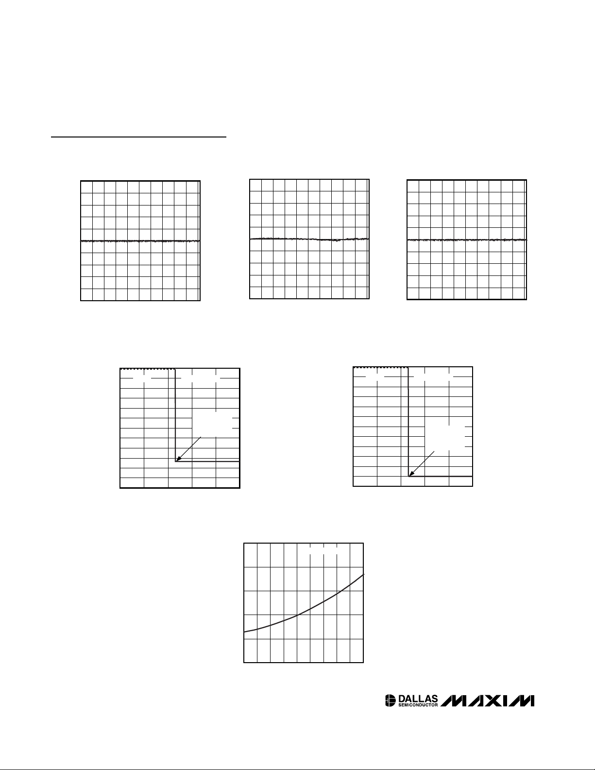
DS1859
Dual, Temperature-Controlled Resistors with
Internally Calibrated Monitors
6 _____________________________________________________________________
Typical Operating Characteristics (continued)
(VCC= 5.0V, TA= +25°C, for both 50kΩ and 20kΩ versions, unless otherwise noted.)
RESISTOR 0 DNL (LSB)
DS1859 toc07
SETTING (DEC)
RESISTOR 0 DNL (LSB)
225200150 17550 75 100 12525
-0.8
-0.6
-0.4
-0.2
0
0.2
0.4
0.6
0.8
1.0
-1.0
0 250
RESISTOR 1 INL (LSB)
DS1859 toc08
SETTING (DEC)
RESISTOR 1 INL (LSB)
225200150 17550 75 100 12525
-0.8
-0.6
-0.4
-0.2
0
0.2
0.4
0.6
0.8
1.0
-1.0
0 250
RESISTOR 1 DNL (LSB)
DS1859 toc09
SETTING (DEC)
RESISTOR 1 DNL (LSB)
225200150 17550 75 100 12525
-0.8
-0.6
-0.4
-0.2
0
0.2
0.4
0.6
0.8
1.0
-1.0
0 250
POSITION 00h RESISTANCE
vs. TEMPERATURE
DS1859 toc12
TEMPERATURE (°C)
RESISTANCE (kΩ)
20 35 50 65 805-10-25
0.96
0.97
0.98
0.99
1.00
0.95
-40 95
50kΩ VERSION
RESISTANCE
vs. POWER-UP VOLTAGE
DS1859 toc11
POWER-UP VOLTAGE (V)
RESISTANCE (kΩ)
2341
30
20
40
50
60
70
80
90
100
110
120
0
10
05
PROGRAMMED
RESISTANCE
(80h)
>1MΩ 20kΩ VERSION
RESISTANCE
vs. POWER-UP VOLTAGE
DS1859 toc10
POWER-UP VOLTAGE (V)
RESISTANCE (kΩ)
2341
30
20
40
50
60
70
80
90
100
110
120
0
10
05
PROGRAMMED
RESISTANCE
(80h)
>1MΩ 50kΩ VERSION
Page 7
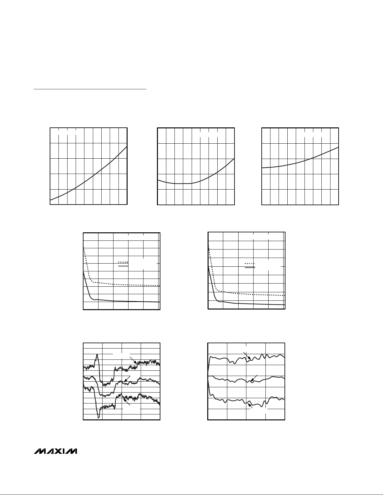
DS1859
Dual, Temperature-Controlled Resistors with
Internally Calibrated Monitors
_______________________________________________________________________________________ 7
Typical Operating Characteristics (continued)
(VCC= 5.0V, TA= +25°C, for both 50kΩ and 20kΩ versions, unless otherwise noted.)
POSITION FFh RESISTANCE
vs. TEMPERATURE
DS1859 toc14
TEMPERATURE (°C)
RESISTANCE (kΩ)
80655035205-10-25
51.20
51.40
51.60
51.80
52.00
51.00
-40 95
50kΩ VERSION
POSITION FFh RESISTANCE
vs. TEMPERATURE
DS1859 toc15
TEMPERATURE (°C)
RESISTANCE (kΩ)
80655035205-10-25
19.20
19.40
19.50
19.80
20.00
19.00
-40 95
20kΩ VERSION
TEMPERATURE COEFFICIENT vs. SETTING
DS1859 toc16
SETTING (DEC)
TEMPERATURE COEFFICIENT (ppm/°C)
20015010050
100
50
0
-50
150
200
250
300
350
400
-100
0 250
50kΩ VERSION
+25°C TO +95°C
+25°C TO -40°C
TEMPERATURE COEFFICIENT vs. SETTING
DS1859 toc17
SETTING (DEC)
TEMPERATURE COEFFICIENT (ppm/°C)
20015010050
100
0
200
300
400
500
600
700
800
-100
0 250
+25°C TO +95°C
+25°C TO -40°C
20kΩ VERSION
LSB ERROR vs. FULL-SCALE INPUT
DS1859 toc18
NORMALIZED FULL SCALE (%)
LSB ERROR
755025
-7
-6
-5
-4
-3
-2
-1
0
1
2
3
4
5
6
-8
0 100
+3 SIGMA
-3 SIGMA
MEAN
LSB ERROR vs. FULL-SCALE INPUT
DS1859 toc19
NORMALIZED FULL SCALE (%)
LSB ERROR
9.3756.2503.125
-3
-2
-1
0
1
2
3
-4
0 12.500
+3 SIGMA
-3 SIGMA
MEAN
POSITION 00h RESISTANCE
vs. TEMPERATURE
DS1859 toc13
TEMPERATURE (°C)
RESISTANCE (kΩ)
80655035205-10-25
0.34
0.35
0.36
0.37
0.38
0.33
-40 95
20kΩ VERSION
Page 8
DS1859
Dual, Temperature-Controlled Resistors with
Internally Calibrated Monitors
8 _____________________________________________________________________
Detailed Description
The user can read the registers that monitor the VCC,
MON1, MON2, MON3, and temperature analog signals.
After each signal conversion, a corresponding bit is set
that can be monitored to verify that a conversion has
occurred. The signals also have alarm and warning flags
that notify the user when the signals go above or below
the user-defined value. Interrupts can also be set for
each signal.
The position values of each resistor can be independently programmed. The user can assign a unique
value to each resistor for every 2°C increment over the
-40°C to +102°C range.
Two buffers are provided to convert logic-level inputs
into open-drain outputs. Typically, these buffers are
used to implement transmit (Tx) fault and loss-of-signal
(LOS) functionality. Additionally, OUT1 can be asserted
in the event that one or more of the monitored values
go beyond user-defined limits.
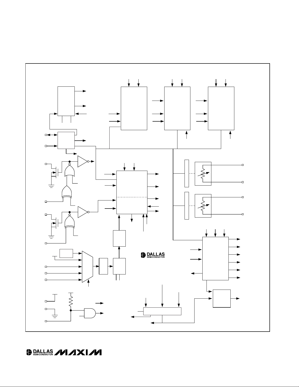
PIN
FUNCTION
1B2
2-Wire Serial Data I/O Pin. Transfers serial data to and from the device.
2A2SCL 2-Wire Serial Clock Input. Clocks data into and out of the device.
3C3
Open-Drain Buffer Output
4A1IN1 TTL/CMOS-Compatible Input to Buffer
5B1
Open-Drain Buffer Output
6C2IN2 TTL/CMOS-Compatible Input to Buffer
7C1
Write Protect Enable. The device is not write protected if WPEN is connected to ground. This pin has
an internal pullup (R
WPEN
). See Table 6.
8D1
Ground
9D3
External Analog Input
10 D4
External Analog Input
11 C4
External Analog Input
12 D2 L0
Low-End Resistor 0 Terminal. It is not required that the low-end terminals be connected to a potential
less than the high-end terminals of the corresponding resistor. Voltage applied to any of the resistor
terminals cannot exceed the power-supply voltage, V
CC
, or go below ground.
13 B3 H0
High-End Resistor 0 Terminal. It is not required that the high-end terminals be connected to a
potential greater than the low-end terminals of the corresponding resistor. Voltage applied to any of
the resistor terminals cannot exceed the power-supply voltage, V
CC
, or go below ground.
14 B4 L1 Low-End Resistor 1 Terminal
15 A4 H1 High-End Resistor 1 Terminal
16 A3 V
CC
Supply Voltage
Pin Description
BALL NAME
SDA
OUT1
OUT2
WPEN
GND
MON1
MON2
MON3
Page 9
DS1859
Dual, Temperature-Controlled Resistors with
Internally Calibrated Monitors
_____________________________________________________________________ 9
DEVICE
ADDRESS
AD (AUXILIARY DEVICE ENABLE A0h)
MD (MAIN DEVICE ENABLE)
DEVICE ADDRESS
ADDRESS
ADDRESS
ADDRESS
R/W
R/W
TxF
DATA BUS
R/W
TxF
RxL
LOS
ADEN ADFIX
SDA
SCL
IN1
OUT1
2-WIRE
INTERFACE
MINT
INV1
Tx FAULT
IN2
MON2
MON1
MON3
V
CC
GND
WPEN
OUT2
INV2
EEPROM
128 x 8 BIT
00h-7Fh
STANDARDS
PROT
AUX
AD
ADDRESS
TABLE
SELECT
R/W
EEPROM
72 x 8 BIT
80h-C7h
TABLE 02
RESISTOR 0
LOOK-UP
TABLE
PROT
MAIN
MD
EEPROM
96 x 8 BIT
00h-5Fh
LIMITS
SRAM
32 x 8 BIT
60h-7Fh
NOT PROTECTED
PROT
MAIN
MD
TEMP INDEX
ALARM FLAGS
WARNING FLAGS
MUX
CTRL
MEASUREMENT
ADDRESS
TABLE
SELECT
R/W
EEPROM
72 x 8 BIT
80h-C7h
TABLE 03
RESISTOR 1
LOOK-UP
TABLE
PROT
MAIN
MD
TEMP INDEX
R
WPEN
MONITORS LIMIT
HIGH
MONITORS LIMIT
LOW
TABLE SELECT
TEMP INDEX
MINT (BIT)
INTERNAL
TEMP
V
CC
MUX
ADC
12-BIT
INTERNAL
CALIBRATION
A/D
CTRL
V
CC
V
CC
PROT AUX
PROT MAIN
MPEN
APEN
COMPARATOR
MEASUREMENT
ALARM FLAGS
WARNING FLAGS
MONITORS LIMIT LOW
MONITORS LIMIT HIGH
COMP CTRL
INTERRUPT
MINT
TABLE 01
EEPROM
16 x 8 BIT
80h-8Fh
VENDOR
PROT
MAIN
MD R/W
DEVICE ADDRESS
ADDRESS
TABLE SELECT
MASKING (TMP, V
CC
, MON1, MON2, MON3)
ADFIX (BIT)
ADEN (BIT)
MPEN (BIT)
APEN (BIT)
INV2 (BIT)
INV1 (BIT)
RESISTOR 0
50kΩ OR 20kΩ FULL SCALE
256 POSITIONS
L0
H0
REGISTERREGISTER
RESISTOR 1
50kΩ OR 20kΩ FULL SCALE
256 POSITIONS
L1
H1
RIGHT
SHIFTING
DS1859
Figure 1. Block Diagram
Page 10

DS1859
Dual, Temperature-Controlled Resistors with
Internally Calibrated Monitors
10 ____________________________________________________________________
Monitored Signals
Each signal (VCC, MON1, MON2, MON3, and temperature) is available as a 16-bit value with 12-bit accuracy
(left-justified) over the serial bus. See Table 1 for signal
scales and Table 2 for signal format. The four LSBs
should be masked when calculating the value.
For the 20kΩ version, the 3 LSBs are internally masked
with 0s.
The signals are updated every frame rate (t
frame
) in a
round-robin fashion.
The comparison of all five signals with the high and low
user-defined values are done automatically. The corresponding flags are set to 1 within a specified time of
the occurrence of an out-of-limit condition.
Calculating Signal Values
The LSB = 100µV for VCC, and the LSB = 38.147µV for
the MON signals when using factory default settings.
To calculate VCC, convert the unsigned 16-bit value to
decimal and multiply by 100µV.
To calculate MON1, MON2, or MON3, convert the
unsigned 16-bit value to decimal and multiply by
38.147µV.
To calculate the temperature, treat the two’s complement value binary number as an unsigned binary number, then convert to decimal and divide by 256. If the
result is greater than or equal to 128, subtract 256 from
the result.
Temperature: high byte: -128°C to +127°C signed; low
byte: 1/256°C.
SIGNAL
+FS
+FS
-FS
-FS
(hex)
Temperature
-128°C 8000
V
CC
0V 0000
MON1
0V 0000
MON2
0V 0000
MON3
0V 0000
Table 1. Scales for Monitor Channels at
Factory Setting
SIGNAL FORMAT
V
CC
Unsigned
MON1 Unsigned
MON2 Unsigned
MON3 Unsigned
Temperature Two’s complement
Table 2. Signal Comparison
TEMPERATURE
(°C)
CORRESPONDING LOOK-UP
TABLE ADDRESS
<-40 80h
-40 80h
-38 81h
-36 82h
-34 83h
——
+98 C5h
+100 C6h
+102 C7h
>+102 C7h
Table 3. Look-up Table Address for
Corresponding Temperature Values
2
8
2
0
Monitor/VCCBit Weights
Temperature Bit Weights
Monitor Conversion Example
VCCConversion Examples
Temperature Conversion Examples
SIGNAL
127.984°C 7FFC
6.5528V FFF8
2.4997V FFF8
2.4997V FFF8
2.4997V FFF8
(hex)
SIGNAL
MSB (BIN) LSB (BIN) VOLTAGE (V)
11000000 00000000 1.875
10000000 10000000 1.255
S262
-1
2
-2
2
5
4
2
-3
2
-4
2
3
2
-5
2
2
2
-6
2
1
2
-7
2
0
2
-8
2
MSB 2
LSB 2
15214213212211210
7
MSB (BIN) LSB (BIN) VOLTAGE (V)
10000000 10000000 3.29
11000000 11111000 4.94
6
2
5
2
9
2
4
3
2
2
2
2
1
2
MSB (BIN) LSB (BIN) TEMPERATURE (°C)
01000000 00000000 64
01000000 00001111 64.059
01011111 00000000 95
11110110 00000000 -10
11011000 00000000 -40
Page 11

DS1859
Dual, Temperature-Controlled Resistors with
Internally Calibrated Monitors
____________________________________________________________________ 11
Variable Resistors
The value of each variable resistor is determined by
a temperature-addressed look-up table, which can
assign a unique value (00h to FFh) to each resistor for
every 2°C increment over the -40°C to +102°C range
(see Table 3). See the Temperature Conversion section
for more information.
The variable resistors can also be used in manual
mode. If the TEN bit equals 0, the resistors are in manual mode and the temperature indexing is disabled. The
user sets the resistors in manual mode by writing to
addresses 82h and 83h in Table 01 to control resistors
0 and 1, respectively.
Memory Description
Main and auxiliary memories can be accessed by two
separate device addresses. The Main Device address
is A2h (or value in Table 01 byte 8Ch, when ADFIX = 1)
and the Auxiliary Device address is A0h. A user option
is provided to respond to one or two device addresses.
This feature can be used to save component count in
SFF applications (Main Device address can be used)
or other applications where both GBIC (Auxiliary
Device address can be used) and monitoring functions
are implemented and two device addresses are needed. The memory blocks are enabled with the corresponding device address. Memory space from 80h and
ADEN
(ADDRESS
ENABLE)
NO. OF SEPARATE
DEVICE
ADDRESSES
ADDITIONAL
INFORMATION
02See Figure 2
1
See Figure 3
Table 4. ADEN Address Configuration
ADEN ADFIX
AUXILIARY
MAIN ADDRESS
00A0h A2h
01A0h
EEPROM
(Table 01, 8Ch)
10N/A A2h
11N/A
EEPROM
(Table 01, 8Ch)
Table 5. ADEN and ADFIX Bits
MAIN
DEVICE
MON LOOK-UP
TABLE CONTROL
R0 LOOK-UP
TABLE
AUXILIARY
DEVICE
0
DEC
0
95
96
127
128
143
199
MEMORY PARTITION WITH ADEN BIT = 0
EN
EN
EN
5Fh
60h
EN
SEL
EN
SEL
7Fh 7Fh
80h
80h
C7h
F0h
FFh
RESERVED
8Fh
TABLE SELECT
MAIN DEVICE ENABLE
AUXILIARY DEVICE ENABLE
DECODER
0
F0h
FFh
RESERVED
R1 LOOK-UP
TABLE
EN
SEL
80h
C7h
TABLE 03TABLE 02TABLE 01
Figure 2. Memory Organization, ADEN = 0
1 (Main Device only)
ADDRESS
Page 12

DS1859
Dual, Temperature-Controlled Resistors with
Internally Calibrated Monitors
12 ____________________________________________________________________
above is accessible only through the Main Device
address. This memory is organized as three tables. The
desired table can be selected by the contents of memory location 7Fh, Main Device. The Auxiliary Device
address has no access to the tables, but the Auxiliary
Device address can be mapped into the Main Device’s
memory space as a fourth table. Device addresses are
programmable with two control bits in EEPROM.
ADEN configures memory access to respond to different device addresses (see Tables 4 and 5).
The default device address for EEPROM-generated
addresses is A2h.
If the ADEN bit is 1, additional 128 bytes of EEPROM
are accessible through the Main Device, selected as
Table 00 (see Figure 3). In this configuration, the
Auxiliary Device is not accessible. APEN controls the
protection of Table 00 regardless of ADEN’s setting.
ADFIX (address fixed) determines whether the Main
Device address is determined by an EEPROM byte
(Table 01, byte 8Ch, when ADFIX = 1). There can be
up to 128 devices sharing a common 2-wire bus, with
each device having its own unique device address.
WPEN
MPEN PROTECT MAIN
0X No
X0 No
11 Yes
Table 6. Main Device
APEN
WPEN PROTECT AUXILIARY
0
XNo
1
X Yes
Table 7. Auxiliary Device
MAIN
DEVICE
MON LOOK-UP
TABLE CONTROL
R0 LOOK-UP
TABLE
AUXILIARY
DEVICE
80h
DEC
0
95
96
127
128
143
199
255
EN
EN
EN
5Fh
60h
EN
SEL
EN
SEL
FFh
7Fh
80h
80h
C7h
F0h
FFh
RESERVED
8Fh
TABLE SELECT
TABLE 00
MAIN DEVICE ENABLE
DECODER
0
F0h
FFh
RESERVED
R1 LOOK-UP
TABLE
EN
SEL
80h
C7h
TABLE 03TABLE 02TABLE 01
MEMORY PARTITION WITH ADEN BIT = 1
Figure 3. Memory Organization, ADEN = 1
Page 13

DS1859
Dual, Temperature-Controlled Resistors with
Internally Calibrated Monitors
____________________________________________________________________ 13
MEMORY LOCATION
(hex)
EEPROM/SRAM
R/W
DEFAULT SETTING
(hex)
NAME OF LOCATION FUNCTION
00 to 7F EEPROM
00 Standards Data —
Auxiliary Device
MEMORY
LOCATION
(hex)
EEPROM/
SRAM
DEFAULT
(hex)
FUNCTION
00 to 01 EEPROM
00
Contains upper limit settings for temperature.
If the limit is violated, an alarm flag in Main
Device byte 70h is set.
02 to 03 EEPROM
00
Contains lower limit settings for temperature. If
the limit is violated, an alarm flag in Main
Device byte 70h is set.
04 to 05 EEPROM
00
Contains upper limit settings for temperature.
If the limit is violated, a warning flag in Main
Device byte 74h is set.
06 to 07 EEPROM
00
Contains lower limit settings for temperature. If
the limit is violated, a warning flag in Main
Device byte 74h is set.
08 to 09 EEPROM
00
Contains upper limit settings for VCC. If the
limit is violated, an alarm flag in Main Device
byte 70h is set.
0A to 0B EEPROM
00
Contains lower limit settings for VCC. If the
limit is violated, an alarm flag in Main Device
byte 70h is set.
0C to 0D EEPROM
00
Contains upper limit settings for VCC. If the
limit is violated, a warning flag in Main Device
byte 74h is set.
0E to 0F EEPROM
00
Contains lower limit settings for VCC. If the
limit is violated, a warning flag in Main Device
byte 74h is set.
10 to 11 EEPROM
00
Contains upper limit settings for MON1. If the
limit is violated, an alarm flag in Main Device
byte 70h is set.
Main Device
Note: SRAM defaults are power-on defaults. EEPROM defaults are factory defaults.
Register Map
A description of the registers is below. The registers
are read only (R) or read/write (R/W). The R/W registers
are writable only if write protect has not been asserted
(see the Memory Description section).
Bytes designated as "Reserved" have been set aside
for added functionality in future revisions of this device.
R/W
R/W
R/W
R/W
R/W
R/W
R/W
R/W
R/W
R/W
R/W
SETTING
NAME OF LOCATION
TMPlimhi (MSB to LSB)
TMPlimlo (MSB to LSB)
TMPwrnhi (MSB to LSB)
TMPwrnlo (MSB to LSB)
VCClimhi (MSB to LSB)
VCClimlo (MSB to LSB)
VCCwrnhi (MSB to LSB)
VCCwrnlo (MSB to LSB)
MON1limhi (MSB to LSB)
Page 14

DS1859
Dual, Temperature-Controlled Resistors with
Internally Calibrated Monitors
14 ____________________________________________________________________
MEMORY
LOCATION
(hex)
EEPROM/
SRAM
R/W
DEFAULT
(hex)
NAME OF LOCATION
FUNCTION
12 to 13 EEPROM
00
Contains lower limit settings for MON1. If the
limit is violated, an alarm flag in Main Device
byte 70h is set.
14 to 15 EEPROM
00
MON1wrnhi
(MSB to LSB)
Contains upper limit settings for MON1. If the
limit is violated, a warning flag in Main Device
byte 74h is set.
16 to 17 EEPROM
00
MON1wrnlo
(MSB to LSB)
Contains lower limit settings for MON1. If the
limit is violated, a warning flag in Main Device
byte 74h is set.
18 to 19 EEPROM
00
Contains upper limit settings for MON2. If the
limit is violated, an alarm flag in Main Device
byte 70h is set.
1A to 1B EEPROM
00
Contains lower limit settings for MON2. If the
limit is violated, an alarm flag in Main Device
byte 70h is set.
1C to 1D EEPROM
00
MON2wrnhi
(MSB to LSB)
Contains upper limit settings for MON2. If the
limit is violated, a warning flag in Main Device
byte 74h is set.
1E to 1F EEPROM
00
MON2wrnlo
(MSB to LSB)
Contains lower limit settings for MON2. If the
limit is violated, a warning flag in Main Device
byte 74h is set.
20 to 21 EEPROM
00
Contains upper limit settings for MON3. If the
limit is violated, an alarm flag in Main Device
byte 71h is set.
22 to 23 EEPROM
00
Contains lower limit settings for MON3. If the
limit is violated, an alarm flag in Main Device
byte 71h is set.
24 to 25 EEPROM
00
MON3wrnhi
(MSB to LSB)
Contains upper limit settings for MON3. If the
limit is violated, a warning flag in Main Device
byte 75h is set.
26 to 27 EEPROM
00
MON3wrnlo
(MSB to LSB)
Contains lower limit settings for MON3. If the
limit is violated, a warning flag in Main Device
byte 75h is set.
28 to 37 EEPROM — — Reserved —
38 to 5F EEPROM
— Memory —
60 to 61 SRAM R —
Measured TMP
(MSB to LSB)
Digitized measured value for temperature.
See Table 1.
62 to 63 SRAM R —
Measured V
CC
(MSB to LSB)
Digitized measured value for V
CC
.
See Table 1.
64 to 65 SRAM R —
Measured MON1
(MSB to LSB)
Digitized measured value for MON1.
See Table 1.
66 to 67 SRAM R —
Measured MON2
(MSB to LSB)
Digitized measured value for MON2.
See Table 1.
Main Device (continued)
SETTING
R/W
MON1limlo (MSB to LSB)
R/W
R/W
R/W
R/W
R/W
R/W
R/W
R/W
R/W
R/W
R/W
MON2limhi (MSB to LSB)
MON2limlo (MSB to LSB)
MON3limhi (MSB to LSB)
MON3limlo (MSB to LSB)
Page 15

DS1859
Dual, Temperature-Controlled Resistors with
Internally Calibrated Monitors
____________________________________________________________________ 15
MEMORY
LOCATION
(hex)
EEPROM/
SRAM
DEFAULT
(hex)
FUNCTION
68 to 69 SRAM R —
Measured MON3
(MSB to LSB)
Digitized measured value for MON3.
See Table 1.
6A to 6D SRAM — — Reserved —
6E SRAM — — Logic states —
Bit 7 — R X HIZSTA
Resistor status bit. A high indicates that both
resistors are in high-impedance mode. A low
indicates that both resistors are operating
normally.
6—
0 HIZCO
Resistor control bit. Setting this bit high
causes both resistors to go into a highimpedance state.
5——X X —
4——X X —
3——X X —
2—RX TXF
This status bit is high when OUT1 is high,
assuming there is an external pullup resistor
on OUT1.
1—RX RXL
This status bit is high when OUT2 is high,
assuming there is an external pullup resistor
on OUT2.
0—RX RDYB
This status bit goes high when V
CC
has fallen
below the POA level.
6F SRAM — — Conversion updates —
Bit 7 —
0 TAU
This bit goes high after a temperature and
address update has occurred for the
corresponding measurement in bytes 60h to
61h. This bit can be written to a 0 by the user
and monitored to verify that a conversion has
occurred.
6—
0V
CC
U
This bit goes high after a V
CC
update has
occurred for the corresponding measurement
in bytes 62h to 63h. This bit can be written to
a 0 by the user and monitored to verify that a
conversion has occurred.
5—
0 MON1U
This bit goes high after a MON1 update has
occurred for the corresponding measurement
in bytes 64h to 65h. This bit can be written to
a 0 by the user and monitored to verify that a
conversion has occurred.
Main Device (continued)
R/W
R/W
R/W
SETTING
NAME OF LOCATION
R/W
R/W
Page 16

DS1859
Dual, Temperature-Controlled Resistors with
Internally Calibrated Monitors
16 ____________________________________________________________________
MEMORY
LOCATION
(hex)
EEPROM/
SRAM
R/W
DEFAULT
(hex)
NAME OF LOCATION
FUNCTION
4—
0 MON2U
This bit goes high after a MON2 update has
occurred for the corresponding measurement
in bytes 66h to 67h. This bit can be written to
a 0 by the user and monitored to verify that a
conversion has occurred.
3——0 MON3U
This bit goes high after a MON3 update has
occurred for the corresponding measurement
in bytes 68h to 69h. This bit can be written to
a 0 by the user and monitored to verify that a
conversion has occurred.
2——0 — —
1——0 — —
0——0 — —
70 SRAM R Alarm flags —
Bit 7 — — — TMPhi
This alarm flag goes high when the upper limit
of the temperature setting is violated.
6——— TMPlo
This alarm flag goes high when the lower limit
of the temperature setting is violated.
5——— V
CC
hi
This alarm flag goes high when the upper limit
of the V
CC
setting is violated.
4——— V
CC
lo
This alarm flag goes high when the lower limit
of the V
CC
setting is violated.
3——— MON1hi
This alarm flag goes high when the upper limit
of the MON1 setting is violated.
2——— MON1lo
This alarm flag goes high when the lower limit
of the MON1 setting is violated.
1——— MON2hi
This alarm flag goes high when the upper limit
of the MON2 setting is violated.
0——— MON2lo
This alarm flag goes high when the lower limit
of the MON2 setting is violated.
71 SRAM R — Alarm flags —
Bit 7 — — — MON3hi
This alarm flag goes high when the upper limit
of the MON3 setting is violated.
6——— MON3lo
This alarm flag goes high when the lower limit
of the MON3 setting is violated.
5——— X —
4——— X —
Main Device (continued)
SETTING
R/W
Page 17

DS1859
Dual, Temperature-Controlled Resistors with
Internally Calibrated Monitors
____________________________________________________________________ 17
MEMORY
LOCATION
(hex)
EEPROM/
SRAM
R/W
DEFAULT
(hex)
NAME OF LOCATION
FUNCTION
3——— X —
2——— X —
1——— X —
0——— MINT
A mask of all flags located in Table 01 byte
88h determines the value of MINT. MINT is
maskable to 0 if no interrupt is desired by
setting Table 01 byte 88h to 0.
72 to 73 SRAM — — Reserved —
74 SRAM R — Warning flags —
Bit 7 — — — TMPhi
This warning flag goes high when the upper
limit of the temperature setting is violated.
6——— TMPlo
This warning flag goes high when the lower
limit of the temperature setting is violated.
5——— V
CC
hi
This warning flag goes high when the upper
limit of the V
CC
setting is violated.
4——— V
CC
lo
This warning flag goes high when the lower
limit of the V
CC
setting is violated.
3——— MON1hi
This warning flag goes high when the upper
limit of the MON1 setting is violated.
2——— MON1lo
This warning flag goes high when the lower
limit of the MON1 setting is violated.
1——— MON2hi
This warning flag goes high when the upper
limit of the MON2 setting is violated.
0——— MON2lo
This warning flag goes high when the lower
limit of the MON2 setting is violated.
Main Device (continued)
SETTING
Page 18

DS1859
Dual, Temperature-Controlled Resistors with
Internally Calibrated Monitors
18 ____________________________________________________________________
MEMORY
LOCATION
(hex)
EEPROM/
SRAM
R/W
DEFAULT
(hex)
NAME OF LOCATION
FUNCTION
75 SRAM R — Warning Flags —
Bit 7 — — 0 MON3hi
This warning flag goes high when the upper
limit of the MON3 setting is violated.
6——0 MON3lo
This warning flag goes high when the lower
limit of the MON3 setting is violated.
5——0 X —
4——0 X —
3——0 X —
2——0 X —
1——0 X —
76 to 7E SRAM — — Reserved —
7F SRAM
— Table select —
Bit 7 — — 0 X —
6——0 X —
5——0 X —
4——0 X —
3——0 X —
2——0 X —
1——0
0——0
Table select bits
Set bits = 00 to select Table 00, set bits = 01
to select Table 01, set bits = 10 to select
Table 02, set bits = 11 to select Table 03.
Main Device (continued)
SETTING
R/W
Page 19

DS1859
Dual, Temperature-Controlled Resistors with
Internally Calibrated Monitors
____________________________________________________________________ 19
MEMORY
LOCATION
(hex)
EEPROM/
SRAM
R/W
DEFAULT
SETTING
(hex)
NAME OF
LOCATION
FUNCTION
80 SRAM R/W Mode —
Bit 7 — — 0 X —
6——0 X —
5——0 X —
4——0 X —
3——0 X —
2——0 X —
1——1 TEN
If TEN = 0, the resistors can be controlled manually. The
user sets the resistor in manual mode by writing to
addresses 82h and 83h in Table 01 to control resistors 0
and 1, respectively.
0——1 AEN
AEN = 0 is a test mode setting and provides manual
control of the temperature index (Table 01, address 81h).
81 SRAM R —
Temperature
index
This byte is the temperature-calculated index used to
select the address of resistor settings in the look-up
tables (Tables 02 and 03, addresses 80h through C7h).
82 SRAM R/W FF Resistor 0 Resistor 0 position values from 00h to FFh.
83 SRAM R/W FF Resistor 1 Resistor 1 position values from 00h to FFh.
84 to 87 SRAM — — Reserved —
88
R/W
This byte configures a maskable interrupt, determining
which event asserts a buffer 1 output (MINT set to 1, see
register 89h in Table 01). If any combination of
temperature, V
CC
, MON1, MON2, or MON3 is desired to
generate an interrupt, the corresponding bits are set to 1.
If interrupt generation is not desired, set all bits to 0.
Bit 7 — — 1 TMP —
6——1 V
CC
—
5——1 MON1 —
4——1 MON2 —
3——1 MON3 —
2——0 X —
1——0 X —
0——0 X —
89
R/W Configuration —
Bit 7 — — 0 X —
6——0 X
Table 01h
EEPROM
EEPROM
Interrupt enable
Page 20

DS1859
Dual, Temperature-Controlled Resistors with
Internally Calibrated Monitors
20 ____________________________________________________________________
MEMORY
LOCATION
(hex)
EEPROM/
SRAM
R/W
DEFAULT
SETTING
(hex)
NAME OF
LOCATION
FUNCTION
5——0 ADEN
Controls if the device responds to one or two device
addresses (see the Memory Description section and
Table 5).
4——0 ADFIX
Controls the means by which Main and Auxiliary Device
addresses are set (see the Memory Description section
and Table 5).
3——0 APEN
Controls auxiliary write protect. See the Memory
Description section.
2——0 MPEN
Controls main write protect. See the Memory Description
section.
1——0 INV1
Configures buffer 1 with OUT1 = MINT +
(INV1 [XOR] IN1).
0——0 INV2 Configures buffer 2 with OUT2 = INV2 [XOR] IN2.
8A to 8B
—— Reserved
8C
R/W A2
Contains Main Device address if the bit ADFIX = 1. If
ADFIX = 0, then address A2h is used.
8D
—— Reserved —
8E
R/W
Contains bits used to perform right shift operations on the
A/D output converter. See the Right Shift A/D Conversion
Result section.
7——0 —
6——0 MON1
2
Right Shift Control MSB
5——0 MON1
1
4——0 MON1
0
Right Shift Control LSB
3——0 —
2——0 MON2
2
Right Shift Control MSB
1——0 MON2
1
0——0 MON2
0
Right Shift Control LSB
8F
R/W
Contains bits used to perform right shift operations on the
A/D output converter. See the Right Shift A/D Conversion
Result section.
7——0 —
6——0 MON3
2
Right Shift Control MSB
5——0 MON3
1
4——0 MON3
0
Right Shift Control LSB
3——0 —
2——0 —
1——0 —
0——0 —
Table 01h (continued)
EEPROM
EEPROM
EEPROM
EEPROM
EEPROM
Device address
Page 21

DS1859
Dual, Temperature-Controlled Resistors with
Internally Calibrated Monitors
____________________________________________________________________ 21
MEMORY
LOCATION
(hex)
EEPROM/
SRAM
R/W
DEFAULT
SETTING
(hex)
NAME OF
LOCATION
FUNCTION
90 to 91
—0 Reserved
92 to 93
R/W Gain Cal V
CC
Gain registers for internal calibration. See the Internal
Calibration section.
94 to 95
R/W
96 to 97
R/W
98 to 99
R/W
9A to 9F
— Reserved
A0 to A1
— Reserved
A2 to A3
R/W
Offset registers for internal calibration.
See the Internal Calibration section.
A4 to A5
R/W
A6 to A7
R/W
A8 to A9
R/W
AA to AD
— Reserved
AE to AF
R/W
Factory
Offset calibration for temperature calibrated at factory.
Table 01h (continued)
MEMORY
LOCATION
(hex)
EEPROM/
SRAM
R/W
DEFAULT
SETTING
(hex)
NAME OF LOCATION FUNCTION
80 to C7
R/W FF Resistor 0 Temp LUT Look-up table for Resistor 0.
F0 to F7
—— Reserved —
F8 to FF
R
Factory
Resistor 0 Cal Constants
Calibration constants for Resistor 0.
(See Table 8)
Table 02h
MEMORY
LOCATION
(hex)
EEPROM/
SRAM
R/W
DEFAULT
SETTING
(hex)
NAME OF LOCATION FUNCTION
80 to C7
R/W FF Resistor 1 Temp LUT Look-up table for Resistor 1.
F0 to F7
—— Reserved —
F8 to FF
R
Factory
Resistor 1 Cal Constants
Calibration constants for Resistor 1.
(See Table 8)
Table 03h
EEPROM
EEPROM
EEPROM
EEPROM
EEPROM
EEPROM
EEPROM
EEPROM
EEPROM
EEPROM
EEPROM
EEPROM
EEPROM
EEPROM
EEPROM
Programmed
Gain Cal Mon1
Gain Cal Mon2
Gain Cal Mon3
Offset Cal V
Offset Cal Mon1
Offset Cal Mon2
Offset Cal Mon3
Offset Cal Tmp
CC
EEPROM
EEPROM
EEPROM
EEPROM
Programmed
Programmed
Page 22

DS1859
Dual, Temperature-Controlled Resistors with
Internally Calibrated Monitors
22 ____________________________________________________________________
Programming the Look-up Table (LUT)
The following equation can be used to determine which
resistor position setting, 00h to FFh, should be written in
the LUT to achieve a given resistance at a specific temperature.
α = 3.852357 for the 20kΩ resistor
α = 4.5680475 for the 50kΩ resistor
R = the resistance desired at the output terminal
C = temperature in degrees Celsius
u, v, w, x
1
, x0, y, and z are calculated values found in the
corresponding look-up tables. The variable x from the
equation above is separated into x1(the MSB of x) and x
0
(the LSB of x). Their addresses and LSB values are given
below. Resistor 0 variables are found in Table 1, and
Resistor 1 variables are found in Table 2.
When shipped from the factory, all other memory locations in the LUTs are programmed to FFh.
Table 8. Calibration Constants
Internal Calibration
The DS1859 has two methods for scaling an analog
input to a digital result. The two methods are gain and
offset. Each of the inputs (V
CC
, MON1, MON2, and
MON3) has a unique register for the gain and the offset
found in Table 01h, 92h to 99h, and A2h to A9h.
To scale the gain and offset of the converter for a specific input, you must first know the relationship between
the analog input and the expected digital result. The
input that would produce a digital result of all zeros is
the null value (normally this input is GND). The input
that would produce a digital result of all ones is the fullscale (FS) value. The FS value is also found by multiplying an all-ones digital answer by the weighted LSB
(e.g., since the digital reading is a 16-bit register, let us
assume that the LSB of the lowest weighted bit is
50µV, then the FS value is 65,535 x 50µV = 3.27675V).
A binary search is used to scale the gain of the converter. This requires forcing two known voltages to the
input pin. It is preferred that one of the forced voltages
is the null input and the other is 90% of FS. Since the
LSB of the least significant bit in the digital reading register is known, the expected digital results are also
known for both inputs (null/LSB = CNT1 and 90%FS/
LSB = CNT2).
The user might not directly force a voltage on the input.
Instead they have a circuit that transforms light, frequency, power, or current to a voltage that is the input
to the DS1859. In this situation, the user does not need
to know the relationship of voltage to expected digital
result but instead knows the relationship of light, frequency, power, or current to the expected digital result.
pos R C
Ru v C w C
xyC zC
α, α,
•• •
•• •
()
=
−+ −
()
+−
()
()
+−
()
+−
()
−
125 25
125 25
2
2
M6
M5
M4
M3
M2
M1
246810 12
TEMPERATURE (°C)
MEMORY LOCATION
INCREASING
TEMPERATURE
DECREASING
TEMPERATURE
Figure 4. Look-Up Table Hysteresis
ADDRESS (Hex)
VARIABLE LSB
F8 u 2
0
F9 v 20E-6
FA w 100E-9
FB x
1
2
1
FC x
0
2
-7
FD y 2E-6 (signed)
FE z 10E-9
FF Reserved —
Page 23

DS1859
Dual, Temperature-Controlled Resistors with
Internally Calibrated Monitors
____________________________________________________________________ 23
An explanation of the binary search used to scale the
gain is best served with the following example pseudocode:
/* Assume that the Null input is 0.5V. */
/* In addition, the requirement for LSB is 50µV. */
FS = 65535 x 50E-6; /* 3.27675 */
CNT1 = 0.5 / 50E-6; /* 10000 */
CNT2 = 0.90 x FS / 50E-6; /* 58981.5 */
/* Thus the null input 0.5V and the 90% of FS input is
2.949075V. */
Set the trim-offset-register to zero;
Set Right-Shift register to zero (typically zero.
See Right-Shifting section);
gain_result = 0h;
Clamp = FFF8h/2^(Right_Shift_Register);
For n = 15 down to 0
begin
gain_result = gain_result + 2^n;
Force the 90% FS input (2.949075V);
Meas2 = read the digital result from
the part;
If Meas2 >= Clamp then
gain_result = gain_result – 2^n;
Else
Force the null input (0.5V);
Meas1 = read the digital result from
the part;
if (Meas2 – Meas1) > (CNT2 –
CNT1) then
gain_result = gain_result – 2^n;
end;
Set the gain register to gain_result;
The gain register is now set and the resolution of the
conversion will best match the expected LSB. The next
step is to calibrate the offset of the DS1859. With the
correct gain value written to the gain register, again
force the null input to the pin. Read the digital result
from the part (Meas1). The offset value is equal to the
negative value of Meas1.
The calculated offset is now written to the DS1859 and
the gain and offset scaling is now complete.
Right-Shifting A/D Conversion Result
(Scalable Dynamic Ranging)
The right-shifting method is used to regain some of the
lost ADC range of a calibrated system. If a system is
calibrated such that the maximum expected input
results in a digital output value of less than 7FFFh (1/2
FS), then it is a candidate for using the right-shifting
method.
If the maximum desired digital output is less than 7FFFh,
then the calibrated system is using less than 1/2 of the
ADC’s range. Similarly, if the maximum desired digital
output is less than 1FFFh, then the calibrated system is
only using 1/8 of the ADC’s range. For example, if using
a zero for the right-shift during internal calibration and
the maximum expected input results in a maximum digital output less than 1FFCh, only 1/8 of the ADC’s range is
used. If left like this, the three MS bits of the ADC will
never be used. In this example, a value of 3 for the rightshifting will maximize the ADC range. No resolution is
lost since this is a 12-bit converter that is left justified.
The value can be right-shifted four times without losing
resolution. Table 9 shows when the right-shifting method
can be used.
Memory Protection
Memory access from either device address can be
either read/write or read only. Write protection
is accomplished by a combination of control bits in
EEPROM (APEN and MPEN in configuration register
89h) and a write-protect enable (WPEN) pin. Since the
WPEN pin is often not accessible from outside the module, this scheme effectively allows the module to be
locked by the manufacturer to prevent accidental writes
by the end user.
Separate write protection is provided for the Auxiliary
and Main Device address through distinct bits APEN
and MPEN. APEN and MPEN are bits from configuration register 89h, Table 01. Due to the location, the
APEN and MPEN bits can only be written through the
Offset gister h
Meas
XOR h_Re =−
[]
4000
1
2
4000
OUTPUT RANGE USED
WITH ZERO RIGHT-SHIFTS
NUMBER OF
RIGHT-SHIFTS NEEDED
0h .. FFFFh 0
0h .. 7FFFh 1
0h .. 3FFFh 2
0h .. 1FFFh 3
0h .. 0FFFh 4
Table 9. Right Shifting
Page 24

DS1859
Dual, Temperature-Controlled Resistors with
Internally Calibrated Monitors
24 ____________________________________________________________________
Main Device address. The control of write privileges
through the Auxiliary Device address depends on the
value of APEN. Care should be taken with the setting of
MPEN, once set to a 1, assuming WPEN is high.
Access through the Main Device is thereafter denied
unless WPEN is taken to a low level. By this means,
inadvertent end-user write access can be denied.
Main Device address space 60h to 7Fh is SRAM and is
not write protected by APEN, MPEN, or WPEN. For
example, the user may reset flags set by the device.
Note that in single device mode (ADEN bit = 1), APEN
determines the protection level of Table 00, independent of WPEN.
The write-protect operation, for both Main and Auxiliary
Devices, is summarized in Tables 6 and 7.
Temperature Conversion
The direct-to-digital temperature sensor measures temperature through the use of an on-chip temperature
measurement technique with an operating range from
-40°C to +102°C. Temperature conversions are initiated
upon power-up, and the most recent conversion is
stored in memory locations 60h and 61h of the Main
Device, which are updated every t
frame
. Temperature
conversions do not occur during an active read or write
to memory.
The value of each resistor is determined by the temperature-addressed look-up table. The look-up table assigns
a unique value to each resistor for every 2°C increment
with a 1°C hysteresis at a temperature transition over the
operating temperature range (see Figure 4).
Power-Up and Low-Voltage Operation
During power-up, the device is inactive until V
CC
exceeds the digital power-on-reset voltage (POD). At this
voltage, the digital circuitry, which includes the 2-wire
interface, becomes functional. However, EEPROMbacked registers/settings cannot be internally read
(recalled into shadow SRAM) until VCCexceeds the analog power-on-reset voltage (POA), at which time the
remainder of the device becomes fully functional. Once
VCCexceeds POA, the RDYB bit in byte 6Eh of the Main
Device memory is timed to go from a 1 to a 0 and indicates when analog-to-digital conversions begin. If V
CC
ever dips below POA, the RDYB bit reads as a 1 again.
Once a device exceeds POA and the EEPROM is
recalled, the values remain active (recalled) until VCCfalls
below POD.
For 2-wire device addresses sourced from EEPROM
(ADFIX = 1), the device address defaults to A2h until V
CC
exceeds POA and the EEPROM values are recalled. The
Auxiliary Device (A0h) is always available within this volt-
age window (between POD and the EEPROM recall)
regardless of the programmed state of ADEN.
Furthermore, as the device powers up, the V
CC
lo alarm
flag (bit 4 of 70h in Main Device) defaults to a 1 until the
first VCCanalog-to-digital conversion occurs and sets or
clears the flag accordingly.
2-Wire Operation
Clock and Data Transitions: The SDA pin is normally
pulled high with an external resistor or device. Data on
the SDA pin may only change during SCL-low time
periods. Data changes during SCL-high periods will
indicate a START or STOP condition depending on the
conditions discussed below. See the timing diagrams
in Figures 5 and 6 for further details.
START Condition: A high-to-low transition of SDA with
SCL high is a START condition that must precede any
other command. See the timing diagrams in Figures 5
and 6 for further details.
STOP Condition: A low-to-high transition of SDA with
SCL high is a STOP condition. After a read or write
sequence, the stop command places the DS1859 into a
low-power mode. See the timing diagrams in Figures 5
and 6 for further details.
Acknowledge: All address and data bytes are transmitted through a serial protocol. The DS1859 pulls the
SDA line low during the ninth clock pulse to acknowledge that it has received each word.
Standby Mode: The DS1859 features a low-power
mode that is automatically enabled after power-on,
after a STOP command, and after the completion of all
internal operations.
Device Addressing: The DS1859 must receive an 8-bit
device address following a START condition to enable
a specific device for a read or write operation. The
address is clocked into this part MSB to LSB. The
address byte consists of either A2h or the value in
Table 01 8Ch for the Main Device or A0h for the
Auxiliary Device, then the R/W bit. This byte must
match the address programmed into Table 01 8Ch or
A0h (for the Auxiliary Device). If a device address
match occurs, this part will output a zero for one clock
cycle as an acknowledge and the corresponding block
of memory is enabled (see the Memory Organization
section). If the R/W bit is high, a read operation is initiated. If the R/W is low, a write operation is initiated (see
the Memory Organization section). If the address does
not match, this part returns to a low-power mode.
Page 25

DS1859
Dual, Temperature-Controlled Resistors with
Internally Calibrated Monitors
____________________________________________________________________ 25
Write Operations
After receiving a matching address byte with the R/W
bit set low, if there is no write protect, the device goes
into the write mode of operation (see the Memory
Organization section). The master must transmit an 8bit EEPROM memory address to the device to define
the address where the data is to be written. After the
byte has been received, the DS1859 transmits a zero
for one clock cycle to acknowledge the address has
been received. The master must then transmit an 8-bit
data word to be written into this address. The DS1859
again transmits a zero for one clock cycle to acknowledge the receipt of the data. At this point, the master
must terminate the write operation with a STOP condition. The DS1859 then enters an internally timed write
process twto the EEPROM memory. All inputs are disabled during this byte write cycle.
Page Write
The DS1859 is capable of an 8-byte page write. A page
is any 8-byte block of memory starting with an address
evenly divisible by eight and ending with the starting
address plus seven. For example, addresses 00h
through 07h constitute one page. Other pages would
be addresses 08h through 0Fh, 10h through 17h, 18h
through 1Fh, etc.
A page write is initiated the same way as a byte write,
but the master does not send a STOP condition after
the first byte. Instead, after the slave acknowledges the
data byte has been received, the master can send up
to seven more bytes using the same nine-clock
sequence. The master must terminate the write cycle
with a STOP condition or the data clocked into the
DS1859 will not be latched into permanent memory.
The address counter rolls on a page during a write. The
counter does not count through the entire address
space as during a read. For example, if the starting
address is 06h and 4 bytes are written, the first byte
goes into address 06h. The second goes into address
07h. The third goes into address 00h (not 08h). The
fourth goes into address 01h. If more than 9 bytes or
more are written before a STOP condition is sent, the
first bytes sent are overwritten. Only the last 8 bytes of
data are written to the page.
Acknowledge Polling: Once the internally timed write
has started and the DS1859 inputs are disabled,
acknowledge polling can be initiated. The process
involves transmitting a START condition followed by the
device address. The R/W bit signifies the type of operation that is desired. The read or write sequence will only
be allowed to proceed if the internal write cycle has
completed and the DS1859 responds with a zero.
Read Operations
After receiving a matching address byte with the R/W bit
set high, the device goes into the read mode of operation. There are three read operations: current address
read, random read, and sequential address read.
Current Address Read
The DS1859 has an internal address register that maintains the address used during the last read or write
STOP
CONDITION
OR REPEATED
START
CONDITION
REPEATED IF MORE BYTES
ARE TRANSFERRED
ACK
START
CONDITION
ACK
ACKNOWLEDGEMENT
SIGNAL FROM RECEIVER
ACKNOWLEDGEMENT
SIGNAL FROM RECEIVER
SLAVE ADDRESS
MSB
SCL
SDA
R/W
DIRECTION
BIT
12 678 9 12 893–7
Figure 5. 2-Wire Data Transfer Protocol
Page 26

DS1859
Dual, Temperature-Controlled Resistors with
Internally Calibrated Monitors
26 ____________________________________________________________________
operation, incremented by one. This data is maintained
as long as VCCis valid. If the most recent address was
the last byte in memory, then the register resets to the
first address.
Once the device address is clocked in and acknowledged by the DS1859 with the R/W bit set to high, the
current address data word is clocked out. The master
does not respond with a zero, but does generate a
STOP condition afterwards.
Single Read
A random read requires a dummy byte write sequence to
load in the data byte address. Once the device and data
address bytes are clocked in by the master and acknowledged by the DS1859, the master must generate another
START condition. The master now initiates a current
address read by sending the device address with the
R/W bit set high. The DS1859 acknowledges the device
address and serially clocks out the data byte.
Sequential Address Read
Sequential reads are initiated by either a current
address read or a random address read. After the master receives the first data byte, the master responds
with an acknowledge. As long as the DS1859 receives
this acknowledge after a byte is read, the master can
clock out additional data words from the DS1859. After
reaching address FFh, it resets to address 00h.
The sequential read operation is terminated when the
master initiates a STOP condition. The master does not
respond with a zero.
The following section provides a detailed description of
the 2-wire theory of operation.
2-Wire Serial-Port Operation
The 2-wire serial-port interface supports a bidirectional
data transmission protocol with device addressing. A
device that sends data on the bus is defined as a transmitter, and a device that receives data as a receiver.
The device that controls the message is called a master. The devices that are controlled by the master are
slaves. The bus must be controlled by a master device
that generates the serial clock (SCL), controls the bus
access, and generates the START and STOP conditions. The DS1859 operates as a slave on the 2-wire
bus. Connections to the bus are made through the
open-drain I/O lines SDA and SCL. The following I/O
terminals control the 2-wire serial port: SDA, SCL.
Timing diagrams for the 2-wire serial port can be found
in Figures 5 and 6. Timing information for the 2-wire
serial port is provided in the AC Electrical
Characteristics table for 2-wire serial communications.
The following bus protocol has been defined:
◆ Data transfer may be initiated only when the bus is
not busy.
◆ During data transfer, the data line must remain
stable whenever the clock line is high. Changes in
SDA
SCL
t
HD:STA
t
LOW
t
HIGH
t
R
t
F
t
BUF
t
HD:DAT
t
SU:DAT
REPEATED
START
t
SU:STA
t
HD:STA
t
SU:STO
t
SP
STOP START
Figure 6. 2-Wire AC Characteristics
Page 27

DS1859
Dual, Temperature-Controlled Resistors with
Internally Calibrated Monitors
____________________________________________________________________ 27
the data line while the clock line is high will be
interpreted as control signals.
Accordingly, the following bus conditions have been
defined:
Bus not busy: Both data and clock lines remain high.
Start data transfer: A change in the state of the data
line from high to low while the clock is high defines a
START condition.
Stop data transfer: A change in the state of the data
line from low to high while the clock line is high defines
the STOP condition.
Data valid: The state of the data line represents valid
data when, after a START condition, the data line is stable for the duration of the high period of the clock signal.
The data on the line can be changed during the low period of the clock signal. There is one clock pulse per bit of
data. Figures 5 and 6 detail how data transfer is accomplished on the 2-wire bus. Depending on the state of the
R/W bit, two types of data transfer are possible.
Each data transfer is initiated with a START condition
and terminated with a STOP condition. The number of
data bytes transferred between START and STOP conditions is not limited and is determined by the master
device. The information is transferred byte-wise and
each receiver acknowledges with a ninth bit.
Within the bus specifications, a standard mode
(100kHz clock rate) and a fast mode (400kHz clock
rate) are defined. The DS1859 works in both modes.
Acknowledge: Each receiving device, when addressed,
is obliged to generate an acknowledge after the byte
has been received. The master device must generate an
extra clock pulse, which is associated with this acknowledge bit.
A device that acknowledges must pull down the SDA line
during the acknowledge clock pulse in such a way that
the SDA line is a stable low during the high period of the
acknowledge-related clock pulse. Setup and hold times
must be taken into account. A master must signal an end
of data to the slave by not generating an acknowledge bit
on the last byte that has been clocked out of the slave. In
this case, the slave must leave the data line high to
enable the master to generate the STOP condition.
1) Data transfer from a master transmitter to a
slave receiver. The first byte transmitted by the
master is the command/control byte. Next follows
a number of data bytes. The slave returns an
acknowledge bit after each received byte.
2) Data transfer from a slave transmitter to a mas-
ter receiver. The master transmits the first byte
(the command/control byte) to the slave. The
slave then returns an acknowledge bit. Next follows a number of data bytes transmitted by the
slave to the master. The master returns an
acknowledge bit after all received bytes other
than the last byte. At the end of the last received
byte, a not acknowledge can be returned.
The master device generates all serial clock pulses and
the START and STOP conditions. A transfer is ended with
a STOP condition or with a repeated START condition.
Since a repeated START condition is also the beginning
of the next serial transfer, the bus is not released.
The DS1859 can operate in the following three modes:
1) Slave Receiver Mode: Serial data and clock are
received through SDA and SCL, respectively. After
each byte is received, an acknowledge bit is transmitted. START and STOP conditions are recognized as the beginning and end of a serial transfer.
Address recognition is performed by hardware
after the slave (device) address and direction bit
have been received.
2) Slave Transmitter Mode: The first byte is
received and handled as in the slave receiver
mode. However, in this mode the direction bit
indicates that the transfer direction is reversed.
Serial data is transmitted on SDA by the DS1859,
while the serial clock is input on SCL. START and
STOP conditions are recognized as the beginning
and end of a serial transfer.
3) Slave Address: Command/control byte is the first
byte received following the START condition from
the master device. The command/control byte
consists of 4-bit control code. They are used by
the master device to select which of eight possible devices on the bus is to be accessed. When
reading or writing to the DS1859, the deviceselect bits must match one of two valid device
addresses, 00h or the address registered in Table
01 location 8Ch. The last bit of the command/control byte (R/W) defines the operation to be performed. When set to a ‘1’ a read operation is
selected, and when set to a ‘0’ a write operation is
selected. The slave address can be set by the
EEPROM. Following the START condition, the
DS1859 monitors the SDA bus checking the
device type identifier being transmitted. Upon
receiving the 1010 control code, the appropriate
device address bits, and the read/write bit, the
slave device outputs an acknowledge signal on
the SDA line.
Page 28

DS1859
Dual, Temperature-Controlled Resistors with
Internally Calibrated Monitors
Maxim cannot assume responsibility for use of any circuitry other than circuitry entirely embodied in a Maxim product. No circuit patent licenses are
implied. Maxim reserves the right to change the circuitry and specifications without notice at any time.
28 ____________________Maxim Integrated Products, 120 San Gabriel Drive, Sunnyvale, CA 94086 408-737-7600
© 2006 Maxim Integrated Products Printed USA is a registered trademark of Maxim Integrated Products, Inc.
is a registered trademark of Dallas Semiconductor Corporation.
Chip Information
TRANSISTOR COUNT: 47,191
SUBSTRATE CONNECTED TO GROUND
Package Information
For the latest package outline information, go to
www.maxim-ic.com/DallasPackInfo
.
Ordering Information (continued)
PART
RESISTANCE
PIN-PACKAGE
50kΩ 16 CSBGA
DS1859B-050/T&R 50kΩ 16 CSBGA
DS1859E-020 20kΩ 16 TSSOP
DS1859E-020+ 20kΩ 16 TSSOP
DS1859E-020/T&R 20kΩ 16 TSSOP
20kΩ 16 TSSOP
DS1859E-050 50kΩ 16 TSSOP
DS1859E-050+ 50kΩ 16 TSSOP
50kΩ 16 TSSOP
DS1859E-050/T&R 50kΩ 16 TSSOP
+Denotes lead-free package.
T&R denotes tape-and-reel package.
DS1859B-050+T&R
DS1859E-020+T&R
DS1859E-050+T&R
 Loading...