

Page 1
r
S
A
A
R
BLE
BHE
I
L
H
查询DS1673-3供应商
www.maxim-ic.com
GENERAL DESCRIPTION
The DS1673 portable system controller is a circuit
that incorporates many of the functions necessary for
low-power portable products integrated into one chip.
The device provides a real-time clock (RTC), NV
RAM controller, microprocessor monitor, and a
3-channel, 8-bit analog-to-digital converter (ADC).
Communication with the DS1673 is established
through a simple 3-wire interface.
The RTC provides seconds, minutes, hours, day,
date, month, and year information with leap year
compensation. The RTC also provides an alarm
interrupt. This interrupt works when the DS1673 is
powered by the system power supply or when in
battery-backup operation, so the alarm can be used to
wake up a system that is powered down.
Automatic backup and write protection of an external
SRAM is provided through the V
, CEOL, and
CCO
CEOH pins. The backup energy source used to power
the RTC is also used to retain RAM data in the
absence of V
through the V
CC
pin. The chip-
CCO
enable outputs to RAM (CEOL and CEOH) are
controlled during power transients to prevent data
corruption.
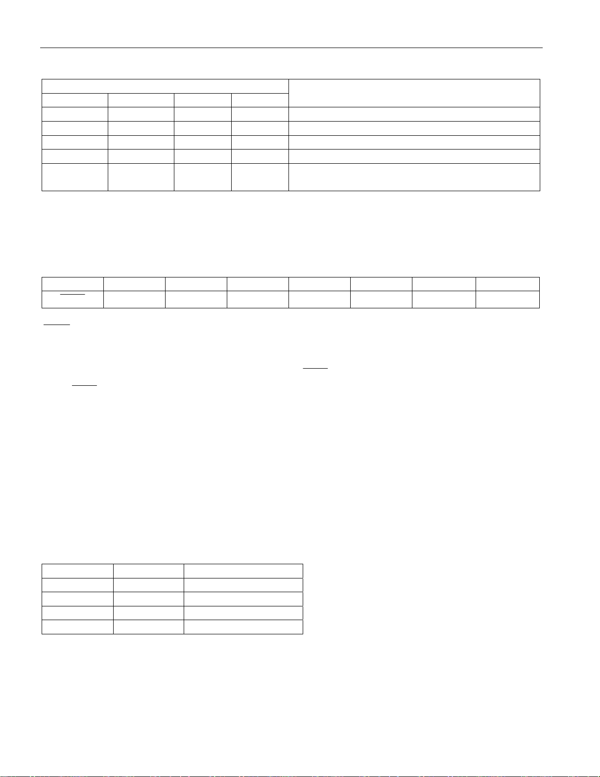
ORDERING INFORMATION
PART*
VOLTAGE
(V)
DS1673E-3 3.0 20 TSSOP DS1673-3
DS1673E-3+ 3.0 20 TSSOP DS1673-3
DS1673E-5 5.0 20 TSSOP DS1673-5
DS1673E-3/
T&R
DS1673E-3+
T&R
DS1673E-5/
T&R
3.0 20 TSSOP DS1673-3
3.0 20 TSSOP DS1673-3
5.0 20 TSSOP DS1673-5
DS1673S-3 3.0 20 SO DS1673S-3
DS1673S-5 5.0 20 SO DS1673S-5
* All devices are specified over the 0°C to +70°C operating range.
† A “‘+” anywhere on the top mark denotes a lead-free device.
+ Denotes a lead-free/RoHS-compliant device.
PINPACKAGE
TOP MARK†
DS1673
Portable System Controlle
FEATURES
§ Provides Real-Time Clock
Counts Seconds, Minutes, Hours, Date of the
Month, Month, Day of the Week, and Year
with Leap Year Compensation Valid Up to
2100
Power-Control Circuitry Supports System
Power-On from Day/Time Alarm
§ Microprocessor Monitor
Halts Microprocessor During Power Fail
Automatically Restarts Microprocessor after
Power Failure
Monitors Pushbutton for External Override
Halts and Resets an Out-of-Control
Microprocessor
§ NV RAM Control
Automatic Battery Backup and Write Protection
to External SRAM
§ 3-Channel, 8-Bit ADC
§ Simple 3-Wire Interface
§ +3.0V or +5.0V Operation
PIN CONFIGURATION
TOP VIEW
V
V
SCLK
CE
CEO
CEO
INT
GND
BAT
1
DS1673
CCO
I/O
CS
2
3
4
5
6
7
8
9
10
TSSOP (4.4mm)
SO (300 mils)
20
19
18
17
16
15
14
13
12
11
T
V
CC
X2
IN0
IN1
ST
1 of 18 REV: 080805
Page 2
DS1673
DETAILED DESCRIPTION
The microprocessor monitor circuitry of the DS1673 provides three basic functions. First, a precision
temperature-compensated reference and comparator circuit monitors the status of VCC. When an out-oftolerance condition occurs, an internal power-fail signal is generated which forces the reset to the active
state. When VCC returns to an in-tolerance condition, the reset signals are kept in the active state for
250 ms to allow the power supply and processor to stabilize. The second microprocessor monitor function
is pushbutton reset control. The DS1673 debounces a pushbutton input and guarantees an active reset
pulse width of 250 ms. The third function is a watchdog timer. The DS1673 has an internal timer that
forces the reset signals to the active state if the strobe input is not driven low prior to watchdog timeout.
The DS1673 also provides a 3-channel, 8-bit successive approximation analog-to-digital converter. The
converter has an internal 2.55V (typical) reference voltage generated by an on-board band-gap circuit.
The ADC is monotonic (no missing codes) and has an internal analog filter to reduce high frequency
noise.
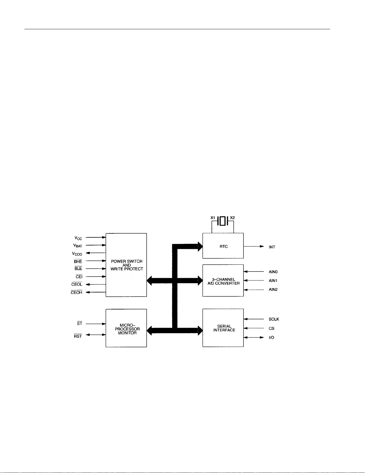
OPERATION
The block diagram in Figure 1 shows the main elements of the DS1673. The following paragraphs
describe the function of each pin.
DS1673 BLOCK DIAGRAM Figure 1
2 of 18
Page 3

PIN DESCRIPTION
PIN NAME FUNCTION
1 V
2 V
3 SCLK Serial Clock Input. Used to synchronize data movement on the serial interface.
4 I/O Data Input/Output. This pin is the bidirectional data pin for the 3-wire interface.
5 CS
6 CEI RAM Chip-Enable In. Must be driven low to enable the external RAM.
7 CEOL
8 CEOH
9 INT
10 GND Ground. DC power is provided to the device on this pin.
11 BHE
12 BLE
13
14,
15, 16
17, 18 X2, X1
19 VCC +3.0V or +5.0V Input DC Power
20 ST
Battery Input for Standard 3V Lithium Cell or Other Energy Source
BAT
External SRAM Power Supply Output. This pin is internally connected to V
CCO
is within nominal limits. However, during power-fail V
V
CC
to the V
pin. Switchover occurs when VCC drops below V
BAT
Chip Select. Must be asserted high during a read or a write for communication over the
3-wire serial interface. CS has an internal 40kW pulldown resistor.
RAM Chip-Enable Out Low. Active-low chip-enable output for low-order SRAM
byte.
RAM Chip-Enable Out High. Active-low chip-enable output for high-order SRAM
byte.
Interrupt Output. This pin is an active-high output that can be used as an interrupt
input to a microprocessor. The INT output remains high as long as the status bit
causing the interrupt is present and the corresponding interrupt-enable bit is set. The
INT pin operates when the DS1673 is powered by V
CC
or V
Byte High-Enable Input. This pin when driven low activates the CEOH output if CEI
is also driven low.
Byte Low-Enable Input. This pin when driven low activates the CEOL output if CEI is
also driven low.
Active-Low Reset. The RST pin functions as a microprocessor reset signal. This pin is
driven low 1) when VCC is outside of nominal limits; 2) when the watchdog timer has
RST
timed out; 3) during the power-up reset period; and 4) in response to a pushbutton
reset. The RST pin also functions as a pushbutton reset input. When the RST pin is
driven low, the signal is debounced and timed such that a RST signal of at least 250ms
is generated. This pin has an open-drain output with an internal 47kW pullup resistor.
AIN2,
AIN1,
Analog Inputs. These pins are the three analog inputs for the 3-channel ADC.
AIN0
Connections for Standard 32.768kHz Quartz Crystal. For greatest accuracy, the
DS1673 must be used with a crystal that has a specified load capacitance of 6pF. There
is no need for external capacitors or resistors. Note: X1 and X2 are very highimpedance nodes. It is recommended that they and the crystal be guard-ringed with
ground and that high frequency signals be kept away from the crystal area. For more
information on crystal selection and crystal layout considerations, refer to Application
Note 58: Crystal Considerations with Dallas Real Time Clocks. The DS1673 does not
function without a crystal.
Active-Low Strobe Input. The strobe input pin is used with the watchdog timer. If the
ST pin is not driven low within the watchdog time period, the RST pin is driven low.
is internally connected
CCO
.
CCSW
.
BAT
when
CC
DS1673
3 of 18
Page 4
POWER-UP/POWER-DOWN CONSIDERATIONS
When VCC is applied to the DS1673 and reaches a level greater than V
device becomes fully accessible after t
When VCC drops below V
, the device is switched over to the V
CCSW
(250ms typical). Before t
RPU
RPU
supply.
BAT
DS1673
(power-fail trip point), the
CCTP
elapses, all inputs are disabled.
During power-up, when V
returns to an in-tolerance condition, the RST pin is kept in the active state
CC
for 250ms (typical) to allow the power supply and microprocessor to stabilize.
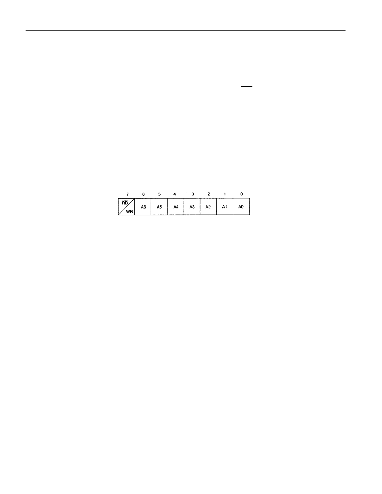
ADDRESS/COMMAND BYTE
The command byte for the DS1673 is shown in Figure 2. Each data transfer is initiated by a command
byte. Bits 0 through 6 specify the address of the registers to be accessed. The MSB (bit 7) is the
Read/Write bit. This bit specifies whether the accessed byte will be read or written. A read operation is
selected if bit 7 is a 0 and a write operation is selected if bit 7 is a one. The address map for the DS1673 is
shown in Figure 3.
ADDRESS/COMMAND BYTE Figure 2
4 of 18
Page 5
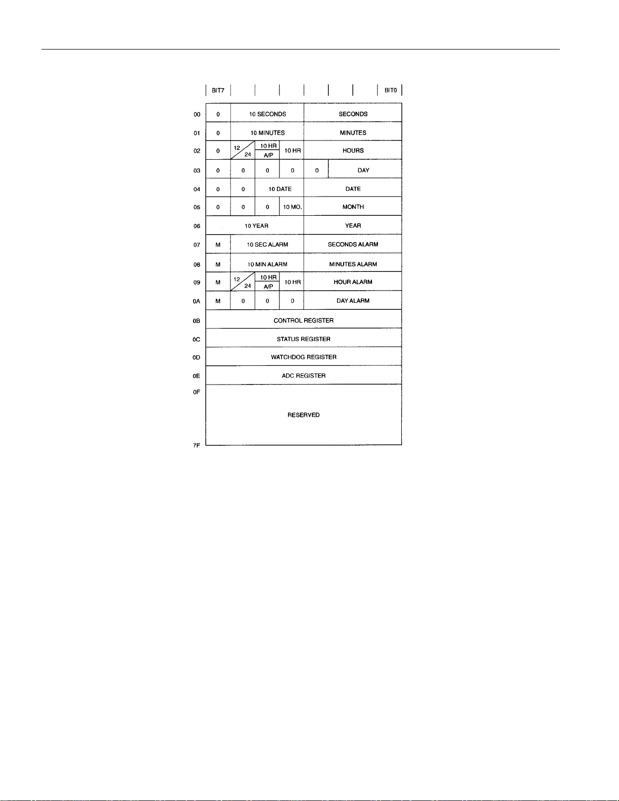
DS1673 ADDRESS MAP Figure 3
DS1673
CLOCK, CALENDAR, AND ALARM
The time and calendar information is accessed by reading/writing the appropriate register bytes. Note that
some bits are set to 0. These bits will always read 0 regardless of how they are written. Also note that
registers 0Fh to 7Fh are reserved. These registers will always read 0 regardless of how they are written.
The contents of the time, calendar, and alarm registers are in the Binary-Coded Decimal (BCD) format.
The DS1673 can run in either 12-hour or 24-hour mode. Bit 6 of the hours register is defined as the 12- or
24-hour mode select bit. When high, the 12-hour mode is selected. In the 12-hour mode, bit 5 is the
AM/PM bit with logic 1 being PM. In the 24-hour mode, bit 5 is the second 10-hour bit (20-23 hours).
The DS1673 also contains a time of day alarm. The alarm registers are located in registers 07h to 0Ah.
Bit 7 of each of the alarm registers are mask bits (see Table 1). When all of the mask bits are logic 0, an
alarm will occur once per week when the values stored in timekeeping registers 00h to 03h match the
values stored in the time of day alarm registers. An alarm will be generated every day when mask bit of
the day alarm register is set to 1. An alarm will be generated every hour when the day and hour alarm
mask bits are set to 1. Similarly, an alarm will be generated every minute when the day, hour, and minute
alarm mask bits are set to 1. When day, hour, minute, and seconds alarm mask bits are set to 1, an alarm
will occur every second.
5 of 18
Page 6
DS1673
TIME OF DAY ALARM BITS Table 1
ALARM REGISTER MASK BITS (BIT 7)
SECONDS MINUTES HOURS DAYS
1 1 1 1 Alarm once per second.
0 1 1 1 Alarm when seconds match.
0 0 1 1 Alarm when minutes and seconds match.
0 0 0 1 Alarm when hours, minutes and seconds match.
0 0 0 0 Alarm when day, hours, minutes and seconds
match.
DESCRIPTION
SPECIAL PURPOSE REGISTERS
The DS1673 has two additional registers (control register and status register) that control the RTC and
interrupts.
CONTROL REGISTER
BIT 7 BIT 6 BIT 5 BIT 4 BIT 3 BIT 2 BIT 1 BIT 0
EOSC
WP AIS1 AIS0 0 0 0 AIE
EOSC (Enable Oscillator). This bit, when set to logic 0 will start the oscillator. When this bit is set to a
logic 1, the oscillator is stopped and the DS1673 is placed into a low-power standby mode with a current
drain of less than 200nA when in battery-backup mode. When the DS1673 is powered by VCC, the
oscillator is always on regardless of the status of the EOSC bit; however, the RTC is incremented only
when EOSC is a logic 0.
WP (Write Protect). Before any write operation to the RTC or any other registers, this bit must be logic
0. When high, the write protect bit prevents a write operation to any register.
AIS0-AIS1 (Analog Input Select). These 2 bits are used to determine the analog input for the analog-todigital conversion. Table 2 lists the specific analog input that is selected by these 2 bits.
AIE (Alarm Interrupt Enable). When set to a logic 1, this bit permits the Interrupt Request Flag (IRQF)
bit in the status register to assert INT. When the AIE bit is set to logic 0, the IRQF bit does not initiate the
INT signal.
ANALOG INPUT SELECTION Table 2
AIS1 AIS0 ANALOG INPUT
0 0 NONE
0 1 AIN0
1 0 AIN1
1 1 AIN2
6 of 18
Page 7

DS1673
STATUS REGISTER
BIT 7 BIT 6 BIT 5 BIT 4 BIT 3 BIT 2 BIT 1 BIT 0
CU LOBAT 0 0 0 0 0 IRQF
CU (Conversion Update In Progress). When this bit is a 1, an update to the ADC Register (register
0Eh) will occur within 488ms. When this bit is a 0, an update to the ADC Register will not occur for at
least 244ms.
LOBAT (Low Battery Flag). This bit reflects the status of the backup power source connected to the
V
pin. When V
BAT
is greater than 2.5V, LOBAT is set to a logic 0. When V
BAT
is less than 2.3V,
BAT
LOBAT is set to a logic 1.
IRQF (Interrupt Request Flag). A logic 1 in the Interrupt Request Flag bit indicates that the current
time has matched the time of day Alarm registers. If the AIE bit is also a logic 1, the INT pin will go
high. IRQF is cleared by reading or writing to any of the alarm registers.
POWER-UP DEFAULT STATES
These bits are set to a one upon initial power-up: EOSC , TD1 and TD0. These bits are cleared upon
initial power-up: WP, AIS1, and AIS0.
NONVOLATILE SRAM CONTROLLER
The DS1673 provides automatic backup and write protection for external SRAM. This function is
provided by gating the chip enable signals and by providing a constant power supply through the V
pin. The DS1673 was specifically designed with the Intel 80186 and 386EX microprocessors in mind. As
such, the DS1673 has the capability to provide access to the external SRAM in either byte-wide or wordwide format. This capability is provided by the chip enable scheme. Three input signals and two output
CCO
signals are used for enabling the external SRAM(s) (see Figure 4).
enable), and
CEOL (chip enable low) and the CEOH (chip enable high) outputs. Table 3 illustrates the function of
BLE (byte low enable) are used for enabling either one or two external SRAMs through the
CEI (chip enable in), BHE (byte high
these pins.
The DS1673 nonvolatilizes the external SRAM(s) by write-protecting the SRAM(s) and by providing a
back-up power supply in the absence of V
are prohibited by forcing
CEOL and CEOH high regardless of the level of CEI , BLE , and BHE . Upon
power-up, access is prohibited until the end of t
. When VCC falls below VPF, access to the external SRAM(s)
CC
.
RPU
EXTERNAL SRAM CHIP ENABLE Table 3
CEI
BHE BLE
CEOL CEOH
0 0 0 0 0 Word transfer
0 0 1 1 0 Byte transfer in upper half of data bus (D15-D8)
0 1 0 0 1 Byte transfer in lower half of data bus (D7-D0)
0 1 1 1 1 External SRAMs disabled
1 X X 1 1 External SRAMs disabled
FUNCTION
7 of 18
Page 8

DS1673
EXTERNAL SRAM INTERFACE (WORD-WIDE) TO THE DS1673 Figure 4
MICROPROCESSOR MONITOR
The DS1673 monitors three vital conditions for a microprocessor: power supply, software execution, and
external override.
First, a precision temperature-compensated reference and comparator circuit monitors the status of V
When an out-of-tolerance condition occurs, an internal power-fail signal is generated which forces the
CC
.
RST pin to the active state, thus warning a processor-based system of impending power failure. When
V
returns to an in-tolerance condition upon power-up, the reset signal is kept in the active state for
CC
250ms (typical) to allow the power supply and microprocessor to stabilize. Note, however, that if the
EOSC bit is set to a logic 1 (to disable the oscillator during battery-backup mode), the reset signal will be
kept in an active state for 250 ms plus the start-up time of the oscillator.
The second monitoring function is push-button reset control. The DS1673 provides for a pushbutton
switch to be connected to the
monitors the
switch by pulling the
to monitor the
RST signal for a low going edge. If an edge is detected, the DS1673 will debounce the
RST line low. After the internal 250ms timer has expired, the DS1673 will continue
RST line. If the line is still low, the DS1673 will continue to monitor the line looking for a
rising edge. Upon detecting release, the DS1673 will force the
RST output pin. When the DS1673 is not in a reset cycle, it continuously
RST line low and hold it low for 250ms.
The third microprocessor monitoring function provided by the DS1673 is a watchdog timer. The
watchdog timer function forces
RST to the active state when the ST input is not stimulated within the
predetermined time period. The time period is set by the Time Delay (TD) bits in the Watchdog Register.
The time delay can be set to 250ms, 500ms, or 1000ms (see Figure 5). If TD0 and TD1 are both set to
zero, the watchdog timer is disabled. When enabled, the watchdog timer starts timing out from the set
time period as soon as
RST is inactive. The default setting is for the watchdog timer to be enabled with
1000ms time delay. If a high-to-low transition occurs on the
timer is reset and begins to time-out again. If the watchdog timer is allowed to time-out, then the
signal is driven to the active state for 250ms (typical). The
ST input pin prior to time-out, the watchdog
RST
ST input can be derived from microprocessor
address signals, data signals, and/or control signals. To guarantee that the watchdog timer does not timeout, a high-to-low transition must occur at or less than the minimum period.
8 of 18
Page 9

DS1673
WATCHDOG TIME-OUT CONTROL Figure 5
WATCHDOG REGISTER
BIT 7 BIT 6 BIT 5 BIT 4 BIT 3 BIT 2 BIT 1 BIT 0
0 0 0 0 0 0 TD1 TD0
WATCHDOG REGISTER
TD1 TD0 WATCHDOG TIME-OUT
0 0 WATCHDOG DISABLED
0 1 250 ms
1 0 500 ms
1 1 1000 ms
ANALOG-TO-DIGITAL CONVERTER
The DS1673 provides a 3-channel, 8-bit analog-to-digital converter. The ADC reference voltage (2.55V
typical) is derived from an on-chip band-gap circuit. Three multiplexed analog inputs are provided
through the AIN0, AIN1, and AIN2 pins. The ADC is monotonic (no missing codes) and uses a
successive approximation technique to convert the analog signal into a digital code.
An A/D conversion is the process of assigning a digital code to an analog input voltage. This code
represents the input value as a fraction of the full-scale voltage (FSV) range. Thus, the FSV range is then
divided by the ADC into 256 codes (8 bits). The FSV range is bounded by an upper limit equal to the
reference voltage and the lower limit, which is ground. The DS1673 has a FSV of 2.55V (typical) that
provides a resolution of 10mV. An input voltage equal to the reference voltage converts to FFh while an
input voltage equal to ground converts to 00h. The relative linearity of the ADC is
The A/D converter selects from one of three different analog inputs (AIN0–AIN2). The input that is
selected is determined by the Analog Input Select (AIS) bits in the Control Register. Table 2 lists the
specific analog input that is selected by these 2 bits. Note also that the converter can be turned off by
these bits to reduce power. When the ADC is turned on by setting AIS0 and AIS1 to any value other than
0,0 the analog input voltage is converted and written to the ADC Register within 488
analog filter at the input reduces high frequency noise. Subsequent updates occur approximately every
10ms. If AIS0 and/or AIS1 are changed, updates will occur at the next 10 ms conversion time.
The Conversion Update In Progress (CU) bit in the Status Register indicates when the ADC Register can
be read. When this bit is a 1, an update to the ADC Register will occur within 488
when this bit is 0 an update will not occur for at least 244
ms. The CU bit should be polled before reading
the ADC Register to insure that the contents are stable during a read cycle. Once a read cycle to the ADC
Register has been started, the DS1673 will not update that register until the read cycle has been
completed. It should also be mentioned that taking CS low will abort the read cycle and will allow the
ADC Register to be updated.
Figure 6 illustrates the timing of the CU bit relative to an instruction to begin conversion and the
completion of that conversion.
±0.5 LSB.
ms. An internal
ms maximum. However,
9 of 18
Page 10

DS1673
CU BIT TIMING Figure 6
3-WIRE SERIAL INTERFACE
Communication with the DS1673 is accomplished through a simple 3-wire interface consisting of the
Chip Select (CS), Serial Clock (SCLK) and Input/Output (I/O) pins.
All data transfers are initiated by driving the CS input high. The CS input serves two functions. First, CS
turns on the control logic, which allows access to the shift register for the address/command sequence.
Second, the CS signal provides a method of terminating either single byte or multiple byte (burst) data
transfer. A clock cycle is a sequence of a rising edge followed by a falling edge. For data input, data must
be valid during the rising edge of the clock and data bits are output on the falling edge of the clock. If the
CS input goes low, all data transfer terminates and the I/O pin goes to a high impedance state.
Address and data bytes are always shifted LSB first into the I/O pin. Any transaction requires the
address/command byte to specify a read or write to a specific register followed by 1 or more bytes of
data. The address byte is always the first byte entered after CS is driven high. The most significant bit
(
RD /WR) of this byte determines if a read or write will take place. If this bit is 0, one or more read cycles
will occur. If this bit is 1, one or more write cycles will occur.
Data transfers can occur 1 byte at a time or in multiple byte burst mode. After CS is driven high an
address is written to the DS1673. After the address, 1 or more data bytes can be read or written. For a
single-byte transfer 1 byte is read or written and then CS is driven low. For a multiple-byte transfer,
multiple bytes can be read or written to the DS1673 after the address has been written. Each read or write
cycle causes the register address to automatically increment. Incrementing continues until the device is
disabled. After accessing register 0Eh, the address wraps to 00h.
Data transfer for single-byte transfer and multiple-byte burst transfer is illustrated in Figures 7 and 8.
10 of 18
Page 11

SINGLE-BYTE DATA TRANSFER Figure 7
MULTIPLE-BYTE BURST TRANSFER Figure 8
DS1673
11 of 18
Page 12
DS1673
ABSOLUTE MAXIMUM RATINGS
Voltage on Any Pin Relative to Ground…………………………………………………….-0.3V to +7.0V
Operating Temperature………………………………………………………………………..0°C to +70°C
Storage Temperature……………………………………………………………………….-55°C to +125°C
Soldering Temperature………………………………………………………..See J-STD-020 Specification
This is a stress rating only and functional operation of the device at these or any other conditions above those indicated in the
operation sections of this specification is not implied. Exposure to absolute maximum rating conditions for extended periods of
time may affect device reliability.
RECOMMENDED DC OPERATING CONDITIONS (TA = 0°C to +70°C)
PARAMETER SYMBOL MIN TYP MAX UNITS NOTES
Power Supply Voltage
5.0V 4.5 5.0 5.5
3.0V
VCC
2.7 3.0 3.3
V 1
Input Logic 1 VIH 2.0 VCC+0.3 V 1
Input Logic 0 VIL -0.3 +0.8 V 1
Battery Voltage V
2.5 3.7 V 1
BAT
DC ELECTRICAL CHARACTERISTICS (VCC = 5.0V ±10%, TA = 0°C to +70°C.)
PARAMETER SYMBOL MIN TYP MAX UNITS NOTES
Input Leakage ILI -1 +1
CS Leakage ILO 150
Logic 1 Output (I
Logic 0 Output (I
Active Supply Current (CS = VCC - 0.2) I
A/D Converter Current I
Standby Current (CS = VIL) I
Battery Current (Oscillator On) I
Battery Current (Oscillator Off) I
Internal RST Pullup Resistor
VCC Trip Point V
VCC Switchover V
A/D Reference Voltage V
= -0.4mA) VOH 2.4 V 2
OUT
= 1.5mA) VOL 0.4 V 3
OUT
1.5 2.0 mA 4
CCA
500
ADC
300
CCS
300 500 nA
BAT1
200 nA
BAT2
R
35 47 60
P
4.25 4.35 4.50 V
CCTP
2.60 2.70 2.80 V 12
CCSW
2.47 2.55 2.63 V
ADC
mA
mA
mA
mA
W
k
Pushbutton Detect PBDV 0.8 2.0 V
Pushbutton Release PBRD 0.3 0.8 V
Output Voltage V
V
Output Current (Source = VCC) I
CCO
V
Output Current (Source = V
CCO
) I
BAT
VCC-0.3 V 11
CCO
150 mA 13
CCO1
150
CCO2
mA
7
5
6
14
12 of 18
Page 13

DS1673
DC ELECTRICAL CHARACTERISTICS (VCC = 3.0V ±10%, TA = 0°C to +70°C.)
PARAMETER SYMBOL MIN TYP MAX UNITS NOTES
Input Leakage
CS Leakage
Logic 1 Output (I
Logic 0 Output (I
=-0.4mA) VOH 2.4 V 2
OUT
= 1.5mA) VOL 0.4 V 3
OUT
Active Supply Current (CS = VCC - 0.2) I
ADC Current
Standby Current (CS = VIL)
Battery Current (Oscillator On) I
Battery Standby Current (Oscillator Off) I
Internal RST Pullup Resistor
VCC Trip Point V
VCC Switchover V
A/D Reference Voltage V
I
-1 +1
LI
I
150
LO
0.75 1.0 mA 4
CCA
I
200
ADC
I
100
CCS
300 500 nA
BAT1
200 nA
BAT2
R
35 47 60
P
2.5 2.6 2.7 V
CCTP
2.30 2.40 2.50 V 12
CCSW
2.47 2.55 2.63 V
ADC
mA
mA
mA
mA
W
k
7
5
6
Pushbutton Detect PBDV 0.8 2.0 V
Pushbutton Release PBRD 0.3 0.8 V
Output Voltage V
V
Output Current (Source = VCC) I
CCO
V
Output Current (Source = V
CCO
BAT
)
VCC-0.3 V 11
CCO
80 mA 13
CCO1
I
100
CCO2
mA
14
CAPACITANCE (TA = +25°C)
PARAMETER SYMBOL MIN TYP MAX UNITS NOTES
Input Capacitance CI 10 pF
I/O Capacitance C
Crystal Capacitance CX 6 pF
15 pF
I/O
13 of 18
Page 14

DS1673
AC ELECTRICAL CHARACTERISTICS (VCC = 5.0V ±10%, TA = 0°C to 70°C.)
PARAMETER SYMBOL MIN TYP MAX UNITS NOTES
Data to Clock Setup tDC 50 ns 8
CLK to Data Hold t
CLK to Data Delay t
CLK to Low Time tCL 250 ns 8
CLK to High Time tCH 250 ns 8
CLK Frequency t
CLK Rise and Fall tR, tF 500 ns
CS to CLK Setup tCC 1
CLK to CS Hold t
CS Inactive Time t
CS to I/O High-Z t
VCC Slew Rate (4.5V to 2.3V) tF 1 ms
VCC Slew Rate (2.3V to 4.5V) tR 0 ns
VCC Detect to RST (VCC Falling)
Reset Active Time t
Pushbutton Debounce PBDB 250 ms 15
VCC Detect to RST (VCC Rising)
ST Pulse Width
Chip Enable Propagation Delay to
External SRAM
Nominal Voltage to VCC Switchover
Fall Time
70 ns 8
CDH
200 ns 8, 9, 10
CDD
2.0 MHz 8
CLK
ms
60 ns 8
CCH
1
CWH
70 ns 8
CDZ
t
100 ns
RPD
250 ms 15
RST
t
250 ms 15, 16
RPU
t
20 ns
ST
8 15 ns
t
CED
200
t
FB
ms
ms
8
8
14 of 18
Page 15

DS1673
AC ELECTRICAL CHARACTERISTICS (VCC = 3.0V ±10%, TA = 0°C to +70°C.)
PARAMETER SYMBOL MIN TYP MAX UNITS NOTES
Data to Clock Setup tDC 150 ns 8
CLK to Data Hold t
CLK to Data Delay t
CLK to Low Time tCL 750 ns 8
CLK to High Time tCH 750 ns 8
CLK Frequency t
CLK Rise and Fall tR, tF 1500 ns
CS to CLK Setup tCC 3
CLK to CS Hold t
CS Inactive Time t
CS to I/O High-Z t
VCC Slew Rate (2.7V to 2.3V) tF 300
VCC Slew Rate (2.3V to 2.7V) tR 0 ns
VCC Detect to RST (VCC Falling)
Reset Active Time t
Pushbutton Debounce PBDB 250 ms 15
VCC Detect to RST (VCC Rising)
ST Pulse Width
Chip Enable Propagation Delay to
External SRAM
Nominal Voltage to VCC Switchover
Fall Time
210 ns 8
CDH
600 ns 8, 9, 10
CDD
0.667 MHz 8
CLK
ms
180 ns 8
CCH
3
CWH
210 ns 8
CDZ
ms
ms
t
200 ns
RPD
250 ms 15
RST
t
250 ms 15, 16
RPU
t
40 ns
ST
8 25 ns
t
CED
300
t
FB
ms
8
8
15 of 18
Page 16

TIMING DIAGRAM: READ DATA Figure 9
TIMING DIAGRAM: WRITE DATA Figure 10
DS1673
16 of 18
Page 17

PUSHBUTTON RESET Figure 11
POWER-UP Figure 12
POWER-DOWN Figure 13
DS1673
17 of 18
Page 18

NOTES:
1. All voltages are referenced to ground.
DS1673
2. Logic 1 voltages are specified at V
3. Logic 0 voltages are specified at V
4. I
is specified with outputs open, CS set to a logic 1, SCLK = 500kHz, oscillator enabled, and
CCA
= 3.0V, VOH = VCC for capacitive loads. Excludes
CC
= 3.0V, VOL = GND for capacitive loads.
CC
RST
pin
D/A converter enabled.
5. I
6. I
7. CS has a 40k
8. Measured at V
9. Measured at V
is specified with CS, V
ADC
is specified with CS, V
CCS
W pulldown resistor to ground.
= 2.0V or VIL = 0.8V and 10ns maximum rise and fall time.
IH
= 2.4V or VOL = 0.4V.
OH
open and I/O, SCLK at logic 0. ADC is enabled.
CCO
open and I/O, SCLK at logic 0. ADC is disabled.
CCO
10. Load capacitance = 25pF.
11. I
12. V
= 100mA, VCC > V
CCO
switchover from VCC to V
CCO
13. Current from V
14. Current from V
input pin to V
CC
input pin to V
BAT
CCTP
.
occurs when VCC drops below the lower of V
BAT
output pin.
CCO
output pin.
CCO
CCSW
and V
BAT
.
15. Time base is generated by very accurate crystal oscillator. Accuracy of this time period is based on
the crystal that is used. A typical crystal with a specified load capacitance of 6pF will provide an
accuracy within ±100ppm over the 0°C to +70°C temperature range.
16. If the
EOSC bit in the Control Register is set to a logic 1, t
is equal to 250ms plus the startup
RPU
time of the crystal oscillator.
PACKAGE INFORMATION
(For the latest package outline information, go to www.maxim-ic.com/DallasPackInfo.)
18 of 18
Maxim/Dallas Semiconductor cannot assume responsibility for use of any circuitry other than circuitry entirely embodied in a Maxim/Dallas Semiconductor product.
No circuit patent licenses are implied. Maxim/Dallas Semiconductor reserves the right to change the circuitry and specifications without notice at any time.
Maxim Integrated Products, 120 San Gabriel Drive, Sunnyvale, CA 94086 408-737-7600
The Maxim logo is a registered trademark of Maxim Integrated Products, Inc. The Dallas logo is a registered trademark of Dallas Semiconductor Corporation.
© 2005 Maxim Integrated Products · Printed USA
 Loading...