

R
www.maxim-ic.com
DS1672
2
C 32-Bit Binary Counter RTC
I
GENERAL DESCRIPTION
The DS1672 incorporates a 32-bit counter and
power-monitoring functions. The 32-bit counter
is designed to count seconds and can be used to
derive time-of-day, week, month, month, and
year by using a software algorithm. A precision,
temperature-compensated reference and
comparator circuit monitors the status of VCC.
When an out-of-tolerance condition occurs, an
internal power-fail signal is generated that forces
the reset to the active state. When VCC returns to
an in-tolerance condition, the reset signal is kept
in the active state for a period of time to allow
the power supply and processor to stabilize.
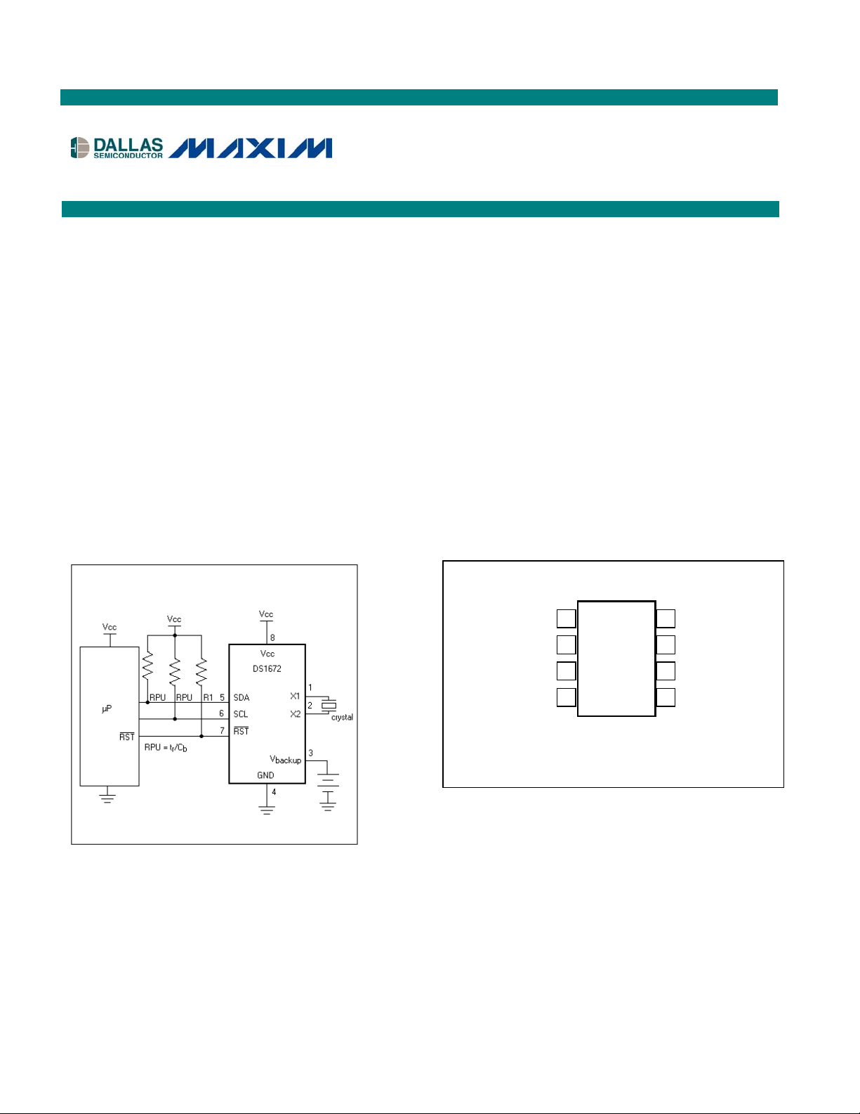
TYPICAL OPERATING CIRCUIT
FEATURES
32-Bit Counter
I2C* Serial Interface
Automatic Power-Fail Detect and Switch
Circuitry
Power-Fail Reset Output
Low-Voltage Oscillator Operation
(1.3V min)
Trickle-Charge Capability
Underwriters Laboratory (UL) Recognized
-40°C to +85°C Operating Temperature
Range
PIN CONFIGURATION
TOP VIEW
V
BACKUP
X1
X2
GND
*Purchase of I2C components from Maxim Integrated Products,
Inc., or one of its sublicensed Associated Companies, conveys a
license under the Philips I
components in an I
to the I
2
2
C Standard Specification defined by Philips.
1
DS1672
2
3
4
µSOP
2
C system, provided that the system conforms
8
7
6
5
DIP
SO
C Patent Rights to use these
V
CC
ST
SCL
SDA
1 of 15 REV: 031406
ORDERING INFORMATION
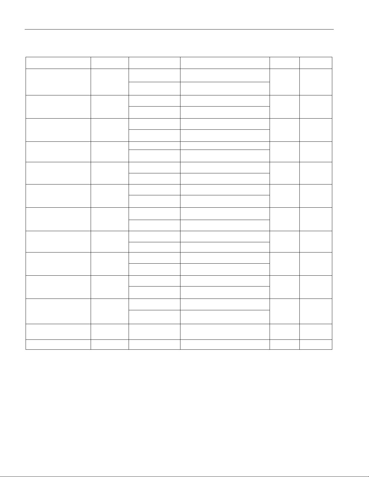
PART TEMP RANGE VOLTAGE (V) PIN-PACKAGE TOP MARK*
DS1672-2 -40°C to +85°C 2.0 8 DIP (300 mils) DS1672-2
DS1672-3 -40°C to +85°C 3.0 8 DIP (300 mils) DS1672-3
DS1672-33 -40°C to +85°C 3.3 8 DIP (300 mils) DS1672-33
DS1672S-2 -40°C to +85°C 2.0 8 SO (150 mils) DS1672-2
DS1672S-2+ -40°C to +85°C 2.0 8 SO (150 mils) D1672-2
DS1672S-3 -40°C to +85°C 3.0 8 SO (150 mils) DS1672-3
DS1672S-3+ -40°C to +85°C 3.0 8 SO (150 mils) D1672-3
DS1672S-33 -40°C to +85°C 3.3 8 SO (150 mils) DS167233
DS1672S-33+ -40°C to +85°C 3.3 8 SO (150 mils) D167233
DS1672
DS1672S-3/T&R -40°C to +85°C 3.0
DS1672S-3+T&R -40°C to +85°C 3.0
DS1672S-33/T&R -40°C to +85°C 3.3
DS1672S-33+T&R -40°C to +85°C 3.3
DS1672U-2 -40°C to +85°C 2.0
DS1672U-2+ -40°C to +85°C 2.0
DS1672U-3 -40°C to +85°C 3.0
DS1672U-3+ -40°C to +85°C 3.0
DS1672U-33 -40°C to +85°C 3.3
DS1672U-33+ -40°C to +85°C 3.3
DS1672U-33/T&R -40°C to +85°C 3.3
DS1672U-33+T&R -40°C to +85°C 3.3
8 SO (150 mils)/Tape
and Reel
8 SO (150 mils)/Tape
and Reel
8 SO (150 mils)/Tape
and Reel
8 SO (150 mils)/Tape
and Reel
8 µSOP (3mm)
8 µSOP (3mm)
8 µSOP (3mm)
8 µSOP (3mm)
8 µSOP (3mm)
8 µSOP (3mm)
8 µSOP (3mm)/Tape
and Reel
8 µSOP (3mm)/Tape
and Reel
DS1672-3
D1672-3
DS167233
D167233
1672
rr -2
1672
rr -2
1672
rr -3
1672
rr -3
1672
rr -33
1672
rr -33
1672
rr -33
1672
rr -33
+ Denotes a lead-free/RoHS-compliant device.
* A “+” anywhere on the top mark denotes a lead-free device. rr = 2-digit alphanumeric revision code.
2 of 15
DS1672
ABSOLUTE MAXIMUM RATINGS
Voltage Range on Any Pin Relative to Ground……………………………………………..-0.5V to +6.0V
Operating Temperature Range (noncondensing) ...…………………………………………-40°C to +85°C
Storage Temperature Range……………………………………………………………….-55°C to +125°C
Soldering Temperature………………………………………….See IPC/JEDEC J-STD-020 Specification
This is a stress rating only and functional operation of the device at these or any other conditions beyond those indicated in the operation
sections of this specification is not implied. Exposure to absolute maximum rating conditions for extended periods of time can affect device
reliability.
RECOMMENDED DC OPERATING CONDITIONS
(TA = -40°C to +85°C)
PARAMETER SYMBOL MIN TYP MAX UNITS NOTES
Supply
Voltage
Logic 1 VIH 0.7 x VCC V
DS1672-2 VCC 1.8 2.0 2.2
DS1672-3 VCC 2.7 3.0 3.3
DS1672-33 V
2.97 3.3 3.63
CC
+ 0.5 V 1
CC
V 1
Logic 0 VIL -0.5 +0.3 x VCC V 1
Backup Supply Voltage V
1.3 3.0 3.63 V 1
BACKUP
DC ELECTRICAL CHARACTERISTICS
(V
Active Supply Current I
Standby Current I
Power-Fail Voltage VPF
CCMIN
< VCC < V
CCMAX, TA
= -40°C to +85°C.)
PARAMETER SYMBOL MIN TYP MAX UNITS NOTES
600
CCA
500
CCS
µA
µA
2
3
2.70 2.88 2.97
2.45 2.6 2.7
V
1.58 1.7 1.8
V
Leakage Current I
BACKUP
BACKUPLKG
25 50 nA
Logic 0 Output (VOL = 0.4V) IOL 3 mA 1, 4
Logic 0
Output
(DS1672-2)
Note 1: All voltages referenced to ground.
Note 2: I
Note 3: I
Note 4: SDA and RST.
specified with SCL clocking at max frequency (400kHz), trickle charger disabled.
CCA
specified with VCC = V
CCS
(VCC > 2V;
V
= 0.4V)
OL
< 2V;
(V
CC
V
= 0.2 x VCC)
OL
CCTYP
I
OL
and SDA, SCL = V
CCTYP
3
mA 1, 4
3
, trickle charger disabled.
3 of 15
DS1672
DC ELECTRICAL CHARACTERISTICS
(VCC = 0V, TA = -40°C to +85°C.)
PARAMETER SYMBOL MIN TYP MAX UNITS NOTES
V
V
Note 5: Using the recommended crystal on X1 and X2.
Current (Oscillator On) I
BACKUP
Current (Oscillator Off) I
BACKUP
BACKUPOSC
BACKUP
0.425 1
µA
5
200 nA
CRYSTAL SPECIFICATIONS
PARAMETER SYMBOL MIN TYP MAX UNITS NOTES
Nominal Frequency fO 32.768 kHz
Series Resistance ESR 45 kΩ
Load Capacitance CL 6 pF
*The crystal, traces, and crystal input pins should be isolated from RF generating signals. Refer to Application Note 58: Crystal
Considerations for Dallas Real-Time Clocks for additional specifications
*
4 of 15
DS1672
AC ELECTRICAL CHARACTERISTICS
(VCC = 0V, TA = -40°C to +85°C.)
PARAMETER SYMBOL CONDITIONS MIN TYP MAX UNITS NOTES
SCL Clock
Frequency
Bus Free Time
Between a STOP and
START Condition
Hold Time
(Repeated) START
Condition
LOW Period of SCL
Clock
HIGH Period of SCL
Clock
Setup Time for a
Repeated START
Condition
Data Hold Time t
Data Setup Time t
Rise Time of Both
SDA and SCL
Signals
Fall Time of Both
SDA and SCL
Signals
Setup Time for STOP
Condition
f
SCL
t
BUF
t
HD:STA
t
LOW
t
HIGH
t
SU:STA
HD:DAT
SU:DAT
t
R
t
F
t
SU:STO
Fast mode 100 400
kHz
Standard mode 100
Fast mode 1.3
µs
Standard mode 4.7
Fast mode 0.6
µs
6
Standard mode 4.0
Fast mode 1.3
Standard mode 4.7
µs
Fast mode 0.6
µs
Standard mode 4.0
Fast mode 0.6
µs
Standard mode 4.7
Fast mode 0 0.9
µs
7, 8
Standard mode 0
Fast mode 100
ns 9
Standard mode 250
Fast mode 20 + 0.1CB 300
ns 10
Standard mode 1000
Fast mode 20 + 0.1CB 300
ns 10
Standard mode 300
Fast mode 0.6
µs
Standard mode 4.0
Capacitive Load for
Each Bus Line
I/O Capacitance C
Note 6: After this period, the first clock pulse is generated.
Note 7: A device must internally provide a hold time of at least 300ns for the SDA signal (referenced to the V
order to bridge the undefined region of the falling edge of SCL.
Note 8:The maximum t
Note 9: A fast-mode device can be used in a standard-mode system, but the requirement t
automatically be the case if the device does not stretch the LOW period of the SCL signal. If such a device does stretch the LOW
period of the SCL signal, it must output the next data bit to the SDA line t
line is released.
Note 10: C
–Total capacitance of one bus line in pF.
B
has only to be met if the device does not stretch the LOW period (t
HD:DAT
400 pF 10
C
B
10 pF
I/O
) of the SCL signal.
LOW
≥ to 250ns must then be met. This will
SU:DAT
max + t
R
= 1000 + 250 = 1250ns before the SCL
SU:DAT
5 of 15
of the SCL signal) in
IHMIN

POWER-UP/POWER-DOWN CHARACTERISTICS
R
(TA = -40°C to +85°C)
PARAMETER SYMBOL MIN TYP MAX UNITS NOTES
t
VCC Detect to RST (VCC Falling)
VCC Detect to RST (VCC Rising)
VCC Fall Time; V
PF(MAX)
to V
PF(MIN)
t
10 µs
RPD
t
250 ms 11
RPU
300
F
µs
DS1672
VCC Rise Time; V
Note 11: If the EOSC bit in the control register is set to logic 1, t
PF(MIN)
to V
t
PF(MAX)
0
R
is equal to 250ms plus the startup time of the crystal oscillator.
RPU
µs
Warning: Negative undershoots below –0.3V while the part is in battery-backed mode can cause
loss of data.
Figure 1. Timing Diagram
SDA
t
BUF
t
SCL
STOP
START
LOW
t
HD:STA
t
HD:DAT
t
HIGH
t
F
t
t
SU:DAT
SU:STA
REPEATED
START
t
HD:STA
t
SU:STO
Figure 2. Power-Up/Power-Down Timing
V
PF(max)
V
PF(min)
V
CC
t
F
t
PD
t
RPD
t
R
t
RPU
ST
INPUTS
RECOGNIZED
DON'T CARE
RECOGNIZED
HIGH IMPEDANCE
OUTPUTS
VALID
VALID
6 of 15

PIN DESCRIPTION
PIN NAME FUNCTION
Connections for Standard 32.768kHz Quartz Crystal. The internal oscillator
circuitry is designed for operation with a crystal having a specified load
capacitance (CL) of 6pF. For more information about crystal selection and
1, 2 X1, X2
crystal layout considerations, refer to Application Note 58: Crystal
Considerations with Dallas Real-Time Clocks. The DS1672 can also be driven
by an external 32.768kHz oscillator. In this configuration, the X1 pin is
connected to the external oscillator signal and the X2 pin is floated.
Battery Input for Any Standard 3V Lithium Cell or Other Energy Source.
Battery voltage must be held between 1.3V and 3.63V for proper operation.
Diodes placed in series between the power source and the V
3 V
BACKUP
in improper operation. If a backup supply is not required, V
grounded. UL recognized to ensure against reverse charging current when used
in conjunction with a lithium battery (charger disabled). See “Conditions of
Acceptability” at www.maxim-ic.com/qa/info/ul.
4 GND Ground. DC power is provided to the device on this pin.
BACKUP
BACKUP
DS1672
may result
must be
5 SDA
6 SCL
Serial-Data Input/Output. SDA is the input/output pin for the I2C serial
interface. The SDA pin is open drain and requires an external pullup resistor.
I2C Serial-Clock Input. SCL is used to synchronize data movement on the
serial interface and requires an external pullup resistor.
Active-Low Reset Output. It functions as a microprocessor reset signal. This
7
RST
pin is an open-drain output and requires an external pullup resistor.
Power Pin for Primary Power Supply. When VCC is applied within normal
8 VCC
limits, the device is fully accessible and data can be written and read. When
VCC is below VPF, reads and writes are inhibited.
Figure 3. Recommended Layout for Crystal
LOCAL GROUND PLANE (LAYER 2)
X1
CRYSTAL
X2
GND
7 of 15

DS1672
R
DETAILED DESCRIPTION
The DS1672 provides a 32-bit counter that increments once-per-second. The counter data is accessible
via an I2C serial interface. A precision, temperature-compensated, voltage reference and comparator
circuit monitors V
. When VCC drops below VPF, RST becomes active and the interface is disabled to
CC
prevent data corruption. The device switches to the backup supply input, which maintains oscillator and
counter operation while V
(t
) to allow VCC to stabilize.
RPU
is absent. When VCC rises above VPF, RST remains low for a period of time
CC
The block diagram in Figure 4 shows the main elements of the DS1672. As shown, communications to
and from the DS1672 occur serially over a I2C, bidirectional bus. The DS1672 operates as a slave device
on the I2C bus. Access is obtained by implementing a START condition and providing a device
identification code followed by a register address. Subsequent registers can be accessed sequentially until
a STOP condition is executed.
Figure 4. Block Diagram
OSCILLATOR
AND
DIVIDER
V
BACKUP
V
CC
GND
ST
N
SCL
SDA
X1 X2
C
POWER CONTROL
I2C INTERFACE
C
L
L
1Hz
32-BIT COUNTER
(4 BYTES)
CONTROL
TRICKLE CHARGER
CONTROL LOGIC
Dallas
Semiconductor
DS1672
ADDRESS REGISTER
Oscillator Circuit
The DS1672 uses an external 32.768kHz crystal. The oscillator circuit does not require any external
resistors or capacitors to operate. Table 1 specifies several crystal parameters for the external crystal.
Figure 4 shows a functional schematic of the oscillator circuit. If using a crystal with the specified
characteristics, the startup time is usually less than one second.
Table 1. Crystal Specifications*
PARAMETER SYMBOL MIN TYP MAX UNITS
Nominal Frequency fO 32.768 kHz
Series Resistance ESR 45
Load Capacitance CL 6 pF
*The crystal, traces, and crystal input pins should be isolated from RF generating signals. Refer to Application Note 58:
Crystal Considerations with Dallas Real-Time Clocks.
kΩ
8 of 15

DS1672
Clock Accuracy
The accuracy of the clock is dependent upon the accuracy of the crystal and the accuracy of the match
between the capacitive load of the oscillator circuit and the capacitive load for which the crystal was
trimmed. Additional error will be added by crystal frequency drift caused by temperature shifts. External
circuit noise coupled into the oscillator circuit may result in the clock running fast. Refer to Application
Note 58: “Crystal Considerations with Dallas Real-Time Clocks” for detailed information.
Address Map
The counter is accessed by reading or writing the first 4 bytes of the DS1672 (00h–03h). The control
register and trickle charger are accessed by reading or writing the appropriate register bytes as illustrated
in Table 2. If the master continues to send or request more data after the address pointer has reached 05h,
the address pointer will wrap around to location 00h.
Table 2. Registers
ADDRESS B7 B6 B5 B4 B3 B2 B1 B0 FUNCTION
00h
01h
02h
03h MSB Counter Byte 4
04h
05h TCS TCS TCS TCS DS DS RS RS Trickle Charger
EOSC
Control
LSB Counter Byte 1
Counter Byte 2
Counter Byte 3
Power Control
The device is fully accessible and data can be written and ready only when VCC is greater than VPF.
However, when VCC falls below VPF, (point at which write protection occurs) the internal clock registers
are blocked from any access. If VPF is less than V
V
BACKUP
VCC to V
the V
when VCC drops below VPF. If VPF is greater than V
BACKUP
BACKUP
when VCC drops below V
BACKUP
source until VCC is returned to nominal levels (see Table 3).
. Oscillator and counter operation are maintained from
BACKUP
, the device power is switched from VCC to
BACKUP
, the device power is switched from
Table 3. Power Control
SUPPLY CONDITION
VCC < VPF, VCC < V
VCC < VPF, VCC > V
VCC > VPF, VCC < V
VCC > VPF, VCC > V
BACKUP
BACKUP
BACKUP
BACKUP
READ/WRITE
ACCESS
No Active V
No Active VCC
Yes Inactive VCC
Yes Inactive VCC
RST
POWERED BY
BACKUP
Oscillator Control
The EOSC bit (bit 7 of the control register) controls the oscillator when in back-up mode. This bit when
set to logic 0 will start the oscillator. When this bit is set to a logic 1, the oscillator is stopped and the
DS1672 is placed into a low-power standby mode (I
powered by V
the oscillator is always on regardless of the status of the EOSC bit; however, the counter
CC,
is incremented only when EOSC is a logic 0.
BACKUP
) when in backup mode. When the DS1672 is
9 of 15

DS1672
Microprocessor Monitor
A temperature-compensated comparator circuit monitors the level of VCC. When VCC falls to the powerfail trip point, the RST signal (open drain) is pulled active and read/write access is inhibited. When VCC
returns to nominal levels, the RST signal is kept in the active state for t
(typically) to allow the power
RPU
supply and microprocessor to stabilize. Note, however, that if the EOSC bit is set to a logic 1 (to disable
the oscillator during write protection), the reset signal will be kept in an active state for t
plus the
RPU
startup time of the oscillator.
Trickle Charger
The trickle charger is controlled by the trickle charge register. The simplified schematic of Figure 5
shows the basic components of the trickle charger. The trickle charge select (TCS) bit (bits 4–7) controls
the selection of the trickle charger. In order to prevent accidental enabling, only a pattern on 1010 will
enable the trickle charger. All other patterns will disable the trickle charger. The DS1672 powers up with
the trickle charger disabled. The diode select (DS) bits (bits 2, 3) select whether or not a diode is
connected between VCC and V
BACKUP
The RS bits (bits 0, 1) select whether a resistor is connected between VCC and V
of the resistor is. The resistor selected by the resistor select (RS) bits and the diode selected by the diode
select (DS) bits are as follows:
. If DS is 01, no diode is selected or if DS is 10, a diode is selected.
BACKUP
and what the value
TCS TCS TCS TCS DS DS RS RS FUNCTION
X X X X 0 0 X X Disabled
X X X X 1 1 X X Disabled
X X X X X X 0 0 Disabled
1 0 1 0 0 1 0 1
1 0 1 0 1 0 0 1
1 0 1 0 0 1 1 0
1 0 1 0 1 0 1 0
1 0 1 0 0 1 1 1
1 0 1 0 1 0 1 1
0 0 0 0 0 0 0 0 Initial default value—disabled
No diode, 250Ω resistor
One diode, 250Ω resistor
No diode, 2kΩ resistor
One diode, 2kΩ resistor
No diode, 4kΩ resistor
One diode, 4kΩ resistor
Diode and resistor selection is determined by the user according to the maximum current desired for
battery or super cap charging. The maximum charging current can be calculated as illustrated in the
following example. Assume that a system power supply of 3V is applied to VCC and a super cap is
connected to V
BACKUP
between VCC and V
As the super cap changes, the voltage drop between V
. Also assume that the trickle charger has been enabled with a diode and resistor R2
BACKUP
. The maximum current I
I
= (5.0V - diode drop) / R1 ≈ (5.0V - 0.7V) / 2kΩ ≈ 2.2mA
MAX
would, therefore, be calculated as follows:
MAX
and V
CC
BACKUP
will decrease and, therefore, the
charge current will decrease.
10 of 15

Figure 5. Programmable Trickle Charger
V
CC
1 OF 16 SELECT
NOTE: ONLY 1010 ENABLES
1 OF 2
SELECT
1 OF 3
SELECT
TCS TCS TCS TCS DS DS RS RS
BIT 7 BIT 6 BIT 5 BIT 4 BIT 3 BIT 2 BIT 1 BIT 0
TRICKLE CHARGE REGISTER
DS1672
R1
250Ω
R2
2kΩ
R3
4kΩ
TCS = TRICKLE CHARGER SELECT
DS = DIODE SELECT
RS = RESISTOR SELECT
V
BACKUP
11 of 15

DS1672
I2C Serial Data Bus
The DS1672 supports a bidirectional I2C bus and data transmission protocol. A device that sends data
onto the bus is defined as a transmitter and a device receiving data as a receiver. The device that controls
the message is called a master. The devices that are controlled by the master are slaves. The bus must be
controlled by a master device that generates the serial clock (SCL), controls the bus access, and generates
the START and STOP conditions. The DS1672 operates as a slave on the I2C bus. Connections to the bus
are made via the open-drain I/O lines SDA and SCL. Within the bus specifications, a standard mode
(100kHz maximum clock rate) and a fast mode (400kHz maximum clock rate) are defined. The DS1672
operates in both modes.
The following bus protocol has been defined (Figure 6):
Data transfer may be initiated only when the bus is not busy.
During data transfer, the data line must remain stable whenever the clock line is HIGH. Changes in
the data line while the clock line is high will be interpreted as control signals.
Accordingly, the following bus conditions have been defined:
Bus not busy: Both data and clock lines remain HIGH.
Start data transfer: A change in the state of the data line from high to low, while the clock line is
high, defines a START condition.
Stop data transfer: A change in the state of the data line from low to high, while the clock line is
high, defines a STOP condition.
Data valid: The state of the data line represents valid data when, after a START condition, the
data line is stable for the duration of the high period of the clock signal. The data on the line must
be changed during the low period of the clock signal. There is one clock pulse per bit of data.
Each data transfer is initiated with a START condition and terminated with a STOP condition.
The number of data bytes transferred between the START and the STOP conditions is not limited,
and is determined by the master device. The information is transferred byte-wise and each
receiver acknowledges with a ninth bit. Within the I2C bus specifications a standard mode
(100kHz clock rate) and a fast mode (400kHz clock rate) are defined.
Acknowledge: Each receiving device, when addressed, is obliged to generate an acknowledge
after the reception of each byte. The master device must generate an extra clock pulse that is
associated with this acknowledge bit.
A device that acknowledges must pull down the SDA line during the acknowledge clock pulse in
such a way that the SDA line is stable LOW during the HIGH period of the acknowledge related
clock pulse. Of course, setup and hold times must be taken into account. A master must signal an
end of data to the slave by not generating an acknowledge bit on the last byte that has been
clocked out of the slave. In this case, the slave must leave the data line HIGH to enable the master
to generate the STOP condition.
12 of 15

DS1672
Figures 7 and 8 detail how data transfer is accomplished on the I2C bus. Depending upon the state of the
R/W bit, two types of data transfer are possible:
1) Data transfer from a master transmitter to a slave receiver. The first byte transmitted by the
master is the slave address. Next follows a number of data bytes. The slave returns an acknowledge
bit after each received byte.
2) Data transfer from a slave transmitter to a master receiver. The first byte (the slave address) is
transmitted by the master. The slave then returns an acknowledge bit. Next follows a number of data
bytes transmitted by the slave to the master. The master returns an acknowledge bit after all received
bytes other than the last byte. At the end of the last received byte, a “not acknowledge” is returned.
The master device generates all of the serial clock pulses and the START and STOP conditions. A
transfer is ended with a STOP condition or with a repeated START condition. Since a repeated START
condition is also the beginning of the next serial transfer, the bus will not be released.
The DS1672 can operate in the following two modes:
1) Slave receiver mode (DS1672 write mode): Serial data and clock are received through SDA and
SCL. After each byte is received, an acknowledge bit is transmitted. START and STOP conditions are
recognized as the beginning and end of a serial transfer. Address recognition is performed by
hardware after reception of the slave address and direction bit (Figure 7). The slave address byte is the
first byte received after the START condition is generated by the master. The slave address byte
contains the 7-bit DS1672 address, which is 1101000, followed by the direction bit (R/W), which for
a write is a 0. After receiving and decoding the slave address byte the DS1672 outputs an
acknowledge on the SDA line. After the DS1672 acknowledges the slave address + write bit, the
master transmits a word address to the DS1672. This will set the register pointer on the DS1672, with
the DS1672 acknowledging the transfer. The master may then transmit zero or more bytes of data,
with the DS1672 acknowledging each byte received. The register pointer will increment after each
byte is transferred. The master will generate a stop condition to terminate the data write.
2) Slave transmitter mode (DS1672 read mode): The first byte is received and handled as in the slave
receiver mode. However, in this mode, the direction bit will indicate that the transfer direction is
reversed. Serial data is transmitted on SDA by the DS1672 while the serial clock is input on SCL.
START and STOP conditions are recognized as the beginning and end of a serial transfer (Figure 8).
The slave address byte is the first byte received after the START condition is generated by the master.
The slave address byte contains the 7-bit DS1672 address, which is 1101000, followed by the
direction bit (R/W), which for a read is a 1. After receiving and decoding the slave address byte the
DS1672 outputs an acknowledge on the SDA line. The DS1672 then begins to transmit data starting
with the register address pointed to by the register pointer. If the register pointer is not written to
before the initiation of a read mode the first address that is read is the last one stored in the register
pointer. The DS1672 must receive a “not acknowledge” to end a read.
13 of 15

Figure 6. Data Transfer on I2C Serial Bus
SDA
MSB
slave address
R/W
direction
bit
acknowledgement
signal from receiver
acknowledgement
signal from receiver
DS1672
SCL
START
CONDITION
12 6 789
ACK ACK
Figure 7. Data Write: Slave Receiver Mode
<Slave Addre ss> < Word Addre ss (n) > <Data (n) <D ata(n +1)> <D ata(n +X)>
<RW>
AXXXXXXXXA1101000S 0 XXXXXXXX A XXXXXXXX A XXXXXXXX A P
S - START
A - ACKNOWLEDGE
P - STOP
R/W - READ/WRITE OR DIRECTION BIT ADDRESS = D0H
DATA TRANSFERRED
(X+1 BYTES + ACKNOWLEDGE)
Figure 8. Data Read: Slave Transmitter Mode
12 89
3 - 8
repeated if more bytes
are transferred
STOP CONDITION
OR
REPEATED
START CONDITION
<Slave Addre ss> <D ata(n )> <Da ta(n+ 1) <Da ta(n+2 )> <D ata(n+X)>
S - START
A - ACKNOWLEDGE
P - STOP
A - NOT ACKNOWLEDGE
R/W - READ/WRITE OR DIRECTION BIT ADDRESS = D1H
<RW>
AXXXXXXXXA1101000S 1 XXXXXXXX A XXXXXXXX A XXXXXXXX A P
(X+1 BYTES + ACKNOWLEDGE); NOTE: LAST DATA BYTE IS
FOLLOWED BY A NO T ACKNOWLEDGE (A) SIGNAL)
DATA TRANSFERRED
14 of 15

THERMAL INFORMATION
PACKAGE THETA-JA THETA-JC
8 DIP (300 mils) 110°C/W 40°C/W
8 SO (150 mils) 170°C/W 40°C/W
8 µSOP (3mm)
221°C/W 39°C/W
PACKAGE INFORMATION
For the latest package outline information, go to www.maxim-ic.com/DallasPackInfo.
PACKAGE TYPE
8 DIP (300 mils) 56-G5005-000
8 SO (150 mils) 56-G2008-001
8 µSOP (3mm)
DOCUMENT
NUMBER
56-G2018-001
DS1672
15 of 15
Maxim/Dallas Semiconductor cannot assume responsibility for use of any circuitry other than circuitry entirely embodied in a Maxim/Dallas Semiconductor product.
No circuit patent licenses are implied. Maxim/Dallas Semiconductor reserves the right to change the circuitry and specifications without notice at any time.
Maxim Integrated Products, 120 San Gabriel Drive, Sunnyvale, CA 94086 408-737-7600
The Maxim logo is a registered trademark of Maxim Integrated Products, Inc. The Dallas logo is a registered trademark of Dallas Semiconductor Corporation.
© 2006 Maxim Integrated Products • Printed USA

 Loading...