

Page 1
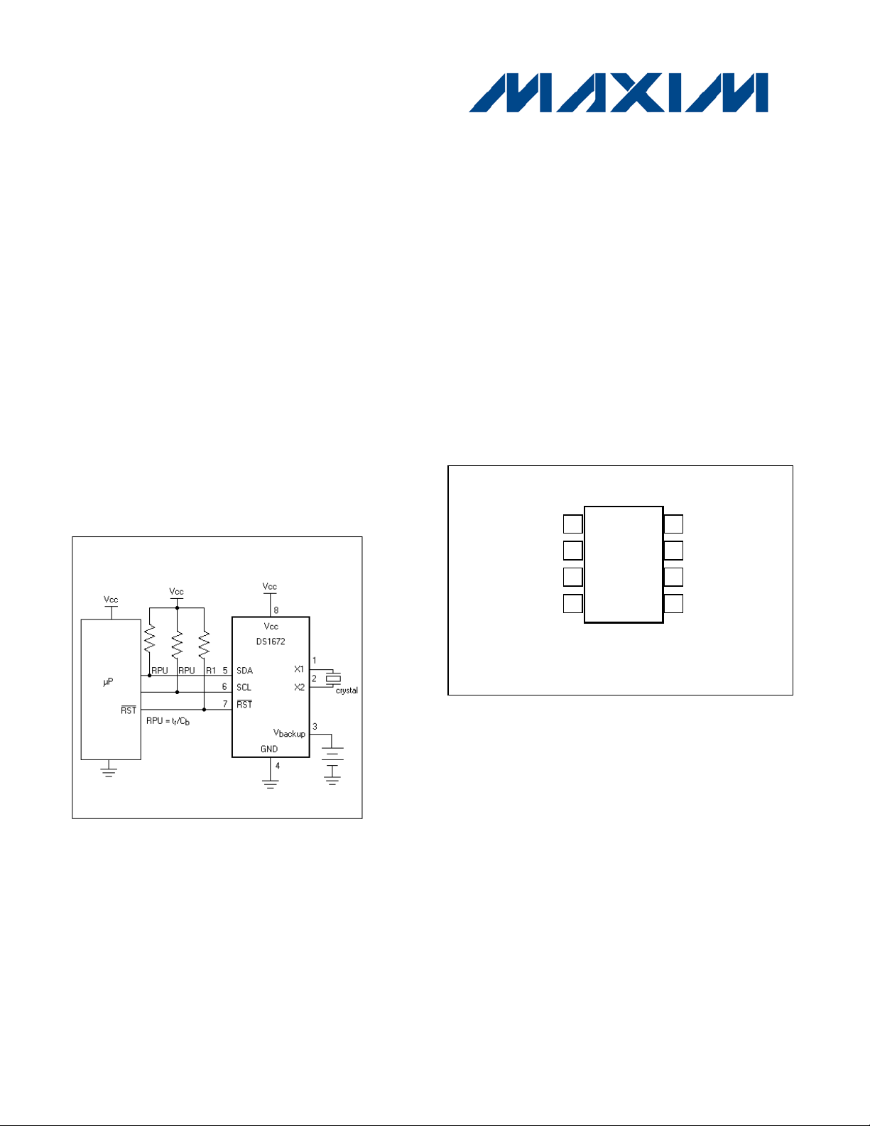
TYPICAL OPERATING CIRCUIT
PDIP
µ
TOP VIEW
1
2 3 4 8 7 6 5
VCC
RST
SCL
SDA
X1
X2
V
BACKUP
GND
DS1672
DS1672
I2C 32-Bit Binary Counter RTC
19-6032; Rev 9/11
GENERAL DESCRIPTION
The DS1672 incorporates a 32-bit counter and
power-monito ring funct ions. The 32-bit counter
is designed to count seconds and can be used to
derive time-of-day, week, month, month, and
year by using a software a lgorithm. A p re c is io n,
temperature-compensated reference and
comparator circuit monitors the status of VCC.
When an out-of-tolerance condition occurs, an
inte r na l powe r -fail signal is generated that for ces
the reset to the active stat e. When VCC r eturns to
an in-tolerance cond ition, the reset signal is kept
in the active state for a period of time to allow
the power supply and processor to stabilize.
FEATURES
32-Bit Counter
I2C Serial Interface
Automatic Power -Fail Detect and Switch
Circuitry
Power-Fail Res e t Output
Low-Voltage Oscillator Operat ion
(1.3V min)
Trickle-C harge Capability
Underwriters Labor at or ies (UL) Recog nized
-40°C to +85°C Operating Range
PIN CONFIGURATION
.
SO
SOP
1 of 15
Page 2

ORDERING INFORMATION
8 SO (150 mils)/Tape
and Reel
8 SO (150 mils)/Tape
and Reel
1672
rr -2
1672
rr -3
1672
rr -33
8 µSOP(3mm)/Tape
and Reel
1672
rr -33
PART TEMP RANGE VOLTAGE (V) PIN-PACKAGE TOP MARK*
DS1672-2+ -40°C to +85°C 2.0 8 PDIP (300 mils) DS1672-2
DS1672-3+ -40°C to +85°C 3.0 8 PDIP (300 mils) DS1672-3
DS1672-33+ -40°C to +85°C 3.3 8 PDIP (300 mils) DS1672-33
DS1672S-2+ -40°C to +85°C 2.0 8 SO (150 mils) D1672-2
DS1672S-3+ -40°C to +85°C 3.0 8 SO (150 mils) D1672-3
DS1672S-33+ -40°C to +85°C 3.3 8 SO (150 mils) D167233
DS1672
DS1672S-3+T&R -40°C to +85°C 3.0
DS1672S-33+T&R -40°C to +85°C 3.3
DS1672U-2+ -40°C to +85°C 2.0
DS1672U-3+ -40°C to +85°C 3.0
DS1672U-33+ -40°C to +85°C 3.3
8 µSOP(3mm)
8 µSOP(3mm)
8 µSOP(3mm)
DS1672U-33+T&R -40°C to +85°C 3.3
+ Denotes a lead-free/RoHS-compliant de vice.
* A “+” anywh er e on the top mark deno t es a lea d-free device. rr = 2-digit alphanumeric revision code.
D1672-3
D167233
2 of 15
Page 3
DS1672
DS1672-2
VCC
1.8
2.0
5.5
DS1672-3
VCC
2.7
3.0
5.5
DS1672-33
VCC
2.97
3.3
5.5
Logic 1
VIH
0.7 x VCC
V
CC
+ 0.5
V
Logic 0
VIL
-0.5
+0.3 x VCC
V
Backup Supply Voltage
V
BACKUP
1.3
3.0
3.63
V
PARAMETER
SYMBOL
CONDITIONS
MIN
TYP
MAX
UNITS
Active Supply Current
I
-2: VCC = 2.2V
600
µA
-3: VCC = 3.3V
-33: VCC = 3.63V
Standby C urrent
I
-2: VCC = 2.2V
500
µA
-3: VCC = 3.3V
-33: VCC = 3.63V
Power-F ail Vo ltage
VPF
-2:
2.70
2.88
2.97
V
-3:
2.45
2.60
2.70
-33:
1.58
1.70
1.80
V
BACKUP
L eakage Curre n t
I
BACKUPLKG
25
50
nA
Logic 0 Output (Note 4)
IOL
VOL = 0.4V
3
mA
Logic 0 Output (Note 4,
IOL
VCC > 2 V; VOL = 0.4V
3
mA
VCC < 2 V; VOL = VCC
* 0.2
ABSOLUTE MAXIMUM RATINGS
Voltage Range on Any Pin Relat ive to Ground……………………………………………..-0.5V to +6.0V
Operating Temperature Range (noncondensing) ...…………………………………………-40°C to +85°C
Storage Temperature Range……………………………………………………………….-55°C to +125°C
Soldering Temperature (reflow)………………………………………….…………………. +260°C
Lead Temperature (soldering, 10s) ……………………………………………………………….. +260°C
This is a stress rating only and functional operation of the device at these or any other conditions beyond those indicated in the operation
sections of this specification is not implied. Exposure to absolute maximum rating conditions for extended periods of time can affect device
reliability.
RECOMMENDED OPERATING CONDITIONS
(TA = -40°C to +85°C) (Note 1)
PARAMETER SYMBOL MIN TYP MAX UNITS
Supply
Voltage
Note 1: All voltages referenced to ground.
DC ELECTRICAL CHARACTERISTICS
(V
(Note 2)
(Note 3)
CCMIN
< VCC < V
CCMAX, TA
= -40°C to +85°C.) (Note 1)
CCA
CCS
V
DS1672-2 Onl y)
Note 1: All voltages referenced to ground.
Note 2: I
Note 3: I
Note 4: SDA and RST.
specified with SCL clocking at max frequency (400kHz), trickle charger disabled.
CCA
specified with VCC = V
CCS
and SDA, SCL = V
CCTYP
, tr ickle charger disabled.
CCTYP
3 of 15
Page 4
DC ELECTRICAL CHARACTERISTICS
V
BACKUP
Cu rrent (Oscillator On)
I
BACKUPOSC
0.425
1
µA
V
BACKUP
Current (Oscillator Off)
I
BACKUP
200
nA
Nomi nal Frequency
fO
32.768
kHz
Series Resistanc e
ESR
45
kΩ
Load Capacitance
CL 6 pF
(VCC = 0V, TA = -40°C to +85°C.) (Note 5)
PARAMETER SYMBOL MIN TYP MAX UNITS
Note 5: Using the recommended crystal on X1 and X2.
CRYSTAL SPECIFICATIONS
PARAMETER SYMBOL MIN TYP MAX UNITS
*The crystal, traces, and crystal input pins should be isolated from RF generating signals. Refer to Application Note 58: Crystal
Considerations for Dallas Real -Time Clocks for additional specifications
*
DS1672
4 of 15
Page 5

AC ELECTRICAL CHARACTERISTICS
Bus Free T ime
START Condition
Hold Time
Condition (Note 6 )
Fast mode
1.3
Setup Time for a
Condition
Rise T ime of B oth
Signals (Note 10)
Fall Time of Both
Signals (Note 10)
Ca pacitive Load for
(Note 10)
(VCC = 0V, TA = -40°C to +85°C.)
PARAMETER SYMBOL CONDITIONS MIN TYP MAX UNITS
DS1672
SCL Clock
Frequency
Bet ween a STOP a nd
(R epeated) STA RT
LOW Peri od of SCL
Clock
HIGH Period of SCL
Clock
Repea ted ST ART
Data Hol d Time
(Notes 7, 8)
Data Setup Time
(Note 9)
f
SCL
t
BUF
t
HD:STA
t
LOW
t
HIGH
t
SU:STA
t
HD:DAT
t
SU:DAT
Fast mode 100 400
Standard mod e 100
Fast mode 1.3
Standard mod e 4.7
Fast mode 0.6
Standard mod e 4.0
Standard mod e 4.7
Fast mode 0.6
Standard mod e 4.0
Fast mode 0.6
Standard mod e 4.7
Fast mode 0 0.9
Standard mod e 0
Fast mode 100
Standard mod e 250
kHz
µs
µs
µs
µs
µs
µs
ns
Fast mode 20 + 0.1CB 300
SDA and SC L
SDA and SC L
t
tF
R
Standard mod e 1000
Fast mode 20 + 0.1C
300
B
Standard mod e 300
Setup Time for STOP
Condition
Each Bus Line
I/O Capacitance C
Note 6: After this period, the first clock pulse is generated.
Note 7: A device must internally provide a hold time of at least 300ns for the SDA signal (referenced to the V
order to br i dge the undefined r egion of the fallin g edge of SC L.
Note 8:The maximum t
Note 9: A fast-mode device can be used in a standard-mode system, but the requirement t
automatically be the case if the device does not stretch the LOW period of the SCL signal. If such a device does stretch the LOW
period of the SCL signal, it must output the next data bit to the SDA line t
line is relea sed.
Note 10: C
–Total capacitance of one bus line in pF.
B
HD:DAT
t
SU:STO
CB 400 pF
I/O
has only to be met if the device does not stretch the LOW period (t
Fast mode 0.6
Standard mod e 4.0
10 pF
) of th e SCL sign al.
LOW
≥ to 250ns must then be met. This will
SU:DAT
m ax + t
R
= 1000 + 250 = 1250ns before the SCL
SU:DAT
ns
ns
µs
of the SCL signal) in
IHMIN
5 of 15
Page 6

POWER-UP/POWER-DOWN CHARACTERISTICS
VCC Detec t to RST (VCC Rising)
(Note 11)
SCL
START
SDA
STOP
t
BUF
REPEATED
START
t
HD:STA
t
LOW
t
HD:STA
t
HD:DAT
t
SU:DAT
t
HIGH
t
SU:STA
t
F
t
SU:STO
OUTPUTS
VCC
V
PF(max)
INPUTS
HIGH IMPEDANCE
RST
DON'T CARE
VALID
RECOGNIZED
RECOGNIZED
VALID
t
RPD
V
PF(min)
tF
tPD
tR
t
RPU
(TA = -40°C to +85°C)
PARAMETER SYMBOL MIN TYP MAX UNITS
DS1672
VCC Detec t to RST (VCC Falling) t
VCC Fa ll Time; V
PF(MAX)
VCC Ri se Tim e; V
Note 11: If the EOSC bit in the control register is set to logic 1, t
PF(MIN)
to V
to V
tF 300
PF(MIN)
tR 0
PF(MAX)
10 µs
RPD
t
250 ms
RPU
is equal to 250ms plus the startup time of the crystal oscillator.
RPU
µs
µs
Warning: Negative undershoots below –0.3V while the part is in battery-backed mode can cause
loss of data.
Figure 1. Ti m i ng Dia gr am
Figure 2. Power-Up/Power-Down Timing
6 of 15
Page 7

PIN DESCRIPTION
Connections for Standard 32.768kHz Quartz Crystal. The internal oscillator
co nnected to the exte rnal oscillator s igna l and t he X2 p in is left uncon nect ed.
Battery Input for Any Standard 3V L ithiu m Cel l or Ot her E nergy Source.
of Acceptability” at www.maxim-ic.com/qa/info/ul.
Serial-Data Input/O utput. SDA is the input/out put pin for the I2C s er ial
interface. The SDA pin is open dra in and requires an external pullup resistor.
I2C Serial-Clock Input. SCL is used to synchronize data movement on the
serial interface and requ ires an ext er nal pullup r es i stor.
Active-Lo w Reset Output. It functions as a micro processor reset signal. This
Power pin for Primary Po w er Supply. W hen VCC is applie d with in no rmal
VCC is belo w VPF, reads and writes are inhibited.
Figure 3. Recommended Layout for Crystal
LOCAL GROUND PLANE (LAYER 2)
CRYSTAL
X1
X2
GND
PIN NAME FUNCTION
circuitry is designed for operation with a crystal having a specified load
capacitance (CL) o f 6pF. For more information about crysta l select ion and
1, 2 X1, X2
crystal layout considerations, refer to Application Note 58: Crystal
Considerations with Dallas Real-Time Clocks. The DS1672 can also be driven
by an external 32.768kHz oscillator. In this configuration, the X1 pin is
Battery voltage must be held between 1.3V and 3.63V for proper operation.
Diodes placed in series between t he power source and the V
3 V
BACKUP
result in improper operation. If a backup supply is not required, V
be grounded. UL recognized to ensure against reverse charging curr ent whe n
used in conjunct ion with a lithium battery (charger disabled). S ee “Cond it io ns
4 GND Ground.
5 SDA
BACKUP
DS1672
pin ma y
BACKUP
must
6 SCL
7 RST
8 VCC
pin is an open-drain output and requires an external pullup resistor.
limits, the device is fully access ib le and dat a can b e wr itten and read. When
7 of 15
Page 8

DS1672
PARAMETER
SYMBOL
MIN
TYP
MAX
UNITS
NOTES
Nominal Frequency
FO
32.768
kHz
Series Resistance
ESR
45
kΩ
Load Capacitance
CL 6 pF
32-Bit Counter
(4 Bytes)
I2C Interface
Power Control
Address Register
Control Logic
1Hz
V
CC
V
BACKUP
GND
SCL
SDA
Control
Trickle Charger
X1 X2
RST
Dallas
Semiconductor
DS1672
C
L
C
L
N
Oscillator
and
divider
Detailed Description
The DS1672 provides a 32-bit co unter that inc reme nts onc e-per-second. The counter data is accessible
via an I2C serial interface. A precision, temperature-compensated, voltage reference and comparator
cir cu it mo nit or s VCC. Whe n VCC drops below VPF, RST becomes act ive and the interface is d isa bled t o
prevent data corruption. The device switches to the backup supply input, which maintains oscillator and
counter operation while VCC is absent . When VCC r ises above VPF, RST remains low for a period of time
(t
) to allow VCC to stabilize.
RPU
The block diagram in Figure 4 shows the main elements of the DS1672. As shown, communications to
and from the DS1672 occur ser ially o ver a I2C, bid irect ional bus. T he DS1672 o perat es as a s lave dev ice
on the I2C bus. Access is obtained by implementing a START condition and providing a device
identificat ion code fo llowed by a register add ress. Subseque nt reg isters can be accessed seque nt ially unt il
a STOP condition is executed.
Figure 4. Block Diagram
Oscillator Circuit
The DS1672 uses an external 32.768kHz crysta l. The oscillator circu it does not require any external
resistors or capac itor s to o per at e. Table 1 specifies severa l cr yst al parameters for the external crysta l.
Figure 4 shows a functional sc hematic of the oscillator circuit. If using a cr ystal with the specif ied
characterist ics, the startup time is usually less than one second.
Table 1. Crystal Specifications*
* The crystal, traces, and crystal input pins should be isolated from RF gen erating signals. Refer to Application Note 58:
Clock Accur acy
The accuracy o f the clock is dependent upon the accuracy o f the crystal and the accurac y of the match
between the capacitive load of the oscillator circuit and the capacitive load for which the crystal was
8 of 15
Page 9

DS1672
ADDRESS
B7
B6
B5
B4
B3
B2
B1
B0
FUNCTION
00h
LSB
Counter Byte 1
01h
Counter Byte 2
02h
Counter Byte 3
03h
MSB Counter Byte 4
04h
EOSC
Control
05h
TCS
TCS
TCS
TCS
DS
DS
RS
RS
Trick le Ch arger
READ/WRITE
ACCESS
RST
VCC < VPF, VCC < V
BACKUP
No
Active
V
BACKUP
VCC < VPF, VCC > V
BACKUP
No
Active
VCC
VCC > VPF, VCC < V
BACKUP
Yes
Inactive
VCC
VCC > VPF, VCC > V
BACKUP
Yes
Inactive
VCC
trimmed. Additional error will be added by crystal frequency drift caused by temperature shifts. External
circuit noise coup led into the oscillator circuit may result in the clock running fast . Refer to Application
Note 5: “Crystal Considerations with Dallas Real-Time Clocks” for detailed information.
Address Map
The counter is accessed by reading or writing the first 4 bytes of the DS1672 (00h–03h) . The co ntrol
register and t rick le charger are ac cessed by r eadin g o r writ ing the appr op riate r egister b ytes as illustr at ed
in Table 2. If the master co ntinues to send or request more d ata after the address pointer has reached 05h,
the address pointer w ill wrap aro und to location 00h.
Table 2. Reg isters
Power Control
The device is fully accessible and data can be written and ready only when VCC is greater than VPF.
Ho weve r, whe n VCC falls below VPF, (point at which write prot ection occurs) t he internal clock reg ister s
are blocked from any access. If VPF is less than V
V
BACKUP
VCC to V
the V
wh en VCC drops below VPF. I f VPF is great er than V
BACKUP
BACKUP
w hen VCC drops below V
BACKUP
so u rce u ntil VCC is r etu rned to nominal levels (see Table 3).
. Oscillato r and counter operation a re maint ained fro m
BACKUP
, the device power is switched from VCC to
BACKUP
, the device power is switched from
Table 3. Power Control
SUPPLY CONDITION
POWERED BY
Oscillator Control
The EOSC b it ( bit 7 o f the contro l register) co ntrols the osc illator when in back-up mode. This bit when
set to log ic 0 will st art the oscillator . When this bit is set to a logic 1, the oscillator is stopped and the
DS1672 is placed into a low-power standby mode (I
powered by V
the oscil lat o r is alwa ys on regardless of the stat us of the EOSC bit ; ho w e ver, the counter
CC,
BACKUP
) whe n in ba ck-up mode. When the DS1672 is
is incremented only when EOSC is a logic 0.
Microprocessor Monitor
A temperature-compensated comparator circuit monitors the level of VCC. Whe n VCC fa lls to the p owe rfail trip point, the RST signal (open drain) is pulled active, and read/write access is inhibited. When VCC
ret ur ns to no minal le ve ls , the RST signal is k ept in the active state for t
supply and microp rocessor to st abilize. Note, however, t hat if the EOSC bit is set to a logic 1 (to disable
the o scillator during write protection), the reset signal will be kept in an active state for t
startup time of the oscillator.
(typically) to allow the power
RPU
plus the
RPU
9 of 15
Page 10

DS1672
X X X X 0 0 X X Disabled
X X X X 1 1 X X Disabled
X X X X X X 0 0 Disabled
1 0 1 0 0 1 0
1
No diode, 250Ω resistor
1 0 1 0 1 0 0
1
One diode, 250Ω resistor
1 0 1 0 0 1 1
0
No diode, 2kΩ resistor
1 0 1 0 1 0 1
0
One diode, 2kΩ resistor
1 0 1 0 0 1 1
1
No diode, 4kΩ resistor
1 0 1 0 1 0 1
1
One diode, 4kΩ resistor
0 0 0 0 0 0 0 0 Initial defa ult va lue--disabled
Trickle Charger
The trickle charger is controlled by the trickle charge register. The simplified schematic of Figure 5
shows the basic components o f the t r ickle charger. T he tr ickle c harge se lect (T CS) b it (bits 4–7) co nt rols
the select ion of the t rickle charger. In order to prevent accidenta l enabling, only a patt ern on 1010 will
enable the tr ickle charger. Al l ot her patt erns will disable the trickle charger. The DS1672 powers up with
the trickle charger disabled. The diode select (DS) bits (bits 2, 3) select whether or not a diode is
connected between VCC and V
BACKUP
The RS bits (bits 0, 1 ) se lect whet her a resistor is connected bet ween VCC and V
of the resistor is. The resist or selected by the resisto r select (RS) bits and the diode select ed by the diode
select (DS) bits are as follows:
TCS TCS TCS TCS DS DS RS RS FUNCTION
. If DS is 01, no diode is selected o r if DS is 10, a diode is select ed.
BACKUP
and what the value
Warning: The resistor value of 250Ω must not be selected whenever V
is greater
CC
than 3.63V.
Diode and resisto r se lect ion is deter mined by the user according to the maximum current des ired for
battery or super cap charg ing. The maximum c harging current can be calculated as illustrated in the
following exa mple. Assume t ha t a syste m power supply of 3V is applied to VCC and a super cap is
connected to V
bet ween V
and V
CC
BACKUP
As the super cap changes, the vo ltage drop between VCC and V
charge current w ill decrease.
. Also assume that the trickle charger has been e nabled with a diode and resistor R2
BACKUP
. T he maximum current I
I
= (5.0V - diode drop) / R1 ≈ (5.0V - 0.6V) / 2kΩ ≈ 2.2mA
MAX
would, t herefore, be ca lculated as follows:
MAX
BACKUP
will decrease and, therefore, the
10 of 15
Page 11

DS1672
1 OF 16 SELECT
NOTE: ONLY 1010 ENABLES
1 OF 2
SELECT
1 OF 3
SELECT
TCS
TCS
TCS
TCS
DS
DS
RS
RS
BIT 7
BIT 6
BIT 5
BIT 4
BIT 3
BIT 2
BIT 1
BIT 0
250Ω
R1
R2
TRICKLE CHARGE REGISTER
TCS =
TRICKLE CHARGER SELECT
DS =
DIODE SELECT
RS =
RESISTOR SELECT
VCC
V
2kΩ
R3
4k
Figure 5. Programmable Trickle Charger
BACKUP
Ω
2
I
C Serial Data Bus
The DS1672 supports a bidirectional I2C bus and data transmission proto col. A device that sends dat a
onto the bus is de fined as a tr ansmitt er and a devi ce rece iving dat a as a rece iver. T he device that contr ols
the message is c a lled a master. The de vices t hat are co ntro lled by t he mast er are s laves. T he bus must be
controlled by a master device that generates t he se rial clock (SCL), controls the bus a ccess, and ge nerates
the START and STOP conditions. The DS1672 operates as a s lave on the I2C bus. Connections to the bus
are made via the open-drain I/O lines SDA and SCL. Within the bus specifications, a standard mode
(100kHz maximum clock rate) and a fast mode (400kHz maximum clock rate) are defined. The DS1672
op erat es in bo th mo des.
The fo llo w in g bus protocol has been defined (Figure 6):
Data transfe r may be initiated only w hen the bus is not busy.
During data tr ansfer, the dat a line must r emain stable whenever the clock line is HIGH. Changes i n
the dat a lin e whi le the clock line is high will be interpret ed as contro l signals.
Accordingly, the follow ing bus condition s have been defined:
Bus not busy: Both data and clock lines remain HIGH.
Start data transfer: A change in the state of the data line fro m high to low, while the clock line is
high, defines a START condit ion.
Stop data transfer: A change in the state o f the data line from low t o high, while the clock line i s
high, defines a STOP condition.
11 of 15
Page 12

DS1672
Data valid: The st ate of the data l ine represents valid dat a when, after a ST ART condition, the
data line is stable for t he duration o f the high perio d of the clock signal. T he data o n the line must
be changed during the low period of the clock signal. There is one clock pulse per bit o f data.
Each data transfer is initiated with a START condition and terminated with a STOP condition.
The number of data bytes transferred between the START a nd t he ST OP conditions is not limited,
and is determined by the master device. The information is transferred byte-wise and each
receiver acknowledges with a ninth bit. Within the I2C bus specifications a standard mode
(100kHz clock rate) and a fast mode (400kHz clock rate) are defined.
Acknowledge: Each receiving device, when addressed, is obliged to generate an acknowledge
after the reception of each byte. The master device must generate an extra clock pulse that is
associated with th is acknow ledge bit.
A device that acknowledges must pull do wn the SDA line during the acknowledge clock pulse in
such a way that t he SDA line is stab le LOW during t he HIGH period o f the acknow ledge related
clock pulse. O f co urse, setup and ho ld t imes must be t aken into acco unt. A mast er must signa l an
end of data to the slave by not generating an acknowledge bit on the last byte that has been
clocked out of the slave. In this case, the slave must leave the dat a line HIGH to enable t he master
to generate the STOP co nd ition.
Figures 7 and 8 detail how data tr ansfer is acco mplished on the I2C bus. Depending upon the state of the
R/W bit, two types of data t r ansfer are possible:
1) Data transfer from a master transmitter to a slave receiver. The first byte transmitted by the
master is the s lave address. Ne xt follows a number of data bytes. The slave ret urns an acknow ledge
bit after each received byte.
2) Data transfer from a slave transmitter to a master receive r. The first byte (the slave addr ess) is
transmitted by t he master. T he slave then retur ns an acknowledge bit. Next fo llows a number of data
bytes transmitted b y the slave to the master . The master ret urns an acknowledge bit after all received
bytes other than the last byte. At t he end of the last rece ived byte, a “not acknowledge” is returned.
The master device generates all of the serial clock pulses and the START and STOP conditions. A
tr ansfer is e nded wit h a ST OP c ond itio n or with a repeat ed START condition. Since a rep eated START
co ndit ion is also the beginning of the next serial t ransfer, the bus will not be released.
The DS1672 can operate in the following two modes:
1) Slave receiver mode (DS1672 write mode): Serial data and clock are received through SDA and
SCL. After each byte is received, an acknowledge bit is t r ansmitted . S T ART and STOP conditions are
recognized as the beginning and end of a serial transfer. Address recognition is performed by
hardware after reception of the slave address and d irection bit (Figure 7). T he slave addr ess byte is t he
first byte received after the START condition is generated by the master. The slave address byte
contains the 7-bit DS1672 address, which is 1101000, followed by the direction bit (R/W), wh ich fo r
a write is a 0. After receiving and decoding the slave address byte the DS1672 outputs an
acknowledge on the SDA line. After the DS1672 acknowledges the slave address + write bit, the
master transmits a word address to the DS1672. This will set the register pointer o n the DS1672, wit h
the DS1672 ack nowledging t he transfer. T he master ma y then t ransmit zero or more bytes of data,
12 of 15
Page 13

DS1672
MSB
slave address
R/W
direction
bit
SDA
SCL
START
CONDITION
1 2 6 7 8 9
1 2 8 9
STOP CONDITION
OR
REPEATED
START CONDITION
3 - 8
acknowledgement
signal from receiver
acknowledgement
signal from receiver
ACK ACK
repeated if more bytes
are transferred
with the DS1672 acknowledging each byte received. The register pointer will increment after each
byte is transferred. The mast er will generate a stop condition to terminate the dat a wr ite.
2) Slave transmitter mode (DS1672 read mode): The first byte is rece ived and handled as in the slave
receiver mode. However, in this mode, the direction bit will indicate that the transfer direction is
reversed. Ser ia l data is t ransmitted o n SDA by the DS1 672 while the serial clock is input on SCL.
START and STOP co nditions are recognized as t he beginning and e nd of a serial transfer (Figure 8) .
The slave address byte is t he first byte received after the START condition is generated by the master.
The slave address byte contains the 7-bit DS1672 address, which is 1101000, followed by the
d ire ct io n bit ( R/ W), which for a read is a 1. After rece iving and decod ing the slave address byte the
DS1672 outputs an acknowledge on the SDA line. The DS1672 then begins to transmit data starting
with the register address pointed to by the register pointer. If the register pointer is not written to
before the init iation of a read mode the first add ress that is read is the last o ne stored in the reg ister
pointer. The DS1672 must r eceive a “not ackno wledge” to end a read.
Figure 6. Data Transfer on I2C Serial Bus
Figure 7. Data Write: Slave Receiver Mode
<Slave Address> <Word Address (n)> <Data(n) <Data(n+1)> <Data(n+X)>
<RW>
AXXXXXXXXA1101000S 0 XXXXXXXX A XXXXXXXX A XXXXXXXX A P
S - START
A - ACKNOWLEDGE
P - STOP
R/W - READ/WRITE O R DI RECTION BIT ADDRESS = D0H
DATA TRANSFERRED
(X+1 BYTES + ACKNOWLEDGE)
13 of 15
Page 14

DS1672
PACKAGE
THETA-JA
THETA-JC
8 PDIP (300 mi ls )
110°C/W
40°C/W
8 SO (150 mils)
128.4°C/W
36°C/W
8 µSOP (3mm)
206.3°C/W
42°C/W
8 PDIP (300 mi ls )
P8+1
21-0043
—
8 SO (150 mils)
S8+5
21-0041
90-0096
8 µSOP (3mm)
U8+1
21-0036
90-0092
Figure 8. Data Read: Slave Transmitter Mode
<Slave Address> <Data(n)> <Data(n+1) <Data(n+2)> <Data(n+X)>
S - START
A - ACKNOWLEDGE
P - STOP
A - NOT ACKNOWLEDGE
R/W - READ/WRITE O R DI RECTION BIT ADDRESS = D1H
<RW>
AXXXXXXXXA1101000S 1 XXXXXXXX A XXXXXXXX A XXXXXXXX A P
(X+1 BYTES + ACKNOWLEDGE); NOTE: LAST DATA BYTE IS
FOLLOWED BY A NOT ACKNO WLEDGE (A) SIGNAL)
DATA TRANSFERRED
THERMAL INFORMATION
PACKAGE INFORMATION
For the latest package outline inf ormation and land patterns (footprints), go to www.maxim-ic.com/packages. Note
that a “+”, “#”, or “-“ in the package code i ndic ates RoHS status only. Package drawings may show a different suffix
character, but t he dr awing per tains to the package regardless of RoHS status.
PACKAGE TYPE PACK AGE CODE OUTLIN E N O . LAND PATTERN NO.
14 of 15
Page 15

REVISION HISTORY
REVISION
DATE
PAGES
CHANGED
Updated the Ordering Information, Absolute Maximum Ratings,
Information, and Package Information
DS1672
DESCRIPTION
9/11
Recommended Operating Conditions, DC Electrical Characteristics, AC
Electrical Characteristics, Pin Description, Trickle Charger, Thermal
2, 3, 5, 7,
10, 15
15 of 15
Maxim cannot assume responsibility for use of any circuitry other than circuitry entirely embodied in a Maxim product. No circuit patent licenses are implied. Maxim
reserves the right to change the circuitry and specifications without notice at any time.
Maxim Integrated Products, 120 San Gabriel Drive, Sunnyvale, CA 94086 408-737-7600
© 2011 Maxim Integrated Products Maxim is a registered tr ademark of Ma xi m I nt egrated Pr oduc ts , Inc .
 Loading...