

Page 1
DS1340
I2C RTC with Trickle Charger
________________________________________________________________
Maxim Integrated Products
1
For pricing, delivery, and ordering information, please contact Maxim Direct at 1-888-629-4642,
or visit Maxim’s website at www.maxim-ic.com.
General Description
The DS1340 is a real-time clock (RTC)/calendar that is
pin compatible and functionally equivalent to the ST
M41T00, including the software clock calibration. The
device additionally provides trickle-charge capability
on the V
BACKUP
pin, a lower timekeeping voltage, and
an oscillator STOP flag. Block access of the register
map is identical to the ST device. Two additional registers, which are accessed individually, are required for
the trickle charger and flag. The clock/calendar provides seconds, minutes, hours, day, date, month, and
year information. A built-in power-sense circuit detects
power failures and automatically switches to the backup supply. Reads and writes are inhibited while the
clock continues to run. The device is programmed serially through an I2C bidirectional bus.
Applications
Portable Instruments
Point-of-Sale Equipment
Medical Equipment
Telecommunications
Features
♦ Enhanced Second Source for the ST M41T00
♦ Available in a Surface-Mount Package with an
Integrated Crystal (DS1340C)
♦ Fast (400kHz) I2C Interface
♦ Software Clock Calibration
♦ RTC Counts Seconds, Minutes, Hours, Day, Date,
Month, and Year
♦ Automatic Power-Fail Detect and Switch Circuitry
♦ Trickle-Charge Capability
♦ Low Timekeeping Voltage Down to 1.3V
♦ Three Operating Voltage Ranges (1.8V, 3V, and 3.3V)
♦ Oscillator Stop Flag
♦ Available in 8-Pin µSOP or SO Packages
♦ Underwriters Laboratories (UL) Recognized
Ordering Information
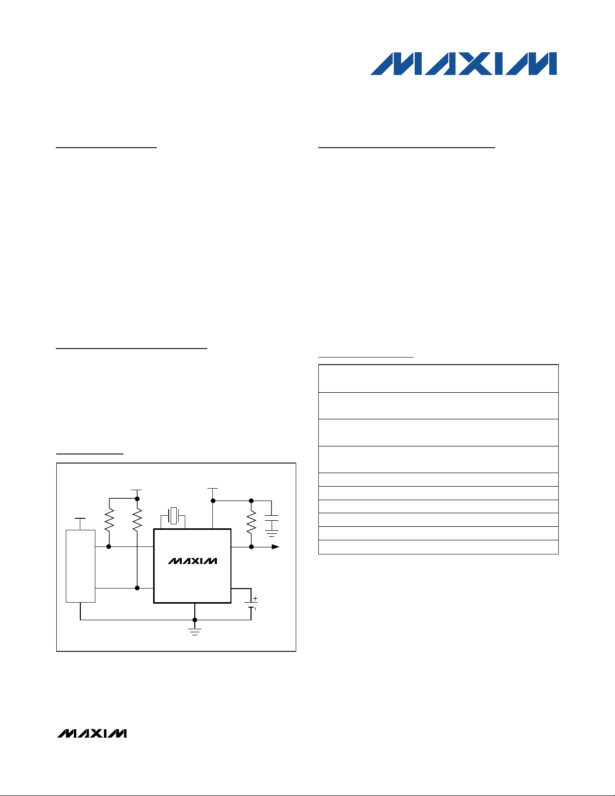
4
CPU
V
CC
V
CC
V
CC
5
6
8
12
SDA
SCL
GND
X2X1
V
CC
C1
R
PU
R
PU
CRYSTAL
FT/OUT
V
BACKUP
3
7
R
PU
= tR / CB
DS1340
Typical Operating Circuit
PART TEMP RANGE
PINPACKAGE
TOP MARK
†
DS1340Z-18+ -40°C to +85°C
8 SO
(0.150in)
D1340-18
DS1340Z-3+ -40°C to +85°C
8 SO
(0.150in)
DS1340-3
DS1340Z-33+ -40°C to +85°C
8 SO
(0.150in)
D134033
DS1340U-18+ -40°C to +85°C 8 μSOP 1340 -18
DS1340U-3+ -40°C to +85°C 8 μSOP 1340 -3
DS1340U-33+ -40°C to +85°C 8 μSOP 1340 -33
DS1340C-18# -40°C to +85°C 16 SO DS1340C-18
DS1340C-3# -40°C to +85°C 16 SO DS1340C-3
DS1340C-33# -40°C to +85°C 16 SO DS1340C-33
Pin Configurations appear at end of data sheet.
+
Denotes a lead(Pb)-free/RoHS-compliant package.
#
Denotes a RoHS-compliant device that may include lead(Pb)
that is exempt under RoHS requirements. The lead finish is
JESD97 category e3, and is compatible with both lead-based
and lead-free soldering processes.
†
A "+" anywhere on the top mark denotes a lead(Pb)-free device.
A "#" denotes a RoHS-compliant device.
19-5578; Rev 7; 8/11
Page 2
DS1340
I2C RTC with Trickle Charger
2 _______________________________________________________________________________________
ABSOLUTE MAXIMUM RATINGS
RECOMMENDED DC OPERATING CONDITIONS
(VCC= V
CC MIN
to V
CC MAX
, TA= -40°C to +85°C, unless otherwise noted. Typical values are at VCC= 3.3V, TA= +25°C, unless
otherwise noted.) (Note 1)
Stresses beyond those listed under “Absolute Maximum Ratings” may cause permanent damage to the device. These are stress ratings only, and functional
operation of the device at these or any other conditions beyond those indicated in the operational sections of the specifications is not implied. Exposure to
absolute maximum rating conditions for extended periods may affect device reliability.
Voltage Range on VCCPin Relative to Ground .....-0.3V to +6.0V
Voltage Range on SDA, SCL, and FT/OUT
Relative to Ground..................................-0.3V to (V
CC
+ 0.3V)
Operating Temperature Range ...........................-40°C to +85°C
Storage Temperature Range .............................-55°C to +125°C
Lead Temperature (soldering, 10s) .................................+260°C
Soldering Temperature (reflow) .......................................+260°C
Supply Voltage (Note 2) V
Input Logic 1 (SDA, SCL) VIH (Note 2) 0.7 x VCC V
Input Logic 0 (SDA, SCL) VIL (Note 2) -0.3 +0.3 x VCC V
Supply Voltage, Pullup
(FT/OUT, SDA, SCL), V
Bac kup Supply Voltage (Note 2) V
Trickle-Charge Current-Limiting
Resistors
Power-Fail Voltage (Note 2) V
Input Leakage (SCL, CLK) ILI -1 +1 μA
I/O Leakage (SDA, FT/OUT) ILO -1 +1 μA
SDA Logic 0 Output I
FT/OUT Logic 0 Output I
Active Supply Current (Note 7) I
Standby Current (Note 8) I
V
BACKUP
PARAMETER SYMBOL CONDITIONS MIN TYP MAX UNITS
Lea kage Current I
DS1340-18 1.71 1.8 5.5
DS1340-3 2.7 3.0 5.5
DS1340-33 2.97 3.3 5.5
(Note 2) 5.5 V
DS1340-18 1.3 3.7
DS1340-3 1.3 3.7
DS1340-33 1.3 5.5
DS1340-18 1.51 1.6 1.71
DS1340-3 2.45 2.6 2.7
DS1340-33 2.70 2.88 2.97
VCC > 2V; VOL = 0.4V 3.0
1.7V < VCC < 2V; VOL = 0.2 x VCC 3.0
VCC > 2V; VOL = 0.4V 3.0
1.7V < VCC < 2V; VOL = 0.2 x VCC 3.0
1.3V < VCC < 1.7V; VOL = 0.2x VCC 250 μA
DS1340-18; VCC = 1.89V 72 150
DS1340-3; VCC = 3.3V 108 200
DS1340-33; VCC = 5.5V 192 300
DS1340-18; VCC = 1.89V 60 100
DS1340-3; VCC = 3.3V 81 125
DS1340-33; VCC = 5.5V 100 150
= 3.7V 100 nA
CC
= 0V
CC
V
PU
BACKUP
R1 (Notes 3, 4) 250
R2 (Note 5) 2000
R3 (Note 6) 4000
PF
OLSDA
OLSQW
CCA
CCS
BACKUPLKG VBACKUP
+ 0.3 V
CC
V
V
V
mA
mA
μA
μA
Page 3
DS1340
I2C RTC with Trickle Charger
_______________________________________________________________________________________ 3
DC ELECTRICAL CHARACTERISTICS
(VCC= 0V, V
BACKUP
= 3.7V, TA= -40°C to +85°C, unless otherwise noted.) (Note 1)
AC ELECTRICAL CHARACTERISTICS
(VCC= V
CC MIN
to V
CC MAX
, TA= -40°C to +85°C, unless otherwise noted.) (Notes 1,14, Figure 1)
V
BACKUP
V
BACKUP
PARAMETER SYMBOL CONDITIONS MIN TYP MAX UNITS
Current
Data-Retention Current I
I
BACKUP1
I
BACKUP2
I
BACKUP3
BACKUPDR
OSC ON, FT = 0 (Note 9) 800 1150
OSC ON, FT = 1 (Note 9) 850 1250
OSC ON, FT = 0, V
= +25°C (Notes 9, 10)
T
A
OSC OFF 25.0 100 nA
SCL Clock Frequenc y f
Bus Free Time Between STOP
and START Condition s
Hold Time (Repeated) START
Condition (Note 11)
Low Period of SCL Clock t
High Period of SCL Clock t
Data Hold Time (Notes 12, 13) t
Data Setup Time (Note 14) t
START Setup Time t
Rise T ime of SDA and SCL
Signals (Note 15)
Fall Time of SDA and SCL
Signals (Note 15)
Setup Time for STOP Condition t
Capacitive Load for Each Bus
Line
I/O Capacitance (SCL, SDA) C
Pulse Width of Spikes that Must
be Suppressed by the Input
Filter
Oscillator Stop Flag (OSF) Delay t
PARAMETER SYMBOL CONDITIONS MIN TYP MA X UNITS
SCL
t
BUF
t
HD: STA
LOW
HIGH
HD:DAT
SU:DAT
SU:STA
t
R
t
SU:STO
C
I/O
t
SP
OSF
Standard mode 0 100
Fast mode 100 400
Standard mode 4.7
Fast mode 1.3
Standard mode 4.0
Fast mode 0.6
Standard mode 4.7
Fast mode 1.3
Standard mode 4.0
Fast mode 0.6
Standard mode 0 0.9
Fast mode 0 0.9
Standard mode 250
Fast mode 100
Standard mode 4.7
Fast mode 0.6
Standard mode 20 + 0.1CB 1000
Fast mode 20 + 0.1CB 300
Standard mode 20 + 0.1CB 300
F
Fast mode 20 + 0.1CB 300
Standard mode 4.7
Fast mode 0.6
(Note 15) 400 pF
B
10 pF
Fast mode 30 ns
(Note 16) 100 ms
BACKUP
= 3.0V,
nA
800 1000
kHz
μs
μs
μs
μs
μs
ns
μs
ns
ns
μs
Page 4
DS1340
I2C RTC with Trickle Charger
4 _______________________________________________________________________________________
POWER-UP/POWER-DOWN CHARACTERISTICS
(TA= -40°C to +85°C) (Figure 2)
WARNING: Under no circumstances are negative undershoots, of any amplitude, allowed when device is in battery-backup mode.
Note 1: Limits at -40°C are guaranteed by design and not production tested.
Note 2: All voltages are referenced to ground.
Note 3: Measured at V
CC
= typ, V
BACKUP
= 0V, register 08h = A5h.
Note 4: The use of the 250Ω trickle-charge resistor is not allowed at V
CC
> 3.63V and should not be enabled.
Note 5: Measured at V
CC
= typ, V
BACKUP
= 0V, register 08h = A6h.
Note 6: Measured at V
CC
= typ, V
BACKUP
= 0V, register 08h = A7h.
Note 7: I
CCA
—SCL clocking at max frequency = 400kHz.
Note 8: Specified with I
2
C bus inactive.
Note 9: Measured with a 32.768kHz crystal attached to the X1 and X2 pins.
Note 10: Limits at +25°C are guaranteed by design and not production tested.
Note 11: After this period, the first clock pulse is generated.
Note 12: A device must internally provide a hold time of at least 300ns for the SDA signal (referred to as the V
IH(MIN)
of the SCL
signal) to bridge the undefined region of the falling edge of SCL.
Note 13: The maximum t
HD:DAT
only has to be met if the device does not stretch the low period (t
LOW
) of the SCL signal.
Note 14: A fast-mode device can be used in a standard-mode system, but the requirement t
SU:DAT
≥ to 250ns must be met. This
is automatically the case if the device does not stretch the low period of the SCL signal. If such a device does stretch the
low period of the SCL signal, it must output the next data bit to the SDA line t
R MAX
+ t
SU:DAT
= 1000 + 250 = 1250ns
before the SCL line is released.
Note 15: C
B
—total capacitance of one bus line in pF.
Note 16: The parameter t
OSF
is the period of time the oscillator must be stopped for the OSF flag to be set over the 0V ≤ VCC≤
V
CCMAX
and 1.3V ≤ V
BAT
≤ 3.7V range.
Note 17: This delay applies only if the oscillator is enabled and running. If the oscillator is disabled or stopped, no power-up delay
occurs.
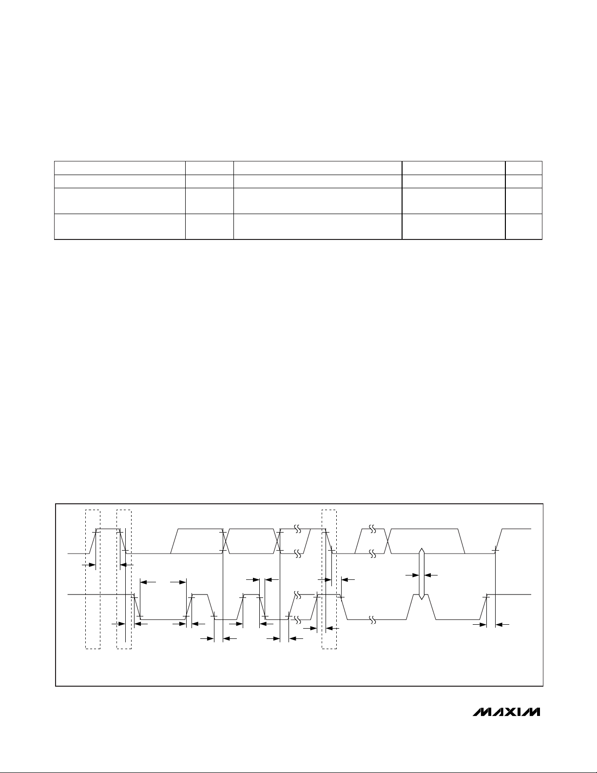
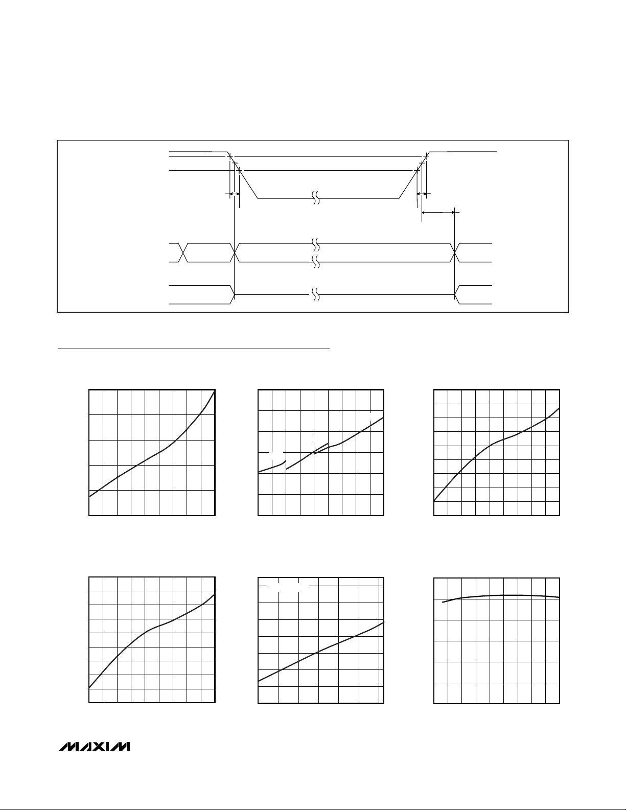
Figure 1. Data Transfer on I2C Serial Bus
Recovery at Power-Up t
VCC Fall Time; V
V
PF(MIN)
VCC Rise Time; V
V
PF(MAX)
PARAMETER SYMBOL CONDITIONS MIN TYP MAX UNITS
REC
PF(MIN)
to
to
t
VCCF
t
VCCR
PF(MAX)
(Note 17) 2 ms
300 µs
0µs
SDA
t
BUF
t
LOW
SCL
t
HD:STA
STOP START REPEATED
NOTE: TIMING IS REFERENCED TO V
IL(MAX)
AND V
IH(MIN)
t
R
t
HD:DAT
.
t
HIGH
t
F
t
SU:DAT
START
t
SU:STA
t
HD:STA
t
SP
t
SU:STO
Page 5
DS1340
I2C RTC with Trickle Charger
_______________________________________________________________________________________ 5
Figure 2. Power-Up/Power-Down Timing
Typical Operating Characteristics
(VCC= +3.3V, TA= +25°C, unless otherwise noted.)
I
CCSA
vs. VCC FT = 0
DS1340 toc01
VCC (V)
SUPPLY CURRENT (μA)
5.04.54.03.53.02.52.01.5
50
100
150
200
250
0
1.0 5.5
25
50
75
100
125
150
0
I
CCS
vs. VCC FT = 0
DS1340 toc02
VCC (V)
SUPPLY CURRENT (μA)
5.04.54.03.53.02.52.01.51.0 5.5
-1.8V
-3.0V
-3.3V
I
BACKUP1
(FT = 0) vs. V
BACKUP
DS1340 toc03
450
500
550
600
650
700
750
800
850
400
V
BACKUP
(V)
SUPPLY CURRENT (nA)
5.04.54.03.53.02.52.01.51.0 5.5
I
BACKUP2
(FT = 1) vs. V
BACKUP
DS1340 toc04
450
500
550
600
650
700
750
800
850
400
V
BACKUP
(V)
SUPPLY CURRENT (nA)
5.04.54.03.53.02.52.01.51.0 5.5
I
BACKUP3
vs. TEMPERATURE
DS1340 toc05
TEMPERATURE (°C)
SUPPLY CURRENT (nA)
6040-20 0 20
500
550
600
650
700
750
800
850
-40 80
V
BACKUP
= 3.0V
OSCILLATOR FREQUENCY vs. SUPPLY VOLTAGE
(FT x 64)
DS1340 toc06
V
BACKUP
(V)
FREQUENCY (Hz)
5.04.54.03.53.02.52.01.5
32768.1
32768.2
32768.3
32768.4
32768.5
32768.6
32768.0
1.0 5.5
V
CC
V
V
INPUTS
OUTPUTS
PF(MAX)
PF(MIN)
RECOGNIZED RECOGNIZED
VALID
V
t
F
PF
DON'T CARE
HIGH-Z
V
PF
t
R
t
REC
VALID
Page 6

DS1340
I2C RTC with Trickle Charger
6 _______________________________________________________________________________________
Detailed Description
The DS1340 is a low-power clock/calendar with a trickle
charger. Address and data are transferred serially
through a I2C bidirectional bus. The clock/calendar provides seconds, minutes, hours, day, date, month, and
year information. The date at the end of the month is
automatically adjusted for months with fewer than 31
days, including corrections for leap year. The DS1340
has a built-in power-sense circuit that detects power failures and automatically switches to the backup supply.
Power Control
The power-control function is provided by a precise,
temperature-compensated voltage reference and a
comparator circuit that monitors the VCClevel. The
device is fully accessible and data can be written and
read when VCCis greater than VPF. However, when V
CC
falls below VPF, the internal clock registers are blocked
from any access. If V
PF
is less than V
BACKUP
, the
device power is switched from VCCto V
BACKUP
when
VCCdrops below VPF. If VPFis greater than V
BACKUP
,
the device power is switched from VCCto V
BACKUP
Pin Description
Table 1. Power Control
PIN
816
1 — X1
2 — X2
3 14 V
4 15 GND Ground
5 16 SDA
6 1 SCL
7 2 FT/OUT
8 3 V
— 4–13 N.C. No Connection. Mu st be connected to ground.
NAME FUNCTION
Connections for a Standard 32.768kHz Quartz Crystal. The internal oscillator circuitry is designed for
operation with a crystal having a specified load capacitance (C
oscillator and can optionally be connected to an external 32.768kHz oscillator. The output of the
internal oscillator, X2, is left unconnected if an external oscillator is connected to X1.
Connect ion for a Secondary Power Supply. For the 1.8V and 3V dev ices, V
between 1.3V and 3.7V for proper operation. D iodes p laced in series between the supply and the input
BACKUP
CC
pin may result in improper operation. V
This pin can be connected to a primary cell such as a lithium coin cell. Additionally, this pin can be
connected to a rechargeable cell or a super cap when used with the trickle-charge feature. UL recognized to
ensure against reverse charging when used with a lithium battery (www.maxim-ic.com/qa/info/ul).
Serial Data Input/Output. SDA is the data input/output for the I
drain and requires an e xternal pullup resistor.
Serial Clock Input. SCL is the clock input for the I
movement on the serial interface.
Frequency Test/Output. This pin is u sed to output either a 512H z signal or the va lue of the OUT bit.
When the FT bit is logic 1, the FT/OUT pin toggles at a 512Hz rate. When the FT bit i s logic 0, the
FT/OUT pin reflects the value of the OUT bit. This open-drain pin requires an external pullup resistor,
and operates with e ither V
the voltage on V
Primary Power Supply. When vo ltage is applied within normal limits, the device is fully accessib le and
data can be written and read. When a backup supply is connected to the device and V
reads and writes are inhibited. However, the timekeeping function continues unaffected by the lower
input voltage.
. If not used, this pin can be left unconnected.
CC
CC
or V
BACKUP
applied. The pul lup vo ltage can be up to 5.5V, regardless of
BACKUP
) of 12.5pF. X1 is the input to the
L
must be held
BACKUP
can be as h igh a s 5.5V on the 3.3V device.
2
C serial interface. The SDA pin is open
2
C interface and is used to synchronize data
is below VPF,
CC
SUPPLY CONDITION
VCC < VPF,
V
< V
CC
VCC < VPF,
V
> V
CC
VCC > VPF,
V
< V
CC
VCC > VPF,
V
> V
CC
BACKUP
BACKUP
BACKUP
BACKUP
READ/WRITE
ACCESS
No V
No V
Yes V
Yes V
POW ERE D
BY
BAT
CC
CC
CC
Page 7

DS1340
I2C RTC with Trickle Charger
_______________________________________________________________________________________ 7
when VCCdrops below V
BACKUP
. The registers are
maintained from the V
BACKUP
source until VCCis
returned to nominal levels (Table 1). After VCCreturns
above VPF, read and write access is allowed t
REC
.
Oscillator Circuit
The DS1340 uses an external 32.768kHz crystal. The
oscillator circuit does not require any external resistors
or capacitors to operate. Table 2 specifies several crystal parameters for the external crystal. Figure 3 shows a
functional schematic of the oscillator circuit. If using a
crystal with the specified characteristics, the startup
time is usually less than one second.
Clock Accuracy
The initial clock accuracy depends on the accuracy of
the crystal and the accuracy of the match between the
capacitive load of the oscillator circuit and the capacitive load for which the crystal was trimmed. Additional
error is added by crystal frequency drift caused by
temperature shifts. External circuit noise coupled into
the oscillator circuit can result in the clock running fast.
Figure 4 shows a typical PC board layout for isolating
the crystal and oscillator from noise. Refer to
Application Note 58: Crystal Considerations with Dallas
Real-Time Clocks
(www.maxim-ic.com/RTCapps) for
detailed information.
DS1340C Only
The DS1340C integrates a standard 32,768Hz crystal
into the package. Typical accuracy with nominal V
CC
and +25°C is approximately +15ppm. Refer to
Application Note 58 for information about crystal accuracy vs. temperature.
Operation
The DS1340 operates as a slave device on the serial
bus. Access is obtained by implementing a START
condition and providing a device identification code followed by data. Subsequent registers can be accessed
sequentially until a STOP condition is executed. The
device is fully accessible and data can be written and
read when VCCis greater than VPF. However, when
VCCfalls below VPF, the internal clock registers are
blocked from any access. If VPFis less than V
BACKUP
,
the device power is switched from VCCto V
BACKUP
when VCCdrops below VPF. If VPFis greater than
V
BACKUP
, the device power is switched from VCCto
V
BACKUP
when VCCdrops below V
BACKUP
. The regis-
ters are maintained from the V
BACKUP
source until V
CC
is returned to nominal levels. The functional diagram
(Figure 5) shows the main elements of the serial RTC.
Table 2. Crystal Specifications*
*
The crystal, traces, and crystal input pins should be isolated
from RF generating signals. Refer to
Application Note 58:
Crystal Considerations for Dallas Real-Time Clocks
for addi-
tional specifications.
Figure 3. Oscillator Circuit Showing Internal Bias Network
Figure 4. Layout Example
PARAMETER SYMBOL MIN TYP MAX UNITS
Nominal
Frequency
Series Resistance ESR 80 kΩ
Load Capacitance C
f
O
L
32.768 kHz
12.5 pF
RTC
C
1
L
X1
CRYSTAL
2
C
L
X2
COUNTDOWN
CHAIN
RTC
REGISTERS
LOCAL GROUND PLANE (LAYER 2)
X1
CRYSTAL
X2
GND
Page 8

DS1340
Address Map
Table 3 shows the DS1340 address map. The RTC registers are located in address locations 00h to 06h, and
the control register is located at 07h. The trickle-charge
and flag registers are located in address locations 08h
to 09h. During a multibyte access of the timekeeping
registers, when the address pointer reaches 07h—the
end of the clock and control register space—it wraps
around to location 00h. Writing the address pointer to
the corresponding location accesses address locations
08h and 09h. After accessing location 09h, the address
pointer wraps around to location 00h. On a I2C START,
STOP, or address pointer incrementing to location 00h,
the current time is transferred to a second set of registers. The time information is read from these secondary
registers, while the clock may continue to run. This
eliminates the need to reread the registers in case the
main registers update during a read.
Clock and Calendar
The time and calendar information is obtained by reading the appropriate register bytes. Table 3 shows the
RTC registers. The time and calendar data are set or
initialized by writing the appropriate register bytes. The
contents of the time and calendar registers are in the
I2C RTC with Trickle Charger
8 _______________________________________________________________________________________
Table 3. Address Map
X = Read/Write bit
Note: Unless otherwise specified, the state of the registers is not defined when power is first applied.
Figure 5. Functional Diagram
X1
C
L
C
L
POWER
CONTROL
SERIAL
INTERFACE
AND ADDRESS
REGISTER
"C" VERSION ONLY
V
CC
V
BACKUP
SCL
SDA
X2
FT/OUT
CIRCUIT
CONTROL
LOGIC
512Hz
1Hz
MUX/
BUFFER
CLOCK AND
CALENDAR
REGISTERS
USER BUFFER
(7 BYTES)
N
32,768Hz
DIVIDER AND
CALIBRATION
DS1340
ADDRESS BIT 7 BIT 6 BIT 5 BIT 4 BIT 3 BIT 2 BIT 1 BIT 0 FUNCTION RANGE
00H EOSC 10 Seconds Seconds Seconds 00–59
01H X 10 Minutes Minutes Minutes 00–59
02H CEB CB 10 Hours Hours Century/Hours 0–1; 00–23
03H X X X X X Day Day 01–07
04H X X 10 Date Date Date 01–31
05H X X X 10 Month Month Month 01–12
06H 10 Year Year Year 00–99
07H OUT FT S CAL4 CAL3 CAL2 CAL1 CAL0 Control —
08H TCS3 TCS2 TCS1 TCS0 DS1 DS0 ROUT1 ROUT0 Trickle Charger —
09H OSF 0 0 0 0 0 0 0 Flag —
Page 9

binary-coded decimal (BCD) format. The day-of-week
register increments at midnight. Values that correspond
to the day of week are user-defined but must be
sequential (i.e., if 1 equals Sunday, then 2 equals
Monday, and so on). Illogical time and date entries
result in undefined operation. Bit 7 of register 0 is the
enable oscillator (EOSC) bit. When this bit is set to 1,
the oscillator is disabled. When cleared to 0, the oscillator is enabled. The initial power-up value of EOSC is
0. The clock can be halted whenever the timekeeping
functions are not required, minimizing V
BAT
current
(I
BACKUPDR
) when VCCis not applied.
Location 02h is the century/hours register. Bit 7 and bit
6 of the century/hours register are the century-enable
bit (CEB) and the century bit (CB). Setting CEB to logic
1 causes the CB bit to toggle, either from a logic 0 to a
logic 1, or from a logic 1 to a logic 0, when the years
register rolls over from 99 to 00. If CEB is set to logic 0,
CB does not toggle.
When reading or writing the time and date registers,
secondary (user) buffers are used to prevent errors
when the internal registers update. When reading the
time and date registers, the user buffers are synchronized to the internal registers on any START or STOP
and when the register pointer rolls over to zero. The
time information is read from these secondary registers
while the clock continues to run. This eliminates the
need to reread the registers in case the internal registers update during a read.
The divider chain is reset whenever the seconds register is written. Write transfers occur on the acknowledge
from the DS1340. Once the divider chain is reset, to
avoid rollover issues, the remaining time and date registers must be written within one second.
Special-Purpose Registers
The DS1340 has three additional registers (control,
trickle charger, and flag) that control the RTC, trickle
charger, and oscillator flag output.
Control Register (07h)
Bit 7: Output Control (OUT). This bit controls the output level of the FT/OUT pin when the FT bit is set to 0. If
FT = 0, the logic level on the FT/OUT pin is 1 if OUT = 1
and 0 if OUT = 0. The initial power-up OUT value is 1.
Bit 6: Frequency Test (FT). When this bit is 1, the
FT/OUT pin toggles at a 512Hz rate. When FT is written
to 0, the OUT bit controls the state of the FT/OUT pin.
The initial power-up value of FT is 0.
Bit 5: Calibration Sign Bit (S). A logic 1 in this bit indicates positive calibration for the RTC. A 0 indicates
negative calibration for the clock. See the
Clock
Calibration
section for a detailed description of the bit
operation. The initial power-up value of S is 0.
Bits 4 to 0: Calibration Bits (CAL4 to CAL0). These
bits can be set to any value between 0 and 31 in binary
form. See the
Clock Calibration
section for a detailed
description of the bit operation. The initial power-up
value of CAL0–CAL4 is 0.
Trickle-Charger Register (08h)
The simplified schematic in Figure 6 shows the basic
components of the trickle charger. The trickle-charge
select (TCS) bits (bits 4–7) control the selection of the
trickle charger. To prevent accidental enabling, only a
DS1340
I2C RTC with Trickle Charger
_______________________________________________________________________________________ 9
Figure 6. Trickle Charger Functional Diagram
BIT 7
BIT 6
TCS3
V
CC
BIT 5
TCS2
TCS1
1 OF 16 SELECT
NOTE: ONLY 1010b
ENABLES CHARGER
TCS0
BIT 4
BIT 3
DS1
1 OF 2
SELECT
BIT 2
DS0
BIT 1
ROUT1
SELECT
1 OF 3
BIT 0
ROUT0
TCS
= TRICKLE-CHARGER SELECT
0-3
= DIODE SELECT
DS
0-1
= RESISTOR SELECT
TOUT
0-1
250Ω
2kΩ
4kΩ
R1
R2
R3
V
BACKUP
Page 10

DS1340
pattern on 1010 enables the trickle charger. All other
patterns disable the trickle charger. The trickle charger
is disabled when power is first applied. The diodeselect (DS) bits (bits 2, 3) select whether or not a diode
is connected between VCCand V
BACKUP
. If DS is 01,
no diode is selected; if DS is 10, a diode is selected.
The ROUT bits (bits 0, 1) select the value of the resistor
connected between VCCand V
BACKUP
. Table 3 shows
the resistor selected by the resistor select (ROUT) bits
and the diode selected by the diode select (DS) bits.
Warning: The ROUT value of 250Ω must not be select-
ed whenever VCCis greater than 3.63V.
The user determines diode and resistor selection
according to the maximum current desired for battery
or super cap charging (Table 4). The maximum charging current can be calculated as illustrated in the following example.
Assume that a 3.3V system power supply is applied to
VCCand a super cap is connected to V
BACKUP
. Also
assume that the trickle charger has been enabled with
a diode and resistor R2 between VCCand V
BACKUP
.
The maximum current I
MAX
would therefore be calculat-
ed as follows:
I
MAX
= (3.3V - diode drop) / R2 ≈ (3.3V - 0.7V) /
2kΩ≈1.3mA
As the super cap charges, the voltage drop between
VCCand V
BACKUP
decreases and therefore the charge
current decreases.
Flag Register (09h)
Bit 7: Oscillator Stop Flag (OSF). A logic 1 in this bit
indicates that the oscillator has stopped or was
stopped for some time period and may be used to
judge the validity of the clock and calendar data. This
bit is edge triggered and is set to logic 1 when the
internal circuitry senses that the oscillator has transitioned from a normal run state to a STOP condition. The
following are examples of conditions that can cause the
OSF bit to be set:
1) The first time power is applied.
2) The voltages present on VCCand V
BACKUP
are insufficient to support oscillation.
3) The EOSC bit is set to 1, disabling the
oscillator.
4) External influences on the crystal (e.g., noise,
leakage).
The OSF bit remains at logic 1 until written to logic 0. It
can only be written to logic 0. Attempting to write OSF
to logic 1 leaves the value unchanged.
Bits 6 to 0: All other bits in the flag register read as 0
and cannot be written.
Clock Calibration
The DS1340 provides a digital clock calibration feature
to allow compensation for crystal and temperature variations. The calibration circuit adds or subtracts counts
from the oscillator divider chain at the divide-by-256
stage. The number of pulses blanked (subtracted for
negative calibration) or inserted (added for positive calibration) depends upon the value loaded into the five
calibration bits (CAL4–CAL0) located in the control register. Adding counts speeds the clock up and subtracting counts slows the clock down.
The calibration bits can be set to any value between 0
and 31 in binary form. Bit 5 of the control register, S, is
the sign bit. A value of 1 for the S bit indicates positive
calibration, while a value of 0 represents negative calibration. Calibration occurs within a 64-minute cycle.
The first 62 minutes in the cycle can, once per minute,
I2C RTC with Trickle Charger
10 ______________________________________________________________________________________
Table 4. Trickle-Charge Register
TCS3 TCS2 TCS1 TCS0 DS1 DS0 ROUT1 ROUT0 FUNCTION
X X X X 0 0 X X Disabled
X X X X 1 1 X X Disabled
XXXXXX00Disabled
1 0 1 0 0 1 0 1 No diode, 250Ω resistor
1 0 1 0 1 0 0 1 One diode, 250Ω resistor
1 0 1 0 0 1 1 0 No diode, 2kΩ resistor
1 0 1 0 1 0 1 0 One diode, 2kΩ resistor
1 0 1 0 0 1 1 1 No diode, 4kΩ resistor
1 0 1 0 1 0 1 1 One diode, 4kΩ resistor
0 0 0 0 0 0 0 0 Power-on reset value
Page 11

have a one-second interval where the calibration is performed. Negative calibration blanks 128 cycles of the
32,768Hz oscillator, slowing the clock down. Positive
calibration inserts 256 cycles of the 32,768Hz oscillator,
speeding the clock up. If a binary 1 is loaded into the
calibration bits, only the first two minutes in the 64minute cycle are modified. If a binary 6 is loaded, the
first 12 minutes are affected, and so on. Therefore,
each calibration step either adds 512 or subtracts 256
oscillator cycles for every 125,829,120 actual 32,678Hz
oscillator cycles (64 minutes). This equates to
+4.068ppm or -2.034ppm of adjustment per calibration
step. If the oscillator runs at exactly 32,768Hz, each of
the 31 increments of the calibration bits would represent +10.7 or -5.35 seconds per month, corresponding
to +5.5 or -2.75 minutes per month.
For example, if using the FT function, a reading of
512.01024Hz would indicate a +20ppm oscillator frequency error, requiring a -10(00 1010) value to be
loaded in the S bit and the five calibration bits.
Note: Setting the calibration bits does not affect the frequency test output frequency. Also note that writing to
the control register resets the divider chain.
I
2
C Serial Data Bus
The DS1340 supports a bidirectional I2C bus and data
transmission protocol. A device that sends data onto
the bus is defined as a transmitter and a device receiving data as a receiver. The device that controls the
message is called a master. The devices that are controlled by the master are slaves. A master device that
generates the serial clock (SCL), controls the bus
access, and generates the START and STOP conditions must control the bus. The DS1340 operates as a
slave on the I
2
C bus. Connections to the bus are made
through the open-drain I/O lines SDA and SCL. Within
the bus specifications a standard mode (100kHz max
clock rate) and a fast mode (400kHz max clock rate)
are defined. The DS1340 works in both modes.
The following bus protocol has been defined (Figure 7):
• Data transfer can be initiated only when the bus is
not busy.
• During data transfer, the data line must remain
stable whenever the clock line is high. Changes in
the data line while the clock line is high are interpreted as control signals.
Accordingly, the following bus conditions have been
defined:
Bus not busy: Both data and clock lines remain
high.
START data transfer: A change in the data line’s
state from high to low, while the clock line is high,
defines a START condition.
STOP data transfer: A change in the data line’s
state from low to high, while the clock line is high,
defines a STOP condition.
Data valid: The data line’s state represents valid
data when, after a START condition, the data line is
stable for the duration of the high period of the
clock signal. The data on the line must be changed
during the low period of the clock signal. There is
one clock pulse per bit of data.
Each data transfer is initiated with a START condition and terminated with a STOP condition. The
number of data bytes transferred between the
START and STOP conditions is not limited, and is
DS1340
I2C RTC with Trickle Charger
______________________________________________________________________________________ 11
Figure 7. I2C Data Transfer Overview
MSB FIRST MSB LSB MSB LSB
SDA
SLAVE
ADDRESS
SCL
IDLE
START
CONDITION
1–7 8 9 1–7 8 9 1–7 8 9
R/W ACK ACKDATA ACK/
REPEATED IF MORE BYTES
ARE TRANSFERRED
DATA
NACK
STOP CONDITION
REPEATED START
Page 12

DS1340
I2C RTC with Trickle Charger
12 ______________________________________________________________________________________
determined by the master device. The information
is transferred byte-wise and each receiver
acknowledges with a ninth bit.
Acknowledge: Each receiving device, when
addressed, is obliged to generate an acknowledge after the reception of each byte. The master
device must generate an extra clock pulse that is
associated with this acknowledge bit.
A device that acknowledges must pull down the
SDA line during the acknowledge clock pulse in
such a way that the SDA line is stable low during
the high period of the acknowledge-related clock
pulse. Setup and hold times must be taken into
account. A master must signal an end of data to
the slave by not generating an acknowledge bit on
the last byte that has been clocked out of the
slave. In this case, the slave must leave the data
line high to enable the master to generate the
STOP condition.
Figures 8 and 9 detail how data transfer is accomplished on the I2C bus. Depending upon the state of
the R/W bit, two types of data transfer are possible:
Data transfer from a master transmitter to a
slave receiver. The first byte transmitted by the
master is the slave address. Next follows a number of data bytes. The slave returns an acknowledge bit after each received byte.
Data transfer from a slave transmitter to a master receiver. The master transmits the first byte (the
slave address). The slave then returns an acknowledge bit. Next follows a number of data bytes transmitted by the slave to the master. The master
returns an acknowledge bit after all received bytes
other than the last byte. At the end of the last
received byte, a not acknowledge is returned.
The master device generates all the serial clock
pulses and the START and STOP conditions. A
transfer is ended with a STOP condition or with a
repeated START condition. Since a repeated
START condition is also the beginning of the next
serial transfer, the bus is not released.
The DS1340 can operate in the following two modes:
Slave Receiver Mode (Write Mode): Serial data
and clock are received through SDA and SCL.
After each byte is received, an acknowledge bit is
transmitted. Start and STOP conditions are recognized as the beginning and end of a serial transfer. Hardware performs address recognition after
reception of the slave address and direction bit.
The slave address byte is the first byte received
after the master generates the START condition.
The slave address byte contains the 7-bit DS1340
address, which is 1101000, followed by the direction bit (R/W), which is 0 for a write. After receiving
and decoding the slave address byte, the DS1340
outputs an acknowledge on SDA. After the
DS1340 acknowledges the slave address + write
bit, the master transmits a word address to the
DS1340. This sets the register pointer on the
DS1340, with the DS1340 acknowledging the
transfer. The master can then transmit zero or
more bytes of data, with the DS1340 acknowledging each byte received. The register pointer increments after each data byte is transferred. The
master generates a STOP condition to terminate
the data write.
Slave Transmitter Mode (Read Mode): The first
byte is received and handled as in the slave
receiver mode. However, in this mode, the direction bit indicates that the transfer direction is
reversed. The DS1340 transmits serial data on
SDA while the serial clock is input on SCL. Start
and STOP conditions are recognized as the beginning and end of a serial transfer. Hardware performs address recognition after reception of the
slave address and direction bit. The slave address
byte is the first byte received after the master generates the START condition. The slave address
byte contains the 7-bit DS1340 address, which is
1101000, followed by the direction bit (R/W),
which is 1 for a read. After receiving and decoding
the slave address byte, the DS1340 outputs an
acknowledge on SDA. The DS1340 then begins to
transmit data starting with the register address
pointed to by the register pointer. If the register
pointer is not written to before the initiation of a
read mode, the first address that is read is the last
one stored in the register pointer. The DS1340
must receive a not acknowledge to end a read.
Page 13

DS1340
I2C RTC with Trickle Charger
______________________________________________________________________________________ 13
<SLAVE
Figure 8. Data Write—Slave Receiver Mode
Figure 9. Data Read—Slave Transmitter Mode
Figure 10. Data Write/Read (Write Pointer, Then Read)—Slave Receive and Transmit
ADDRESS> <R/W> <WORD ADDRESS (n)> <DATA (n)> <DATA (n + 1)>
S - START
A - ACKNOWLEDGE (ACK)
P - STOP
R/W - READ/WRITE OR DIRECTION BIT ADDRESS
MASTER TO SLAVE SLAVE TO MASTER
<DATA (n + X)
AXXXXXXXXA1101000S 0 XXXXXXXX A XXXXXXXX A XXXXXXXX A P
DATA TRANSFERRED
(X + 1 BYTES + ACKNOWLEDGE)
...
<SLAVE
ADDRESS> <R/W> <DATA (n)> <DATA (n + 1)> <DATA (n + 2)>
S - START
A - ACKNOWLEDGE (ACK)
P - STOP
A - NOT ACKNOWLEDGE (NACK)
R/W - READ/WRITE OR DIRECTION BIT ADDRESS
MASTER TO SLAVE SLAVE TO MASTER
<SLAVE
ADDRESS>
<DATA (n)> <DATA (n + 1)> <DATA (n + 2)> <DATA (n + X)>
AXXXXXXXX XXXXXXXX A XXXXXXXX A XXXXXXXX A P
S - START
Sr - REPEATED START
A - ACKNOWLEDGE (ACK)
P - STOP
A - NOT ACKNOWLEDGE (NACK)
R/W - READ/WRITE OR DIRECTION BIT ADDRESS
<DATA (n + X)>
AXXXXXXXXA1101000S 1 XXXXXXXX A XXXXXXXX A XXXXXXXX A P
DATA TRANSFERRED
(X + 1 BYTES + ACKNOWLEDGE)
NOTE: LAST DATA BYTE IS FOLLOWED BY A NACK.
<SLAVE
<R/W><R/W> <WORD ADDRESS (n)>
ADDRESS>
AXXXXXXXXA1101000 1101000S Sr0 A1
...
...
MASTER TO SLAVE SLAVE TO MASTER
DATA TRANSFERRED
(X + 1 BYTES + ACKNOWLEDGE)
NOTE: LAST DATA BYTE IS FOLLOWED BY A NACK.
Page 14

DS1340
I2C RTC with Trickle Charger
14 ______________________________________________________________________________________
Chip Information
PROCESS: CMOS
SUBSTRATE CONNECTED TO GROUND
Thermal Information
Theta-JA: 170°C/W (0.150in SO)
Theta-JC: 40°C/W (0.150in SO)
Theta-JA: 221°C/W (µSOP)
Theta-JC: 39°C/W (µSOP)
Theta-JA: 89.6°C/W (0.300in SO)
Theta-JC: 24.8°C/W (0.300in SO)
Handling, PC Board Layout,
and Assembly
The DS1340C package contains a quartz tuning-fork
crystal. Pick-and-place equipment may be used, but
precautions should be taken to ensure that excessive
shocks are avoided. Exposure to reflow is limited to 2
times maximum. Ultrasonic cleaning should be avoided
to prevent damage to the crystal.
Avoid running signal traces under the package, unless
a ground plane is placed between the package and the
signal line. All N.C. (no connect) pins must be connected to ground.
Moisture-sensitive packages are shipped from the factory dry-packed.Handling instructions listed on the package label must be followed to prevent damage during
reflow. Refer to the IPC/JEDEC J-STD-020 standard for
moisture-sensitive device (MSD) classifications.
1
2
3
4
8
7
6
5
V
CC
FT/OUT
SCL
SDA
V
BACKUP
GND
X2
X1
TOP VIEW
SO, μSOP
16
15
14
13
12
11
10
9
1
2
3
4
5
6
7
8
SCL
SDA
GND
V
BACKUP
N.C.
N.C.
N.C.
N.C.
N.C.
SO (300 mils)
FT/OUT
V
CC
N.C.
N.C.
N.C.
N.C.
N.C.
DS1340
DS1340C
Pin Configurations
PACKAGE
TYPE
PACKAGE
CODE
OUTLINE NO.
LAND
PATTERN NO.
8 SO (150 mils) S8+2
21-0041
90-0096
8 µSOP U8+1
21-0036
90-0092
16 SO (300 mils) W16#H2
21-0042 90-0107
Package Information
For the latest package outline information and land patterns
(footprints), go to www.maxim-ic.com/packages
. Note that a
“+”, “#”, or “-” in the package code indicates RoHS status only.
Package drawings may show a different suffix character, but
the drawing pertains to the package regardless of RoHS status.
Page 15

DS1340
I2C RTC with Trickle Charger
______________________________________________________________________________________ 15
Revision History
REVISION
NUMBER
0 6/03
1 7/04
2 12/04
3 11/05 Updated the Ordering Information tab le to correct lead-free/RoHS packages. 1
4 3/06
5 8/08
REVISION
DATE
DESCRIPTION
Initial release. —
Changed “2-wire” to “I2C” throughout the data sheet.
Added UL recognition info bullet to the Features section and to the V
description.
Added the “I/O Capacitance (SCL, SDA)” parameter (C
Characteri st ics table.
Added “SDA, SCL” and “V
and changed the sy mbol from “V
Conditions table; in the DC Electr ica l Characteristics table, changed the “Oscillator
Current” parameter to “V
Added the integrated-crystal and lead-free package s to the Ordering Information table;
added the integrated-crystal packages to the Features, P in Configurations, Pin
Description.
In Table 1, added increased crystal ESR with increased suppl y min imum voltage
requirement.
Added the DS1340C Only sect ion. 7
Updated Figure 5 to al so show the “C Version” crysta l. 7
Added the Handling, PC Board Layout, and Assembly section. 12
Added the integrated-crystal package Theta-JA and Theta- JC informat ion to the
Thermal Information sect ion.
In the General Description section, indicated that the time and date function continues
while powered by V
Updated the Typical Operating Circuit by removing pin numbers and adding a b ypas s
capacitor.
In the Pin Description, updated the V
should be placed between the battery and pin and added the UL link; changed the
V
description.
CC
Added the Power Control section and new Table 1. 6
In the Handling, PC Board Layout, and Assembl y section, added solder reflow
information for the RoHS SO package.
Added Package Information table. 14
Removed leaded part numbers from the Ordering Information table. 1
Removed the t
In the Typical Operating Characterist ic s section, updated/changed the “FT vs.
V
In the Pin Description, added pullup vo ltage information to the SDA, SCL, and FT/OUT
descriptions.
Updated Figure 5. 8
In the Clock and Calendar section, added text explaining the use of EOSC to halt the
oscillator.
Replaced Figure 7 with an updated version; changed Figures 8 and 9 and added
Figure 10 with more comprehensive I
” graph to “OSCILLATOR FREQUENCY vs. SUPPLY VOLTAGE (FT x 64).”
BACKUP
BACKUP
parameter and RST waveform from Figure 2. Replaced t
RPU
= 0V” to the “Supply Voltage, Pullup (FT/OUT)” parameter
CC
BACKUP
” to “VPU” in the Recommended DC Operating
IH
Current.”
.
description to indicate that no diodes
BACKUP
2
C figures.
) to the AC Electrical
I/O
BACKUP
RST
pin
with t
REC
.
PAGES
CHANGED
All
1, 6
2
3
1, 6
6
13
1
1
6
13
5
5
6
9
13
Page 16

DS1340
I2C RTC with Trickle Charger
Maxim cannot assume responsibility for use of any circuitry other than circuitry entirely embodied in a Maxim product. No circuit patent licenses are
implied. Maxim reserves the right to change the circuitry and specifications without notice at any time.
16
____________________Maxim Integrated Products, 120 San Gabriel Drive, Sunnyvale, CA 94086 408-737-7600
© 2011 Maxim Integrated Products Maxim is a registered trademark of Maxim Integrated Products, Inc.
Revision History (continued)
REVISION
NUMBER
6 10/10
7 8/11
REVISION
DATE
DESCRIPTION
Updated the top mark information in the Ordering Information table. 1
Updated the soldering information in the Absolute Maximum Ratings sect ion. 2
Updated the SDA and SCL pin descriptions in the Pin Description table. 6
Increased ESR from 45,60k (max) to 80k (max) in Table 2.
Updated the Package Information table. 14
Raised V
provide wide vo ltage functiona l operation; reorganized the EC tables and note s
l im it s for the -18 and -3 version s from 1.89V and 3.3V to 5.5V to
CC(MAX)
PAGES
CHANGED
7
2, 3
 Loading...