

查询DS1339C-2供应商
www.maxim-ic.com
GENERAL DESCRIPTION
The DS1339 serial real-time clock (RTC) is a lowpower clock/date device with two programmable timeof-day alarms and a programmable square-wave
output. Address and data are transferred serially
through an I
2
C* bus. The clock/date provides seconds,
minutes, hours, day, date, month, and year
information. The date at the end of the month is
automatically adjusted for months with fewer than 31
days, including corrections for leap year. The clock
operates in either the 24-hour or 12-hour format with
AM/PM indicator. The DS1339 has a built-in powersense circuit that detects power failures and
automatically switches to the backup supply,
maintaining time and date operation.
APPLICATIONS
Handhelds (GPS, POS Terminals)
Consumer Electronics (Set-Top Box, Digital
Recording, Network Appliance)
Office Equipment (Fax/Printers, Copier)
Medical (Glucometer, Medicine Dispenser)
Telecommunications (Routers, Switches, Servers)
Other (Utility Meter, Vending Machine, Thermostat,
Modem
)
DS1339
I2C Serial Real-Time Clock
FEATURES
§ Real-Time Clock (RTC) Counts Seconds, Minutes,
Hours, Day, Date, Month, and Year with LeapYear Compensation Valid Up to 2100
§ Available in a Surface-Mount Package with an
Integrated Crystal (DS1339C)
2
§ I
C Serial Interface
§ Two Time-of-Day Alarms
§ Programmable Square-Wave Output
§ Oscillator Stop Flag
§ Automatic Power-Fail Detect and Switch Circuitry
§ Trickle-Charge Capability
§ Underwriters Laboratory (UL) Recognized
Pin Configurations appear at end of data sheet.
2
C is a trademark of Philips Corp. Purchase of I2C components
*I
from Maxim Integrated Products, Inc., or one of its sublicensed
Associated Companies, conveys a license under the Philips I
Patent Rights to use these components in an I
that the system conforms to the I
defined by Philips.
2
C Standard Specification as
2
C system, provided
2
C
ORDERING INFORMATION
PART TEMP RANGE VOLTAGE (V) PIN-PACKAGE TOP MARK*
DS1339C-2 -40°C to +85°C 2.0 16 SO (300 mils) DS1339C-2
DS1339C-2+ -40°C to +85°C 2.0 16 SO (300 mils) DS1339C-2
DS1339C-3 -40°C to +85°C 3.0 16 SO (300 mils) DS1339C-3
DS1339C-3+ -40°C to +85°C 3.0 16 SO (300 mils) DS1339C-3
DS1339C-33 -40°C to +85°C 3.3 16 SO (300 mils) DS1339C-33
DS1339C-33+ -40°C to +85°C 3.3 16 SO (300 mils) DS1339C-33
DS1339U-2 -40°C to +85°C 2.0
DS1339U-3 -40°C to +85°C 3.0
DS1339U-3+ -40°C to +85°C 3.0
DS1339U-33 -40°C to +85°C 3.3
DS1339U-33+ -40°C to +85°C 3.3
+ Denotes a lead-free/RoHS-compliant device.
## = second line, revision code
2 = 2.0V (V
3 = 3.0V (V
33 = 3.3V (V
* A “+” on the top mark indicates a lead-free device.
±10%)
CC
±10%)
CC
±10%)
CC
1 of 18
8 mSOP
8 mSOP
8 mSOP
8 mSOP
8 mSOP
1339 ##-2
1339 ##-3
1339 ##-3
1339 ##-33
1339 ##-33
REV: 071205
DS1339 I2C Serial Real-Time Clock
ABSOLUTE MAXIMUM RATINGS
Voltage Range on Any Pin Relative to Ground………………………………………………………………-0.3V to +6.0V
Operating Temperature Range…(Noncondensing)….…………………………………………………….-40°C to +85°C
Storage Temperature Range………………………………………………………………………………..-55°C to +125°C
Soldering Temperature Range………….See precautions in the Handling, PC Board Layout, and Assembly section.
Stresses beyond those listed under “Absolute Maximum Ratings” may cause permanent damage to the device. These are stress ratings only,
and functional operation of the device at these or any other conditions beyond those indicated in the operational sections of the specifications is
not implied. Exposure to the absolute maximum rating conditions for extended periods may affect device reliability.
RECOMMENDED DC OPERATING CONDITIONS
(TA = -40°C to +85°C) (Note 1)
PARAMETER SYMBOL CONDITIONS MIN TYP MAX UNITS
DS1339-2 1.8 2.0 2.2
Supply Voltage VCC
DS1339-3 2.7 3.0 3.3
DS1339-33 2.97 3.3 3.63
V
Backup Supply Voltage V
Pullup Resistor Voltage (SQW/INT,
SDA, SCL), V
CC
= 0V
Logic 1 VIH
Logic 0 VIL -0.5
1.3 3.0 3.7 V
BACKUP
V
5.5 V
PU
0.7 x
V
CC
V
CC
0.5
+
+0.3 x
V
CC
DS1339-2 1.58 1.70 1.80
Power-Fail Voltage VPF
DS1339-3 2.45 2.59 2.70
DS1339-33 2.70 2.85 2.97
DC ELECTRICAL CHARACTERISTICS
(VCC = MIN to MAX, TA = -40°C to +85°C.) (Note 1)
PARAMETER SYMBOL CONDITIONS MIN TYP MAX UNITS
Input Leakage ILI (Note 2) 1
I/O Leakage ILO (Note 3) 1
Logic 0 Out
V
= 0.4V; VCC > VCC MIN (-3, -33);
OL
≥ 2.0V (-2)
V
CC
Logic 0 Out
V
= 0.2 (VCC);
OL
1.8V < V
< 2.0V (DS1339-2)
CC
Logic 0 Out
V
= 0.2 (VCC);
OL
1.3V < V
< 1.8V (DS1339-2)
CC
VCC Active Current I
VCC Standby Current I
I
(Note 3) 3 mA
OL
I
(Note 3) 3 mA
OL
(Note 3) 250
I
OL
(Note 4) 450
CCA
(Note 5) 80 150
CCS
V
V
V
mA
mA
mA
mA
mA
2 of 18
DC ELECTRICAL CHARACTERISTICS (continued)
(VCC = MIN to MAX, TA = -40°C to +85°C.) (Note 1)
PARAMETER SYMBOL CONDITIONS MIN TYP MAX UNITS
DS1339 I2C Serial Real-Time Clock
Trickle-Charger Resistor Register
10h = A5h, V
= Typ, V
CC
BACKUP
= 0V
Trickle-Charger Resistor Register
10h = A6h, V
= Typ, V
CC
BACKUP
= 0V
Trickle-Charger Resistor Register
10h = A7h, V
V
Leakage Current I
BACKUP
= Typ, V
CC
BACKUP
= 0V
R1 250
R2 2000
R3 4000
25 100 nA
BKLKG
DC ELECTRICAL CHARACTERISTICS
(VCC = 0V, TA = -40°C to +85°C.) (Note 1)
PARAMETER SYMBOL CONDITIONS MIN TYP MAX UNITS
I
V
V
V
Current EOSC = 0, SQW Off
BACKUP
Current EOSC = 0, SQW On
BACKUP
Current EOSC = 1
BACKUP
(Note 6) 400 700 nA
BKOSC
I
(Note 6) 600 1000 nA
BKSQW
I
(Note 6) 10 100 nA
BKDR
W
W
W
3 of 18

AC ELECTRICAL CHARACTERISTICS
(VCC = MIN to MAX, TA = -40°C to +85°C.) (Note 12)
PARAMETER SYMBOL CONDITION MIN TYP MAX UNITS
DS1339 I2C Serial Real-Time Clock
SCL Clock Frequency f
Bus Free Time Between a STOP
and START Condition
Hold Time (Repeated) START
Condition (Note 7)
t
LOW Period of SCL Clock t
HIGH Period of SCL Clock t
Setup Time for a Repeated
START Condition
t
Data Hold Time (Notes 8, 9) t
Data Setup Time (Note 10) t
Rise Time of Both SDA and SCL
Signals (Note 11)
Fall Time of Both SDA and SCL
Signals (Note 11)
Setup Time for STOP Condition t
SCL
t
BUF
HD:STA
LOW
HIGH
SU:STA
HD:DAT
SU:DAT
t
R
t
F
SU:STO
Fast mode 100 400
Standard mode 100
Fast mode 1.3
Standard mode 4.7
Fast mode 0.6
Standard mode 4.0
Fast mode 1.3
Standard mode 4.7
Fast mode 0.6
Standard mode 4.0
Fast mode 0.6
Standard mode 4.7
Fast mode 0 0.9
Standard mode 0
Fast mode 100
Standard mode 250
Fast mode 20 + 0.1CB 300
Standard mode 20 + 0.1CB 1000
Fast mode 20 + 0.1CB 300
Standard mode 20 + 0.1C
300
B
Fast mode 0.6
Standard mode 4.0
kHz
ms
ms
ms
ms
ms
ms
ns
ns
ns
ms
Capacitive Load for Each Bus
Line (Note 11)
I/O Capacitance (SDA, SCL) C
Oscillator Stop Flag (OSF) Delay t
C
400 pF
B
(Note 12) 10 pF
I/O
(Note 13) 100 ms
OSF
4 of 18
POWER-UP/DOWN CHARACTERISTICS
(TA = -40C to +85°C) (Note 1, Figure 1)
PARAMETER SYMBOL CONDITIONS MIN TYP MAX UNITS
DS1339 I2C Serial Real-Time Clock
Recovery at Power-Up t
VCC Fall Time; V
VCC Rise Time; V
PF(MAX)
PF(MIN)
to V
to V
t
PF(MIN)
t
PF(MAX)
(Note 14) 2 ms
REC
300
VCCF
0
VCCR
ms
ms
WARNING: Under no circumstances are negative undershoots, of any amplitude, allowed when device is in
battery-backup mode.
Note 1:
Note 2:
Note 3:
Note 4:
Note 5:
Note 6:
Note 7:
Note 8:
Note 9:
Note 10:
Note 11:
Note 12:
Note 13:
Note 14:
Limits at -40°C are guaranteed by design and are not production tested.
SCL only.
SDA and SQW/INT.
—SCL at fSC max, VIL = 0.0V, VIH = VCC, trickle charger disabled.
I
CCA
Specified with the I
Using recommended crystal on X1 and X2.
After this period, the first clock pulse is generated.
A device must internally provide a hold time of at least 300ns for the SDA signal (referred to the V
the undefined region of the falling edge of SCL.
The maximum t
A fast-mode device can be used in a standard-mode system, but the requirement t
automatically the case if the device does not stretch the LOW period of the SCL signal. If such a device does stretch the LOW
period of the SCL signal, it must output the next data bit to the SDA line t
is released.
C
—total capacitance of one bus line in pF.
B
Guaranteed by design. Not production tested.
The parameter t
V
£ V
CC
CCMAX
This delay applies only if the oscillator is running. If the oscillator is disabled or stopped, no power-up delay occurs.
2
C bus inactive, VIL = 0.0V, VIH = VCC, trickle charger disabled.
of the SCL signal) to bridge
IHMIN
need only be met if the device does not stretch the LOW period (t
HD:DAT
R(MAX) + tSU:DAT
is the period of time the oscillator must be stopped for the OSF flag to be set over the voltage range of 0.0V £
OSF
and 1.3V £ V
BACKUP
£ 3.7V.
) of the SCL signal.
LOW
³ to 250ns must then be met. This is
SU:DAT
= 1000 + 250 = 1250ns before the SCL line
Figure 1. Power-Up/Down Timing
V
CC
V
PF(MAX)
V
PF(MIN)
INPUTS
OUTPUTS
t
VCCF
RECOGNIZED
VALID
5 of 18
DON'T CARE
HIGH-Z
t
VCCR
t
REC
RECOGNIZED
VALID
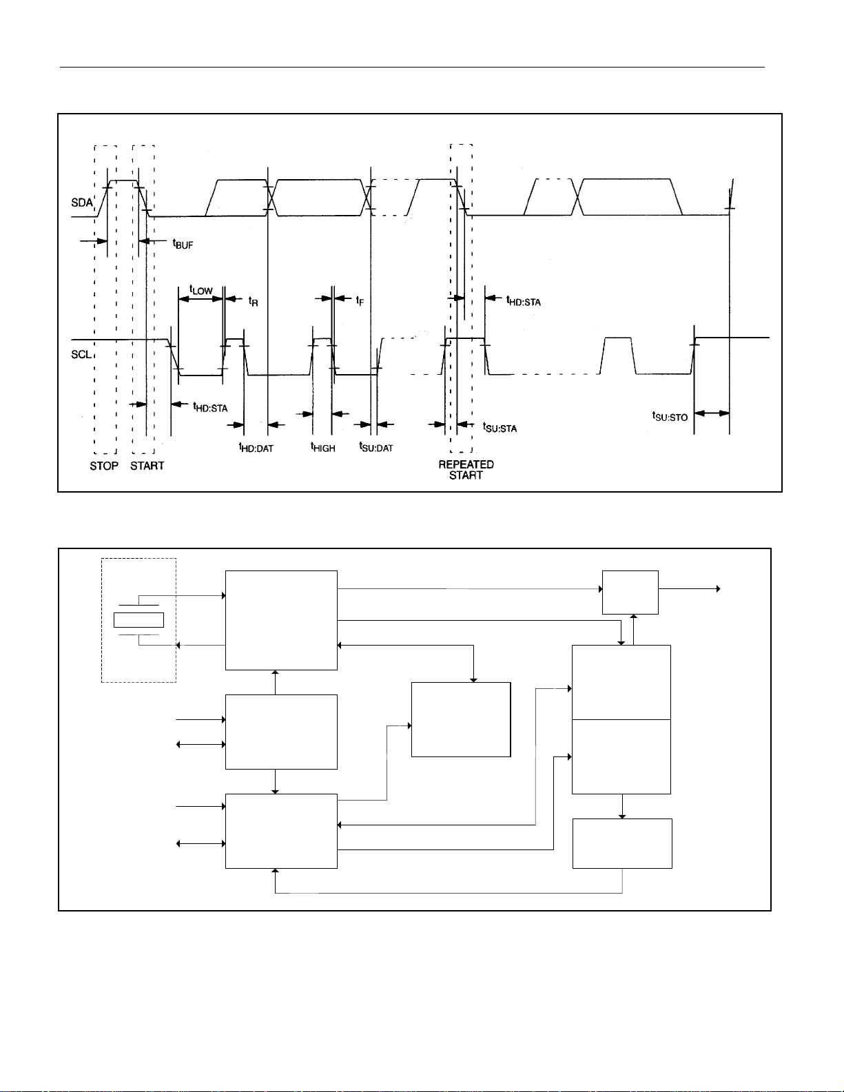
Figure 2. Timing Diagram
A
A
/
r
DS1339 I2C Serial Real-Time Clock
Figure 3. Block Diagram
X1
X2
V
CC
VBACKUP
SCL
SDA
OSCILLATOR AND
INTERFACE AND
"C" VERSION
ONLY
DIVIDER
POWER
CONTROL
SERIAL BUS
DDRESS
REGISTER
1Hz/4.096kHz/8.192kHz/32.768kHz
1Hz
CONTROL
LOGIC
Dallas Semiconducto
DS1339
MUX/
BUFFER
LARM,
TRICKLE
CHARGE, AND
CONTROL
REGISTERS
CLOCK AND
CALENDAR
REGISTERS
USER BUFFER
(7 BYTES)
SQW
INT
6 of 18
DS1339 I2C Serial Real-Time Clock
PIN DESCRIPTION
PIN
mSOP
SO
1 — X1
2 — X2
3 14 V
4 15 GND Ground. DC power is provided to the device on these pins.
5 16 SDA
6 1 SCL
7 2
8 3 VCC Power Supply. DC power is provided to the device on these pins.
— 4–13 N.C. No Connection. These pins are unused and must be connected to ground.
NAME FUNCTION
Connections for Standard 32.768kHz Quartz Crystal. The internal oscillator
circuitry is designed for operation with a crystal having a specified load
capacitance (C
) of 6pF. An external 32.768kHz oscillator can also drive the
L
DS1339. In this configuration, the X1 pin is connected to the external oscillator
signal and the X2 pin is floated.
For more information about crystal selection and crystal layout considerations,
refer to Application Note 58: Crystal Considerations with Dallas Real-Time
Clocks.
Secondary Power Supply. Supply voltage must be held between 1.3V and 3.7V
for proper operation. This pin can be connected to a primary cell, such as a
lithium button cell. Additionally, this pin can be connected to a rechargeable cell
BACKUP
should not be placed in series between the battery and the V
BACKUP
or a super cap when used in conjunction with the trickle-charge feature. Diodes
improper operation will result. UL recognized to ensure against reverse charging
current when used with a lithium battery If a back up supply is not required,
V
Serial Data Input/Output. SDA is the input/output pin for the I
must be grounded.
BACKUP
2
C serial interface.
The SDA pin is an open-drain output and requires an external pullup resistor.
Serial Clock Input. SCL is used to synchronize data movement on the serial
interface.
Square-Wave/Interrupt Output. Programmable square-wave or interrupt output
SQW/
INT
signal. The SQW/INT pin is an open-drain output and requires an external pullup
resistor.
TYPICAL OPERATING CIRCUIT
RPU RPU
VCC
CPU
VCC
6
5
CRYSTAL
12
X2X1
SCL
SDA
SQW/INT
DS1339
V
GND
4
BACKUP
VCC
VCC
8
7
i
3
input, or
7 of 18

DS1339 I2C Serial Real-Time Clock
DETAILED DESCRIPTION
The DS1339 serial real-time clock (RTC) is a low-power clock/date device with two programmable time-of-day
alarms and a programmable square-wave output. Address and data are transferred serially through an I
The clock/date provides seconds, minutes, hours, day, date, month, and year information. The date at the end of
the month is automatically adjusted for months with fewer than 31 days, including corrections for leap year. The
clock operates in either the 24-hour or 12-hour format with AM/PM indicator. The DS1339 has a built-in powersense circuit that detects power failures and automatically switches to the backup supply, maintaining time and
date operation.
2
C bus.
OPERATION
The DS1339 operates as a slave device on the serial bus. Access is obtained by implementing a START condition
and providing a device identification code followed by data. Subsequent registers can be accessed sequentially
until a STOP condition is executed. The device is fully accessible and data can be written and read when V
greater than V
is less than V
V
PF
greater than V
registers are maintained from the V
. However, when VCC falls below VPF, the internal clock registers are blocked from any access. If
PF
, the device power is switched from VCC to V
BACKUP
, the device power is switched from VCC to V
BACKUP
source until VCC is returned to nominal levels. The block diagram in
BACKUP
BACKUP
when VCC drops below VPF. If VPF is
BACKUP
when VCC drops below V
BACKUP
is
CC
. The
Figure 3 shows the main elements of the serial real-time clock.
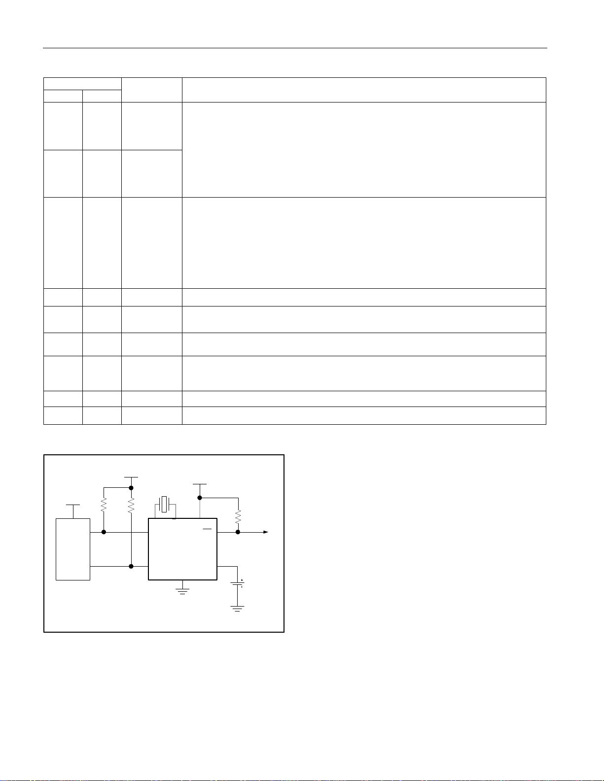
OSCILLATOR CIRCUIT
The DS1339 uses an external 32.768kHz crystal. The oscillator circuit does not require any external resistors or
capacitors to operate. Table 1 specifies several crystal parameters for the external crystal. Figure 4 shows a
functional schematic of the oscillator circuit. The startup time is usually less than 1 second when using a crystal
with the specified characteristics.
8 of 18

DS1339 I2C Serial Real-Time Clock
A
Table 1. Crystal Specifications*
PARAMETER SYMBOL MIN TYP MAX UNITS
Nominal Frequency fO 32.768 kHz
Series Resistance ESR 45
Load Capacitance CL 6 pF
*The crystal, traces, and crystal input pins should be isolated from RF generating signals. Refer to
Application Note 58: Crystal Considerations for Dallas Real-Time Clocks for additional specifications.
kW
Figure 4. Oscillator Circuit Showing Internal Bias Network
RTC
COUNTDOWN
CHAIN
C L 1 C L 2
RTC
REGISTERS
X1
X2
CRYSTAL
CLOCK ACCURACY
The accuracy of the clock is dependent upon the accuracy of the crystal and the accuracy of the match between
the capacitive load of the oscillator circuit and the capacitive load for which the crystal was trimmed. Additional
error is added by crystal frequency drift caused by temperature shifts. External circuit noise coupled into the
oscillator circuit may result in the clock running fast. Figure 5 shows a typical PC board layout for isolating the
crystal and oscillator from noise. Refer to Application Note 58: Crystal Considerations with Dallas Real-Time
Clocks for detailed information
DS1339C ONLY
The DS1339C integrates a standard 32,768Hz crystal in the package. Typical accuracy at nominal VCC and +25°C
is approximately 10ppm. Refer to Application Note 58 for information about crystal accuracy vs. temperature.
Figure 5. Typical PC Board Layout for Crystal
LOCAL GROUND PLANE (LAYER 2)
CRYSTAL
X1
X2
NOTE: AVOID ROUTING SIGNALS IN
THE CROSSHATCHED AREA (UPPER
LEFT-HAND QUADRANT) OF THE
PACKAGE UNLESS THERE IS
GROUND PLANE BETWEEN THE
SIGNAL LINE AND THE PACKAGE.
GND
9 of 18

DS1339 I2C Serial Real-Time Clock
ADDRESS MAP
Figure 6 shows the address map for the DS1339 registers. During a multibyte access, when the address pointer
reaches the end of the register space (10h), it wraps around to location 00h. On an I
pointer incrementing to location 00h, the current time is transferred to a second set of registers. The time
information is read from these secondary registers, while the clock may continue to run. This eliminates the need
to re-read the registers in case of an update of the main registers during a read.
Figure 6. Timekeeper Registers
ADDRESS BIT 7 BIT 6 BIT 5 BIT 4 BIT 3 BIT 2 BIT 1 BIT 0 FUNCTION RANGE
00H 0 10 Seconds Seconds Seconds 00–59
01H 0 10 Minutes Minutes Minutes 00–59
02H 0
03H 0 0 0 0 0 Day Day 1–7
04H 0 0 10 Date Date Date 01–31
05H Century 0 0
06H 10 Year Year Year 00–99
07H A1M1 10 Seconds Seconds
08H A1M2 10 Minutes Minutes
09H A1M3
0AH A1M4 DY/DT 10 Date Day, Date
0BH A2M2 10 Minutes Minutes
0CH A2M3
0DH A2M4
0EH
0FH OSF 0 0 0 0 0 A2F A1F Status
10H TCS3 TCS2 TCS1 TCS0 DS1 DS0
EOSC
12/24
12/24
12/24
DY/DT
0 0 RS2 RS1 INTCN A2IE A1IE Control
AM/PM
10 Hour
AM/PM
10 Hour
AM/PM
10 Hour
10 Hour Hour Hours
10
Month
10 Hour Hour
10 Hour Hour
10 Date Day, Date
Month
ROUT1 ROUT0
2
C START, STOP, or address
1–12
+AM/PM
00–23
Month/
Century
Alarm 1
Seconds
Alarm 1
Minutes
Alarm 1
Hours
Alarm 1
Day,
Alarm 1
Date
Alarm 2
Minutes
Alarm 2
Hours
Alarm 2
Day,
Alarm 2
Date
Trickle
Charger
01–12 +
Century
00–59
00–59
1–12 +
AM/PM
00–23
1-7, 1-31
00–59
1–12 +
AM/PM
00–23
1–7, 1–31
Note: Unless otherwise specified, the state of the registers are not defined when power is first applied or when VCC and V
V
BACKUP(MIN)
.
10 of 18
falls below the
BACKUP

DS1339 I2C Serial Real-Time Clock
TIME AND DATE OPERATION
The time and date information is obtained by reading the appropriate register bytes. Figure 6 shows the RTC
registers. The time and date are set or initialized by writing the appropriate register bytes. The contents of the time
and date registers are in the BCD format. The DS1339 can be run in either 12-hour or 24-hour mode. Bit 6 of the
hours register is defined as the 12- or 24-hour mode-select bit. When high, the 12-hour mode is selected. In the
12-hour mode, bit 5 is the
(20 to 23 hours). All hours values, including the alarms, must be re-entered whenever the 12/
changed. The century bit (bit 7 of the month register) is toggled when the years register overflows from 99 to 00.
The day-of-week register increments at midnight. Values that correspond to the day of week are user-defined, but
must be sequential (i.e., if 1 equals Sunday, then 2 equals Monday and so on). Illogical time and date entries result
in undefined operation.
When reading or writing the time and date registers, secondary (user) buffers are used to prevent errors when the
internal registers update. When reading the time and date registers, the user buffers are synchronized to the
internal registers on any start or stop, and when the address pointer rolls over to zero. The countdown chain is
reset whenever the seconds register is written. Write transfers occurs on the acknowledge pulse from the device.
To avoid rollover issues, once the countdown chain is reset, the remaining time and date registers must be written
within one second. If enabled, the 1Hz square-wave output transitions high 500ms after the seconds data transfer,
provided the oscillator is already running.
AM/PM bit with logic high being PM. In the 24-hour mode, bit 5 is the second 10-hour bit
24-hour mode bit is
ALARMS
The DS1339 contains two time of day/date alarms. Alarm 1 can be set by writing to registers 07h to 0Ah. Alarm 2
can be set by writing to registers 0Bh to 0Dh. The alarms can be programmed (by the Alarm Enable and INTCN
bits of the Control Register) to activate the SQW/
of day/date alarm registers are mask bits (Table 2). When all the mask bits for each alarm are logic 0, an alarm
only occurs when the values in the timekeeping registers 00h to 06h match the values stored in the time of
day/date alarm registers. The alarms can also be programmed to repeat every second, minute, hour, day, or date.
Table 2 shows the possible settings. Configurations not listed in the table result in illogical operation.
The DY/
register reflects the day of the week or the date of the month. If DY/
of a match with date of the month. If DY/
week.
The device checks for an alarm match once per second. When the RTC register values match alarm register
settings, the corresponding Alarm Flag ‘A1F’ or ‘A2F’ bit is set to logic 1. If the corresponding Alarm Interrupt
Enable ‘A1IE’ or ‘A2IE’ is also set to logic 1 and the INTCN bit is set to logic 1, the alarm condition activates the
SQW/
The alarm output remains active until the alarm flag is cleared by the user.
DT bits (bit 6 of the alarm day/date registers) control whether the alarm value stored in bits 0 to 5 of that
DT is written to a logic 1, the alarm is the result of a match with day of the
INT) signal. If the BBSQI bit is set to 1, the INT output activates while the part is being powered by V
INT output on an alarm match condition. Bit 7 of each of the time
DT is written to a logic 0, the alarm is the result
BACKUP
.
11 of 18

DS1339 I2C Serial Real-Time Clock
Table 2. Alarm Mask Bits
ALARM 1 REGISTER MASK BITS
DY/DT
(Bit 7)
ALARM RATE
A1M4 A1M3 A1M2 A1M1
X 1 1 1 1 Alarm once per second
X 1 1 1 0 Alarm when seconds match
X 1 1 0 0 Alarm when minutes and seconds match
X 1 0 0 0 Alarm when hours, minutes, and seconds match
0 0 0 0 0
Alarm when date, hours, minutes, and seconds
match
1 0 0 0 0 Alarm when day, hours, minutes, and seconds match
ALARM 2 REGISTER MASK BITS
DY/DT
(Bit 7)
ALARM RATE
A2M4 A2M3 A2M2
X 1 1 1 Alarm once per minute (00 sec. of every min.)
X 1 1 0 Alarm when minutes match
X 1 0 0 Alarm when hours and minutes match
0 0 0 0 Alarm when date, hours, and minutes match
1 0 0 0 Alarm when day, hours, and minutes match
SPECIAL-PURPOSE REGISTERS
The DS1339 has two additional registers (control and status) that control the RTC, alarms, and square-wave
output.
CONTROL REGISTER (0Eh)
BIT 7 BIT 6 BIT 5 BIT 4 BIT 3 BIT 2 BIT 1 BIT 0
EOSC
0 BBSQI RS2 RS1 INTCN A2IE A1IE
Bit 7: Enable Oscillator
(EOSC). This bit when set to logic 0 starts the oscillator. When this bit is set to a logic 1,
the oscillator is stopped. This bit is enabled (logic 0) when power is first applied.
Bit 5: Battery-Backed Square-Wave and Interrupt Enable (BBSQI). This bit when set to a logic 1 enables the
square wave or interrupt output when V
BBSQI is a logic 0, the SQW/
INT pin goes high impedance when V
is absent and the DS1339 is being powered by the V
CC
falls below the power-fail trip point. This bit is
CC
BACKUP
pin. When
disabled (logic 0) when power is first applied.
Bits 4 and 3: Rate Select (RS2 and RS1). These bits control the frequency of the square-wave output when the
square wave has been enabled. The table below shows the square-wave frequencies that can be selected with the
RS bits. These bits are both set to logic 1 (32kHz) when power is first applied.
Square-Wave Output Frequency
SQUARE-WAVE
RS2 RS1
0 0 1Hz
0 1 4.096kHz
1 0 8.192kHz
1 1 32.768kHz
OUTPUT
FREQUENCY
12 of 18

DS1339 I2C Serial Real-Time Clock
Bit 2: Interrupt Control (INTCN). This bit controls the relationship between the two alarms and the interrupt output
pins. When the INTCN bit is set to logic 1, a match between the timekeeping registers and the alarm 1 or alarm 2
registers activate the SQW/
square wave is output on the SQW/
INT pin (provided that the alarm is enabled). When the INTCN bit is set to logic 0, a
INT pin. This bit is set to logic 0 when power is first applied.
Bit 1: Alarm 2 Interrupt Enable (A2IE). When set to a logic 1, this bit permits the Alarm 2 Flag (A2F) bit in the
status register to assert SQW/
INT (when INTCN = 1). When the A2IE bit is set to logic 0 or INTCN is set to logic 0,
the A2F bit does not initiate an interrupt signal. The A2IE bit is disabled (logic 0) when power is first applied.
Bit 0: Alarm 1 Interrupt Enable (A1IE). When set to logic 1, this bit permits the Alarm 1 Flag (A1F) bit in the
status register to assert SQW/
INT (when INTCN = 1). When the A1IE bit is set to logic 0 or INTCN is set to logic 0,
the A1F bit does not initiate an interrupt signal. The A1IE bit is disabled (logic 0) when power is first applied.
STATUS REGISTER (0Fh)
BIT 7 BIT 6 BIT 5 BIT 4 BIT 3 BIT 2 BIT 1 BIT 0
OSF 0 0 0 0 0 A2F A1F
Bit 7: Oscillator Stop Flag (OSF). A logic 1 in this bit indicates that the oscillator either is stopped or was stopped
for some period of time and may be used to judge the validity of the clock and date data. This bit is edge triggered
and is set to logic 1 when the oscillator stops. The following are examples of conditions that can cause the OSF bit
to be set:
1) The first time power is applied.
2) The voltage on both V
3) The
EOSC bit is turned off.
4) External influences on the crystal (e.g., noise, leakage, etc.).
This bit remains at logic 1 until written to logic 0. This bit can only be written to a logic 0.
Bit 1: Alarm 2 Flag (A2F). A logic 1 in the Alarm 2 Flag bit indicates that the time matched the alarm 2 registers. If
the A2IE bit is a logic 1 and the INTCN bit is set to a logic 1, the SQW/
when written to logic 0. This bit can only be written to logic 0. Attempting to write to logic 1 leaves the value
unchanged.
Bit 0: Alarm 1 Flag (A1F). A logic 1 in the Alarm 1 Flag bit indicates that the time matched the alarm 1 registers. If
the A1IE bit is a logic 1 and the INTCN bit is set to a logic 1, the SQW/
when written to logic 0. This bit can only be written to logic 0. Attempting to write to logic 1 leaves the value
unchanged.
and V
CC
are insufficient to support oscillation.
BACKUP
INT pin is also asserted. A2F is cleared
INT pin is also asserted. A1F is cleared
13 of 18

DS1339 I2C Serial Real-Time Clock
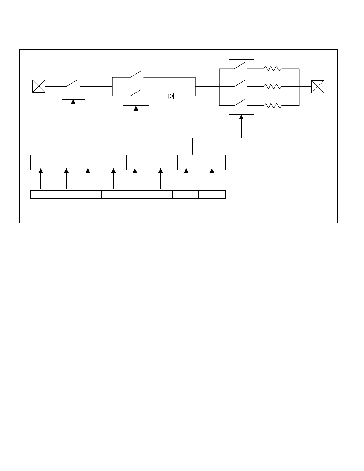
TRICKLE CHARGER REGISTER (10h)
The simplified schematic in Figure 7 shows the basic components of the trickle charger. The trickle-charge select
(TCS) bits (bits 4 to 7) control the selection of the trickle charger. To prevent accidental enabling, only a pattern on
1010 enables the trickle charger. All other patterns disable the trickle charger. The trickle charger is disabled when
power is first applied. The diode-select (DS) bits (bits 2 and 3) select whether or not a diode is connected between
V
and V
CC
. The ROUT bits (bits 0 and 1) select the value of the resistor connected between VCC and V
BACKUP
BACKUP
Table 3 shows the bit values.
Table 3. Trickle Charger Register (10h)
.
BIT 7 BIT 6 BIT 5 BIT 4 BIT 3 BIT 2 BIT 1 BIT 0
TCS3 TCS2 TCS1 TCS0 DS1 DS0 ROUT1 ROUT0
FUNCTION
X X X X 0 0 X X Disabled
X X X X 1 1 X X Disabled
X X X X X X 0 0 Disabled
1 0 1 0 0 1 0 1
1 0 1 0 1 0 0 1
1 0 1 0 0 1 1 0
1 0 1 0 1 0 1 0
1 0 1 0 0 1 1 1
1 0 1 0 1 0 1 1
No diode, 250W resistor
One diode, 250W resistor
No diode, 2kW resistor
One diode, 2kW resistor
No diode, 4kW resistor
One diode, 4kW resistor
0 0 0 0 0 0 0 0 Initial power-up values
The user determines diode and resistor selection according to the maximum current desired for battery or super
cap charging. The maximum charging current can be calculated as illustrated in the following example. Assume
that a 3.3V system power supply is applied to V
trickle charger has been enabled with a diode and resistor R2 between V
and a super cap is connected to V
CC
and V
CC
. Also assume that the
BACKUP
. The maximum current I
BACKUP
MAX
would therefore be calculated as follows:
I
= (3.3V - diode drop) / R2 » (3.3V - 0.7V) / 2kW » 1.3mA
MAX
As the super cap or battery charges, the voltage drop between V
and V
CC
decreases and therefore the
BACKUP
charge current decreases.
14 of 18
DS1339 I2C Serial Real-Time Clock
Figure 7. Programmable Trickle Charger
VCC
NOTE: ONLY 1010 ENABLES CHARGER
TCS3 TCS2 TCS1 TCS0 DS1 DS0 ROUT1 ROUT0
BIT 7 BIT 6 BIT 5 BIT 4 BIT 3 BIT 2 BIT 1 BIT 0
1 OF 16 SELECT
TRICKLE CHARGE REGISTER
1 OF 2
SELECT
1 OF 3
SELECT
TCS
= TRICKLE CHARGER SELECT
0-3
= DIODE SELECT
DS
0-1
ROUT
0-1
R1
250W
R2
2kW
R3
4kW
= RESISTOR SELECT
V
BACKUP
I2C SERIAL DATA BUS
The DS1339 supports the I2C bus protocol. A device that sends data onto the bus is defined as a transmitter and a
device receiving data as a receiver. The device that controls the message is called a master. The devices that are
controlled by the master are referred to as slaves. The bus must be controlled by a master device that generates
the serial clock (SCL), controls the bus access, and generates the START and STOP conditions. The DS1339
operates as a slave on the I
mode (400kHz cycle rate) are defined. The DS1339 works in both modes. Connections to the bus are made via the
open-drain I/O lines SDA and SCL.
The following bus protocol has been defined (Figure 8):
§ Data transfer may be initiated only when the bus is not busy.
§ During data transfer, the data line must remain stable whenever the clock line is HIGH. Changes in the data
line while the clock line is HIGH are interpreted as control signals.
Accordingly, the following bus conditions have been defined:
Bus not busy: Both data and clock lines remain HIGH.
Start data transfer: A change in the state of the data line, from HIGH to LOW, while the clock is HIGH, defines a
START condition.
Stop data transfer: A change in the state of the data line, from LOW to HIGH, while the clock line is HIGH,
defines the STOP condition.
Data valid: The state of the data line represents valid data when, after a START condition, the data line is stable
for the duration of the HIGH period of the clock signal. The data on the line must be changed during the LOW
period of the clock signal. There is one clock pulse per bit of data.
2
C bus. Within the bus specifications, a standard mode (100kHz cycle rate) and a fast
15 of 18

DS1339 I2C Serial Real-Time Clock
Each data transfer is initiated with a START condition and terminated with a STOP condition. The number of data
bytes transferred between START and STOP conditions is not limited, and is determined by the master device.
The information is transferred byte-wise and each receiver acknowledges with a ninth bit.
Acknowledge: Each receiving device, when addressed, is obliged to generate an acknowledge after the reception
of each byte. The master device must generate an extra clock pulse that is associated with this acknowledge bit.
A device that acknowledges must pull down the SDA line during the acknowledge clock pulse in such a way that
the SDA line is stable LOW during the HIGH period of the acknowledge related clock pulse. Of course, setup and
hold times must be taken into account. A master must signal an end of data to the slave by not generating an
acknowledge bit on the last byte that has been clocked out of the slave. In this case, the slave must leave the data
line HIGH to enable the master to generate the STOP condition.
Figure 8. Data Transfer on I2C Serial Bus
Depending upon the state of the R/W bit, two types of data transfer are possible:
1) Data transfer from a master transmitter to a slave receiver. The first byte transmitted by the master is the
slave address. Next follows a number of data bytes. The slave returns an acknowledge bit after each received
byte. Data is transferred with the most significant bit (MSB) first.
2) Data transfer from a slave transmitter to a master receiver. The first byte (the slave address) is transmitted
by the master. The slave then returns an acknowledge bit. This is followed by the slave transmitting a number
of data bytes. The master returns an acknowledge bit after all received bytes other than the last byte. At the
end of the last received byte, a “not acknowledge” is returned. The master device generates all of the serial
clock pulses and the START and STOP conditions. A transfer is ended with a STOP condition or with a
repeated START condition. Since a repeated START condition is also the beginning of the next serial transfer,
the bus is not released. Data is transferred with the most significant bit (MSB) first.
The DS1339 can operate in the following two modes:
1) Slave Receiver Mode (Write Mode): Serial data and clock are received through SDA and SCL. After each
byte is received an acknowledge bit is transmitted. START and STOP conditions are recognized as the
beginning and end of a serial transfer. Address recognition is performed by hardware after reception of the
slave address and direction bit (Figure 9). The slave address byte is the first byte received after the START
condition is generated by the master. The slave address byte contains the 7-bit DS1339 address, which is
1101000, followed by the direction bit (R/
address byte the slave outputs an acknowledge on the SDA line. After the DS1339 acknowledges the slave
address + write bit, the master transmits a register address to the DS1339. This sets the register pointer on the
DS1339, with the DS1339 acknowledging the transfer. The master may then transmit zero or more bytes of
W), which is 0 for a write. After receiving and decoding the slave
16 of 18

DS1339 I2C Serial Real-Time Clock
W
data, with the DS1339 acknowledging each byte received. The address pointer increments after each data
byte is transferred. The master generates a STOP condition to terminate the data write.
2) Slave Transmitter Mode (Read Mode): The first byte is received and handled as in the slave receiver mode.
However, in this mode, the direction bit indicates that the transfer direction is reversed. Serial data is
transmitted on SDA by the DS1339 while the serial clock is input on SCL. START and STOP conditions are
recognized as the beginning and end of a serial transfer (Figure 10). The slave address byte is the first byte
received after the START condition is generated by the master. The slave address byte contains the 7-bit
DS1339 address, which is 1101000, followed by the direction bit (R/
and decoding the slave address byte the slave outputs an acknowledge on the SDA line. The DS1339 then
begins to transmit data starting with the register address pointed to by the register pointer. If the register
pointer is not written to before the initiation of a read mode the first address that is read is the last one stored in
the register pointer. The address pointer is incremented after each byte is transferred. The DS1339 must
receive a “not acknowledge” to end a read.
W), which is 1 for a read. After receiving
Figure 9. Data Write—Slave Receiver Mode
slave address
S
1101000
W
R/
register address (n)
0 A
XXXXXXXX
A
XXXXXXXX
Data (n) Data (n+1) Data (n+x)
S - START
A - ACKNOWLEDGE
P - STOP
R/W - READ/WRITE OR DIRECTION BIT
(X+1 BYTES + ACKNOWLEDGE)
Figure 10. Data Read—Slave Transmitter Mode
slave address
S
1101000
W
R/
1 A
Data (n)
XXXXXXXX
Data (n+1) Data (n+x) Data (n+2)
A
XXXXXXXX
S - START
A - ACKNOWLEDGE
P - STOP
/A - NOT ACKNOWLEDGE
R/
- READ/WRITE OR DIRECTION BIT
A
XXXXXXXX
DATA TRANSFERRED
A
XXXXXXXX
DATA TRANSFERRED
(X+1 BYTES + ACKNOWLEDGE)
A
XXXXXXXX
A
XXXXXXXX /A
P
17 of 18
DS1339 I2C Serial Real-Time Clock
T
C
HANDLING, PC BOARD LAYOUT, AND ASSEMBLY
The DS1339C package contains a quartz tuning-fork crystal. Pick-and-place equipment may be used, but
precautions should be taken to ensure that excessive shocks are avoided. Ultrasonic cleaning should be avoided
to prevent damage to the crystal.
Avoid running signal traces under the package, unless a ground plane is placed between the package and the
signal line. All N.C. (no connect) pins must be connected to ground.
The SO package may be reflowed as long as the peak temperature does not exceed 240°C. Peak reflow
temperature (≥ 230°C) duration should not exceed 10 seconds, and the total time above 200°C should not exceed
40 seconds (30 seconds nominal). Exposure to reflow is limited to 2 times maximum.
Moisture-sensitive packages are shipped from the factory dry-packed. Handling instructions listed on the package
label must be followed to prevent damage during reflow. Refer to the IPC/JEDEC J-STD-020B standard for
moisture-sensitive device (MSD) classifications.
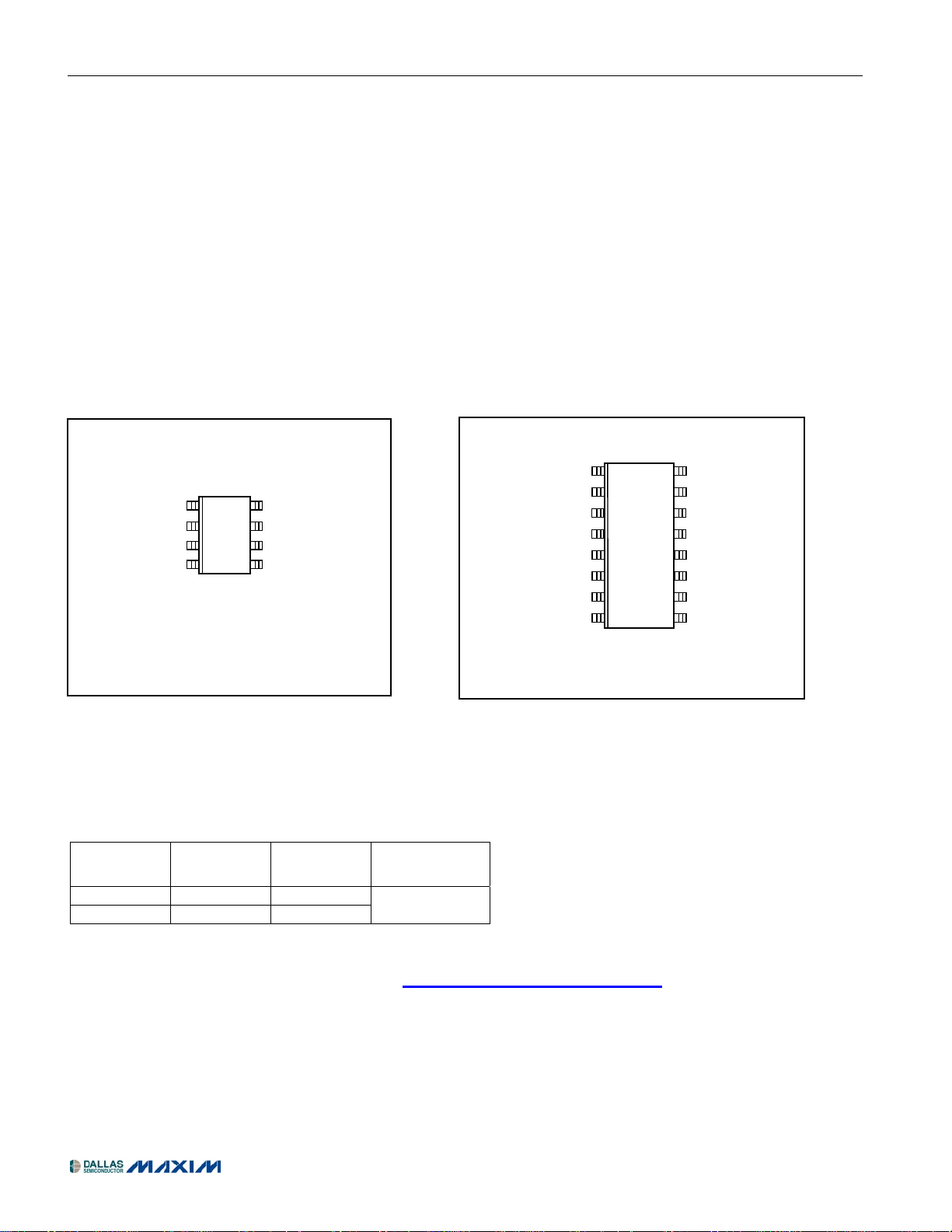
PIN CONFIGURATIONS
TOP VIEW
V
BACKUP
X1
X2
GND
DS1339
mSOP
V
CC
SQW/INT
SCL
SDA
TOP VIEW
SCL SDA
SQW/IN
V
N.C.
N.C.
N.C.
N.C.
N.C.
CC
DS1339
SO (300 mils)
GND
V
BACKUP
N.C.
N.C.
N.C.
N.C.
N.C.
CHIP INFORMATION
TRANSISTOR COUNT: 11,325
PROCESS: CMOS
THERMAL INFORMATION
PART
THETA-J
(°C/W)
µSOP 229 39
SO 73 23
A
THETA-JC
(°C/W)
CONDITIONS
Typical
PACKAGE INFORMATION
For the latest package outline information, go to www.maxim-ic.com/DallasPackInfo.
18 of 18
Maxim/Dallas Semiconductor cannot assume responsibility for use of any circuitry other than circuitry entirely embodied in a Maxim/Dallas Semiconductor product.
No circuit patent licenses are implied. Maxim/Dallas Semiconductor reserves the right to change the circuitry and specifications without notice at any time.
Maxim Integrated Products, 120 San Gabriel Drive, Sunnyvale, CA 94086 408-737-7600
are registered trademarks of Maxim Integrated Products, Inc., and Dallas Semiconductor Corporation.
© 2005 Maxim Integrated Products · Printed USA
 Loading...