

Page 1
I
I
19-5056; Rev 12/09
www.maxim-ic.com
FEATURES
Real-Time Clock (RTC) Counts Seconds,
Minutes, Hours, Date of the Month, Month,
Day of the Week, and Year with Leap-Year
Compensation Valid Up to 2100
96-Byte, Battery-Backed NV RAM for Data
Storage
Two Time-of-Day Alarms, Programmable on
Combination of Seconds, Minutes, Hours,
and Day of the Week
1Hz and 32.768kHz Clock Outputs
Supports Motorola SPI™ (Serial Peripheral
Interface) Modes 1 and 3 or Standard 3-Wire
Interface
Burst Mode for Reading/Writing Successive
Addresses in Clock/RAM
Dual-Power Supply Pins for Primary and
Backup Power Supplies
Optional Trickle Charge Output to Backup
Supply
2.0V to 5.5V Operation
Optional Industrial Temperature Range:
-40°C to +85°C
Available in Space-Efficient, 20-Pin TSSOP
Package
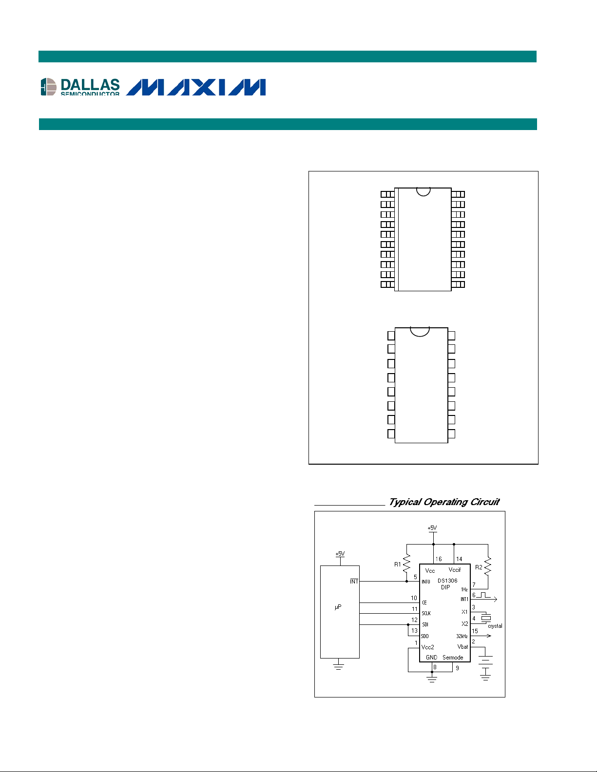
Serial Alarm Real-Time Clock
PIN CONFIGURATIONS
V
CC2
V
BAT
X1
N.C.
X2
N.C.
NT0
INT1
1Hz
GND
V
V
NT0
INT1
1Hz
GND
CC2
BAT
X1
X2
1
2
3
4
5
6
7
8
9
10
20
19
18
17
16
15
14
13
12
11
TSSOP (4.4mm)
1
2
3
4
5
6
7
8
16
15
14
13
12
11
10
DIP (300 mils)
9
DS1306
V
CC1
N.C.
32kHz
V
CCIF
SDO
SDI
SCLK
N.C.
CE
SERMODE
V
CC1
32kHz
V
CCIF
SDO
SDI
SCLK
CE
SERMODE
Underwriters Laboratory (UL) Recognized
SPI is a trademark of Motorola, Inc.
1 of 22
Page 2

ORDERING INFORMATION
PART TEMP RANGE PIN-PACKAGE TOP MARK*
DS1306 0°C to +70°C 16 DIP (300 mils) DS1306
DS1306+ 0°C to +70°C 16 DIP (300 mils) DS1306 +
DS1306N -40°C to +85°C 16 DIP (300 mils) DS1306N
DS1306N+ 0°C to +70°C 16 DIP (300 mils) DS1306N +
DS1306E 0°C to +70°C 20 TSSOP (173 mils) DS1306
DS1306E+ 0°C to +70°C 20 TSSOP (173 mils) DS1306 +
DS1306EN -40°C to +85°C 20 TSSOP (173 mils) DS1306N
DS1306EN+ -40°C to +85°C 20 TSSOP (173 mils) DS1306N +
DS1306EN/T&R -40°C to +85°C 20 TSSOP (173 mils) DS1306N
DS1306EN+T&R -40°C to +85°C 20 TSSOP (173 mils) DS1306N +
DS1306E/T&R 0°C to +70°C 20 TSSOP (173 mils) DS1306
DS1306E+T&R 0°C to +70°C 20 TSSOP (173 mils) DS1306 +
+Denotes a lead(Pb)-free/RoHS-compliant package
T&R = Tape and reel.
*An “N” on the top mark indicates an industrial device.
PIN DESCRIPTION
PIN
TSSOP DIP
1 1 V
2 2 V
3 3 X1
5 4 X2
7 5
8 6 INT1
NAME FUNCTION
Backup Power Supply. This is the secondary power supply pin. In systems
using the trickle charger, the rechargeable energy source is connected to this
CC2
pin.
Battery Input for Any Standard +3V Lithium Cell or Other Energy
BAT
Source. If not used, V
placed in series between V
result. UL recognized to ensure against reverse charging current when used
must be connected to ground. Diodes must not be
BAT
and the battery, or improper operation will
BAT
in conjunction with a lithium battery. See “Conditions of Acceptability” at
www.maxim-ic.com/TechSupport/QA/ntrl.htm
.
Connections for Standard 32.768kHz Quartz Crystal. The internal
oscillator is designed for operation with a crystal having a specified load
capacitance of 6pF. For more information on crystal selection and crystal
layout considerations, refer to Application Note 58, “Crystal Considerations
with Dallas Real-Time Clocks.” The DS1306 can also be driven by an
external 32.768kHz oscillator. In this configuration, the X1 pin is connected
to the external oscillator signal and the X2 pin is floated.
Active-Low Interrupt 0 Output. The INT0 pin is an active-low output of
the DS1306 that can be used as an interrupt input to a processor. The INT0
pin can be programmed to be asserted by Alarm 0. The INT0 pin remains
INT0
low as long as the status bit causing the interrupt is present and the
corresponding interrupt enable bit is set. The INT0 pin operates when the
DS1306 is powered by V
CC1
CC2
, or V
. The INT0 pin is an open-drain
BAT
, V
output and requires an external pullup resistor.
Interrupt 1 Output. The INT1 pin is an active-high output of the DS1306
that can be used as an interrupt input to a processor. The INT1 pin can be
programmed to be asserted by Alarm 1. When an alarm condition is present,
the INT1 pin generates a 62.5ms active-high pulse. The INT1 pin operates
only when the DS1306 is powered by V
pin is internally pulled up to V
CC2
or V
or V
CC2
. When inactive, the INT1 pin is
BAT
. When active, the INT1
BAT
internally pulled low.
2 of 22
DS1306
 Loading...