

Page 1
CE
WE
OE
DS1225AB/AD
64k Nonvolatile SRAM
www.maxim-ic.com
15
13
27
A7
A5
A3
A2
A1
A0
DQ0
DQ1
GND
DQ2
VCC
NC
A8
A9
A11
OE
A10
CE
DQ7
DQ6
DQ5
DQ3
DQ4
1
2
3 4 5
6 7 8
9
10
11
12
14
28
26
25
24
23
22
21
20
19
18
17
16
A12
A6
A4
NC
19-5625; Rev 11/10
FEATURES
10 years minimum data r etent ion in the
absence of external power
Data is automatically pro tected during power
loss
Directly replaces 8k x 8 volatile static RAM
or EE P R O M
Unlimited write c ycles
Low-power CMOS
JEDEC standard 28-pin DIP pack age
Read and write access times of 70 ns
Lithium energy sour ce is electrically
disconnected to retain freshness until power
is applied for the first time
Full ±10% VCC operating range (DS1225AD)
Optio na l ±5% V
(DS1225AB)
Optional industrial temperature range of
-40°C to +85°C, designated IND
operat ing range
CC
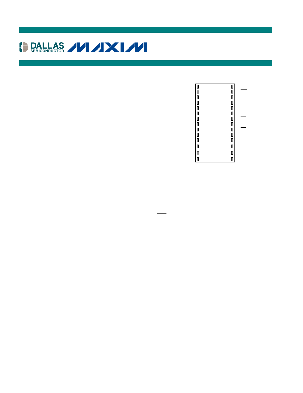
PIN ASSIGNMENT
28-Pin ENCAPSULATED PACKAGE
720-mil EXTENDED
PIN DESCRIPTION
A0-A12 - Address Inputs
DQ0-DQ7 - Data In/Data Out
- Chip Enable
- Write Enable
- Output Enable
V
- Power (+5V)
CC
GND - Ground
NC - No Co nne ct
DESCRIPTION
The DS1225AB and DS1225AD are 65,536-bit, fully static, nonvolatile SRAMs organized as 8192 words
by 8 bits. Each NV SRAM has a self-contained lithium energy source and control circuitry which
constantly monitors VCC for an out-of-tolerance condition. When such a condition occurs, the lithium
energy source is automatically switched on and write protection is unconditio nally enabled to prevent
data corruption. The NV SRAMs can be used in place of existing 8k x 8 SRAMs directly conforming to
the popular bytewide 28-p in DIP standard. The devices also match the pinout of the 2764 EPROM and
the 2864 EEPROM, a llow ing dir ect s ubst itut ion wh ile en hanc ing pe rfor mance. Ther e is no lim it on t he
number of write cycles that can be executed and no additional support circuitry is required for
microprocesso r inter facing.
1 of 10
Page 2

READ MODE
WE
CE
OE
OE
WE
CE
WE
WE
WE
OE
WE
DS1225AB/AD
The DS1225AB and DS1225AD execute a read c ycle whenever
(Write Enable) is inactive (high) and
(Chip Enable) and OE(Output Enable) are active (low). The unique address specified by the 13
address inputs (A0 -A12) defines which of the 8192 bytes of data is to be accessed. Valid data will be
available to the eight data output drivers within t
stable, providing that CE and
access t imes a re als o sat isfied . If CE and
(Access T ime) after the last address input signal is
ACC
access t imes are not
satisfied, then data access must be measured fro m the later-oc cu rr ing s ig na l a nd t he li miting pa r a meter is
either tCO for CE or tOE for OE rather than address access.
WRITE MODE
The DS1225AB and DS1225AD execute a write cycle whenever the
(low) after addr ess inputs are st able. The later-occurring falling edge of CE or
start of the write cycle. The wr ite c ycle is ter minated by the ear lier r ising edge of CE or
inputs must be kept va lid t hroug hout the wr ite cy cle.
must ret urn to t he high s tat e for a min imu m
recovery t ime (tWR ) before ano ther c ycle can be initiated. The OE control signal should be kept inactive
(hig h) d ur ing wr ite cyc les t o avoid bus co ntent io n. Ho weve r, if t he ou tp ut d river s ar e e nable d (CE and
active) then
will disable the output s i n t
from its falling edge.
ODW
and
signals are active
w ill dete rmine t he
. All address
DATA RETENTION MODE
The DS1225AB provides full functional capability for VCC greater than 4.75 volts and write protects by
4.5 volts. The DS1225AD provides full-fu nctiona l capabilit y for VCC greater than 4.5 volts and write
protects by 4.25 volts. Data is maintained in the a bsence of VCC without any add itional support circuitry.
The nonvolatile stat ic RAMs constantly monitor VCC. Should the supply vo ltage decay, the NV SRAMs
automatically write protect themselves, all inputs become “don’t care,” and all outputs become highimpedance. As VCC falls below approximately 3.0 vo lts, the power switching circuit connect s the lithiu m
energy source to RAM to r etain data. During power-up , when VCC rises above approximately 3.0 volts,
the power sw itching c ircuit connect s external VCC to RAM and disconnects the lithium energy source.
Normal RAM operat ion can resu me after VCC exceeds 4.75 volts for the DS1225AB and 4.5 volts for the
DS1225AD.
FRESHNESS SEAL
Each DS1225 is shipped from Maxim with the lithium energy source disconnected, guaranteeing full
energy capacity. Whe n VCC is first applied at a level of great er than VTP , the lithium energ y source is
enabled for batt er y backup operation.
2 of 9
Page 3
DS1225AB/AD
PARAMETER
SYMBOL
MIN
TYP
MAX
UNITS
NOTES
DS1225AB Power Supply Voltage
VCC
4.75
5.0
5.25 V
DS1225AD Power Supply Voltage
VCC
4.50
5.0
5.5 V
Log ic 1
VIH
2.2 VCC V
Logic 0
VIL
0.0 +0.8 V
PARAMETER
SYMBOL
MIN
TYP
MAX
UNITS
NOTES
Input Leakage Current
A
I/O Leakage Current
CE
> VIH< VCC
Output Current @ 2.4V
IOH
-1.0
mA
Output Current @ 0.4V
IOL
2.0
mA
Standby Current CE =VCC -0.5V
Operating Current
(Commercial)
Operating Current
(Industrial)
Write Protection Voltage
(DS1225AB)
Write Protection Voltage
(DS1225AD)
PARAMETER
SYMBOL
MIN
TYP
MAX
UNITS
NOTES
Input Capacitance
CIN
5 10
pF
Input/Out put C apacitance
C
I/O
5 10
pF
ABSOLUTE MAXIMUM RATINGS
Voltage on Any Pin Relative to Ground -0.3V to +6.0V
Operating Temperat ur e
Commercial: 0°C to +70°C
Industrial: -40°C to +85°C
Storage Temperatu r e -40°C to +85°C
Lead Temperature (soldering, 10s) +260°C
Note: EDIP is wave or hand soldered only.
This is a stress rating only and functional operation of the device at these or any other conditions above those indicated in the operation
sections of this specification is not implied. Exposure to absolute maximum rating conditions for extended periods of time may affect
reliability.
RECOMMENDED DC OPERATING CONDITIONS (TA: See Note 10)
(TA: See Note 10)
(V
=5V ± 5% for DS1225AB)
CC
DC ELECTRICAL CHARACTERISTICS (V
=5V ± 10% for DS1225AD)
CC
Standby Current CE =2.2V
IIL -1.0 +1.0
IIO -1.0 +1.0
I
5.0 10.0 mA
CCS1
I
3.0 5.0 mA
CCS2
I
75 mA
CC01
I
85 mA
CC01
µ
µA
VTP 4.50 4.62 4.75 V
VTP 4.25 4.37 4.5 V
CAPACITANCE (TA = +25°C)
3 of 9
Page 4

AC ELECTRICAL CHARACTERISTICS (V
DS1225AB-70
DS1225AD-70
MIN
MAX
Read Cycle Time
tRC
70 ns
Acce ss Time
t
ACC
70
ns
OE
to Output Va lid
35
CE
70
CE
to Output Active
5
Outpu t H igh Z from De selection
tOD 25
ns
5
Output Hold from Address
5
Writ e Cycle Time
tWC
70 ns
Write Pulse Width
tWP
55 ns
3
Address Setup Time
tAW 0
ns
t
WR2
0
ns
12
Outpu t H igh Z from
WE
25
5
Data Setup Time
tDS
30 ns
4
t
t
DH2
0 10
ns
ns
12
13
DS1225AB/AD
(TA: See Note 10)
(V
=5V ± 5% for DS1225AB)
CC
=5V ± 10% for DS1225AD)
CC
PARAMETER SYMBOL
to O utput Va lid
OE or
Change
Write Recovery Time
Output Active from
WE
Data Hold Time
tOE
tCO
t
COE
tOH
WR1
t
t
ODW
t
OEW
DH1
10
UNITS NOTES
ns
ns
ns 5
ns
ns
13
ns 5
ns 5
4 of 9
Page 5
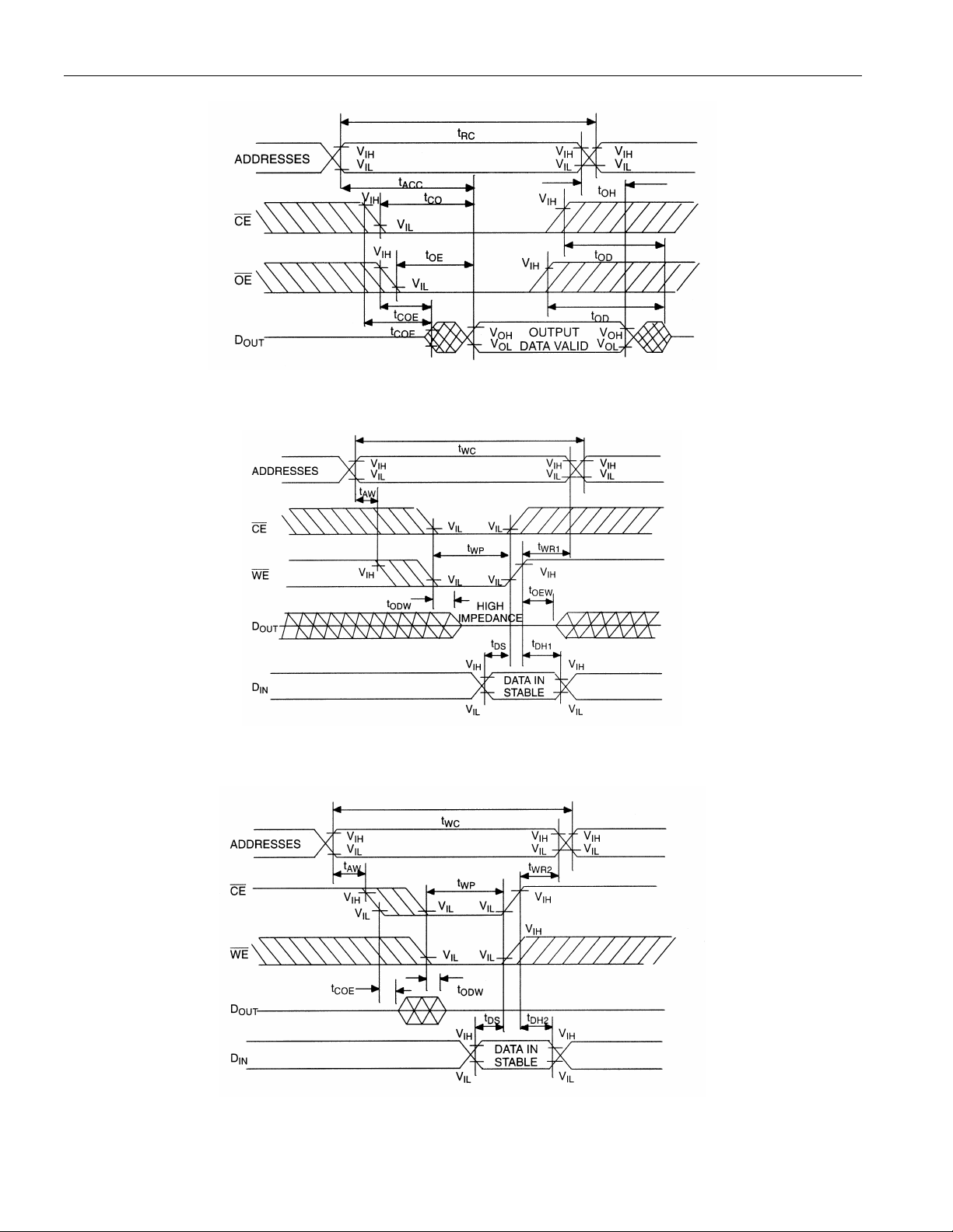
READ CYCLE
DS1225AB/AD
SEE NOTE 1
WRITE CYCLE 1
SEE NOTES 2, 3, 4, 6, 7, 8 AND 12
WRITE CYCLE 2
SEE NOTES 2, 3, 4, 6, 7, 8 AND 13
5 of 9
Page 6

POWER-DOWN/POWER-UP CONDITION
WE
Expected Dat a Retent ion T ime
tDR
10
years
9
DS1225AB/AD
SEE NOTE 11
POWER-DOWN/POWER-UP TIMING (T
PARAMETER SYMBOL MIN TYP MAX UNITS NOTES
VCC Fail Detect to CE and WE Inactive
VCC s lew from VTP to 0V t
VCC slew from 0V to VTP t
VCC Va lid to CE and
Inactive
VCC Valid to End of Write Protection t
t
PD
F
R
t
PU
REC
1.5
300
300
2 ms
125 ms
: See Note 10)
A
µs
11
µs
µs
(T
= +25°C)
A
PARAMETER SYMBOL MIN TYP MAX UNITS NOTES
WARNING:
Under no circumstance are negative undershoots, of any amplitude, allowed when device is in battery
backup mode.
6 of 9
Page 7

NOTES:
WE
OE
OE
WE
WE
WE
WE
WE
WE
WE
WE
WE
DS1225AB/AD
1.
2.
is high for a read cycle.
= VIH or VIL. I f
= VIH during write cycle, the output buffers remain in a high-impedance
state.
3. tWP is specif ied as the logical AND of CEand
going low to the earlier of CE or
going h igh.
4. tDS are measured from the earlier o f CE or
. tWP is measured fro m the latter of CE or
going high.
5. These parameters ar e sa mpled with a 5 pF load and ar e not 100% t ested .
6. If t he CE lo w t r ans it io n o c curs simultaneousl y wit h or later than the
low tra nsit ion, the out put
buffe rs r emain in a hig h-impedance state during this period.
7. If t he CE h igh t ra ns it io n o c cu rs pr io r to o r s im ult a ne o u sly w it h t he
hig h t rans itio n, t he o ut put
buffe rs r emain in a hig h-impedance state during this period.
8. If
is low or the
low transition occurs prior to or simultaneously with the CE low transition,
the output bu f f e rs r ema in in a h igh-impedance state during this period.
9. Each DS1225AB and each DS1225AD has a built-in switch t hat d isconnects the lithium sour ce unt il
VCC is first applied by the user. The expect ed tDR is defined a s accumulative time in the abse nce of
VCC st arting from the time power is first applied by the user. This parameter is guaranteed by design
and is not 100% tested.
10. All AC and DC electrical characteristics are valid over the full operating temperature range. For
commercial product s, this range is 0°C to 70°C. For industrial products (IND), this range is -40°C to
+85°C.
11. In a power down c ondition the voltage on any pin may no t exc e ed the volta ge on VCC.
12. t
13. t
WR1
WR2
, t
are measured from
DH1
, t
are measured from CE going high.
DH2
going high.
14. DS1225 modules are recognized by Underwriters Laboratories (UL) under file E99151.
DC TEST CONDITIONS
Outputs Open
Cycle = 200ns for Operating Current
All Voltages Are Referenced t o Ground
AC TEST CONDITIONS
Output Load: 100 pF + 1TTL Gate
Input Pulse Levels: 0 - 3.0V
Timing Measurement Reference Levels
Input: 1.5V
Output: 1.5V
Input Pulse Rise and Fall Times: 5ns
7 of 9
Page 8
ORDERING INFORMATION
SUPPLY
TOLERANCE
SPEED GRADE
(ns)
DS1225AB-70+
0°C to +70°C
5V ± 5%
28 720 EDIP
70
DS1225AB-70IND+
-40°C to +85°C
5V ± 5%
28 720 EDIP
70
DS1225AD-70+
0°C to +70°C
5V ± 10%
28 720 EDIP
70
DS1225AD-70IND+
-40°C to +85°C
5V ± 10%
28 720 EDIP
70
DS1225AB/AD
PART TEMP RANGE
+Denotes a lead(Pb)-free/RoHS-compliant package.
PIN-PACKAGE
PACKAGE INFORMATION
For the latest package outline information and land patterns, g o to www.maxim-ic.com/packages. N ote that a “+”,
“#”, or “-” in the package code indicates RoHS status only. Package drawings may show a different suffix
charac ter, but t he draw ing pertains t o the package re gar dless of RoHS st atu s.
PACKAGE TYPE PACKAGE CODE OUTLINE NO. LAND PATTERN NO.
28 EDIP MDT28+2
21-0245
—
8 of 9
 Loading...