

Page 1
Y
A
A
A
www.maxim-ic.com
FEATURES
§ 10 years minimum data retention in the
absence of external power
§ Data is automatically protected during power
loss
§ Directly replaces 2k x 8 volatile static RAM
or EEPROM
§ Unlimited write cycles
§ Low-power CMOS
§ JEDEC standard 24-pin DIP package
§ Read and write access times as fast as 100 ns
§ Full ±10% operating range
§ Optional industrial temperature range of
-40°C to +85°C, designated IND
Not Recommended for New Design
DS1220
16k Nonvolatile SRAM
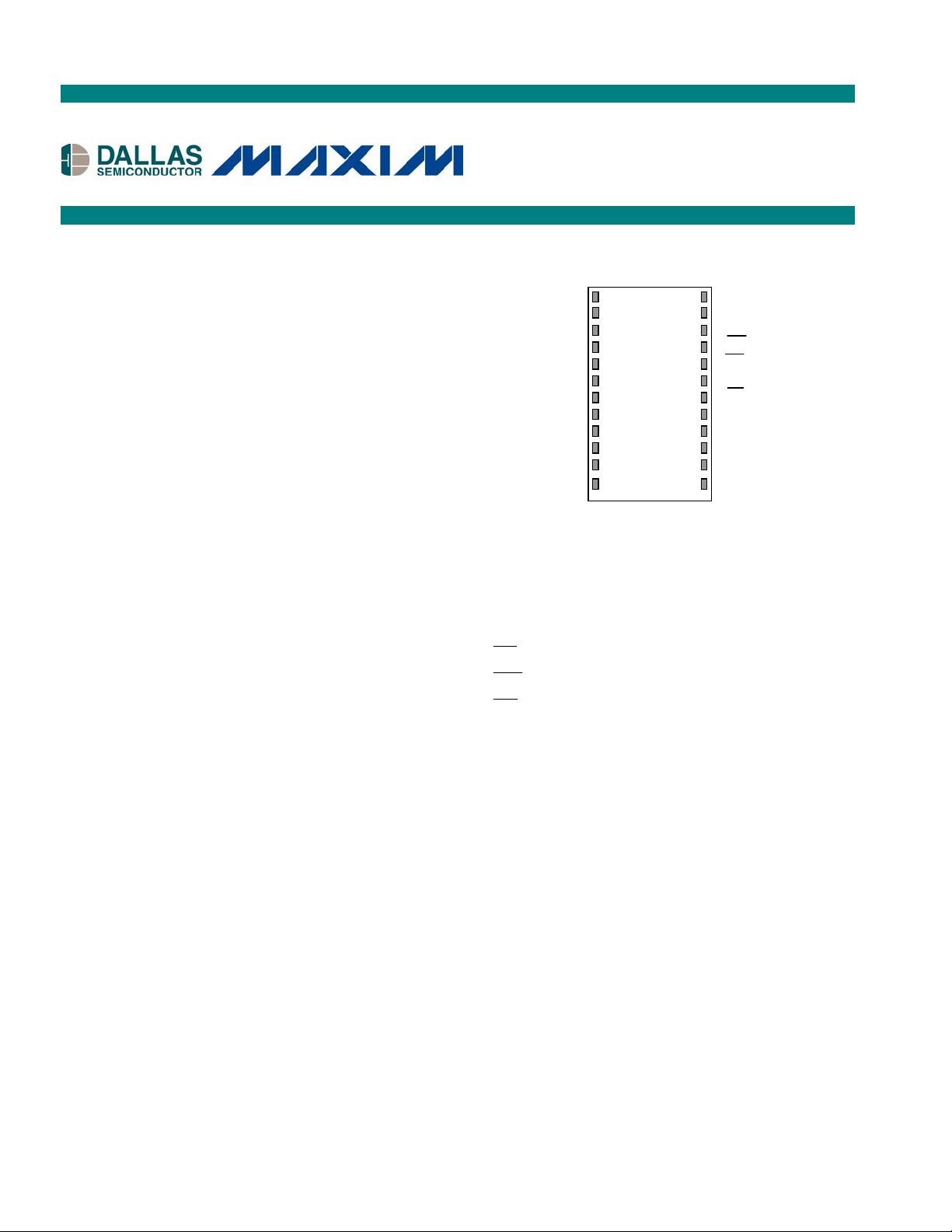
PIN ASSIGNMENT
PIN DESCRIPTION
A0-A10 - Address Inputs
DQ0-DQ7 - Data In/Data Out
A7
A6
A5
A4
A3
A2
A1
A0
DQ0
DQ1
DQ2
GND
1
2
3
4
5
6
7
8
9
10
11
12
24
23
22
21
20
19
18
17
16
15
14
13
VCC
8
9
OE
10
CE
DQ7
DQ6
DQ5
DQ4
DQ3
24-Pin ENCAPSULATED PACKAGE
720-mil EXTENDED
CE - Chip Enable
WE - Write Enable
OE - Output Enable
V
- Power (+5V)
CC
GND - Ground
DESCRIPTION
The DS1220Y 16k Nonvolatile SRAM is a 16,384-bit, fully static, nonvolatile RAM organized as 2048
words by 8 bits. Each NV SRAM has a self-contained lithium energy source and control circuitry which
constantly monitors V
energy source is automatically switched on and write protection is unconditionally enabled to prevent
data corruption. The NV SRAM can be used in place of existing 2k x 8 SRAMs directly conforming to
the popular bytewide 24-pin DIP standard. The DS1220Y also matches the pinout of the 2716 EPROM or
the 2816 EEPROM, allowing direct substitution while enhancing performance. There is no limit on the
number of write cycles that can be executed and no additional support circuitry is required for
microprocessor interfacing.
for an out-of-tolerance condition. When such a condition occurs, the lithium
CC
1 of 8 081506
Page 2

DS1220Y
READ MODE
The DS1220Y executes a read cycle whenever WE (Write Enable) is inactive (high) and CE (Chip
Enable) and
OE (Output Enable) are active (low). The unique address specified by the 11 address inputs
(A0-A10) defines which of the 2048 bytes of data is to be accessed. Valid data will be available to the
eight data output drivers within t
CE and OE access times are also satisfied. If CE and OE access times are not satisfied, then data
that
access must be measured from the later-occurring signal and the limiting parameter is either t
for OE rather than address access.
t
OE
(Access Time) after the last address input signal is stable, providing
ACC
for CE or
CO
WRITE MODE
The DS1220Y executes a write cycle whenever the WE and CE signals are active (low) after address
inputs are stable. The later-occurring falling edge of
cycle. The write cycle is terminated by the earlier rising edge of
kept valid throughout the write cycle.
) before another cycle can be initiated. The OE control signal should be kept inactive (high) during
(t
WR
WE must return to the high state for a minimum recovery time
write cycles to avoid bus contention. However, if the output drivers are enabled (
then
WE will disable the outputs in t
from its falling edge.
ODW
CE or WE will determine the start of the write
CE or WE . All address inputs must be
CE and OE active)
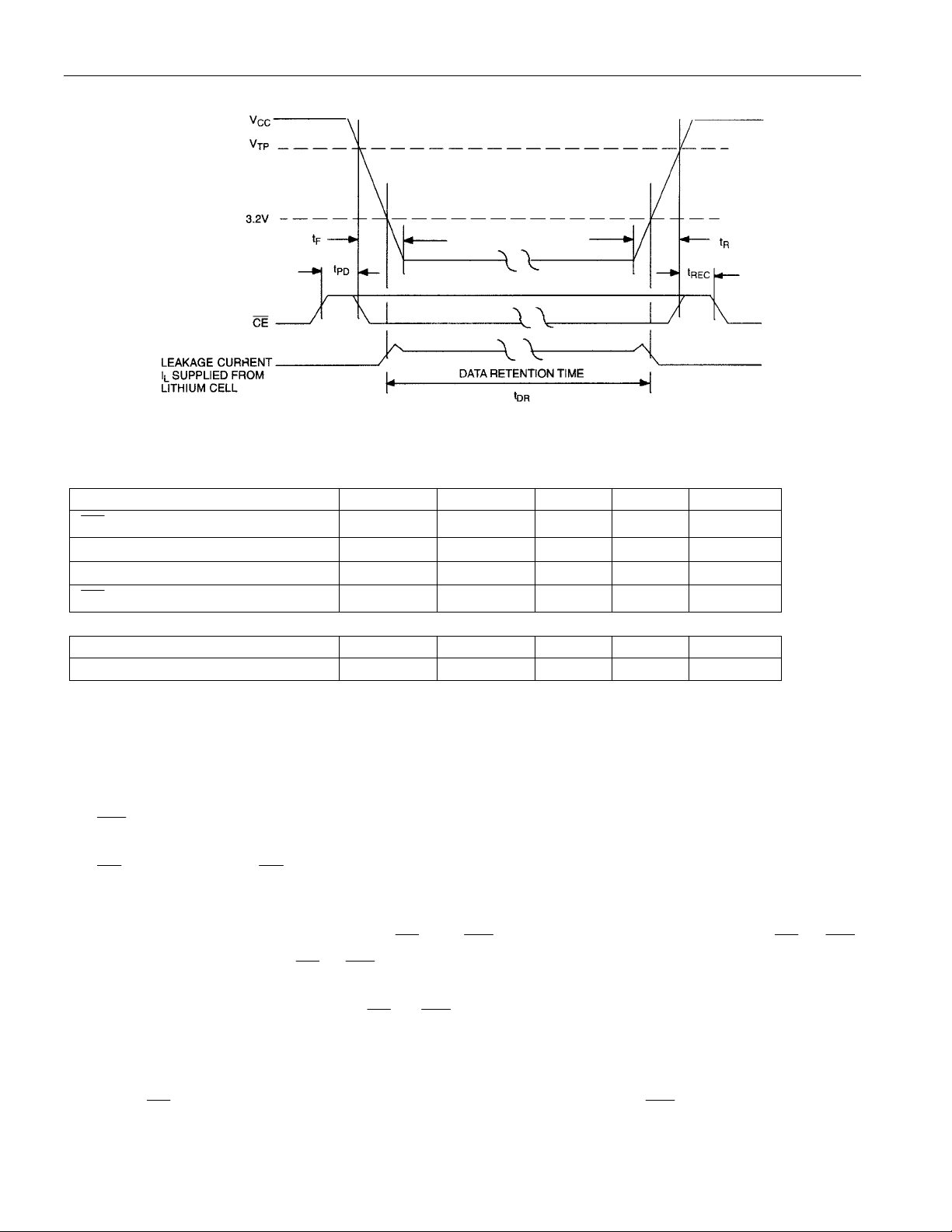
DATA RETENTION MODE
The DS1220Y provides full-functional capability for VCC greater than 4.5 volts and write protects at 4.25
nominal. Data is maintained in the absence of V
DS1220Y constantly monitors V
. Should the supply voltage decay, the NV SRAM automatically write
CC
protects itself, all inputs become “don’t care,” and all outputs become high-impedance. As V
below approximately 3.0 volts, a power switching circuit connects the lithium energy source to RAM to
retain data. During power-up, when V
connects external V
resume after V
CC
to RAM and disconnects the lithium energy source. Normal RAM operation can
CC
exceeds 4.5 volts.
rises above approximately 3.0 volts, the power switching circuit
CC
without any additional support circuitry. The
CC
falls
CC
2 of 8
Page 3
DS1220Y
ABSOLUTE MAXIMUM RATINGS*
Voltage on Any Pin Relative to Ground -0.3V to +7.0V
Operating Temperature 0
Storage Temperature -40
°C to 70°C; -40°C to +85°C for IND parts
°C to +70°C; -40°C to +85°C for IND parts
Soldering Temperature +260°C for 10 seconds
Caution: Do Not Reflow (Wave or Hand Solder Only)
This is a stress rating only and functional operation of the device at these or any other conditions above
those indicated in the operation sections of this specification is not implied. Exposure to absolute
maximum rating conditions for extended periods of time may affect reliability.
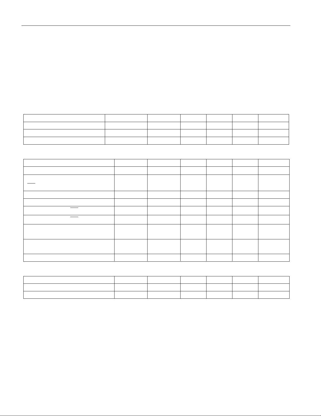
RECOMMENDED DC OPERATING CONDITIONS (TA : See Note 10)
PARAMETER SYMBOL MIN TYP MAX UNITS NOTES
Power Supply Voltage VCC 4.5 5.0 5.5 V
Input Logic 1 VIH 2.2 VCC V
Input Logic 0 VIL 0.0 +0.8 V
DC ELECTRICAL CHARACTERISTICS (TA : See Note 10; VCC = 5V ± 10%)
PARAMETER SYMBOL MIN TYP MAX UNITS NOTES
Input Leakage Current IIL -1.0 +1.0
I/O Leakage Current
CE ³ V
IH
£ V
CC
I
-1.0 +1.0
IO
mA
mA
Output Current @ 2.4V IOH -1.0 mA
Output Current @ 0.4V IOL 2.0 mA
I
3.0 7.0 mA
Standby Current CE =2.2V
Standby Current CE =VCC -0.5V
Operating Current t
= 200ns
CYC
CCS1
I
2.0 4.0 mA
CCS2
I
75 mA
CCO1
(Commercial)
Operating Current t
CYC
=200ns
I
85 mA
CCO1
(Industrial)
Write Protection Voltage VTP 4.25 V
CAPACITANCE (T
A
PARAMETER SYMBOL MIN TYP MAX UNITS NOTES
Input Capacitance CIN 5 10 pF
Input/Output Capacitance C
5 12 pF
I/O
= 25°C)
3 of 8
Page 4
DS1220Y
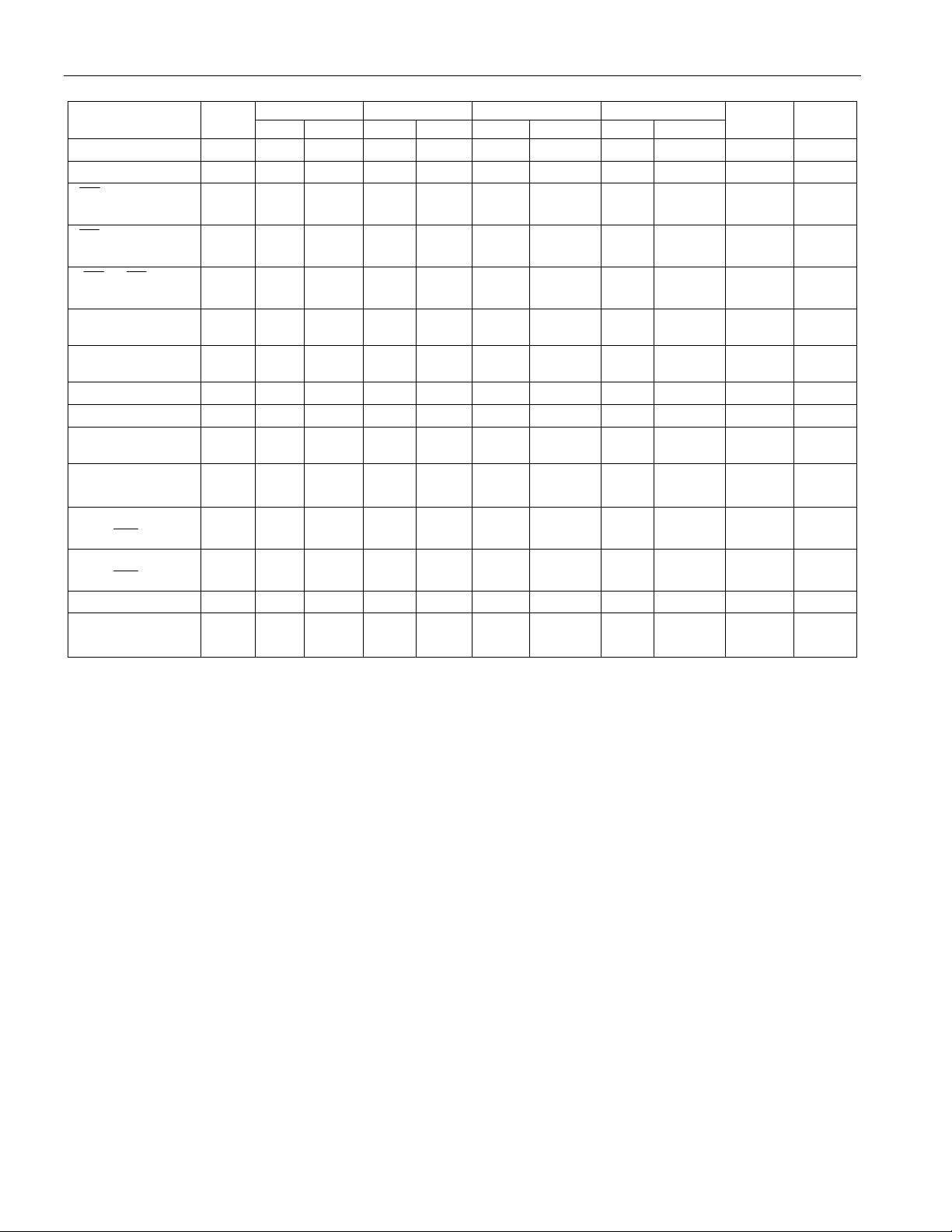
AC ELECTRICAL CHARACTERISTICS (TA : See Note 10; VCC =5.0V ± 10%)
PARAMETER SYM
Read Cycle Time
Access Time
t
OE to Output
Valid
CE to Output
Valid
OE or CE to
Output Active
t
Output High Z
from Deslection
Output Hold from
Address Change
Write Cycle Time
Write Pulse Width
Address Setup
Time
Write Recovery
Time
t
t
t
t
t
Output High Z
t
from
WE
ODW
Output Active
t
from
WE
OEW
Data Setup Time
Data Hold Time
t
t
DS1220Y-100 DS1220Y-120 DS1220Y-150 DS1220Y-200
MIN MAX MIN MAX MIN MAX MIN MAX
t
ACC
t
t
COE
t
t
WC
WP
AW
WR1
WR2
t
DH1
DH2
100 120 150 200 ns
RC
100 120 150 200 ns
50 60 70 100 ns
OE
100 120 150 200 ns
CO
5 5 5 5 ns 5
35 35 35 35 ns 5
OD
5 5 5 5 ns
OH
100 120 150 200 ns
75 90 100 150 ns 3
0 0 0 0 ns
DS
0
10
35 35 35 35 ns 5
5 5 5 5 ns 5
40 50 60 80 ns 4
0
10
0
10
0
10
0
10
0
10
10
10
UNITS NOTE
0
0
ns
ns
ns
ns
12
13
12
13
4 of 8
Page 5
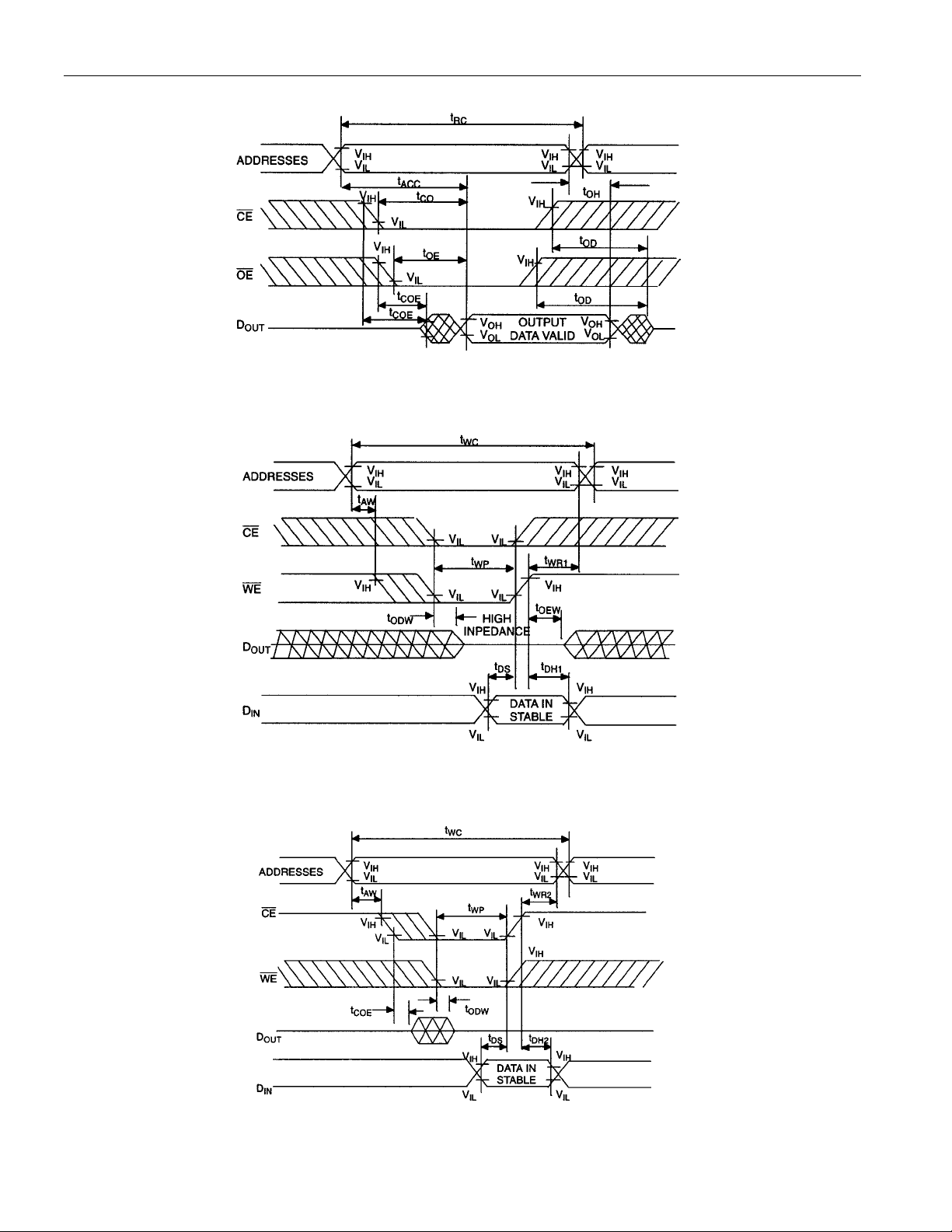
READ CYCLE
DS1220Y
SEE NOTE 1
WRITE CYCLE 1
SEE NOTES 2, 3, 4, 6, 7, 8 AND 12
WRITE CYCLE 2
SEE NOTES 2, 3, 4, 6, 7, 8 AND 13
5 of 8
Page 6
DS1220Y
POWER-DOWN/POWER-UP CONDITION
SEE NOTE 11
POWER-DOWN/POWER-UP TIMING
PARAMETER SYMBOL MIN MAX UNITS NOTES
t
0
CE at V
V
Slew from VTP to 0V tF 100
CC
before Power-Down
IH
VCC Slew from 0V to VTP t
CE at VIH after Power-Up
PD
0
R
t
2 ms
REC
ms
ms
ms
11
(TA = 25°C)
PARAMETER SYMBOL MIN MAX UNITS NOTES
Expected Data Retention Time tDR 10 years 9
WARNING:
Under no circumstance are negative undershoots, of any amplitude, allowed when device is in battery
backup mode.
NOTES:
1. WE is high for a read cycle.
2.
OE = VIH or VIL . If OE = VIH during a write cycle, the output buffers remain in a high impedance
state.
3. t
is specified as the logical AND of CE and WE . tWP is measured from the latter of CE or WE
WP
going low to the earlier of
CE or WE going high.
4. t
are measured from the earlier of CE or WE going high.
DS
5. These parameters are sampled with a 5 pF load and are not 100% tested.
6. If the
CE low transition occurs simultaneously with or later than the WE low transition in write
cycle 1, the output buffers remain in a high impedance state during this period.
6 of 8
Page 7
DS1220Y
7. If the
CE high transition occurs prior to or simultaneously with the WE high transition, the output
buffers remain in a high impedance state during this period.
8. If
WE is low or the WE low transition occurs prior to or simultaneously with the CE low transition,
the output buffers remain in a high impedance state during this period.
9. Each DS1220Y is marked with a 4-digit date code AABB. AA designates the year of manufacture.
BB designates the week of manufacture. The expected t
is defined as starting at the date of
DR
manufacture.
10. All AC and DC electrical characteristics are valid over the full operating temperature range. For
commercial products, this range is 0°C to 70°C. For industrial products (IND), this range is -40°C to
+85°C.
11. In a power-down condition the voltage on any pin may not exceed the voltage of V
CC
.
12. t
WR1
, t
are measured from WE going high.
DH1
13. t
WR2
, t
are measured from CE going high.
DH2
14. DS1220Y modules are recognized by Underwriters Laboratory (U.L.
DC TEST CONDITIONS
Outputs open.
All voltages are referenced to ground.
AC TEST CONDITIONS
Output Load: 100pF + 1TTL Gate
Input Pulse Levels: 0-3.0V
Timing Measurement Reference Levels
Ò) under file E99151 (R).
Input:1.5V
Output: 1.5V
Input Pulse Rise and Fall Times: 5ns
ORDERING INFORMATION
PART NUMBER
DS1220Y-100 0°C to +70°C
DS1220Y-100+ 0°C to +70°C
DS1220Y-100IND -40°C to +85°C
DS1220Y-100IND+ -40°C to +85°C
DS1220Y-120 0°C to +70°C
DS1220Y-120+ 0°C to +70°C
DS1220Y-150 0°C to +70°C
DS1220Y-150+ 0°C to +70°C
DS1220Y-200 0°C to +70°C
DS1220Y-200+ 0°C to +70°C
DS1220Y-200IND -40°C to +85°C
DS1220Y-200IND+ -40°C to +85°C
+ Denotes lead-free/RoHS-compliant product.
TEMPERATURE
RANGE
SUPPLY
TOLERANCE
5V ± 10%
5V ± 10%
5V ± 10%
5V ± 10%
5V ± 10%
5V ± 10%
5V ± 10%
5V ± 10%
5V ± 10%
5V ± 10%
5V ± 10%
5V ± 10%
PIN/PACKAGE
24 / 720 EMOD 100ns
24 / 720 EMOD 100ns
24 / 720 EMOD 100ns
24 / 720 EMOD 100ns
24 / 720 EMOD 120ns
24 / 720 EMOD 120ns
24 / 720 EMOD 150ns
24 / 720 EMOD 150ns
24 / 720 EMOD 200ns
24 / 720 EMOD 200ns
24 / 720 EMOD 200ns
24 / 720 EMOD 200ns
SPEED
GRADE
7 of 8
Page 8

DS1220Y NONVOLATILE SRAM, 24-PIN 720-MIL EXTENDED MODULE
PKG 24-PIN
DIM MIN MAX
A IN.
MM
B IN.
MM
C IN.
MM
D IN.
MM
E IN.
MM
F IN.
MM
G IN.
MM
H IN
MM
J IN.
MM
K IN.
MM
1.320
33.53
0.695
17.65
0.390
9.91
0.100
2.54
0.017
0.43
0.120
3.05
0.090
2.29
0.590
14.99
0.008
0.20
0.015
0.38
1.340
34.04
0.720
18.29
0.415
10.54
0.130
3.30
0.030
0.76
0.160
4.06
0.110
2.79
0.630
16.00
0.012
0.30
0.021
0.53
DS1220Y
8 of 8
 Loading...