

Page 1
CE
WE
OE
DS1220AB/AD
19-5580; Rev 10/10
www.maxim-ic.com
14
VCC
1 2 3 4 5 6 7
8 9 10
11
12
13
24
15
23
22
21
20
19
18
17
16
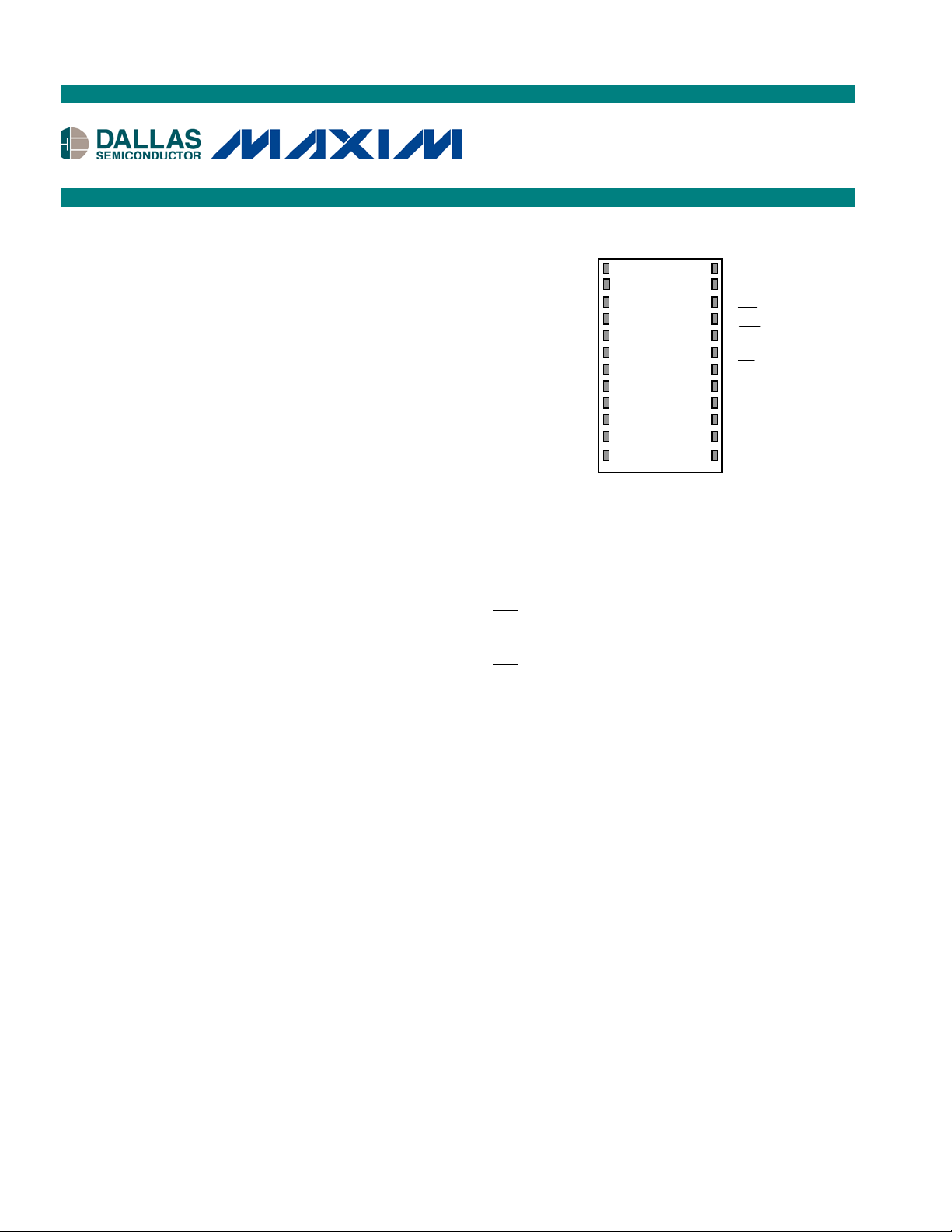
A7 A5 A3
A2
A1
A0
DQ0
DQ1
GND
DQ2 A6
A4
A8
A9
OE
A10
CE
DQ7
DQ6
DQ5
DQ3
DQ4
FEATURES
10 years minimum data r etent ion in the
absence of external power
Data is automatically pro tected during power
loss
Directly replaces 2k x 8 volatile static RAM
or EE P R O M
Unlimited write c ycles
Low-power CMOS
JEDEC standard 24-pin DIP packag e
Read and write access times of 100 ns
Lithium energy sour ce is electrically
disconnected to retain freshness until power
is applied for the first time
Full ±10% VCC operating range (DS1220AD)
Optional ±5% VCC operating range
(DS1220AB)
Optional industrial temperature range of
-40°C to +85°C, designated IND
16k Nonvolatile SRAM
PIN ASSIGNMENT
24-Pin ENCAPSULATED PACKAGE
720-mil EXTENDED
PIN DESCRIPTION
A0-A10 - Address Inputs
DQ0-DQ7 - Data In/Data Out
- Chip Enable
- Write Enable
- Output Enable
V
- Power (+5V)
CC
GND - Ground
DESCRIPTION
The DS1220AB and DS1220AD 16k Nonvolatile SRAMs are 16,384-bit, fully st atic, nonvolatile SRAMs
organized as 2048 words by 8 bits. Each NV SRAM has a self-contained lithium energy source and
cont r ol c ircuit ry w h i ch c onsta n tly mon ito r s VCC fo r a n o ut-of-to ler a nc e c o nditio n. Whe n s uc h a c o nd ition
occurs, the lithium energy source is automatically switched on and write prot ection is uncond itionally
enabled to prevent data corruption. The NV SRAMs can be used in place of existing 2k x 8 SRAMs
directly conforming to the popular bytewide 24-pin DIP standard. The devices also match the pinout of
the 2716 EPROM and the 2816 EEPROM, allowing direct substitution while enhancing performance.
There is no limit o n t he number of write cycles that can be execut ed and no additional support circuitry is
required for microp ro cessor interfacing.
1 of 8
Page 2

2 of 8
READ MODE
WE
CE
OE
OE
WE
WE
WE
WE
OE
OE
WE
DS1220AB/AD
The DS1220AB and DS1220AD execute a read cycle whenever
(Write Enable) is inact ive (high) and
(Chip Enable) and OE(Output Enable) are active (low). The unique address specified by the 11
address inputs (A0-A10) defines which of the 2048 bytes o f data is to be accessed. Valid data w ill be
available to the eight data output drivers within t
stable, providing that the CEand
access t imes are also sat isfied. If CEand
(Access T ime) after the last address input signal is
ACC
access times are not
satisfied, then data access must be measured fro m the later-oc cu rr ing s ig na l a nd t he li miting p ar a meter is
either tCO for CEor tOE for OE rather than address access.
WRITE MODE
The DS1220AB and DS1220AD execute a write cycle whenever the
after address inputs are stable. T he latt er occurring falling edge of CEor
the write cycle. Th e write cycle is terminated b y the earlier r ising edge o f CEor
must be kept va lid t hro ug ho ut the wr it e c ycle.
time ( tWR ) before a not her cycle can be in itiated. The
must return to the high state for a minimum recovery
co ntrol sig nal s hould be kept inact ive (hig h)
during write cycles to avoid bus contention. However, if the output drivers are enabled (CEand
active) then
will disable the o utputs in t
from its falling edge.
ODW
and CE signals are act ive (low)
will de ter mine t he start of
. All address inputs
DATA RETENTION MODE
The DS1220AB provides full functional capability for V
4.5V. The DS1220AD provides full functional capability for VCC greater than 4.5 volts and write protects
by 4.25V. Data is maintained in the absence of VCC without any additional support circuitry. The
nonvolatile static RAMs constantly monitor VCC. Should the supply voltage decay, the NV SRAMs
automatically write protect themselves, all inputs become “don’t care,” and all outputs become high
impedance. As VCC falls below approximately 3.0 volts, a power sw itching circu it co nnects the lithiu m
energy source to RAM to r etain data. During power-up , when VCC rises above approximately 3.0 volts,
the power sw itching c ircuit connect s external VCC to RAM and disconnects the lithium energy source.
Normal RAM operat ion can resu me after VCC exceeds 4.75 volts for the DS1220AB and 4.5 volts for the
DS1220AD.
greater t han 4.75 volts and wr ite protect s by
CC
FRESHNESS SEAL
Each DS1220 device is shipped from Dallas Semiconductor with its lithium energy source disconnected,
guaranteeing fu ll energ y capac it y. When VCC is first app lied at a level o f greater t han VTP, t he lithi um
energy source is enabled for battery backup operation.
Page 3
DS1220AB/AD
3 of 8
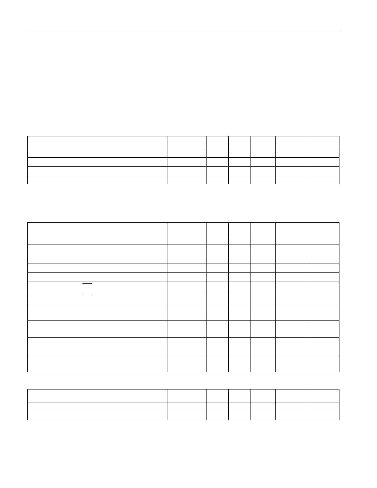
DS1220AB Power Supply Voltage
VCC
4.75
5.0
5.25
V
DS1220AD Power Supply Voltage
VCC
4.50
5.0
5.50
V
Log ic 1
VIH
2.2 VCC
V
Log ic 0
VIL
0.0 +0.8
V
Input Leakage Current
IIL
-1.0
+1.0
µA
I/O Leakage Current
CE
-1.0
Output Current @ 2.4V
IOH
-1.0
mA
Output Current @ 0.4V
IOL
2.0
mA
CE
Standby Current
CE
VCC-0.5V
Operating Current
(Commercial)
Operating Current
(Industrial)
Write Protection Voltage
(DS1220AB)
Write Protection Voltage
Input Capacitance
CIN
5 10
pF
Input/O utput Capacitanc e
C
I/O
5 12
pF
ABSOLUTE MAXIMUM RATINGS
Voltage on Any Pin Relative to Ground -0.3V to +6.0V
Operating Temperat ur e Range
Commercial: 0°C to +70°C
Industrial: -40°C to +85°C
Storage Temperatu r e -40°C to +85°C
Lead Temperature (soldering, 10s) +260°C
Note: EDIP is wave or hand soldered only.
This is a stress rating only and functional operation of the device at these or any other conditions above those indicated in the operation sections of this
specification is not i mplied. Exposure to absolute m ax imum rating condition s for extended periods of tim e may affect reliability.
RECOMMENDED DC OPERATING CONDITIONS (TA: See Note 10)
PARAMETER SYMBOL MIN TYP MAX UNITS NOTES
DC ELECTRICAL CHARACTERISTICS (TA: See Note 10)
(V
= 5V ± 5% for DS1220AB)
CC
(V
= 5V ± 10% for DS1220AD)
CC
PARAMETER SYMBOL MIN TYP MAX UNITS NOTES
≥ V
≤ VCC
IH
Standby Current
= 2.2V
=
I
CCS1
I
CCS2
I
CC01
I
CCO1
IO
+1.0
µA
5.0 10.0 mA
3.0 5.0 mA
75 mA
85 mA
I
VTP 4.5 4.62 4.75 V
(DS1220AD)
VTP 4.25 4.37 4.5 V
CAPACITANCE (TA = +25°C)
PARAMETER SYMBOL MIN TYP MAX UNITS NOTES
Page 4

4 of 8
AC ELECTRICAL CHARACTERISTICS (T
DS1220AB-100
DS1220AD-100
MIN
MAX
Read Cycle Time
tRC
100 ns
Acce ss Time
t
ACC
100
ns
OE
to Output Valid
CE
to Output Valid
CE
to Output Active
Output Hig h Z fr om
Output Hold from Address Change
tOH
5 ns
Writ e Cycle Time
tWC
100 ns
Write Pulse Width
tWP
75 ns
3
Address Setup Time
tAW
0 ns
t
t
WR2
0
10
ns
ns
12
13
Output Hig h from
WE
WE
Data Setup Time
tDS
40 ns
4
t
t
DH2
0
10
ns
ns
12
13
(V
= 5.0V ± 5% for DS1220AB)
CC
(V
= 5.0V ± 10% for DS1220AD)
CC
DS1220AB/AD
: See Note 10)
A
PARAMETER SYMBOL
OE or
Deselection
Write Recovery Time
Output Active from
Data Hold Time
tOE 50 ns
tCO 100 ns
t
5 ns 5
COE
tOD 35 ns 5
WR1
t
35 ns 5
ODW
t
5 ns 4
OEW
DH1
UNITS NOTES
Page 5

5 of 8
READ CYCLE
DS1220AB/AD
SEE NOTE 1
WRITE CYCLE 1
SEE NOTES 2, 3, 4, 6, 7, 8 AND 12
WRITE CYCLE 2
SEE NOTES 2, 3, 4, 6, 7, 8 AND 13
Page 6

6 of 8
POWER-DOWN/POWER-UP CONDITION
WE
WE
Expected Dat a Retent ion T ime
tDR
10
years
9
WE
OE
OE
WE
CE
WE
WE
WE
WE
DS1220AB/AD
SEE NOTE 11
POWER-DOWN/POWER-UP TIMING (TA: See Note 10)
PARAMETER SYMBOL MIN TYP MAX UNITS NOTES
VCC Fail Detect to CE and
Inactive
VCC s lew from VTP to 0V t
VCC slew from 0V to VTP t
VCC Va lid to CE and
Inactive
VCC Valid to End of Write Protection t
t
PD
F
R
t
PU
REC
1.5
300
300
µs
µs
µs
2 ms
125 ms
11
(TA = +25°C)
PARAMETER SYMBOL MIN TYP MAX UNITS NOTES
WARNING:
Under no circumstances are negative undershoots, of any amplitude, allowed when device is in the
battery backup mode.
NOTES:
1.
2.
is high for a read cycle.
= V
or VIL. If
IH
3. tWP is spec ified as t he log ical AND o f CEand
going low to the earlier of CE or
4. tDS is m e asured from the earlier of CE or
5. These parameters ar e sa mpled with a 5 pF load and ar e not 100% t ested .
6. If t he CE low transition occurs simultaneo usly with or later t han the
buffe rs remain in a high-impedance state during this period.
7. If t he CE hig h t ra ns it io n o cc ur s pr io r t o or s imu lt a ne o us ly w it h th e
buffers re main in a high-impedance state during this period.
= VIH during write cycle, the output buffers remain in a high-impedance state.
. tWP is measured from the latt er of CE or
going h igh.
going high.
low t rans itio n, t he o utp ut
hig h tr ansit io n, t he ou tp ut
Page 7
DS1220AB/AD
7 of 8
WE
WE
SUPPLY
TOLERANCE
DS1220AB-100+
0°C to +70°C
24 720 EDIP
DS1220AB-100IND+
-40°C to +85°C
5V ± 5%
24 720 EDIP
DS1220AD-100+
0°C to +70°C
5V ± 10%
24 720 EDIP
DS1220AD-100IND+
-40°C to +85°C
5V ± 10%
24 720 EDIP
LAND
PATTERN NO.
8. If
is low or th e
low transition occurs prior to or simultaneously with the CE low t r ans ition,
the output buffers re m ain in a high-impedance state during this period.
9. Each DS1220AB and each DS1220AD has a built-in switch t hat d isconnects the lithium sour ce unt il
VCC is first app lied by the u ser. The expected tDR is defined as accumu lative time in the absence o f
VCC s ta rt ing fro m the t ime power is first applied by the user. This parameter is guaranteed by design
and is not 100% tested.
10. All AC and DC electrical characteristics are valid over the full operating temperature range. For
commercial products, this range is 0°C to 70°C. For industrial product s (IND), this range is -40°C to
+85°C.
11. In a power down co ndition the voltage on an y pin ma y not exceed the voltage on VCC.
12. t
13. t
WR1
WR2
, t
are measured from
DH1
, t
are measured from CEgoing h igh.
DH2
WE
going high.
14. DS1220 modules are recognized by Underwriters Laboratories (UL) under file E99151.
DC TEST CONDITIONS
Outputs Open
Cycle = 200ns for Operating Current
All Voltages Are Referenced t o Ground
AC TEST CONDITIONS
Output Load: 100 pF + 1TTL Gate
Input Pulse Levels: 0 - 3.0V
Timing Measurement Reference Levels
Input: 1.5V
Output: 1.5V
Input Pulse Rise and Fall Times: 5ns
ORDERING INFORMATION
PART TEMP RANGE
PIN-PACKAGE
5V ± 5%
+Denotes a lead(Pb)-free/RoHS-compliant package.
PACKAGE INFORMATION
For the latest package outline informat ion and land patterns, go to www.maxim-ic.com/packages. Note
that a “+”, “#”, or “-” in t he package cod e indicat es RoHS statu s only. Package drawings may show a
different suffix charact er, but the drawing pertains to the package regardless of RoHS status.
PACKAGE TYPE PACKAGE CODE OUTLINE NO.
24 EDIP MDT24+1
21-0245
 Loading...