

Page 1
General Description
The DS1123L is an 8-bit programmable timing element
similar in function to the DS1023, but operating at 3.3V.
Like the DS1023, the DS1123L can delay signals up to
a full period or more when used as a delay line, and an
on-chip reference delay can be used to offset the inherent “step-zero” delay. This allows the DS1123L to shift a
clock signal over the full 0 to 360° phase range. In
addition to functioning as a delay line, it can be configured as a free-running oscillator or an externally triggered monostable vibrator.
Applications
Telecommunications
Digital Test Equipment
Digital Video Projection
Signal Generators and Analyzers
Features
♦ Step Sizes of 0.25ns, 0.5ns, 1ns, 2ns
♦ On-Chip Reference Delay
♦ Configurable as a Delay Line, Monostable
Vibrator, or Free-Running Oscillator
♦ Can Delay Signals by a Full Period or More
♦ Guaranteed Monotonicity
♦ Parallel and 3-Wire Serial Programming Interface
♦ Single 3.3V Power Supply
♦ 16-pin TSSOP
DS1123L
3.3V, 8-Bit, Programmable Timing Element
_____________________________________________
Maxim Integrated Products
1
15
14
13
12
11
10
9
2
161
3
4
5
6
7
8
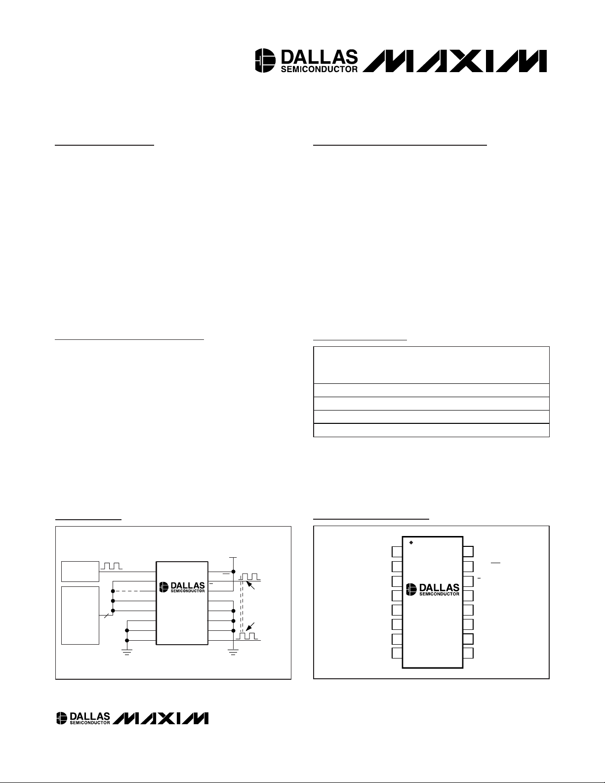
OUT/OUT
P/S
P7
P6P2/D
P1/CLK
P0/Q
LE
V
CC
IN
TOP VIEW
MS
P5
REF/PWMGND
P4
P3
DS1123L
Pin Configuration
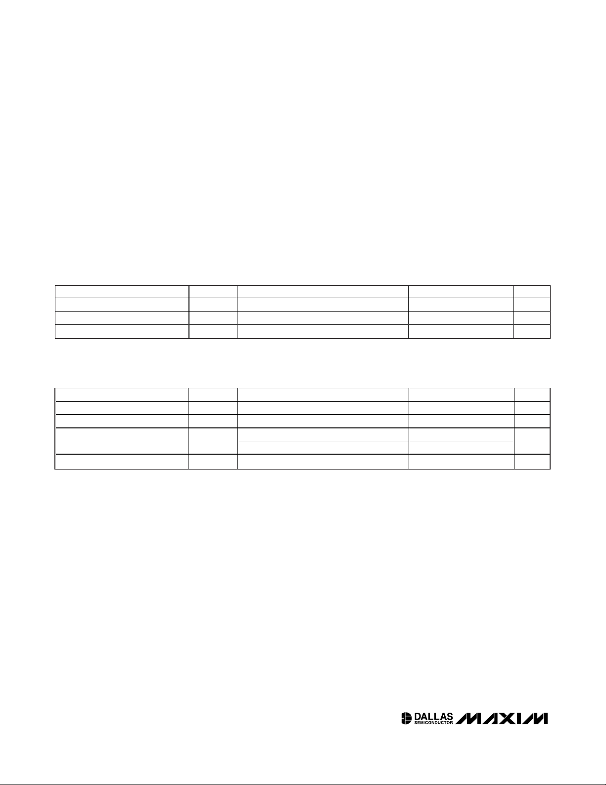
DS1123L
SYSTEM
CLOCK
MICRO-
PROCESSOR
4
3-WIRE
INTERFACE
IN
Q/P0
CLK/P1
D/P2
P3
P4
LE
P5
MS
P6
P7
P/S
OUT/OUT
V
CC
GND REF/PWM
3.3V
VARIABLE
DELAY/PHASE
OUTPUT
REFERENCE
OUTPUT
(OPTIONAL)
Typical Operating Circuit
Ordering Information
Rev 2; 8/07
For pricing, delivery, and ordering information, please contact Maxim Direct at 1-888-629-4642,
or visit Maxim’s website at www.maxim-ic.com.
PART
TEMP
RANGE
PINPACKAGE
(150-mil)
STEP SIZE/
NO. OF STEPS
DS1123LE-25
0.25/256
DS1123LE-50
0.5/256
DS1123LE-100
1/256
DS1123LE-200
2/256
0°C to +70°C 16 TSSOP
0°C to +70°C 16 TSSOP
0°C to +70°C 16 TSSOP
0°C to +70°C 16 TSSOP
Page 2
DS1123L
3.3V, 8-Bit, Programmable Timing Element
2 ______________________________________________________________________
ABSOLUTE MAXIMUM RATINGS
RECOMMENDED DC OPERATING CONDITIONS
(TA= 0°C to +70°C)
Stresses beyond those listed under “Absolute Maximum Ratings” may cause permanent damage to the device. These are stress ratings only, and functional
operation of the device at these or any other conditions beyond those indicated in the operational sections of the specifications is not implied. Exposure to
absolute maximum rating conditions for extended periods may affect device reliability.
Voltage Range on VCCPin Relative to Ground .....-0.5V to +6.0V
*Voltage Range on IN, LE, Q/P0, CLK/P1, D/P2, P3, P4, P5, MS,
P6, P7, and P/S Relative to Ground..........-0.5V to V
CC
+ 0.5V
Operating Temperature Range...............................0°C to +70°C
Storage Temperature Range .............................-55°C to +125°C
Short-Circuit Output Current .....................................50mA for 1s
Soldering Temperature .......................................See IPC/JEDEC
J-STD-020A Specification
*Not to exceed +6.0V
DC ELECTRICAL CHARACTERISTICS
(VCC= +3.0 to 3.6V, TA= 0°C to +70°C.)
Supply Voltage V
Input Logic 1 V
Input Logic 0 V
PARAMETER SYMBOL CONDITIONS MIN TYP MAX UNITS
CC
(Note 1) +3.0 +3.6 V
(Note 2) 0.7 x V
IH
IL
Active and Standby Current I
High-Level Output Current I
Low-Level Output Current I
Input Leakage I
PARAMETER SYMBOL CONDITIONS MIN TYP MAX UNITS
CC
V
OH
OL
L
= min, V
CC
Q output, V
All other outputs, V
V
CC
-0.3 +0.3 x V
16 30 mA
= 2.3V -1.0 mA
OH
CC
= min, V
= 0.5V 4.0
OL
CC
= min, V
= 0.5V 8.0
OL
-1.0 +1.0 µA
+ 0.3 V
CC
CC
V
mA
Page 3
DS1123L
3.3V, 8-Bit, Programmable Timing Element
_____________________________________________________________________ 3
AC ELECTRICAL CHARACTERISTICS (ALL SPEED OPTIONS)
(VCC= +3.0V to 3.6V, TA= 0°C to +70°C.)
Serial Clock Frequency f
Input Pulse Width (LE, CLK) T
Data Setup to Clock t
Data Hold from Clock t
Data Setup to Enable t
Data Hold to Enable t
Enable Setup to Clock t
Enable Hold from Clock t
LE to Q Valid t
LE to Q High-Z t
CLK to Q Valid t
CLK to Q Invalid t
Parallel Input to Delay Valid t
Parallel Input to Delay Invalid t
LE to Delay Valid t
LE to Delay Invalid t
Power-Up Time t
PARAMETER SYMBOL CONDITIONS MIN TYP MAX UNITS
CLK
W
DSC
DHC
DSE
DHE
ES
EH
EQV
EQZ
CQV
CQX
PDV
PDX
EDV
EDX
PU
10 MHz
50 ns
30 ns
0ns
30 ns
0ns
0ns
30 ns
50 ns
050ns
50 ns
0ns
500 ns
0ns
500 ns
0ns
100 ms
Page 4
DS1123L
3.3V, 8-Bit, Programmable Timing Element
4 ______________________________________________________________________
AC ELECTRICAL CHARACTERISTICS (DS1123L-25)
(VCC= +3.0V to 3.6V, TA= 0°C to +70°C.)
Reference Delay t
Delay Step Size t
Step-Zero Delay with Respect
to IN
Step-Zero Delay with Respect
to REF
Maximum Delay with Respect
to IN
Delay with Respect to REF t
Delay with Respect to REF
Tolerance
Voltage Delay Variation (Notes 7, 9) -1 +1 %
Temperature Delay Variation VCC = 3.3V (Notes 7, 9) -2.5 +2.5 %
Integral Nonlinearity (Deviation
from Straight Line)
OUT Delta Delay t
IN High to PWM High t
Minimum PWM Output Pulse
Width
Minimum Input Pulse Width t
Minimum Input Period (Note 15) 80 ns
Input Rise and Fall Times tr, t
PARAMETER SYMBOL CONDITIONS MIN TYP MAX UNITS
REF
STEP
t
D0
t
D0REF
t
DMAX
DREF
Δt
DREF
t
DREF
Δt
DV
t
DREF
Δt
DT
t
DREF
t
err
INV0
PWM0
t
PWM
WI
(Notes 3, 4) 18 22 ns
TA = +25°C 0 0.25 1.75 ns
(Notes 4, 5) 16.5 22 ns
(Notes 6, 7) -2.5 -1.5 0 ns
(Notes 4, 8) 80 ns
Position FO (Notes 7, 9) 60 ns
VCC = 3.3V, TA = +25°C
(Notes 7, 9)
(Note 10) -2 0 +2 ns
(Note 11) 0 1 2.5 ns
(Notes 4, 12) 16.5 22 ns
(Note 13) 5 ns
(Note 14) 40 ns
(Note 16) 0 1 µs
f
-0.75 +0.75 %
Page 5
DS1123L
3.3V, 8-Bit, Programmable Timing Element
_____________________________________________________________________ 5
AC ELECTRICAL CHARACTERISTICS (DS1123L-50)
(VCC= +3.0V to 3.6V, TA= 0°C to +70°C.)
PARAMETER SYMBOL CONDITIONS MIN TYP MAX UNITS
Reference Delay t
Delay Step Size t
Step-Zero Delay with Respect
to IN
Step-Zero Delay with Respect
to REF
Maximum Delay with Respect
to IN
Delay with Respect to REF t
Delay with Respect to REF
Tolerance
Voltage Delay Variation (Notes 7, 9) -0.75 +0.75 %
Temperature Delay Variation VCC = 3.3V (Notes 7, 9) -2.5 +2.5 %
Integral Nonlinearity (Deviation
from Straight Line)
OUT Delta Delay t
IN High to PWM High t
Minimum PWM Output Pulse
Width
Minimum Input Pulse Width t
Minimum Input Period (Note 15) 80 ns
Input Rise and Fall Times tr, t
REF
STEP
t
D0
t
D0REF
t
DMAX
DREF
Δt
DREF
t
DREF
Δt
DV
t
DREF
Δt
t
DREF
t
err
INV0
PWM0
t
PWM
WI
(Notes 3, 4) 18 22 ns
TA = +25°C
(Notes 4, 5) 16.5 22 ns
(Notes 6, 7) -2.5 -1.5 0 ns
(Notes 4, 8) 144 ns
Position FF (Notes 7, 9) 127.5 ns
VCC = 3.3V, TA = +25°C
(Notes 7, 9)
DT
(Note 10) -2 0 +2 ns
(Note 11) 0 1 2.5 ns
(Notes 4, 12) 16.5 22 ns
(Note 13) 5 ns
(Note 14) 40 ns
(Note 16) 0 1 µs
f
0 0.5 1.75 ns
-0.75 +0.75 %
Page 6

DS1123L
3.3V, 8-Bit, Programmable Timing Element
6 ______________________________________________________________________
AC ELECTRICAL CHARACTERISTICS (DS1123L-100)
(VCC= +3.0V to 3.6V, TA= 0°C to +70°C.)
Note 1: All voltages are referenced to ground.
Note 2: If IN is high during power-up, the output remains low until IN is toggled low and back high again.
Note 3: The reference delay is closely matched to the step-zero delay to allow relative timings down to zero or less.
Note 4: Measured from rising edge of the input to the rising edge of the output (t
DR
).
Note 5: Delay from input to output with a programmed delay value of zero.
Note 6: This is the relative delay between REF and OUT. The device is designed such that when programmed to zero delay the
OUT output always appears before the REF output. This parameter is numerically equal to t
D0
- t
REF
(see Figure 8).
Note 7: From rising edge to rising edge.
Note 8: This is the actual measured delay from IN to OUT. This parameter exhibits greater temperature variation than the relative
delay parameter.
Note 9: This is the actual measured delay with respect to the REF output. This parameter more closely reflects the programmed
delay value than the absolute delay parameter (see Figure 8). Typical delay shift due to aging is within ±0.85%. Aging
stressing includes level 1 moisture reflow preconditioning (24hr +125°C bake, 168hr +85°C/85%RH moisture soak, and
three solder reflow passes +260°C +0°C/-5°C peak) followed by 1000hr (max) V
CC
biased +125°C OP/L, 1000hr unbi-
ased +150°C bake, and 1000 temperature cycles at -55°C to +125°C.
Reference Delay t
Delay Step Size t
Step-Zero Delay with Respect
to IN
Step-Zero Delay with Respect
to REF
Maximum Delay with Respect
to IN
Delay with Respect to REF t
Delay with Respect to REF
Tolerance
Voltage Delay Variation (Notes 7, 9) -0.5 +0.5 %
Temperature Delay Variation VCC = 3.3V (Notes 7, 9) -2.5 +2.5 %
Integral Nonlinearity (Deviation
from Straight Line)
OUT Delta Delay t
IN High to PWM High t
Minimum PWM Output Pulse
Width
Minimum Input Pulse Width t
Minimum Input Period (Note 15) 80 ns
Input Rise and Fall Times tr, t
PARAMETER SYMBOL CONDITIONS MIN TYP MAX UNITS
REF
STEP
t
D0
t
D0REF
t
DMAX
DREF
Δt
DREF
t
DREF
Δt
DV
t
DREF
Δt
t
DREF
t
err
INV0
PWM0
t
PWM
WI
(Notes 3, 4) 18 22 ns
TA = +25°C 0 1 2.25 ns
(Notes 4, 5) 16.5 22 ns
(Notes 6, 7) -2.5 -1.5 0 ns
(Notes 4, 8) 272 ns
Position FF (Notes 7, 9) 255 ns
VCC = 3.3V, TA = +25°C
(Notes 7, 9)
DT
(Note 10) -4 0 +4 ns
(Note 11) 0 1 2.5 ns
(Notes 4, 12) 16.5 22 ns
(Note 13) 5 ns
(Note 14) 40 ns
(Note 16) 0 1 µs
f
-0.75 +0.75 %
Page 7

DS1123L
3.3V, 8-Bit, Programmable Timing Element
_____________________________________________________________________ 7
AC ELECTRICAL CHARACTERISTICS (DS1123L-200)
(VCC= +3.0V to 3.6V, TA= 0°C to +70°C.)
Note 10: See the
Integral Nonlinearity
section and Figure 9.
Note 11: Change in delay value when the inverted output is selected instead of the normal, noninverting output.
Note 12: In PWM mode, the delay between the rising edge of the input and the rising edge of the output.
Note 13: The minimum value for which the monostable-vibrator pulse width should be programmed. Narrower pulse widths can be
programmed, but output levels may be impaired and ultimately no output pulse is produced.
Note 14: This is the minimum allowable interval between transitions on the input to assure accurate device operation. This parame-
ter may be violated, but timing accuracy may be impaired and ultimately very narrow pulse widths result in no output from
the device.
Note 15: This parameter applies to normal delay mode only. When a 50% duty cycle input clock is used this defines the highest
usable clock frequency. When asymmetrical clock inputs are used, the maximum usable clock frequency must be
reduced to conform to the minimum input pulse-width requirement. In PWM mode, the minimum input period is equal to
the step-zero delay and the programmed delay (t
DO+tD
).
Note 16: Faster rise and fall times give the greatest accuracy in measured delay. Slow edges (outside the specification maximum)
can result in erratic operations.
Reference Delay t
Delay Step Size t
Step-Zero Delay with Respect
to IN
Step-Zero Delay with Respect
to REF
Maximum Delay with Respect
to IN
Delay with Respect to REF t
Delay with Respect to REF
Tolerance
Voltage Delay Variation (Notes 7, 9) -0.5 +0.5 %
Temperature Delay Variation VCC = 3.3V -2.5 +2.5 %
Integral Nonlinearity (Deviation
from Straight Line)
OUT Delta Delay t
IN High to PWM High t
Minimum PWM Output Pulse
Width
Minimum Input Pulse Width t
Minimum Input Period (Note 15) 80 ns
Input Rise and Fall Times tr, t
PARAMETER SYMBOL CONDITIONS MIN TYP MAX UNITS
REF
STEP
t
D0
t
D0REF
t
DMAX
DREF
Δt
DREF
t
DREF
Δt
t
DREF
Δt
t
DREF
t
err
INV0
PWM0
t
PWM
WI
(Notes 3, 4) 18 22 ns
TA = +25°C
(Notes 4, 5) 16.5 22 ns
(Notes 6, 7) -2.5 -1.5 0 ns
(Notes 4, 8) 527 ns
Position FF (Notes 7, 9) 510 ns
VCC = 3.3V, TA = +25°C
(Notes 7, 9)
DV
DT
(Note 10) -5 0 +5 ns
(Note 11) 0 1 2.5 ns
(Notes 4, 12) 16.5 22 ns
(Note 13) 5 ns
(Note 14) 40 ns
(Note 16) 0 1 μs
f
1.0 2 3.0 ns
-0.75 +0.75 %
Page 8

DS1123L
3.3V, 8-Bit, Programmable Timing Element
8 ______________________________________________________________________
Detailed Description
The DS1123L is an 8-bit programmable delay line that
can be adjusted between 256 different delay intervals.
Because of the design (see Figure 1) of the DS1123L, it
is possible to delay a signal by a whole period or more,
which allows the phase of the signal to be adjusted up
to a full 360°. Programming may be done using either an
8-bit parallel interface or a 3-wire serial interface. Using
the 3-wire interface, it is possible to cascade multiple
devices together for systems requiring multiple programmable delays without using additional I/O
resources. The DS1123L also features a reference delay
that is approximately equal to the step-zero delay, which
can be used to realize small relative delays.
Additionally, the DS1123L can function as a monostable
vibrator or an adjustable frequency oscillator.
Device Operation
This section details how to program the DS1123L using
both the parallel and serial interfaces, using the reference delay, and how to configure the chip to function as
a monostable vibrator or adjustable frequency oscillator.
Using the Parallel Programming Interface
To enable the DS1123L’s parallel interface, P/S must be
connected to ground. This allows the data on the parallel inputs (P0 to P7) to pass through the latch, which
are transparent when latch enable (LE) is at a high
input level. When LE is at a low level, the data is
latched until LE is returned to a high state. If the parallel
inputs are going to be used to hardwire a delay, LE
must be connected to VCCto allow the setting to take
Pin Description Functional Diagram
Figure 1. DS1123L Conceptual Design
PIN NAME FUNCTION
1IN
2 LE Input-Latch Enable
3 P0/Q
4 P1/CLK
5 P2/D
6 P3 Input P3
7 P4 Input P4
8 GND Ground
9 REF/PWM Reference Output/PWM Output
10 P5 Input P5
11 MS
12 P6 Input P6
13 P7 Input P7
14 P/S Parallel/Serial Programming Select
15 OUT/OUT Delay Output or Inverted Output
16 V
CC
Input Signal to be Delayed, PWM
Trigger
Input P0 (Parallel Mode)/
Serial Data Output (Serial Mode)
Input P1 (Parallel Mode)/
Serial Clock (Serial Mode)
Input P2 (Parallel Mode)/
Serial Data Input (Serial Mode)
Input Mode Select
MS = 0 for Delay Function,
MS = 1 for Oscillator or PWM
Power Supply (3.3V)
IN
LE
P/S
P0/Q
P1/CLK
P2/D
P3-P7
IN
256 CONTROL
LINES
256 LINE
DECODER
REFERENCE
DELAY
PROGRAMMABLE
DELAY
8
8-BIT LATCH
8-BIT INPUT
REGISTER
5
t
t
D
8-BIT LATCH VALUE
8
D
255 UNIT
DELAY CELLS
OUTPUT
MODE
CONTROL
DS1123L
t
D
REF/PWM
OUT/OUT
REF
OUT
t
D
Page 9

DS1123L
3.3V, 8-Bit, Programmable Timing Element
_____________________________________________________________________ 9
effect on power-up. The most flexibility when using parallel mode occurs when the delay is being controlled
by a microprocessor.
There are two common parallel interface implementations used to control the DS1123L using a microprocessor (see Figure 2). LE can be used to latch the data
from the microprocessor, which allows the data bus to
be shared with other peripherals, or LE can be tied
high, which causes the DS1123L to adjust its delay
immediately following a change to the parallel inputs.
For each configuration, a settling time (t
EDV
or t
PDV
) is
required after an adjustment is made before the input
signal is accurately delayed according to the new setting. Figures 3 and 4 show the timing required for these
implementations.
Using the Serial Programming Interface
The 3-wire serial interface is enabled by connecting P/S
to V
CC
. Serial mode operates similar to a shift register.
When LE is set at a high logic level, it enables the register and CLK clocks the data, D, into the register one
bit at a time starting with the most significant bit. After
all 8 bits are shifted into the DS1123L, LE is pulled low
to end the data transfer and activate the new value. A
settling time (t
EDV
) is required after LE is pulled low
before the signal delay meets its specified accuracy. A
timing diagram for the serial interface is shown in
Figure 6. The 3-wire interface also has an output (Q)
that can be used to cascade multiple 3-wire devices,
and it can be used to read the current value of the
devices on the bus.
Figure 2. Parallel Interface Options for DS1123L
Figure 3. Nonlatched Parallel Timing Diagram
Figure 4. Latched Parallel Timing Diagram
MICROPROCESSOR
LE
P0-P7 P/S
8
DS1123L
PARALLEL
INPUTS
P0–P7
PREVIOUS VALUE
NEW VALUE
t
PDX
t
PDV
ADDITIONAL
PERIPHERAL
ADDITIONAL
PERIPHERAL
A) SHARING THE PARALLEL INTERFACE
WITH ADDITIONAL PERIPHERALS
V
CC
MICROPROCESSOR
B) A PARALLEL INTERFACE DEDICATED
TO A DS1123L
LE
P0-P7 P/S
8
DS1123L
DELAY
TIME
PREVIOUS VALUE
NEW VALUE
ENABLE
(LE)
PARALLEL
INPUTS
PO–P7
DELAY
TIME
PREVIOUS VALUE NEW VALUE
t
EW
t
t
DSE
NEW VALUE
t
EDX
DHE
t
EDV
Page 10

DS1123L
3.3V, 8-Bit, Programmable Timing Element
10 _____________________________________________________________________
To read the current values stored by the 3-wire
device(s), the latch must be enabled and the value of Q
must be read and then written back to D before the
register is clocked. This causes the current value of the
register to be written back into the DS1123L as it is
being read. This can be accomplished in a couple of
different ways. If the microprocessor has an I/O pin that
is high impedance when set as an input, a feedback
resistor (generally between 1kΩ and 10kΩ) can be
used to write the data on Q back to D as the value is
read (see Figure 5a). If the microprocessor has an
internal pullup on its I/O pins, or only offers separate
input and output pins, the value in the register can still
be read. The circuit shown in Figure 5b allows the Q
values to read by the microprocessor, which must write
the Q value to D before it can clock the bus to read the
next bit. If the Q values are read without writing them to
D (with the pullup or otherwise), the read is destructive.
A destructive read cycle likely results in an undesirable
change in the delay setting.
Figure 5c shows how to cascade multiple DS1123L’s
onto the same 3-wire bus. One important detail of writing software for cascaded 3-wire devices is that all the
devices on the bus must be written to or read from during each read or write cycle. Attempting to write to only
the first device (U1) would cause the data stored in U1
Figure 5. Using the Serial Interface
MICROPROCESSOR
A) USING A FEEDBACK RESISTOR WITH AN I/O PIN FOR READING
THE DS1123L
MICROPROCESSOR
OUTPUT
OUTPUT
I/O PIN
OUTPUT
OUTPUT
I/O PIN
V
CC
DS1123L
LE
CLK
DQ
R
DS1123L
LE
CLK
P/S P/S
FB
B) USING A SEPARATE INPUT PIN TO READ THE DS1123L
V
CC
P/S P/S P/S
U1 U2
LE
CLK
MICROPROCESSOR
OUTPUT
OUTPUT
OUTPUT
INPUT
DS1123L DS1123L
DS1123L
LE
CLK
DQ
V
CC
LE
CLK
V
CC
V
CC
U3
DQ
C) CASCADING MULTIPLE DS1123L'S ON A 3-WIRE BUS
DQ
R
FB
DQ
Page 11

DS1123L
3.3V, 8-Bit, Programmable Timing Element
____________________________________________________________________ 11
to be shifted to U2, U2’s data would be shifted to U3, etc.
As shown, the microprocessor would have to shift 24 bits
during each read or write cycle to avoid inadvertently
changing the settings in any of the 3-wire devices. Also
note that the feedback resistor or a separate input (not
shown) can still be used to read the 3-wire device settings when multiple devices are cascaded.
Configuring the DS1123L as a Delay Line
To use the DS1123L as a delay line, the MS pin must
be tied to ground. When used as a delay line, the internal architecture of the DS1123L allows the output delay
time to be considerably longer than the input pulse
width (see AC specifications). This feature is useful in
many applications, in particular in clock phase control,
where delays up to and beyond one full clock period
can be achieved. Table 1 lists some of the delay characteristics of the different speed options available for
the DS1123L device.
Using the Reference Delay
All delay lines have an inherent step-zero delay
between IN and OUT (t
D0
) due to the propagation
delay through the input and output buffers. To simplify
system design, a reference delay has been included on
the DS1123L that can be used to compensate for the
step-zero delay. The reference output allows the
DS1123L to be used to generate small differential
delays that cannot be generated when the OUT delay
is referenced to the input. The step-zero OUT delay is
always approximately 1ns faster than the REF delay
(see Figure 8). This allows the DS1123L to generate a
nondelayed output with respect to the reference output.
In addition, the reference output driver is sized similarly
to the OUT output driver, both outputs act similarly over
temperature, and they are both triggered at the same
time regardless of the exact input threshold. These features make the output delay with respect to the reference act more ideally because both of these outputs
are skewed approximately the same amount due to
these phenomena.
Integral Nonlinearity
Integral nonlinearity (INL) is defined as the deviation from
a straight line response drawn between the measured
step-zero delay and the measured step 255 delay with
respect to the reference output. INL measured with
respect to IN is not specified, but should be slightly higher than when measured with respect to the reference output. This is because measurements taken with respect to
Figure 6. Serial Interface Timing Diagram
t
EW
ENABLE
(LE)
CLOCK
(CLK)
t
ES
t
CW
t
CW
t
EH
SERIAL
INPUT
SERIAL
INPUT
DELAY
TIME
t
DSC
NEW
(D)
t
EGV
(Q)
BIT 7
OLD BIT 7 OLD BIT 6 OLD BIT 0
PREVIOUS VALUE
t
DHC
NEW BIT 6
t
CQV
NEW
BIT 0
t
CQX
t
EDX
t
EQZ
t
EDZ
NEW
VALUE
Page 12

DS1123L
3.3V, 8-Bit, Programmable Timing Element
12 _____________________________________________________________________
IN do not benefit from the REF output’s tendency to track
OUT over temperature and voltage. Figure 9 shows INL’s
effect on delay performance graphically.
Configuring the DS1123L as a Monostable
Vibrator or PWM
To configure the DS1123L as a monostable vibrator, set
MS = 1. This causes the reference output (PWM) to be
set high between t
REF
and tDwhen it is triggered by the
input. After time period tDhas elapsed, the output
returns low, and the monostable vibrator can be retriggered. See Figure 10 for the timing of the OUT and
PWM signals. When MS = 1 and the DS1123L is triggered by an external free-running oscillator, reference
output becomes a pulse-width modulator (PWM). When
using the DS1123L as a PWM, the free-running oscillator
should not be generated by connecting OUT to the input.
This causes the PWM period to change in addition to the
duty cycle as different values are programmed, which is
most likely not the desired functionality.
The minimum pulse width that can be practically generated is approximately 5ns. This is because a 5ns pulse
is approximately the shortest pulse that can be produced with the DS1123L’s output driver. The monostable vibrator cannot be retriggered, so subsequent
triggering pulses into IN should not be present until
after the output has returned low.
Configuring the DS1123L as an Oscillator
To configure the DS1123L as an adjustable oscillator,
set MS = 1 and externally connect OUT to IN. Setting
MS = 1 by itself inverts the input signal in addition to
delaying it (see Figure 10). Connecting OUT to the
input then causes the circuit to oscillate with the period
being twice the programmed delay. Table 2 shows the
oscillator frequency ranges that the different speed
grades of DS1123Ls provide.
Figure 7. Reference Delay Timing, MS = 0
Figure 8. Delay Parameters
Figure 9. Integral Nonlinearity
IN
DS1123L
DELAY
t
DMAX
t
REF
t
D0
t
REF0
REF
OUT
REF
OUT
IN
t
t
DREF
STEP
2550
t
WI
t
REF
t
D0
t
DMAX
DELAY
MEASURED
t
DREF
t
REF
MEASURED
t
D0
0 64 128 192 255
DMAX
MEASURED DELAY
FOR ALL STEPS
EXAGGERATED
INL
LINE FIT BETWEEN
MEASURED MAX
AND MIN DELAY
STEP
Page 13

DS1123L
3.3V, 8-Bit, Programmable Timing Element
____________________________________________________________________ 13
Application Information
Power-Supply Decoupling
To achieve the best results when using the DS1123L,
decouple the power supply with a 0.01µF and a 0.1µF
capacitor. Use high-quality, ceramic, surface-mount
capacitors, and mount the capacitors as close as possible to the VCCand GND pins of the DS1123L to minimize lead inductance. The DS1123L may not perform as
specified if good decoupling practices are not followed.
Unused Inputs When Using the Serial-
Programming Mode
When using the serial-programming mode, the unused
parallel inputs must be connected to VCCor GND to prevent them from floating and drawing excessive current.
Test Conditions
INPUT:
Ambient Temperature: 25°C ± 3°C
Supply Voltage (VCC): 3.3V ± 0.1V
Input Pulse: High = 3.0V ± 0.1V
Low = 0.0V ± 0.1V
Source Impedance: 50Ω (Max)
Rise and Fall Times: 3.0ns (Max) (Measured
Between 0.6V and 2.4V)
Pulse Width: 500ns
Period: 1µs
OUTPUT: The outputs are loaded with a 74F04. Delay
is measured between the 1.5V level of the rising or
falling edge of the input signal and the corresponding
edge of the output signal.
NOTE: Above conditions are for test only and do not
restrict the operation of the device under other data
sheet conditions.
Table 1. DS1123L Delay Line/PWM Ranges and Tolerances
*
This is the maximum delay in normal mode (MS = 0) measured with respect to the reference output, and the maximum pulse width
in monostable vibrator mode (MS = 1).
Table 2. DS1123L Adjustable Oscillator Characteristics
*
Maximum output frequency depends on the actual step-zero delay value. Worst-case values are shown in the table. Output period
is equal to 2 x tD, where tD = delay value referenced to IN.
Figure 10. Output Timing Diagram for MS = 1
PART
DS1123L-25 0.25 63.75 ±2 25 40
DS1123L-50 0.5 127.5 ±2 25 40
DS1123L-100 1.0 255 ±4 25 40
DS1123L-200 2.0 510 ±5 25 40
STEP SIZE
(ns)
MAX DELAY TIME AND
MAX PULSE WIDTH*
(ns)
MAX INTEGRAL
NONLINEARITY
(ns)
MAX INPUT
FREQUENCY
(MHz)
MIN INPUT PULSE
WIDTH
(ns)
PART
DS1123L-25 0.5 6.6 22
DS1123L-50 1.0 3.6 22
DS1123L-100 2.0 1.9 22
DS1123L-200 4.0 0.98 22
PERIOD CHANGE/STEP
(ns)
IN
PWM
t
OUT
REF
MIN OSCILLATOR FREQUENCY
(MHz)
MAX OSCILLATOR FREQUENCY*
(MHz)
t
D
Page 14

DS1123L
3.3V, 8-Bit, Programmable Timing Element
Maxim cannot assume responsibility for use of any circuitry other than circuitry entirely embodied in a Maxim product. No circuit patent licenses are
implied. Maxim reserves the right to change the circuitry and specifications without notice at any time.
14
____________________Maxim Integrated Products, 120 San Gabriel Drive, Sunnyvale, CA 94086 408-737-7600
© 2007 Maxim Integrated Products is a registered trademark of Maxim Integrated Products, Inc.
Package Information
For the latest package outline information, go to
www.maxim-ic.com/DallasPackInfo
.
Chip Topology
TRANSISTOR COUNT: 6057
SUBSTRATE CONNECTED TO GROUND
Revision History
Pages changed at Rev 2: 1, 6, 14
 Loading...