

Page 1
General Description
The DS1090 is a low-cost, dithered oscillator intended
to be used as an external clock for switched-mode
power supplies and other low-frequency applications.
The dithering or sweeping function reduces peak-radiated emissions from the power supply at its fundamental frequency, as well as harmonic frequencies. The
device consists of a resistor-programmed master oscillator, factory-programmed clock prescaler, and a pinprogrammed dither circuit. These features allow the
DS1090 to be used in applications where a spreadspectrum clock is desired to reduce radiated emissions. A combination of factory-set prescalers and
external resistor allows for output frequencies ranging
from 125kHz to 8MHz. Both dither frequency and dither
percentage are set using control pins.
Applications
Switched-Mode Power Supplies
Servers
Printers
Embedded Microcontrollers
Industrial Controls
Automotive Applications
Features
♦ Low-Cost, Spread-Spectrum EconOscillator™
♦ Simple User Programming
♦ Output Frequency Programmable from 125kHz
to 8MHz
♦ Dither Percentage Programmable from 0% to 8%
♦ Dither Rate Programmable (f
MOSC
/ 512, 1024,
2048, or 4096 )
♦ 3.0V to 5.5V Single-Supply Operation
♦ CMOS/TTL-Compatible Output
♦ Operating Temperature Range: -40°C to +85°C
DS1090
Low-Frequency, Spread-Spectrum
EconOscillator
______________________________________________
Maxim Integrated Products
1
Pin Configuration
Ordering Information
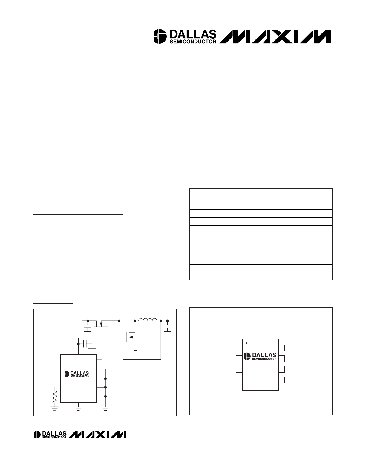
Typical Operating Circuit
Rev 1; 2/07
For pricing, delivery, and ordering information, please contact Maxim/Dallas Direct! at
1-888-629-4642, or visit Maxim’s website at www.maxim-ic.com.
Add “T” for Tape & Reel orders.
EconOscillator is a trademark of Dallas Semiconductor.
OUTPUT
PART
DS1090U-1+ 4MHz to 8MHz 1 8 μSOP
DS1090U-2+ 2MHz to 4MHz 2 8 μSOP
DS1090U-4+ 1MHz to 2MHz 4 8 μSOP
DS1090U-8+
DS1090U-16+
DS1090U-32+
FREQUENCY
RANGE
500kHz to
1MHz
250kHz to
500kHz
125kHz to
250kHz
PRE SCALER
8 8 μSOP
16 8 μSOP
32 8 μSOP
PINPACKAGE
V
IN
V
CC
DC-DC
STEP-DOWN
V
CC
DS1090
R
SET
45kΩ
TO 91kΩ
GND
CONVERTER
OUT
JC0
JC1
J0
J1
V
OUT
TOP VIEW
1
OUT
2
SET
V
3
CC
4
87JC1
DS1090
μSOP
JC0R
J1
6
J0GND
5
Page 2
DS1090
Low-Frequency, Spread-Spectrum
EconOscillator
2 _____________________________________________________________________
ABSOLUTE MAXIMUM RATINGS
RECOMMENDED DC OPERATING CONDITIONS
(TA= -40°C to +85°C)
DC ELECTRICAL CHARACTERISTICS
(VCC= +3.0V to +5.5V, TA= -40°C to +85°C, unless otherwise noted.)
Stresses beyond those listed under “Absolute Maximum Ratings” may cause permanent damage to the device. These are stress ratings only, and functional
operation of the device at these or any other conditions beyond those indicated in the operational sections of the specifications is not implied. Exposure to
absolute maximum rating conditions for extended periods may affect device reliability.
Voltage Range on VCCRelative to Ground ...........-0.5V to +6.0V
Voltage Range on Input Pins
Relative to Ground.................................-0.5V to (V
CC
+ 0.5V),
not to exceed 6.0V
Operating Temperature Range ...........................-40°C to +85°C
Storage Temperature Range .............................-55°C to +125°C
Soldering Temperature .......................................See IPC/JEDEC
J-STD-020A Specification
PARAMETER SYMBOL CONDITIONS MIN TYP MAX UNITS
Supply Voltage V
Input Logic 1 (J0, J1, JC0, JC1) V
Input Logic 0 (J0, J1, JC0, JC1) V
CC
(Note 1) 3.0 5.5 V
IH
IL
0.7 x
V
-0.3
CC
V
CC
0.3
+0.3 x
V
CC
+
V
V
Supply Current I
High-Level Output Voltage (OUT) V
Low-Level Output Voltage (OUT) V
High-Level Input Current
(J0, J1, JC0, JC1)
Low-Level Input Current
(J0, J1, JC0, JC1)
Resistor Current I
PARAMETER SYMBOL CONDITIONS MIN TYP MAX UNITS
CC
OH
OL
I
IH
I
RES
CL = 15pF, VCC = 3.3V, R
CL = 15pF, VCC = 5.5V, R
IOH = -4mA
VCC = min
IOL = 4mA 0.4 V
VIH = V
CC
VIL = 0V -1.0 µA
IL
VCC = max 150 µA
= 40kΩ 1.4
SET
= 40kΩ 1.7 3
SET
2.4 V
mA
+1.0 µA
Page 3
DS1090
Low-Frequency, Spread-Spectrum
EconOscillator
_____________________________________________________________________ 3
AC ELECTRICAL CHARACTERISTICS
(VCC= +3.0V to +5.5V, TA= -40°C to +85°C, unless otherwise noted.)
Note 1: All voltages referenced to ground.
Note 2: This is the change observed in output frequency due to changes in temperature or voltage.
Note 3: See the Typical Operating Characteristics section.
Note 4: Parameter is guaranteed by design and is not production tested.
Note 5: This is a percentage of the output period. Parameter is characterized but not production tested. This can be varied from
0% to 8%.
Note 6: This indicates the time between power-up and the outputs becoming active. An on-chip delay is intentionally introduced to
allow the oscillator to stabilize. t
STAB
is equivalent to ~500 clock cycles and is dependent upon the programmed
output frequency.
Note 7: Output voltage swings can be impaired at high frequencies combined with high output loading.
Internal Master Oscillator
Frequency
Output Frequency Tolerance f
Voltage Frequency Variation f
Temperature Frequency Variation f
Peak-to-Peak Dither (3)
(Note 5)
Power-Up Time
Load Capacitance CL (Note 7) 30 pF
Output Duty Cycle
Output Rise/Fall Time tR, tF CL = 15pF 20 ns
PARAMETER SYMBOL CONDITIONS MIN TYP MAX UNITS
f
MOSC
OUT
OUT
OUT
t
POR
t
STAB
4.0 8.0 MHz
VCC = 3.3V,
T
= +25°C
A
TA = +25°C, R
= 3.0V to 3.6V (Notes 2, 3)
V
CC
TA = +25°C, R
V
= 4.5V to 5.5V (Notes 2, 3)
CC
VCC = 3.3V
(Notes 2, 3, 4)
J0 = GND, J1 = GND 0
J0 = VCC, J1 = GND 2
J0 = GND, J1 = VCC 4
J0 = V
+
(Note 6) 0.1 0.5 ms
4MHz to 8MHz, TA = +25°C (Note 3) 45 55
<4MH z (Note 4) 50
, J1 = VCC 8
CC
SET
SET
= 60k,
= 60k,
-3.0 +3.0 %
-0.5 +0.5
%
-1.25 +1.25
-2.0 +2.0 %
%
%
Page 4

DS1090
Low-Frequency, Spread-Spectrum
EconOscillator
4 _____________________________________________________________________
Typical Operating Characteristics
(VCC= +3.3V, TA = +25°C, unless otherwise noted.)
SUPPLY CURRENT
vs. SUPPLY VOLTAGE
DS1090 toc01
SUPPLY VOLTAGE (V)
SUPPLY CURRENT (mA)
5.04.54.03.5
0.95
1.20
1.45
1.70
0.70
3.0 5.5
NO LOAD, TA = +25°C
40kΩ
60kΩ
80kΩ
SUPPLY CURRENT
vs. TEMPERATURE
DS1090 toc02
TEMPERATURE (°C)
SUPPLY CURRENT (mA)
603510-15
0.70
0.90
1.10
1.30
1.50
0.50
-40 85
NO LOAD, VCC = 3.3V
40kΩ
60kΩ
80kΩ
SUPPLY CURRENT
vs. OUTPUT LOADING
DS1090 toc03
LOAD CAPACITANCE (pF)
SUPPLY CURRENT (mA)
353025201510
1
2
3
4
0
540
TA = +25°C, R
SET
= 40kΩ
4V
3V
5V
OUTPUT VOLTAGE HIGH
vs. OUTPUT CURRENT
DS1090 toc04
OUTPUT CURRENT (mA)
OUTPUT VOLTAGE (V)
-1-2-3-4
2.8
2.9
3.0
3.1
2.7
-5 0
VCC = 3.0V
OUTPUT VOLTAGE LOW
vs. OUTPUT CURRENT
DS1090 toc05
OUTPUT CURRENT (mA)
OUTPUT VOLTAGE (V)
4321
0.1
0.2
0.3
0.4
0
05
VCC = 3.0V
OUTPUT FREQUENCY
vs. SUPPLY VOLTAGE
DS1090 toc06
SUPPLY VOLTAGE (V)
FREQUENCY (MHz)
5.04.54.03.5
5
6
7
8
9
10
4
3.0 5.5
TA = +25°C
60kΩ
80kΩ
40kΩ
Page 5

DS1090
Low-Frequency, Spread-Spectrum
EconOscillator
_____________________________________________________________________
5
Typical Operating Characteristics (continued)
(VCC= +3.3V, TA = +25°C, unless otherwise noted.)
OUTPUT FREQUENCY
10
9
8
7
FREQUENCY (MHz)
6
5
4
-40 85
5.0
2.5
0
FREQUENCY ERROR (%)
-2.5
-5.0
3.0 5.5
vs. TEMPERATURE
VCC = 3.3V
40kΩ
60kΩ
80kΩ
603510-15
TEMPERATURE (°C)
FREQUENCY ERROR
vs. SUPPLY VOLTAGE (FROM 3.3V)
TA = +25°C
80kΩ
40kΩ
SUPPLY VOLTAGE (V)
60kΩ
5.04.54.03.5
DS1090 toc07
DUTY CYCLE (%)
DS1090 toc10
FREQUENCY ERROR (%)
-1.0
-2.0
DUTY CYCLE
vs. TEMPERATURE
52
51
50
49
48
-40 85
VCC = 5V
DS1090U-1
TEMPERATURE (°C)
VCC = 3.3V
R
SET
= 40kΩ
603510-15
FREQUENCY ERROR
vs. TEMPERATURE (FROM +25°C)
2.0
VCC = 3.3V
1.0
0
-40 85
TEMPERATURE (°C)
60kΩ
40kΩ
603510-15
80kΩ
DS1090 toc08
DS1090 toc11
RESISTOR CURRENT
vs. RESISTOR VALUE
18
16
14
12
RESISTOR CURRENT (μA)
10
8
40 80
VCC = 3.3V, TA = +25°C
R
(kΩ)
SET
POWER SPECTRUM vs. SPREAD
0
OFF
-10
-20
±2%
-30
±4%
-40
±8%
POWER (dBm)
-50
-60
-70
-80
4.80 5.90
FREQUENCY (MHz)
5.35
VCC = 3.3V,
T
JC0 = JC1 = 1
706050
= +25°C,
A
DS1090 toc09
DS1090 toc12
Page 6

DS1090
Low-Frequency, Spread-Spectrum
EconOscillator
6 _____________________________________________________________________
Pin Description
Block Diagram
PIN NAME FUNCTION
1 OUT Oscillator Output
2R
3VCCPositive-Supply Terminal
4 GND Ground
5J0
6J1
7 JC0
8 JC1
Frequency Control Resistor Input
SET
Dither Amplitude (Percentage) Inputs
(see Table 2)
Dither Rate Divisor Inputs (see Table 1)
R
SET
V
GND
JC0
JC1
VOLTAGE-
BIAS CIRCUIT
DITHER
MASTER
OSCILLATOR
(VCO)
4MHz–8MHz
f
DITHER GENERATOR
MOD
f
MOSC
TRIANGLE
GENERATOR
(÷ 128)
+
∑
+
V
CC
CC
+
AMPLITUDE
(0, 2, 4, OR 8%)
J0
J1
DS1090
FACTORY
PROGRAMMED
PRESCALER
(÷ 1, 2, 4, 8, 16, OR 32)
DITHER RATE
(÷ 4, 8, 16, OR 32)
f
OSC
BUFFER
f
OUT
OUT
Page 7

DS1090
Low-Frequency, Spread-Spectrum
EconOscillator
_____________________________________________________________________ 7
Detailed Description
The DS1090 is a center-dithered, spread-spectrum silicon oscillator for use as an external clock in reducedEMI applications. With a combination of factoryprogrammed prescalers and a user-selected external
resistor, output frequencies from 125kHz to 8MHz can
be achieved. The output center frequency can be
dithered by selecting the desired dither rate and amplitude with discrete inputs J0, J1, JC0, and JC1.
The DS1090 contains four basic circuit blocks: master
oscillator, factory-programmed prescaler, dither generator, and the voltage-bias circuit that provides the feedback path to the master oscillator for frequency control
and dithering functions.
Master Oscillator
The master oscillator is programmable in the application by the use of an external resistor (R
SET
) tied to
ground (GND). Resistor values of 45kΩ to 91kΩ vary
the square-wave output frequency of the voltage-controlled master oscillator (f
MOSC
) from 8MHz down to
4MHz (see Figure 1).
The master oscillator (Hz) frequency can be stated as
Factory-Programmed Prescaler
The prescaler divides the frequency of the master oscillator by 1, 2, 4, 8, 16, or 32 to generate the squarewave output clock (f
OSC
). This divisor is factory-set and
is an ordering option.
Dither Generator
Spread-spectrum functionality is achieved by a userconfigurable divider (determines dither rate), a triangle
generator, and a user-configurable dither amplitude circuit (see
Block Diagram
).
The input to the triangle-wave generator is derived from
the internal master oscillator and is fed through a userconfigurable divider. The settings of control pins JC0
and JC1 determine this dither rate divisor setting (see
Table 1), dividing the master clock by 4, 8, 16, or 32.
The clock signal is further divided by 128 in the
triangle-wave generator, which results in a trianglewave signal of either 1/512th, 1/1024th, 1/2048th, or
1/4096th of the master oscillator (f
MOD
), depending
upon the user’s divisor setting.
The dithering frequency can be also expressed as the
result of
where Divisor is 4, 8, 16, or 32.
Figure 1. Master Oscillator Frequency
Figure 2. Center Frequency Dither Diagram
Table 1. Dither Rate Divisor Settings
MASTER OSCILLATOR FREQUENCY vs.
EXTERNAL RESISTOR SELECTION
9
8
7
(MHz)
6
MOSC
f
5
4
3
50
40
R
RESISTANCE (kΩ)
SET
80
7060
DS1090 fig01
90
E
+3 6461 11.
f
MOSC
≅
Re
sistor
(+ 1, 2, or 4% of f
Programmed f
(- 1, 2, or 4% of f
MOSC
MOSC
MOSC
)
)
MOSC
f
f
1
MOD
IF DITHER AMOUNT = 0%
DITHER
AMOUNT
(2, 4, OR 8%)
TIME
f
=
Divisor
MOSC
× 128
f
MOD
JC1 JC0
00 F
01 F
10 f
11 f
DITHERING PERCENTAGE
(f
MOSC
MOSC
MOSC
MOSC
MOSC
/n)
/ 512 4
/ 1024 8
/ 2048 16
/ 4096 32
DIVISOR
SETTING
Page 8

DS1090
Low-Frequency, Spread-Spectrum
EconOscillator
Maxim cannot assume responsibility for use of any circuitry other than circuitry entirely embodied in a Maxim product. No circuit patent licenses are
implied. Maxim reserves the right to change the circuitry and specifications without notice at any time.
8
_____________________Maxim Integrated Products, 120 San Gabriel Drive, Sunnyvale, CA 94086 408-737-7600
© 2007 Maxim Integrated Products is a registered trademark of Maxim Integrated Products.
is a registered trademark of Dallas Semiconductor Corporation.
Dither Percentage Settings
Dither amplitude (measured in percent ± from the master oscillator center frequency) is set using input pins
J0 and J1. This circuit uses a sense current from the
master oscillator bias circuit to adjust the amplitude of
the triangle-wave signal to a voltage level that modulates the master oscillator to a percentage of its resistor-set center frequency. This percentage is set in the
end application to be 0%, 2%, 4%, or 8% (see Table 2).
Application Information
Pin Connection
The DS1090 is intended to provide a fixed-frequency,
dithered clock to be used as a clock driver for DC-DC
converters and other applications requiring a lowfrequency EMI-reduced clock oscillator. All control pins
must be biased per Tables 1 and 2 for proper operation
for the individual application’s requirements. R
SET
must
be tied to ground (GND) by a customer-supplied resistor.
R
SET
Resistor Selection
The value of the resistor used to select the desired frequency is calculated using the formula in the
Master
Oscillator
section (see also Figure 1). It is recommended
to use, at minimum, a 1%-tolerance, 1/16th-watt component with a temperature coefficient that satisfies the overall stability requirements desired of the end-equipment.
Place the external R
SET
resistor as close as possible to
minimize lead inductance.
Power-Supply Decoupling
To achieve best results, it is highly recommended that a
decoupling capacitor is used on the IC power-supply
pins. Typical values of decoupling capacitors are 0.01µF
and 0.1µF. Use a high-quality, ceramic, surface-mount
capacitor, and mount it as close as possible to the V
CC
and GND pins of the IC to minimize lead inductance.
Table 2. Dither Percentage Setting
Package Information
For the latest package outline information, go to
www.maxim-ic.com/DallasPackInfo
.
Chip Information
TRANSISTOR COUNT: 1883
SUBSTRATE CONNECTED TO GROUND
J1 J0 DITHER PERCENT (%)
00 0
01 2
10 4
11 8
 Loading...