

Page 1
General Description
The DS1088L is a low-cost clock generator that produces a square-wave output without external timing
components. The fixed-frequency oscillator is available
in factory-calibrated frequencies from 312kHz to
133MHz. The DS1088L has a power-down pin for
power-sensitive applications.
Applications
Printers
Copiers
Automotive Telematics
Computer Peripherals
POS Terminals
Cable Modems
Features
♦ Factory-Programmed, Square-Wave Generator
from 312kHz to 133MHz
♦ Single Output
♦ No External Timing Components Required
♦ 2.7V to 3.6V Supply
♦ Power-Down Mode
♦ 1.0% Frequency Tolerance Over Temperature
and Voltage
♦ Wide Temperature Range (-20°C to +85°C)
DS1088L
Low-Cost Fixed-Frequency EconOscillator™
______________________________________________ Maxim Integrated Products 1
PDN
GNDGND
1
2
87DNC
DNCV
CC
V
CC
OUT
TOP VIEW
3
4
6
5
DS1088L
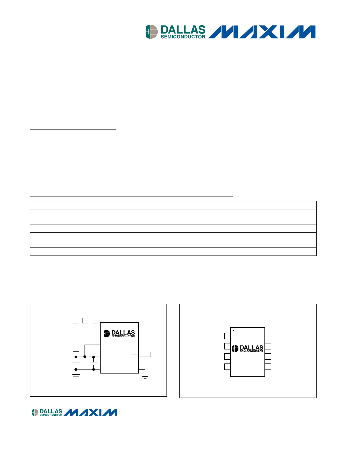
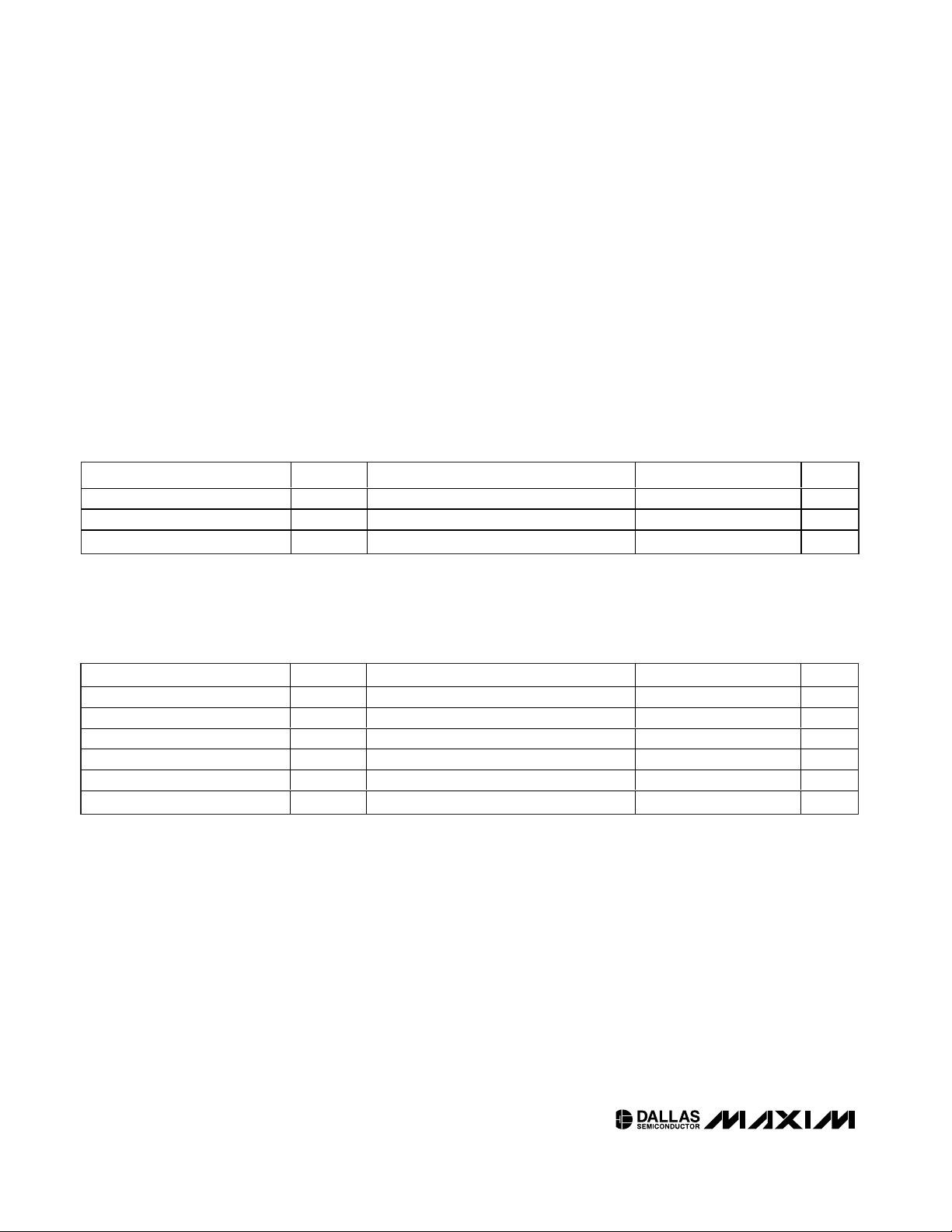
Pin Configuration
V
CC
OUT
PDN
DNC
GND
V
CC
V
CC
V
CC
DECOUPLING CAPACITORS
(0.1µF AND 0.01µF)
DNC
GND
312kHz TO 133MHz
OUTPUT
DS1088L
Typical Operating Circuit
Ordering Information
Rev 1; 5/05
For pricing, delivery, and ordering information, please contact Maxim/Dallas Direct! at
1-888-629-4642, or visit Maxim’s website at www.maxim-ic.com.
EconOscillator is a trademark of Dallas Semiconductor.
PART
FREQUENCY (MHz) TEMP RANGE
PIN-PACKAGE
DS1088LU-02
2.048 -20°C to +85°C
8 µSOP
DS1088LU-10
10.0 -20°C to +85°C
8 µSOP
DS1088LU-16
16.6 -20°C to +85°C
8 µSOP
DS1088LU-66
66.6 -20°C to +85°C
8 µSOP
DS1088LU-100
100.0 -20°C to +85°C
8 µSOP
DS1088LU-yyy
* -20°C to +85°C
8 µSOP
yyy = frequency
*Email Custom_EconOscillators_Info@dalsemi.com for information/questions concerning custom frequencies.
Page 2
DS1088L
Low-Cost Fixed-Frequency EconOscillator™
2 _____________________________________________________________________
ABSOLUTE MAXIMUM RATINGS
RECOMMENDED OPERATING CONDITIONS
(TA= -20°C to +85°C)
Stresses beyond those listed under “Absolute Maximum Ratings” may cause permanent damage to the device. These are stress ratings only, and functional
operation of the device at these or any other conditions beyond those indicated in the operational sections of the specifications is not implied. Exposure to
absolute maximum rating conditions for extended periods may affect device reliability.
PARAMETER
CONDITIONS
UNITS
Supply Voltage V
CC
(Note 1) 2.7 3.6 V
High-Level Input Voltage (PDN)V
IH
V
Low-Level Input Voltage (PDN)V
IL
V
DC ELECTRICAL CHARACTERISTICS
(VCC= 2.7V to 3.6V, TA= -20°C to +85°C.)
PARAMETER
CONDITIONS
UNITS
High-Level Output Voltage (OUT)
V
OH
IOH = -4mA, VCC = min
V
Low-Level Output Voltage (OUT)
V
OL
IOL = 4mA 0.4 V
High-Level Input Current (PDN)IIHVCC = 3.6V 1 µA
Low-Level Input Current (PDN)IILVIL = 0 -1 µA
Supply Current (Active) I
CC
VCC = 3.6V, CL = 15pF, f0 = 133MHz 15 24 mA
Standby Current (Power-Down) I
CCQ
Power-down mode 10 µA
Voltage Range on VCCRelative to Ground ..........-0.5V to +6.0V
Voltage Range on PDN Relative
to Ground*..............................................-0.5V to (V
CC
+ 0.5V)
Operating Temperature Range ...........................-20°C to +85°C
Storage Temperature Range ............................-55°C to +125°C
Soldering Temperature ....................See IPC/JEDEC J-STD-020
*Not to exceed +6.0V.
SYMBOL
MIN TYP MAX
SYMBOL
0.7 x V
CC
-0.3 0.3 x V
MIN TYP MAX
VCC - 0.4
V
CC
+ 0.3
CC
Page 3

DS1088L
Low-Cost Fixed-Frequency EconOscillator™
_____________________________________________________________________ 3
OSCILLATOR CHARACTERISTICS
(VCC= 2.7V to 3.6V, TA= -20°C to +85°C.)
PARAMETER
CONDITIONS
UNITS
Output Frequency Range
Available
f
0
MHz
Output Frequency Tolerance
∆f
0
f
0
VCC = 3.3V, TA = +25°C (Note 8)
%
Voltage Frequency Variation
∆f
V
f
0
Over voltage range, TA = +25°C (Note 2)
%
-20°C to +25°C
Temperature Frequency Variation
∆f
T
f
0
Over temperature range,
%
Frequency Variation Over Voltage
and Temperature
∆f
V,T
f
0
Over voltage and temperature range
%
AC ELECTRICAL CHARACTERISTICS
(VCC= 2.7V to 3.6V, TA= -20°C to +85°C.)
PARAMETER
CONDITIONS
UNITS
Power-Up Time
t
POR
+
t
STAB
(Note 5) 100 µs
OUT Disabled After Entering
Power-Down Mode
t
PDN
(Note 6) 7 µs
Load Capacitance C
L
(Note 7) 15 50 pF
f0 < 80MHz, f0 ≥ 80MHz 40 60
Output Duty Cycle (OUT)
f
0
< 80MHz 50
%
Note 1: All voltages are referenced to ground.
Note 2: This is the change in output frequency due to changes in voltage at T
A
= +25°C.
Note 3: This is the change in output frequency due to changes in temperature from the +25°C frequency at V
CC
= 3.3V.
Note 4: Guaranteed by design.
Note 5: This indicates the time elapsed between power-up and the output becoming active. An on-chip delay is intentionally intro-
duced to allow the oscillator to stabilize. t
STAB
is equivalent to approximately 512 clock cycles and will depend on the pro-
grammed oscillator frequency.
Note 6: Output disabled in 2 cycles or less of the output frequency.
Note 7: Output voltage swings may be impaired at high frequencies combined with high-output loading.
Note 8: Typical frequency shift due to aging is within ±0.2%. Aging stressing includes level 1 moisture reflow preconditioning (24hr
+125°C bake, 168hr +85°C/85%RH moisture soak, and three solder reflow passes +240°C +0°C/-5°C peak) followed by
1000hr (max) V
CC
biased +125°C OP/L, 1000hr unbiased +150°C bake, 1000 temperature cycles at -55°C to +125°C and
168hr +121°C/2 ATM steam/unbiased autoclave.
SYMBOL
VCC = 3.3V (Notes 3, 4)
SYMBOL
MIN TYP MAX
0.3124 133.3
-0.3 +0.3
-0.35 +0.35
-0.7 +0.7
+25°C to +85°C -0.5 +0.5
-1.0 +1.0
MIN TYP MAX
Page 4

DS1088L
Low-Cost Fixed-Frequency EconOscillator™
4 _____________________________________________________________________
ACTIVE SUPPLY CURRENT
vs. TEMPERATURE
DS1088L toc01
TEMPERATURE (°C)
SUPPLY CURRENT (mA)
55305
4
5
6
7
8
9
10
3
-20 80
VCC = 3.3V
C
L
= 1.8pF
133MHz
100MHz
80MHz
ACTIVE SUPPLY CURRENT
vs. SUPPLY VOLTAGE
DS1088L toc02
SUPPLY VOLTAGE (V)
SUPPLY CURRENT (mA)
3.33.12.9
4
5
6
7
8
9
10
3
2.7 3.5
TA = +25°C
C
L
= 1.8pF
133MHz
100MHz
80MHz
ACTIVE SUPPLY CURRENT
vs. SUPPLY VOLTAGE
DS1088L toc03
SUPPLY VOLTAGE (V)
SUPPLY CURRENT (mA)
2.9 3.1
3.3
3.5
7
8
9
10
11
12
13
14
15
6
2.7
TA = +25°C
C
L
= 15pF
133MHz
100MHz
80MHz
SHUTDOWN SUPPLY CURRENT
vs. TEMPERATURE
DS1088L toc04
TEMPERATURE (°C)
SHUTDOWN CURRENT (µA)
80
55
305
1.6
1.7
1.8
1.9
2.0
2.1
2.2
2.3
2.4
2.5
1.5
-20
PDN = 0V
VCC = 3.3V
FREQUENCY ERROR
vs. SUPPLY VOLTAGE
DS1088L toc05
SUPPLY VOLTAGE (V)
FREQUENCY ERROR (%)
2.9 3.1 3.3 3.5
-0.15
-0.10
-0.05
0
0.05
0.10
0.15
0.20
-0.20
2.7
TA = +25°C
C
L
RL = 1.8pF 500Ω
133MHz
100MHz
80MHz
FREQUENCY ERROR
vs. TEMPERATURE
DS1088L toc06
TEMPERATURE (°C)
FREQUENCY ERROR (%)
80
55
30
5
-0.3
-0.2
-0.1
0
0.1
0.2
0.3
-0.4
-20
VCC = 3.3V
100MHz
133MHz
100MHz
80MHz
80MHz
TA = +25°C
C
L
RL = 1.8pF 500Ω
DUTY CYCLE
vs. SUPPLY VOLTAGE
DS1088L toc07
SUPPLY VOLTAGE (V)
DUTY CYCLE (%)
3.1
2.9
3.3
50
51
52
53
54
55
56
49
2.7
3.5
133MHz
100MHz
80MHz
TA = +25°C
C
L
RL = 1.8pF 500Ω
DUTY CYCLE
vs. TEMPERATURE
DS1088L toc08
TEMPERATURE (°C)
DUTY CYCLE (%)
8055
5
30
49
50
51
52
54
53
55
56
48
-20
133MHz
100MHz
80MHz
VCC = 3.3V
TA = +25°C
C
L
RL = 1.8pF 500Ω
Typical Operating Characteristics
(VCC= 3.3V, TA= +25°C, unless otherwise noted.)
Page 5

DS1088L
Low-Cost Fixed-Frequency EconOscillator™
Maxim cannot assume responsibility for use of any circuitry other than circuitry entirely embodied in a Maxim product. No circuit patent licenses are
implied. Maxim reserves the right to change the circuitry and specifications without notice at any time.
Maxim Integrated Products, 120 San Gabriel Drive, Sunnyvale, CA 94086 408-737-7600 _____________________ 5
© 2005 Maxim Integrated Products Printed USA is a registered trademark of Maxim Integrated Products, Inc.
is a registered trademark of Dallas Semiconductor Corporation.
Detailed Description
The DS1088L is a low-cost clock generator that produces a square-wave output without external timing
components. The fixed-frequency oscillator is available
in factory-calibrated frequencies from 312kHz to
133MHz. The DS1088L has a power-down pin for
power-sensitive applications. A block diagram of the
DS1088L is shown in Figure 1.
Output Frequency
The internal oscillator frequency is divided by the factory-programmed prescaler to produce an output frequency of 312kHz to 133MHz. See the Standard
Frequency Options table for a list of standard frequencies. Contact factory for custom frequencies.
Power-Down Mode
The PDN pin disables the internal oscillator and the
oscillator output for power-sensitive applications. The
power-down pin must remain low for at least two output
frequency cycles plus 10µs for deglitching purposes.
On power-up, the output is disabled until power is stable and the voltage-controlled oscillator has generated
512 clock cycles.
Applications Information
Power-Supply Decoupling
To achieve the best results when using the DS1088L,
the power supply must be decoupled with 0.01µF and
0.1µF high-quality, ceramic, surface-mount capacitors.
Surface-mount components minimize lead inductance,
which improves performance, and tend to have adequate high-frequency response for decoupling applications. These capacitors should be placed as close to
the VCCand GND pins as possible.
Chip Topology
TRANSISTOR COUNT: 4507
SUBSTRATE CONNECTED TO GROUND.
Package Information
For the latest package outline information, go to
www.maxim-ic.com/DallasPackInfo
.
Pin Description
PIN
FUNCTION
1 OUT Oscillator Output
2VCCPower Supply
3VCCPower Supply
4 GND Ground
5 GND Ground
6 PDN
Power-Down. When the pin is high, the
oscillator is enabled. When the pin is
low, the oscillator is disabled
(power-down mode).
7 DNC
Do Not Connect. The DNC pins are
internally connected to ground.
8 DNC Do Not Connect
Figure 1. Block Diagram
V
CC
PDN
OUT
(312kHz
TO 133MHz)
EEPROM
CONTROL
VOLTAGE-
CONTROLLED
OSCILLATOR
80MHz TO 160MHz
PRESCALER
BY 1, 2, 4...256
GND
V
CC
DS1088L
NAME
 Loading...