

Page 1
General Description
The DS1086 EconOscillator™ is a programmable clock
generator that produces a spread-spectrum (dithered)
square-wave output of frequencies from 260kHz to
133MHz. The selectable dithered output reduces radiated-emission peaks by dithering the frequency 2% or
4% below the programmed frequency. The DS1086 has
a power-down mode and an output-enable control for
power-sensitive applications. All the device settings are
stored in nonvolatile (NV) EEPROM memory allowing it
to operate in stand-alone applications.
Applications
Printers
Copiers
PCs
Computer Peripherals
Cell Phones
Cable Modems
Features
o User-Programmable Square-Wave Generator
o Frequencies Programmable from 260kHz to
133MHz
o 2% or 4% Selectable Dithered Output
o Glitchless Output-Enable Control
o 2-Wire Serial Interface
o Nonvolatile Settings
o 5V Supply
o No External Timing Components Required
o Power-Down Mode
o 10kHz Master Frequency Step Size
o EMI Reduction
DS1086
Spread-Spectrum EconOscillator
________________________________________________________________
Maxim Integrated Products
1
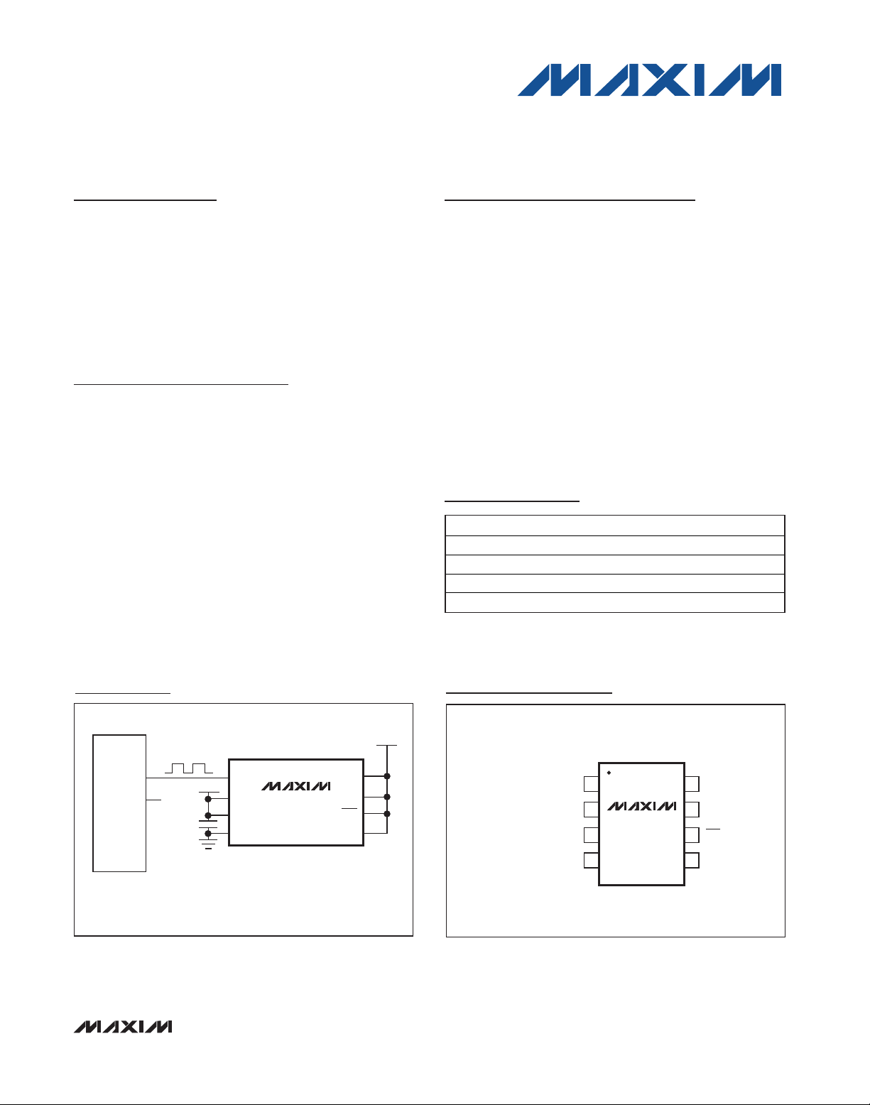
Pin Configuration
Ordering Information
Typical Operating Circuit
19-6224; Rev 2; 3/12
For pricing, delivery, and ordering information, please contact Maxim Direct at 1-888-629-4642,
or visit Maxim’s website at www.maxim-ic.com.
Note: Contact the factory for custom settings.
+
Denotes a lead(Pb)-free/RoHS-compliant package.
PART TEMP RANGE PIN-PACKAGE
DS1086U 0°C to +70°C 8 µSOP
DS1086U+ 0°C to +70°C 8 µSOP
DS1086Z 0°C to +70°C 8 SO
DS1086Z+ 0°C to +70°C 8 SO
EconOscillator is a trademark of Maxim Integrated Products, Inc.
MICRO-
PROCESSOR
XTL1/OSC1
XTL2/OSC2
*SDA AND SCL CAN BE CONNECTED DIRECTLY HIGH IF THE DS1086 NEVER NEEDS
TO BE PROGRAMMED IN-CIRCUIT, INCLUDING DURING PRODUCTION TESTING.
DITHERED 260kHz TO
133MHz OUTPUT
OUT
V
CC
N.C.
DECOUPLING CAPACITORS
(0.1µF and 0.01µF)
SPRD
V
CC
GND
DS1086
SCL*
SDA*
PDN
V
CC
OE
TOP VIEW
OUT
V
1
2
DS1086
3
CC
4
µSOP/SO
87SCL
SDASPRD
PDN
6
OEGND
5
Page 2
DS1086
Spread-Spectrum EconOscillator
2 _______________________________________________________________________________________
ABSOLUTE MAXIMUM RATINGS
RECOMMENDED DC OPERATING CONDITIONS
(VCC= 5V ±5%, TA= 0°C to +70°C.)
Stresses beyond those listed under “Absolute Maximum Ratings” may cause permanent damage to the device. These are stress ratings only, and functional
operation of the device at these or any other conditions beyond those indicated in the operational sections of the specifications is not implied. Exposure to
absolute maximum rating conditions for extended periods may affect device reliability.
DC ELECTRICAL CHARACTERISTICS
(VCC= 5V ±5%, TA= 0°C to +70°C.)
Voltage on VCCRelative to Ground ......................-0.5V to +6.0V
Voltage on SPRD, PDN, OE, SDA,
SCL Relative to Ground (See Note 1).......-0.5 to (V
CC
+ 0.5V)
Continuous Power Dissipation (T
A
= +70°C)
µSOP (derate 4.5mW/°C above +70°C)........................362mW
SO (derate 5.9mW/°C above +70°C).........................470.6mW
Junction Temperature......................................................+150°C
Operating Temperature Range...............................0°C to +70°C
Storage Temperature Range .............................-55°C to +125°C
Soldering Temperature (reflow)
Lead(Pb)-free................................................................+260°C
Containing lead(Pb) .....................................................+240°C
Note 1: This voltage must not exceed 6.0V.
PARAMETER SYMBOL CONDITIONS MIN TYP MAX UNITS
Supply Voltage V
High-Level Input Voltage
(SDA, SCL)
Low-Level Input Voltage
(SDA, SCL)
High-Level Input Voltage
(SPRD, PDN, OE)
Low-Level Input Voltage
(SPRD, PDN, OE)
CC
V
V
V
V
(Note 1) 4.75 5.00 5.25 V
IH
IL
IH
IL
0.7 x
V
CC
-0.3
2
-0.3 0.8 V
VCC +
0.3
0.3 x
V
CC
V
CC
0.3
+
V
V
V
PARAMETER SYMBOL CONDITIONS MIN TYP MAX UNITS
High-Level Output Voltage (OUT) V
Low-Level Output Voltage (OUT) V
High-Level Input Current I
Low-Level Input Current I
Supply Current (Active)
Standby Current (Power-Down) I
OH
OL
IH
IL
I
CC
CCQ
IOH = -4mA, VCC = min 2.4 V
IOL = 4mA 0.4 V
VCC = 5.25V 1 µA
VIL = 0V -1 µA
CL = 15pF (output at default frequency) 35 mA
Power-down mode 35 µA
Page 3
DS1086
Spread-Spectrum EconOscillator
_______________________________________________________________________________________ 3
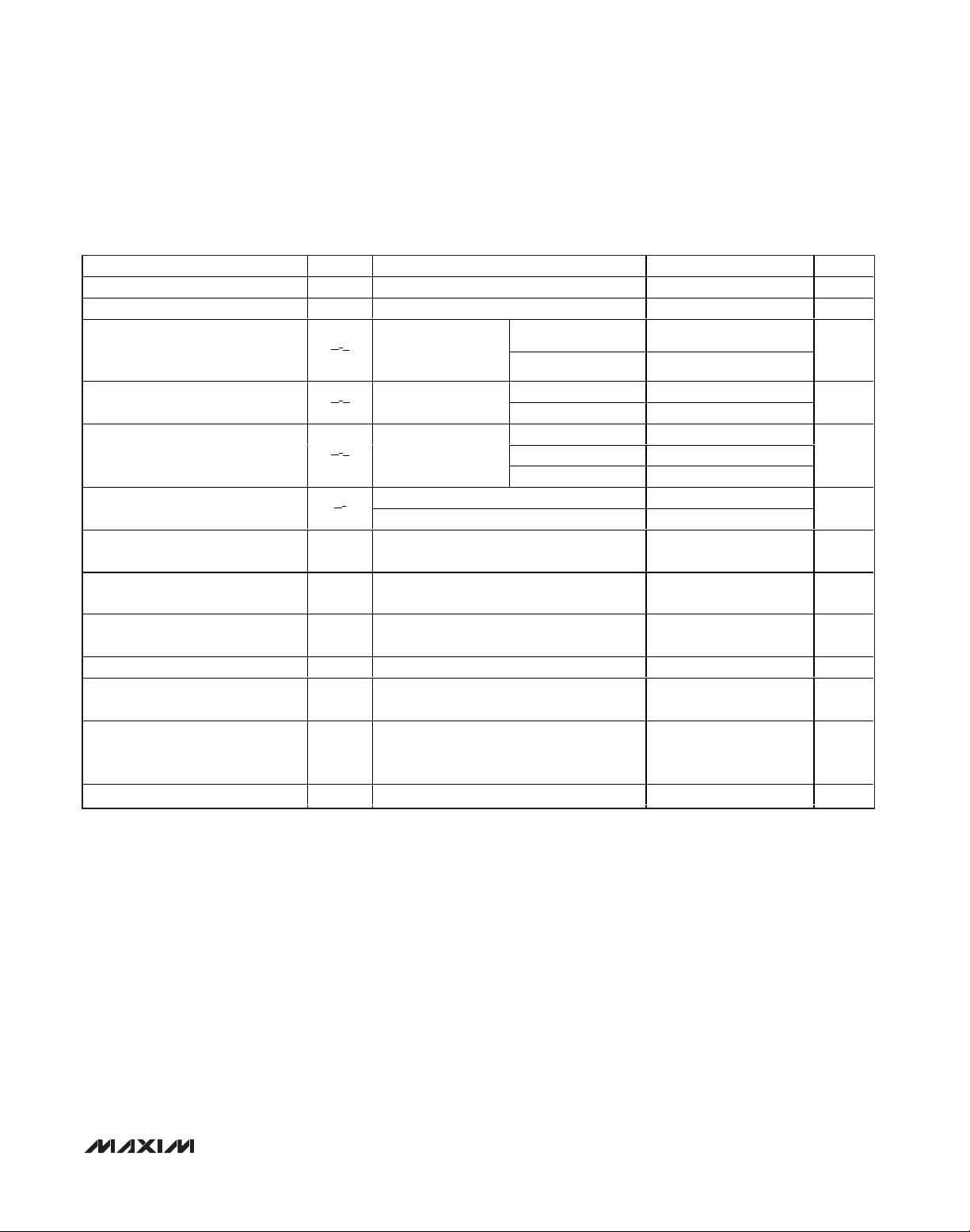
MASTER OSCILLATOR CHARACTERISTICS
(VCC= 5V ±5%, TA= 0°C to +70°C.)
PARAMETER SYMBOL CONDITION MIN TYP MAX UNITS
Master Oscillator Range f
Default Master Oscillator Frequency f
Master Oscillator Frequency
Tolerance
Voltage Frequency Variation
Dither Frequency Range
Integral Nonlinearity of Frequency
DAC
DAC Step Size
DAC Span
DAC Default Factory default register setting 500 decimal
Offset Step Size
Offset Default OS
Dither Rate f0/4096 Hz
OSC
INL Entire range (Note 7) -0.4 +0.4 %
(Note 2) 66 133 MHz
0
VCC = 5V,
∆ f
0
T
= +25°C
f
∆
f
∆
f
∆
f
A
0
(Notes 3,17)
f
Over voltage range,
V
0
f
T
0
f
0 Prescaler bit J0 = 0 (Note 6) 4
= +25°C (Note 4)
T
A
Over temperature
range, V
(Note 5)
Prescaler bit J0 = 1 (Note 6) 2
∆ between two consecutive DAC values
(Note 8)
Frequency range for one offset setting
(see Table 2)
∆ between two consecutive offset values
(see Table 2)
Factory default OFFSET register setting
(5 LSBs) (see Table 2)
CC
= 5V
Default frequency (f0) -0.75 +0.75
DAC step size -0.75 +0.75
Default frequency -0.75 +0.75
DAC step size -0.75 +0.75
Default frequency -0.5 +0.5
133MHz -0.5 +0.5Temperature Frequency Variation
66MHz -1.0 +1.0
97.1 MHz
10 kHz
10.24 MHz
5.12 MHz
RANGE
(5 LSBs of
RANGE register)
%
%
%
%
hex
Page 4
DS1086
Spread-Spectrum EconOscillator
4 _______________________________________________________________________________________
AC ELECTRICAL CHARACTERISTICS
(VCC= 5V ±5%, TA= 0°C to +70°C.)
p
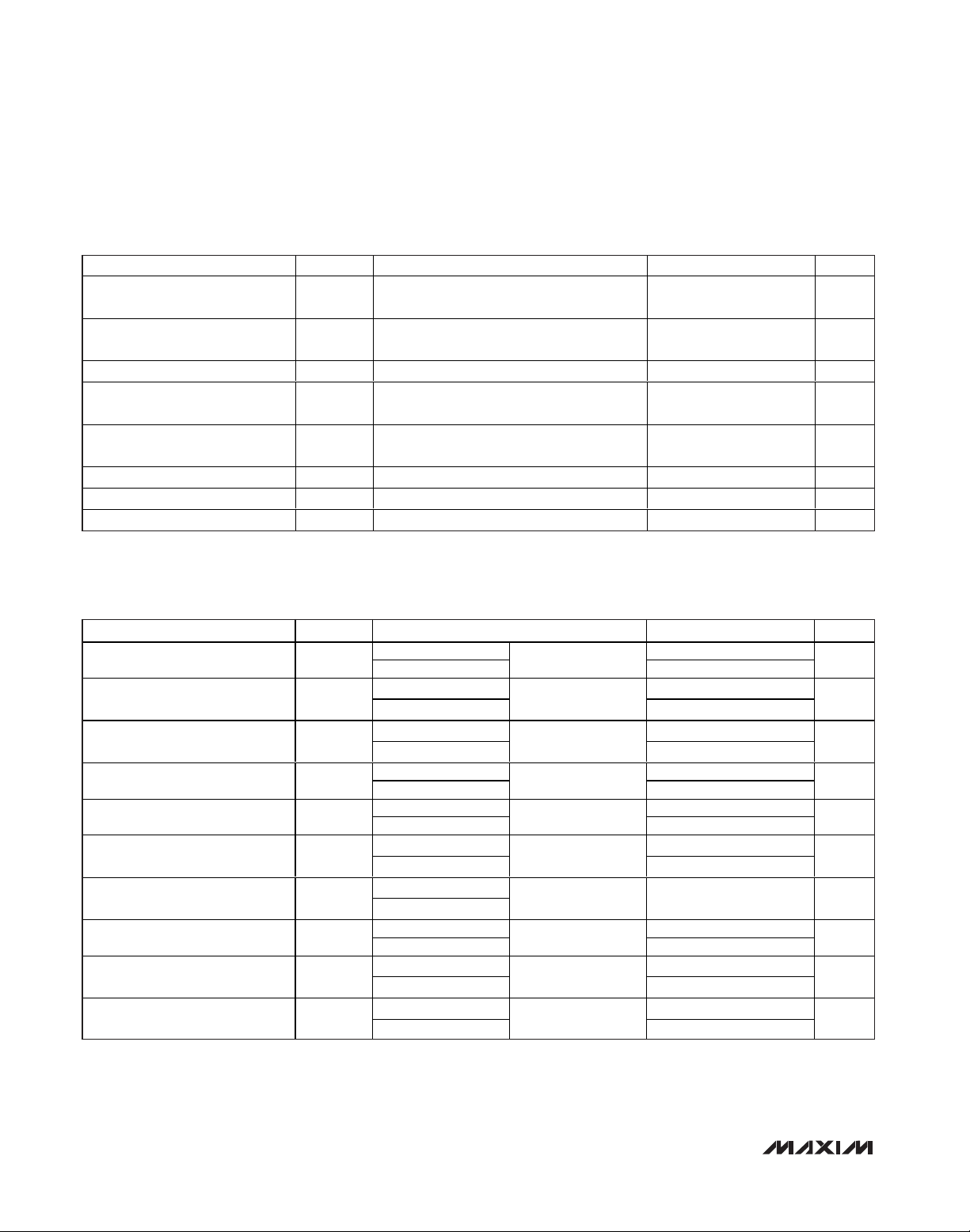
AC ELECTRICAL CHARACTERISTICS: 2-WIRE INTERFACE
(VCC= 5V ±5%, TA= 0°C to +70°C.)
PARAMETER SYMBOL CONDITION MIN TYP MAX UNITS
Frequency Stable After Prescaler
Change
Frequency Stable After DAC or
Offset Change
Power-Up Time t
Enable of OUT After Exiting
Power-Down Mode
OUT High-Z After Entering
Power-Down Mode
Load Capacitance C
Output Duty Cycle (OUT) 40 60 %
PDN Rise/Fall Time 1µs
+ t
or
t
stab
t
pdn
(Note 9) 0.2 1 ms
(Note 10) 0.1 0.5 ms
stab
(Note 11) 15 50 pF
L
1 Period
500 µs
0.1 ms
PARAMETER SYMBOL CONDITION MIN TYP MAX UNITS
SCL Clock Frequency f
Bus Free Time Between a STOP
and START Condition
Hold Time (Repeated) START
Condition
LOW Period of SCL t
HIGH Period of SCL t
Setup Time for a Repeated
START
Data Hold Time t
Data Setup Time t
Rise Time of Both SDA and SCL
Signals
Fall Time of Both SDA and SCL
Signals
SCL
t
BUF
t
HD:STA
LOW
HIGH
t
SU:STA
HD:DAT
SU:DAT
t
R
t
F
Fast mode 400
Standard mode
Fast mode 1.3
Standard mode
Fast mode 0.6
Standard mode
Fast mode 1.3
Standard mode
Fast mode 0.6
Standard mode
Fast mode 0.6
Standard mode
Fast mode
Standard mode
Fast mode 100
Standard mode
Fast mode 20 + 0.1C
Standard mode
Fast mode 20 + 0.1C
Standard mode
(Note 12)
(Note 12)
(Notes 12, 13)
(Note 12)
(Note 12)
(Note 12)
(Notes 12, 14, 15) 0 0.9 µs
(Note 12)
(Note 16)
(Note 16)
4.7
4.0
4.7
4.0
4.7
250
20 + 0.1C
20 + 0.1C
B
B
B
B
100
300
1000
300
1000
kHz
µs
µs
µs
µs
µs
ns
ns
ns
Page 5
DS1086
Spread-Spectrum EconOscillator
_______________________________________________________________________________________ 5
AC ELECTRICAL CHARACTERISTICS: 2-WIRE INTERFACE (continued)
(VCC= 5V ±5%, TA= 0°C to +70°C.)
Note 1: All voltages are referenced to ground.
Note 2: DAC and OFFSET register settings must be configured to maintain the master oscillator frequency within this range.
Correct operation of the device is not guaranteed if these limits are exceeded.
Note 3: This is the absolute accuracy of the master oscillator frequency at the default settings.
Note 4: This is the change that is observed in master oscillator frequency with changes in voltage from nominal voltage at
T
A
= +25°C.
Note 5: This is the percentage frequency change from the +25°C frequency due to temperature at V
CC
= 5V. The maximum temperature change varies with the master oscillator frequency setting. The minimum occurs at the default master oscillator
frequency (f
default
). The maximum occurs at the extremes of the master oscillator frequency range (66MHz or 133MHz)
(see Figure 2).
Note 6: The dither deviation of the master oscillator frequency is unidirectional and lower than the undithered frequency.
Note 7: The integral nonlinearity of the frequency adjust DAC is a measure of the deviation from a straight line drawn between the
two endpoints of a range. The error is in percentage of the span.
Note 8: This is true when the prescaler = 1.
Note 9: Frequency settles faster for small changes in value. During a change, the frequency transitions smoothly from the original
value to the new value.
Note 10: This indicates the time elapsed between power-up and the output becoming active. An on-chip delay is intentionally
introduced to allow the oscillator to stabilize. t
stab
is equivalent to approximately 512 master clock cycles and therefore
depends on the programmed clock frequency.
Note 11: Output voltage swings can be impaired at high frequencies combined with high output loading.
Note 12: A fast-mode device can be used in a standard-mode system, but the requirement t
SU:DAT
> 250ns must then be met.
This is automatically the case if the device does not stretch the LOW period of the SCL signal. If such a device does
stretch the LOW period of the SCL signal, it must output the next data bit to the SDA line at least t
R MAX
+ t
SU:DAT
=
1000ns + 250ns = 1250ns before the SCL line is released.
Note 13: After this period, the first clock pulse is generated.
Note 14: A device must internally provide a hold time of at least 300ns for the SDA signal (referred to as the V
IH MIN
of the SCL sig-
nal) in order to bridge the undefined region of the falling edge of SCL.
Note 15: The maximum t
HD:DAT
need only be met if the device does not stretch the LOW period (t
LOW
) of the SCL signal.
Note 16: C
B
—total capacitance of one bus line, timing referenced to 0.9 x VCCand 0.1 x VCC.
Note 17: Typical frequency shift due to aging is ±0.5%. Aging stressing includes Level 1 moisture reflow preconditioning (24hr
+125°C bake, 168hr 85°C/85%RH moisture soak, and 3 solder reflow passes +240 +0/-5°C peak) followed by 1000hr
max V
CC
biased 125°C HTOL, 1000 temperature cycles at -55°C to +125°C, 96hr 130°C/85%RH/5.5V HAST and 168hr
121°C/2 ATM Steam/Unbiased Autoclave.
PARAMETER SYMBOL CONDITION MIN TYP MAX UNITS
Setup Time for STOP t
Capacitive Load for Each Bus
Line
NV Write-Cycle Time t
Input Capacitance C
SU:STO
C
WR
Fast mode 0.6
Standard mode 4.0
(Note 16) 400 pF
B
I
5pF
10 ms
µs
Page 6

Typical Operating Characteristics
(VCC= 5.0V, TA= 25°C, unless otherwise noted)
DS1086
Spread-Spectrum EconOscillator
6 _______________________________________________________________________________________
SUPPLY CURRENT vs. TEMPERATURE
DS1086 toc01
TEMPERATURE (°C)
CURRENT (mA)
605030 402010
11
12
13
14
15
16
17
18
19
20
10
070
SUPPLY CURRENT vs. VOLTAGE
DS1086 toc02
VOLTAGE (V)
CURRENT (mA)
5.155.054.954.854.75 5.25
11
12
13
14
15
16
17
18
19
20
10
SUPPLY CURRENT vs. PRESCALER
DS1086 toc03
PRESCALER
CURRENT (mA)
200150100500250
11
12
13
14
15
16
17
18
19
20
10
5.25V
5.0V
4.75V
SUPPLY CURRENT vs. PRESCALER
DS1086 toc04
PRESCALER
CURRENT (mA)
200150100500250
11
12
13
14
15
16
17
18
19
20
10
70°C, 25°C, AND 0°C
SUPPLY CURRENT vs. TEMPERATURE
WITH OE = 0
DS1086 toc05
TEMPERATURE (°C)
CURRENT (mA)
605030 402010
1
2
3
4
5
6
7
8
9
10
0
070
SUPPLY CURRENT vs. TEMPERATURE
WITH PDN = 0
DS1086 toc06
TEMPERATURE (°C)
CURRENT (µA)
605030 402010
1
2
3
4
5
6
7
8
9
10
0
070
FREQUENCY PERCENT CHANGE
vs. SUPPLY VOLTAGE
DS1086 toc07
VOLTAGE (V)
FREQUENCY PERCENT CHANGE FROM 5V
5.155.054.954.85
-0.8
-0.6
-0.4
-0.2
0
0.2
0.4
0.6
0.8
1.0
-1.0
4.75 5.25
FREQUENCY PERCENT CHANGE
vs. TEMPERATURE
DS1086 toc08
TEMPERATURE (°C)
FREQUENCY PERCENT CHANGE FROM 25°C
605030 402010
-0.8
-0.6
-0.4
-0.2
0
0.2
0.4
0.6
0.8
1.0
-1.0
070
Page 7

DS1086
Spread-Spectrum EconOscillator
_______________________________________________________________________________________ 7
Pin Description
Processor-Controlled Mode
Stand-Alone Mode
Figure 1. Clock Spectrum Dither Comparison
Figure 2. Temperature Variation Over Frequency
PIN NAME FUNCTION
1 OUT Oscillator Output
2 SPRD Dither Enable. When the pin is high, the dither is enabled. When the pin is low, the dither is disabled.
3VCCPower Supply
4 GND Ground
5OE
6 PDN
7 SDA
8 SCL
CLOCK SPECTRUM COMPARISON
(9kHz BW, PEAK DETECT)
0
CRYSTAL OSC
-5
-10
-15
DS1086 4% DITHER
-20
-25
-30
RELATIVE AMPLITUDE (dBm)
-35
-40
90 95
Output Enable. When the pin is high, the output buffer is enabled. When the pin is low, the output is
disabled but the master oscillator is still on.
Power-Down. When the pin is high, the master oscillator is enabled. When the pin is low, the master
oscillator is disabled (power-down mode).
2-Wire Serial Data. This pin is for serial data transfer to and from the device. The pin is open drain
and can be wire-OR’ed with other open-drain or open-collector interfaces.
2-Wire Serial Clock. This pin is used to clock data into the device on rising edges and clock data out
on falling edges.
MAXIMUM TEMPERATURE VARIATION
vs. MASTER FREQUENCY
2.0
DS1086 NO DITHER
FREQUENCY (MHz)
DS1086 fig01
9491 9392
1.5
1.0
0.5
0
-0.5
-1.0
FREQUENCY % CHANGE FROM 25°C
-1.5
-2.0
66.00 133.00
82.75 116.2599.50
FREQUENCY (MHz)
DS1086 fig02
V
DITHERED 260kHz TO
133MHz OUTPUT
V
CC
DECOUPLING CAPACITORS
(0.1µF and 0.01µF)
OUT
SPRD
V
GND
DS1086
CC
4.7kΩ 4.7kΩ
SCL
SDA
V
PDN
OE
CC
MICRO-
PROCESSOR
XTL1/OSC1
2-WIRE
CC
INTERFACE
XTL2/OSC2
*SDA AND SCL CAN BE CONNECTED DIRECTLY HIGH IF THE DS1086 NEVER NEEDS
TO BE PROGRAMMED IN-CIRCUIT, INCLUDING DURING PRODUCTION TESTING.
DITHERED 260kHz TO
133MHz OUTPUT
OUT
V
CC
N.C.
DECOUPLING CAPACITORS
(0.1µF and 0.01µF)
SPRD
V
GND
DS1086
CC
SCL*
SDA*
PDN
V
CC
OE
Page 8

DS1086
Spread-Spectrum EconOscillator
8 _______________________________________________________________________________________
Detailed Description
A block diagram of the DS1086 is shown in Figure 3.
The internal master oscillator generates a square wave
with a 66MHz to 133MHz frequency range. The frequency of the master oscillator can be programmed
with the DAC register over a two-to-one range in 10kHz
steps. The master oscillator range is larger than the
range possible with the DAC step size, so the OFFSET
register is used to select a smaller range of frequencies
over which the DAC spans. The prescaler can then be
set to divide the master oscillator frequency by 2
x
(where x equals 0 to 8) before routing the signal to the
output (OUT) pin.
A programmable triangle-wave generator injects an offset element into the master oscillator to dither its output
2% or 4%. The dither is controlled by the J0 bit in the
PRESCALER register and enabled with the SPRD pin.
The maximum spectral attenuation occurs when the
prescaler is set to 1. The spectral attenuation is
reduced by 2.7dB for every factor of 2 that is used in
the prescaler. This happens because the prescaler’s
divider function tends to average the dither in creating
the lower frequency. However, the most stringent spectral emission limits are imposed on the higher frequencies where the prescaler is set to a low divider ratio.
The external control input, OE, gates the clock output
buffer. The PDN pin disables the master oscillator and
turns off the clock output for power-sensitive applications*. On power-up, the clock output is disabled until
power is stable and the master oscillator has generated
512 clock cycles. Both controls feature a synchronous
enable that ensures there are no output glitches when
the output is enabled, and a constant time interval (for a
given frequency setting) from an enable signal to the
first output transition.
The control registers are programmed through a 2-wire
interface and are used to determine the output frequency and settings. Once programmed into EEPROM,
since the register settings are NV, the settings only
need to be reprogrammed if it is desired to reconfigure
the device.
*
Factory default setting. OS is the integer value of the 5 LSBs
of the RANGE register.
Table 1. Register Summary
X0= Don’t care, reads as zero.
X
1
= Don’t care, reads as one.
X
X
= Don’t care, reads indeterminate.
X = Don’t care.
Table 2. Offset Settings
*
The power-down command must persist for at least two out-
put frequency cycles plus 10µs for deglitching purposes.
REGISTER ADDR MSB BINARY LSB
PRESCALER 02h X
DAC HIGH 08h b9 b8 b7 b6 b5 b4 b3 b2 01111101b R/W
DAC LOW 09h b1 b0 X
OFFSET 0Eh X
ADDR 0Dh X
RANGE 37h X
WRITE EE 3Fh NO DATA
OFFSET FREQUENCY RANGE (MHz)
OS - 6 61.44 to 71.67
OS - 5 66.56 to 76.79
OS - 4 71.68 to 81.91
OS - 3 76.80 to 87.03
OS - 2 81.92 to 92.15
OS - 1 87.04 to 97.27
OS* 92.16 to 102.39
OS + 1 97.28 to 107.51
OS + 2 102.40 to 112.63
OS + 3 107.52 to 117.75
OS + 4 112.64 to 122.87
OS + 5 117.76 to 127.99
OS + 6 122.88 to 133.11
X
1
X
1
X
1
X
X
X
1
X
1
X
1
X
X
J0 P3 P2 P1 P0 11100000b R/W
X
X
0
b4 b3 b2 b1 b0 1 1 1 - - - - - b R/W
1
X
1
b4 b3 b2 b1 b0 x x x - - - - - b R
X
X
0
WC A2 A1 A0 11110000b R/W
1
X
0
X
0
X
0
0
FACTORY
DEFAULT
00000000b R/W
——
ACCESS
Page 9

DS1086
Spread-Spectrum EconOscillator
_______________________________________________________________________________________ 9
The output frequency is determined by the following
equation:
where:
min frequency of selected OFFSET range
is the
lowest frequency (shown in Table 2 for the corresponding offset).
DAC value
is the value of the DAC register (0 to 1023).
Prescaler
is the value of 2xwhere x = 0 to 8.
See the
Example Frequency Calculations
section for a
more in-depth look at using the registers.
________________Register Definitions
The DS1086 registers are used to determine the output
frequency and dither amount. A summary of the registers is shown in Table 1. Using the default register settings below, the default output frequency is 97.1MHz.
See the
Example Frequency Calculations
section for an
example on how to determine the register settings for a
desired output frequency.
PRESCALER Register
The PRESCALER register controls the prescaler (bits P3
to P0) and dither (bit J0). The prescaler divides the master oscillator frequency by 2xwhere x can be from 0 to 8.
Any prescaler value entered that is greater than 8
decodes as 8. The dither applied to the output is controlled with bit J0. When J0 is high, 2% peak dither is
selected. When J0 is low, 4% peak dither is selected.
DAC HIGH/DAC LOW Register
The 2-byte DAC register sets the frequency of the master
oscillator to a particular value within the current offset
range. Each step of the DAC changes the master oscillator frequency by 10kHz. The first byte is the MSB (DAC
HIGH) and the second byte is the LSB (DAC LOW).
OFFSET Register
The OFFSET register determines the range of frequencies
that can be obtained for a given DAC setting. The factory
default offset is copied into the RANGE register so the
user can access the default offset after making changes
to the OFFSET register. See Table 2 for OFFSET ranges.
Correct operation of the device is not guaranteed outside the range 66MHz to 133MHz.
SDA
Figure 3. DS1086 Block Diagram
(1)
SCL
V
CC
2-WIRE
INTERFACE
EEPROM CONTROL
REGISTERS
DAC
OFFSET
ADDR
RANGE
PRESCALER
DS1086
DAC
FREQUENCY
CONTROL VOLTAGE
PDN
DITHER
CONTROL
OE
SPRD
GND
TRIANGLE WAVE
GENERATOR
DITHER SIGNAL
( )
MIN FREQUENCY OF SELECTED OFFSET RANGE
( )
+×10
f
OUTPUT
=
DAC VALUE kHz STEP SIZE
PRESCALER
VOLTAGE-CONTROLLED
OSCILLATOR
MASTER
OSCILLATOR
PRESCALER
BY 1, 2, 4...256
OUTPUT
OUT
Page 10

DS1086
Spread-Spectrum EconOscillator
10 ______________________________________________________________________________________
ADDR Register
The A0, A1, A2 bits determine the 2-wire slave address.
The WC bit determines if the EEPROM is to be written
to after register contents have been changed. If
WC = 0 (default), EEPROM is written automatically after
a WRITE EE command. If WC = 1, the EEPROM is only
written when the WRITE EE command is issued. In
applications where the register contents are frequently
written, the WC bit should be set to 1. Otherwise, it is
necessary to wait for an EEPROM write cycle to complete between writing to the registers. This also prevents wearing out the EEPROM. Regardless of the
value of the WC bit, the value of the ADDR register is
always written immediately to EEPROM. When the
WRITE EE command has been received, the contents
of the registers are written into the EEPROM, thus locking in the register settings.
RANGE Register
This read-only register contains a copy of the factoryset offset (OS). This value can be read to determine the
default value of the OFFSET register when programming a new master oscillator frequency.
WRITE EE Command
This command is used to write data from RAM to
EEPROM when the WC bit in ADDR register is 1. See
the
ADDR Register
section for more details.
Example Frequency Calculations
Example #1:
Calculate the register values needed to
generate a desired output frequency of 11.0592MHz.
Since the desired frequency is not within the valid master oscillator range of 66MHz to 133MHz, the prescaler
must be used. Valid prescaler values are 2
x
where x
equals 0 to 8 (and x is the value that is programmed
into the P3 to P0 bits of the PRESCALER register).
Equation 1 shows the relationship between the desired
frequency, the master oscillator frequency, and the
prescaler.
By trial and error, x is incremented from 0 to 8 in
Equation 2, finding values of x that yield master oscillator frequencies within the range of 66MHz to 133MHz.
Equation 2 shows that a prescaler of 8 (x = 3) and a
master oscillator frequency of 88.4736MHz generates
our desired frequency. In terms of the device register, x
= 3 is programmed in the lower four bits of the
PRESCALER register. Writing 03h to the PRESCALER
register sets the PRESCALER to 8 (and 4% peak
dither). Be aware that the J0 bit also resides in the
PRESCALER register.
f
MASTER OSCILLATOR
= f
DESIRED
x prescaler = f
DESIRED
x 2
X
f
MASTER OSCILLATOR = 11.0592MHz x 23= 88.4736MHz
Once the target master oscillator frequency has been
calculated, the value of offset can be determined.
Using Table 2, 88.4736MHz falls within both OS - 1 and
OS - 2. However, choosing OS - 1 would be a poor
choice since 88.4736MHz is so close to OS - 1’s minimum frequency. On the other hand, OS - 2 is ideal
since 88.4736MHz is very close to the center of
OS - 2’s frequency span. Before the OFFSET register
can be programmed, the default value of offset (OS)
(2)
(3)
Figure 4. 2-Wire Data Transfer Protocol
f
MASTER OSCILLATOR
f
DESIRED
f
MASTER OSCILLATOR
prescaler
X
2
==
SDA
MSB
SCL
START
CONDITION
SLAVE ADDRESS
12 678 9 12 8 93–7
R/W
DIRECTION
BIT
ACKNOWLEDGEMENT
SIGNAL FROM RECEIVER
ACK
ACKNOWLEDGEMENT
SIGNAL FROM RECEIVER
REPEATED IF MORE BYTES
ARE TRANSFERRED
ACK
OR REPEATED
STOP
CONDITION
START
CONDITION
Page 11

DS1086
Spread-Spectrum EconOscillator
______________________________________________________________________________________ 11
must be read from the RANGE register (last five bits). In
this example, 12h (18 decimal) was read from the
RANGE register. OS - 2 for this case is 10h (16 decimal). This is the value that is written to the OFFSET register.
Finally, the two-byte DAC value needs to be determined. Since OS - 2 only sets the range of frequencies,
the DAC selects one frequency within that range as
shown in Equation 3.
f
MASTER OSCILLATOR = (MIN FREQUENCY OF SELECTED OFFSET
RANGE) + (DAC value x 10kHz)
Valid values of DAC are 0 to 1023 (decimal) and 10kHz
is the step size. Equation 4 is derived from rearranging
Equation 3 and solving for DAC.
Since the two-byte DAC register is left justified, 655 is
converted to hex (028Fh) and bit-wise shifted left six
places. The value to be programmed into the DAC register is A3C0h.
In summary, the DS1086 is programmed as follows:
PRESCALER = 03h (4% peak dither) or 13h (2% peak
dither)
OFFSET = OS - 2 or 10h (if range was read as 12h)
DAC = A3C0h
Notice that the DAC value was rounded. Unfortunately,
this means that some error is introduced. In order to
calculate how much error, a combination of Equation 1
and Equation 3 is used to calculate the expected output frequency. See Equation 5.
The expected output frequency is not exactly equal to the
desired frequency of 11.0592MHz. The difference is
450Hz. In terms of percentage, Equation 6 shows that the
expected error is 0.004%. The expected error assumes
typical values and does not include deviations from the
typical as specified in the electrical tables.
Example #2:
Calculate the register values needed to
generate a desired output frequency of 100MHz.
Since the desired frequency is already within the valid
master oscillator frequency range, the prescaler is set
to divide by 1, and hence, PRESCALER = 00h (for 4%
peak dither) or 10h (for 2% peak dither).
f
MASTER OSCILLATOR
= 100.0MHz x 20= 100.0MHz
Next, looking at Table 2, OS + 1 provides a range of
frequencies centered around the desired frequency. In
order to determine what value to write to the OFFSET
register, the RANGE register must first be read.
Assuming 12h was read in this example, 13h (OS + 1)
is written to the OFFSET register.
Finally, the DAC value is calculated as shown in
Equation 8.
The result is then converted to hex (0110h) and then
left-shifted, resulting in 4400h to be programmed into
the DAC register.
In summary, the DS1086 is programmed as follows:
PRESCALER = 00h (4% peak dither) or 10h (2% peak
dither)
OFFSET = OS + 1 or 13h (if RANGE was read as 12h)
DAC = 4400h
(4)
(8)
(7)
(6)
(5)
(9)
f
DAC VALUE
DAC VALUE
(
MASTER OSCILLATOR
MIN FREQUENCY OF SELECTED
=
(. . )
88 4736 81 92
=
=≈
. ( )
655 36 655
OFFSET RANGE
)
kHz STEP SIZE
10
MHz MHz
−
kHz STEP SIZE
10
decimal
−
MIN FREQUENCY OF SELECTED OFFSET
(
RANGE DAC VALUE x kHz STEP SIZE
) ( )
f
OUTPUT
=
f
OUTPUT
+
prescaler
MHz x kHz
(. ) ( )
81 92 655 10
=
MHz
.
88 47
8
.
=
11 05875
10
+
8
MHz
=
%
ERROR
EXPECTED
%
ERROR
EXPECTED
×= ×=
100
ff
DESIRED EXPECTED
=
=
11 0592
−
f
DESIRED
. .
MHz MHz
11 0592 11 05875
450
.
−
.
11 0592
Hz
.%
MHz
MHz
100 0 004
×
100
DAC VALUE
MHz MHz
(. . )
100 0 97 28
10
−
kHz STEP SIZE
. ( )=
=
272 00
decimal
97 28 272 10
MHz kHz
f
OUTPUT
(. ) ( )
=
100 0
.
1
MHz
+×
0
2
.
=
100 0
MHz
=
Page 12

DS1086
Spread-Spectrum EconOscillator
12 ______________________________________________________________________________________
Since the expected output frequency is equal to the
desired frequency, the calculated error is 0%.
_______2-Wire Serial Port Operation
2-WIRE SERIAL DATA BUS
The DS1086 communicates through a 2-wire serial
interface. A device that sends data onto the bus is
defined as a transmitter, and a device receiving data
as a receiver. The device that controls the message is
called a "master." The devices that are controlled by the
master are "slaves." A master device that generates the
serial clock (SCL), controls the bus access, and generates the START and STOP conditions must control the
bus. The DS1086 operates as a slave on the 2-wire
bus. Connections to the bus are made through the
open-drain I/O lines SDA and SCL.
The following bus protocol has been defined (see
Figures 4 and 6):
• Data transfer can be initiated only when the bus is
not busy.
• During data transfer, the data line must remain
stable whenever the clock line is HIGH. Changes
in the data line while the clock line is high are
interpreted as control signals.
Accordingly, the following bus conditions have been
defined:
Bus not busy: Both data and clock lines remain HIGH.
Start data transfer: A change in the state of the data
line, from HIGH to LOW, while the clock is HIGH,
defines a START condition.
Stop data transfer: A change in the state of the data
line, from LOW to HIGH, while the clock line is HIGH,
defines the STOP condition.
Data valid: The state of the data line represents valid
data when, after a START condition, the data line is stable for the duration of the HIGH period of the clock signal. The data on the line must be changed during the
LOW period of the clock signal. There is one clock
pulse per bit of data.
Figure 6. 2-Wire AC Characteristics
Figure 5. Slave Address
MSB
1 0 1 1 A2 A1 A0 R/W
SDA
SCL
STOP START
DEVICE
IDENTIFIER
t
BUF
t
t
HD:STA
LOW
DEVICE
ADDRESS
t
R
t
HD:DAT
LSB
READ/WRITE BIT
t
F
t
HIGH
t
SU:DAT
REPEATED
START
t
SU:STA
t
HD:STA
t
SP
t
SU:STO
Page 13

Each data transfer is initiated with a START condition
and terminated with a STOP condition. The number of
data bytes transferred between START and STOP conditions is not limited, and is determined by the master
device. The information is transferred byte-wise and
each receiver acknowledges with a ninth bit.
Within the bus specifications a regular mode (100kHz
clock rate) and a fast mode (400kHz clock rate) are
defined. The DS1086 works in both modes.
Acknowledge: Each receiving device, when
addressed, is obliged to generate an acknowledge
after the byte has been received. The master device
must generate an extra clock pulse that is associated
with this acknowledge bit.
A device that acknowledges must pull down the SDA
line during the acknowledge clock pulse in such a way
that the SDA line is stable LOW during the HIGH period
of the acknowledge-related clock pulse. Of course,
setup and hold times must be taken into account. When
the DS1086 EEPROM is being written to, it is not able to
perform additional responses. In this case, the slave
DS1086 sends a not acknowledge to any data transfer
request made by the master. It resumes normal operation when the EEPROM operation is complete.
A master must signal an end of data to the slave by not
generating an acknowledge bit on the last byte that has
been clocked out of the slave. In this case, the slave
must leave the data line HIGH to enable the master to
generate the STOP condition.
Figures 4, 5, 6, and 7 detail how data transfer is
accomplished on the 2-wire bus. Depending upon the
state of the R/W bit, two types of data transfer are possible:
1) Data transfer from a master transmitter to a slave
receiver. The first byte transmitted by the master is
the slave address. Next follows a number of data
bytes. The slave returns an acknowledge bit after
each received byte.
2) Data transfer from a slave transmitter to a master
receiver. The first byte (the slave address) is transmitted by the master. The slave then returns an
acknowledge bit. Next follows a number of data
bytes transmitted by the slave to the master. The
master returns an acknowledge bit after all
received bytes other than the last byte. At the end
of the last received byte, a not acknowledge is
returned.
The master device generates all of the serial clock
pulses and the START and STOP conditions. A transfer
is ended with a STOP condition or with a repeated
START condition. Since a repeated START condition is
also the beginning of the next serial transfer, the bus is
not released.
The DS1086 can operate in the following two modes:
Slave receiver mode: Serial data and clock are
received through SDA and SCL. After each byte is
received, an acknowledge bit is transmitted. START
and STOP conditions are recognized as the beginning
and end of a serial transfer. Address recognition is performed by hardware after reception of the slave
address and direction bit.
Slave transmitter mode: The first byte is received and
handled as in the slave receiver mode. However, in this
mode, the direction bit indicates that the transfer direction is reversed. Serial data is transmitted on SDA by
the DS1086 while the serial clock is input on SCL.
START and STOP conditions are recognized as the
beginning and end of a serial transfer.
Slave Address
Figure 5 shows the first byte sent to the device. It
includes the device identifier, device address, and the
R/W bit. The device address is determined by the
ADDR register.
Registers/Commands
See Table 1 for the complete list of registers/commands and Figure 7 for an example of using them.
__________Applications Information
Power-Supply Decoupling
To achieve the best results when using the DS1086,
decouple the power supply with 0.01µF and 0.1µF
high-quality, ceramic, surface-mount capacitors.
Surface-mount components minimize lead inductance,
which improves performance, and ceramic capacitors
tend to have adequate high-frequency response for
decoupling applications. These capacitors should be
placed as close to pins 3 and 4 as possible.
Stand-Alone Mode
SCL and SDA cannot be left floating when they are not
used. If the DS1086 never needs to be programmed incircuit, including during production testing, SDA and
SCL can be tied high. The SPRD pin must be tied either
high or low.
DS1086
Spread-Spectrum EconOscillator
______________________________________________________________________________________ 13
Page 14

DS1086
Spread-Spectrum EconOscillator
14 ______________________________________________________________________________________
Chip Information
SUBSTRATE CONNECTED TO GROUND
Figure 7. 2-Wire Transactions
Package Information
For the latest package outline information and land patterns
(footprints), go to www.maxim-ic.com/packages
. Note that a
“+”, “#”, or “-” in the package code indicates RoHS status only.
Package drawings may show a different suffix character, but
the drawing pertains to the package regardless of RoHS status.
PACKAGE
TYPE
PACKAGE
CODE
OUTLINE NO.
LAND
PATTERN NO.
8 µSOP U8-1
21-0036
90-0092
8 SO S8-4
21-0041
90-0096
TYPICAL 2-WIRE WRITE TRANSACTION
MSB
10 1
START
DEVICE IDENTIFIER
EXAMPLE 2-WIRE TRANSACTIONS (WHEN A0, A1, AND A2 ARE ZERO)
A) SINGLE BYTE WRITE
-WRITE OFFSET REGISTER
LSB
1
A2*
ADDRESS
DEVICE
START
R/WA0*A1*
READ/
WRITE
B0h
MSB LSB
SLAVE
b7 b6 b5 b4 b3 b2 b1 b0
ACK
COMMAND/REGISTER ADDRESS
0Eh
SLAVE
ACK
00001110
SLAVE
ACK
DATA
OFFSET10110000
MSB LSB
SLAVE
SLAVE
b7 b6 b5 b4 b3 b2 b1 b0
ACK
ACK
SLAVE
STOP
ACK
DATA
SLAVE
ACK
STOP
B) SINGLE BYTE READ
-READ OFFSET REGISTER
C) TWO BYTE WRITE
-WRITE DAC REGISTER
D) TWO BYTE READ
-READ DAC REGISTER
*THE ADDRESS DETERMINED BY A0, A1, AND A2 MUST
MATCH THE ADDRESS SET IN THE ADDR REGISTER.
START
START
START
B0h
B0h
B0h
SLAVE
ACK
SLAVE
ACK
SLAVE
ACK
10110000
10110000
10110000 10110001
0Eh
00001110
08h
00001000
08h
00001000
SLAVE
ACK
SLAVE
ACK
SLAVE
ACK
REPEATED
START
DATA
DAC MSB
REPEATED
START
B1h
10110001
SLAVE
ACK
B1h
DAC LSB
SLAVE
ACK
DATA
SLAVE
ACK
DATA
OFFSET
SLAVE
ACK
DATA
DAC MSB
MASTER
NACK
STOP
MASTER
ACK
STOP
DAC LSB
DATA
MASTER
NACK
STOP
Page 15

DS1086
Spread-Spectrum EconOscillator
Maxim cannot assume responsibility for use of any circuitry other than circuitry entirely embodied in a Maxim product. No circuit patent licenses are
implied. Maxim reserves the right to change the circuitry and specifications without notice at any time. The parametric values (min and max limits) shown in
the Electrical Characteristics table are guaranteed. Other parametric values quoted in this data sheet are provided for guidance.
15
____________________Maxim Integrated Products, 120 San Gabriel Drive, Sunnyvale, CA 94086 408-737-7600
© 2012 Maxim Integrated Products Maxim is a registered trademark of Maxim Integrated Products, Inc.
Revision History
REVISION
NUMBER
0 10/02 Initial release
1 9/03
2 3/12
REVISION
DATE
DESCRIPTION
Corrected the dither rate in the Ma ster Oscillator Characteristics tab le; updated
Table 2
Updated the Ordering Information, Absolute Maximum Ratings, and Package
Informat ion
PAGES
CHANGED
3, 8
1, 2, 14
 Loading...