

Page 1
General Description
Maxim’s DG508A and DG509A are monolithic CMOS
analog multiplexers (muxes): the DG508A is a single
8-channel (1-of-8) mux, and the DG509A is a differential 4-channel (2-of-8) mux.
Both devices guarantee break-before-make switching.
Maxim guarantees these muxes will not latch up if the
power supplies are turned off with the input signals still
present. Maxim also guarantees continuous operation
when these devices are powered by supplies ranging
from ±4.5V to ±18V.
The DG508A/DG509A are plug-in upgrades for the
industry-standard DG508A/DG509A, respectively.
Maxim’s parts have faster enable switching times and
significantly lower leakage currents. The DG508A/
DG509A also consume significantly lower power, making them ideal for portable equipment.
Applications
Control Systems
Data Logging Systems
Aircraft Heads-Up Displays
Data-Acquisition Systems
Signal Routing
Features
♦ Improved Second Source
♦ Operate from ±4.5V to ±18V Supplies
♦ Symmetrical, Bidirectional Operation
♦ Logic and Enable Inputs, TTL and
CMOS Compatible
♦ Latchup-Proof Construction
♦ Monolithic, Low-Power CMOS Design
DG508A/DG509A
Monolithic CMOS Analog Multiplexers
________________________________________________________________
Maxim Integrated Products
1
Ordering Information
S1
-15V
D
ANALOG
OUTPUT
(INPUTS)
A0 A1 A2 EN
S2
V+ V-GND
ANALOG
INPUT
(OUTPUTS)
+15V
+15V
ENABLE IN (MUX ON/OFF CONTROL)
CLOCK
IN
N.C.
N.C.
B
IN
Q
B
Q
C
Q
D
Q
A
V+
A
IN
r01 r02 GND
S3
S4
S5
S6
S7
S8
-15V
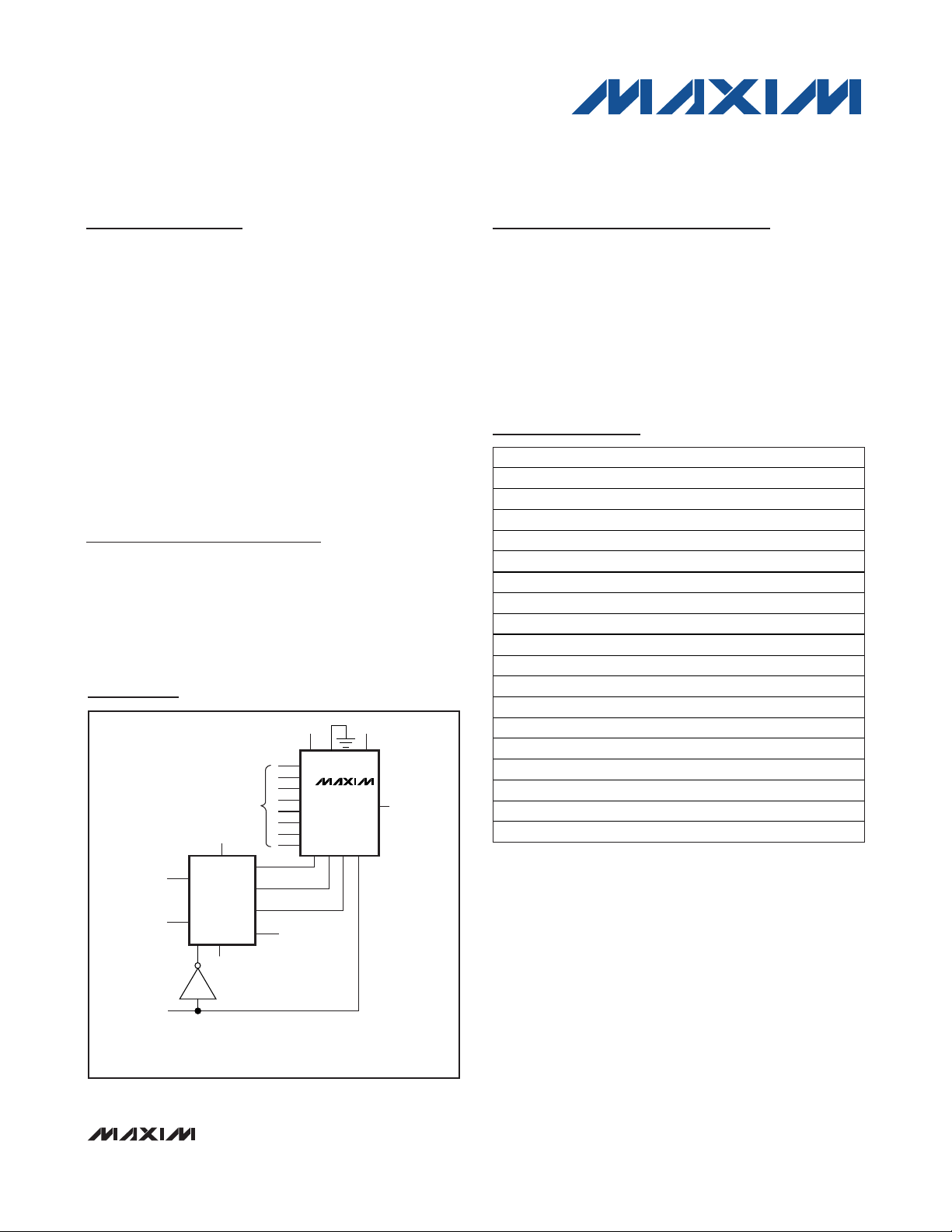
DG508A
Typical Operating Circuits
19-0028; Rev 4; 5/10
For pricing, delivery, and ordering information, please contact Maxim Direct at 1-888-629-4642,
or visit Maxim’s website at www.maxim-ic.com.
Devices are available in a lead(Pb)-free/RoHS-compliant package (except CERDIP). Specify lead-free by adding a plus (+)
to the part number when ordering.
*
Contact factory for dice specifications.
8-CHANNEL SEQUENTIAL MUX/DEMUX
Typical Operating Circuits continued at end of data sheet.
PART TEMP RANGE PIN-PACKAGE
DG508ACJ 0°C to +70°C 16 Plastic DIP
DG508ACWE 0°C to +70°C 16 Wide SO
DG508AC/D 0°C to +70°C Dice*
DG508ABK -20°C to +85°C 16 CERDIP
DG508ADJ -40°C to +85°C 16 Pla st ic DIP
DG508ADY -40°C to +85°C 16 Narrow SO
DG508AEWE -40°C to +85°C 16 Wide SO
DG508AAK -55°C to +125°C 16 CERDIP
DG508AMY/PR -55°C to +125°C 16 Narrow SO
DG509ACJ 0°C to +70°C 16 Plastic DIP
DG509ACWE 0°C to +70°C 16 Wide SO
DG509AC/D 0°C to +70°C Dice*
DG509ABK -20°C to +85°C 16 CERDIP
DG509ADJ -40°C to +85°C 16 Pla st ic DIP
DG509ADY -40°C to +85°C 16 Narrow SO
DG509AEWE -40°C to +85°C 16 Wide SO
DG509AAK -55°C to +125°C 16 CERDIP
DG509AMY/PR -55°C to +125°C 16 Narrow SO
Page 2
Monolithic CMOS Analog Multiplexers
2 _______________________________________________________________________________________
ABSOLUTE MAXIMUM RATINGS
ELECTRICAL CHARACTERISTICS
(V+ = 15V, V- = -15V, V
GND
= 0V, TA= +25°C, unless otherwise noted.)
Stresses beyond those listed under “Absolute Maximum Ratings” may cause permanent damage to the device. These are stress ratings only, and functional
operation of the device at these or any other conditions beyond those indicated in the operational sections of the specifications is not implied. Exposure to
absolute maximum rating conditions for extended periods may affect device reliability.
Voltage Referenced to V-
V+ .....................................................................................+44V
GND ................................................................................. +25V
Digital Inputs, V
S
and VD(Note 1)...................-2V to (V+ + 2V)
or 20mA, whichever occurs first
Current (any terminal, except S or D) .................................30mA
Continuous Current, S or D .................................................20mA
Peak Current, S or D (pulsed at 1ms, 10% duty cycle max) ..40mA
Continuous Power Dissipation (T
A
= +70°C)
Plastic DIP (derate 10.53mW/°C above +70°C) ...........842mW
Narrow SO (derate 8.70mWI°C above +70°C) .............696mW
Wide SO (derate 9.52mW/°C above +70°C).................762mW
CERDIP (derate 10.00mW/°C above +70°C)................800mW
Operating Temperature Ranges:
DG50_ACJ/CWE ..................................................0°C to +70°C
DG50_ABK........................................................-20°C to +85°C
DG50_ADJ/DY/EWE..........................................-40°C to +85°C
DG50_AAK/MY ...............................................-55°C to +125°C
Storage Temperature Range .............................-65°C to +150°C
Lead Temperature (soldering, 10s) .................................+300°C
Soldering Temperature (reflow)
PDIP, Wide SO, Narrow SO, CERDIP containing lead(Pb)..+240°C
PDIP, Wide SO, Narrow SO lead(Pb)-free ....................+260°C
DG508A/DG509A
Note 1: Signals on S_ or D_ exceeding V+ or V- are clamped by internal diodes. Limit forward-diode current to maximum current ratings
PARAMETER S YMBOL CONDITIONS
SWITCH
Analog Signal
Drain-Source OnResistance
Greatest Change
in Drain-Source
On-Resistance
Between Channels
Source OffLeakage Current
Drain Off-
DG508A
Leakage
Current
Drain On-
DG509A
DG508A
Leakage
Current
DG509A
V
R
R
-15 +15 -15 +15 V
ANALOG
VD = 10V,
I
S
VD = -10V,
I
S
max R
R
DS(ON)
VS = 10V, VD = -10V 0.002 0.5 0.002 1
= -10V, VD = 10V -0.5 -0.005 -1 -0.005
V
S
DS(ON)
DS(ON)
I
S(OFF)
Sequence each
switch on,
V
= 0.8V,
A_L
= 2.4V (Note 4)
V
A_H
R
DS(ON)
V
-10V
VEN = 0V
R
=
S 10V
DS(ON)
VD = 10V, VS = -10V 0.01 2 0.01 5
= -10V, VS = 10V -2 -0.015 -5 -0.015
V
I
D(OFF)
I
D(ON)
VEN = 0V
Sequence each
switch on,
V
= 0.8V
A_L
= 2.4V
V
A_H
(Note 2)
D
VD = 10V, VS = -10V 0.005 2 0.005 5
= -10V, VS = 10V -2 -0.008 -5 -0.008
V
D
V
= VD = 10V 0.015 2 0.015 5
S(all)
= VD = -10V -2 -0.03 -5 -0.03
V
S(all)
V
= VD = 10V 0.007 2 0.007 5
S(all)
V
= VD = -10V -2 -0.015 -5 -0.015
S(all)
= -200μA
= 200μA
DG508AA/M
DG509AA/M
DG508AD/E/B/C
DG509AD/E/B/C
MIN TYP MAX MIN TYP MA X
170 400 170 450
130 400 130 450
min
DS(ON)
6 6 %
UNITS
nA
nA
nA
Page 3
DG508A/DG509A
Monolithic CMOS Analog Multiplexers
_______________________________________________________________________________________ 3
ELECTRICAL CHARACTERISTICS (continued)
(V+ = 15V, V- = -15V, V
GND
= 0V, TA= +25°C, unless otherwise noted.)
PARAMETER S YMBOL CONDITIONS
LOGIC INPUT
Logic Input Current,
Input Voltage High
Logic Input Current,
Input Voltage Low
DYNAMIC
Multiplexer Switch ing
Break-Before-Make
Interval
Enable Turn-On Time t
Enable Turn-Off Time t
Off-Isolat ion OIRR
Source Off-Capacitance C
Drain OffCapacitanc
SUPPLY
Positive Supply Current I+ VEN = 2.4V, all VA_ = 0V or 2.4V 0.02 0.2 0.02 0.2 mA
Negative Supply Current I- VEN = 2.4V, all VA_ = 0V or 2.4V -0.1 -0.01 -0.1 -0.01 mA
Positive Supply Current
in Standby
Negative Supply Current
in Standby
Power-Supply Range for
Continuou s Operation
IDG508A 25 25
DGS09A
V
= 2.4V -10
I
AH
I
AL
t
transi tion
t
OPEN
ON(EN)
OFF(EN)
S(OFF)
C
D(OFF)
I+ V
I- V
V-, V+ (Notes 4, 5) ±4.5 ±18.0 ±4.5 ±18.0 V
A_
V
= 15V 0.006 10 0.006 10
A_
All VA_ = 0V
Figure 1 0.6 1. 0 0.6 1. 0 μs
Figure 3 0.2 0.2 μs
Figure 2 0.4 1.0 0.4 1.5 μs
Figure 2 0.2 0.7 0.2 1.0 μs
V
= 0V, RL= 1k, CL = l5pF,
EN
V
= 7V
S
RMS
VS = 0V, VEN = 0V, f = 140kHz 5 5 pF
VS = 0V, VEN = 0V, f = 140kHz
= 0V, all VA_ = 0V or 2.4V 0.02 0.2 0.02 0.2 mA
EN
= 0V, all V
EN
VEN = 2.4V -10
= 0V -10
V
EN
f = 500kHz (Note 3)
= 0V or 2.4V -0.1 -0.01 -0.1 -0.01 mA
A_
DG508AA/M
DG509AA/M
MIN TYP MA X MIN TY P MAX
-
-
-
68 68 dB
12 12
DG508AD/E/B/C
DG509AD/E/B/C
10 -0.002
10 -0.002
-10 -0.002
UNITS
μA
μA
pF
Page 4

DG508A/DG509A
Monolithic CMOS Analog Multiplexers
4 _______________________________________________________________________________________
ELECTRICAL CHARACTERISTICS
(V+ = 15V, V
GND
= 0V, TA= T
MIN
to T
MAX
, unless otherwise noted.)
Note 2: I
D(ON)
is leakage from driver into on switch.
Note 3: Off-isolation = 20log
V
S
= input to off switch,
VD= output due to VS.
Note 4: Electrical characteristics (such as on-resistance) change when power supplies other than ±15V are used.
Note 5: For designs requiring single 5V or dual ±5V operation, refer to Maxim’s improved MAX338 and MAX339. Minimum operating
voltage for DG508ADY/MY and DG509ADY/MY is ±9V.
PARAMETER S YMBOL CONDITIONS
SWITCH
Analog Signal
Range
Drain-Source OnResistance
Source Off-Leakage
Current
Drain OffLeakage
Current
Drain OnLeakage
Current
LOGI C I N P UT
Logic Input Current,
Input Voltage High
Logic Input Current,
Input Voltage Low
DG508A
DG509A
DG508A
DG509A
V
R
-15 +15 -15 +15 V
ANALOG
DS(ON)
I
VEN = 0V
S(OFF)
I
VEN = 0V
D(OFF)
I
D(ON)
I
AH
I
All VA_ = 0V
AL
DG508AA/M
DG509AA/M
MIN TYP MA X MIN TYP MAX
Sequence each
switch on,
V
= 0.8V,
A_L
V
= 2.4V
A_H
VD = 10V,
I
= -200μA
S
V
= -10V,
D
I
= 200μA
S
500 550
500 550
VS = 10V, VD = -10V +50 +50
= -10V, VD = -10V -50 -50
V
S
VD = 10V, VS = -10V +200 +100
= -10V, VS = -10V -200 -200
V
D
VD = 10V, VS = -10V +200 +100
= -10V, VS = -10V -100 -100
V
D
V
= VD = 10V +200 +100
Sequence each
switch on,
V
= 0.8V,
A_L
V
= 2.4V
A_H
(Note 2)
S(all)
= VD = -10V -200 -100
V
S(all)
V
= VD = 10V +100 +100
S(all)
= VD = -10V -100 -100
V
S(all)
VA_ = 2.4V -30 -30
VA_ = 15V +30 +30
VEN = 2.4V -30 -30
= 0V -30 -30
V
EN
DG508AD/E/B/C
DG509AD/E/B/C
UNITS
nA
nA
nA
μA
μA
IV I
S
IV I
D
Page 5

DG508A/DG509A
Monolithic CMOS Analog Multiplexers
_______________________________________________________________________________________ 5
Pin Descriptions
16
15
14
13
12
11
10
9
1
2
3
4
5
6
7
8
A0
A1
A2
GND
V+
S5
S6
S7
S8
TOP VIEW
DG508A
EN
V-
S3
S1
S2
S4
D
16
15
14
13
12
11
10
9
1
2
3
4
5
6
7
8
A0
A1
GND
V+
S1B
S2B
S3B
S4B
DB
DG509A
DIP/SO
EN
V-
S3A
S1A
S2A
S4A
DA
Pin Configurations
Functional Diagrams
V+
D
A2 A1 A0 EN
V- GND
S1
S2
S3
S4
S5
S6
S7
S8
DG508A CMOS
DECODE LOGIC
DG508A
8-CHANNEL SINGLE ENDED MULTIPLEXER
V+
DA
A1 A0 EN
V- GND
DB
S1A
S2A
S3A
S4A
S1B
S2B
S3B
S4B
DG509A CMOS
DECODE LOGIC
DG509A
DIFFERENTIAL 4-CHANNEL MULTIPLEXER
PIN
DG508A DG509A
DIP/ SO DI P/SO
1, 15, 16 —
— 1, 16 A0, A1 Address Input
2 2 EN Enable
3 3 V-
4–7 — S1–S4
— 4–7 S1A–S4A
8 — D
— 8, 9 DA, DB
9–12 — S8–S5
— 10–13 S4B–S1B
13 14 V+
14 15 GND Ground
NAME FUNCTION
A0, A2,
A1
Address Input
Negative-Supply Voltage
Input
Analog Inputs,
Bidirectional
Analog Inputs,
Bidirectional
Analog Outputs,
Bidirectional
Analog Outputs,
Bidirectional
Analog Inputs,
Bidirectional
Analog Inputs,
Bidirectional
Positive-Supply Voltage
Input
Page 6
DG508A/DG509A
Monolithic CMOS Analog Multiplexers
6 _______________________________________________________________________________________
Figure 1a. Switching-Time Test Circuit
DG508A
EN
V+
S1 -5V
SWITCH
OUTPUT
V
D
35pF
1kΩ
S2–S7
D
+15V
A0
A1
A2
GND
-15V
50Ω
LOGIC
INPUT
V-
Figure 2a. DG508A Enable-Time Test Circuit
DG509A
EN
V+
S1B -5V
SWITCH
OUTPUT
V
DS
35pF
1kΩ
S1A–S4A,
DA, S2B, S3B
DB
+15V
A0
A1
GND
-15V
50Ω
LOGIC
INPUT
V-
Figure 2b. DG509A Enable-Time Test Circuit
Figure 1b. Switching-Time Test Circuit
+2.4V +15V
DG508A
V+
S2–S7
V-
-15V
LOGIC
INPUT
EN S1 ±10V
A0
A1
A2
GND
50Ω
+2.4V +15V
DG509A
V+
S1A–S4A,
DA, S2B, S3B
S4B
V-
-15V
1MΩ
SWITCH
OUTPUT
V
DS
35pF
DB
EN S1 ±10V
S8
1MΩ
SWITCH
OUTPUT
V
D
35pF
LOGIC
INPUT
D
50Ω
A0
A1
GND
Page 7

DG508A/DG509A
Monolithic CMOS Analog Multiplexers
_______________________________________________________________________________________ 7
Figure 3. Break-Before-Make Test Circuit
t
open
t
transition
t
transition
t
OFF
(EN)
t
ON
(EN)
S8ON
3V
LOGIC INPUT
t
r
< 20ns
t
f
< 20ns
SWITCH
OUTPUT
V
D
(SEE FIG. 1)
TRANSITION
TIME
SWITCH
OUTPUT
V
D
(SEE FIG. 2)
TENABLE t
(ON) t(OFF)
TIME
SWITCH
OUTPUT
V
D
(SEE FIG. 3)
OPEN TIME
(B.B.M INTERVAL)
50%
0
V
S1
V
S8
0.8V
S1
V
0
V
S
V
S
50%
0V
0.9V
0
0.1V
0
0.8V
S8
0
0
S
1
ON
Figure 4. Timing Diagram for Figures 1, 2, and 3
Table 1a. DG508A Truth Table
Table 1b. DG509A Truth Table
X = Don’t care.
X = Don’t care.
+2.4V +15V
EN
LOGIC
INPUT
50Ω
A0, A1, (A2)
GND
DG508A
DG509A
AND DA
V-
-15V
ALL S
DB, D
+5V
1kΩ
A2 A1 A0 EN ON SWITCH
X X X 0 NONE
0001 1
0011 2
0101 3
0111 4
1001 5
1011 6
1101 7
1111 8
SWITCH
OUTPUT
V
D
35pF
A1 A0 EN ON SWITCH
X X 0 NONE
0011
0112
1013
1114
Page 8

DG508A/DG509A
Monolithic CMOS Analog Multiplexers
8 _______________________________________________________________________________________
Typical Operating
Circuits (continued)
PACKAGE TYPE PACKAGE CODE DOCUMENT NO.
16 Plastic DIP P16-1
21-0043
16 Wide SO W16-2
21-0042
16 Narrow SO S16-5
21-0041
16 CERDIP J16-3
21-0045
Package Information
For the latest package outline information and land patterns,
go to www.maxim-ic.com/packages
. Note that a “+”, “#”, or
“-” in the package code indicates RoHS status only. Package
drawings may show a different suffix character, but the drawing
pertains to the package regardless of RoHS status.
-15V
V+ V-GND
S1A
DIFFERENTIAL
ANALOG
INPUTS
(OUTPUTS)
+15V
CLOCK IN
RESET ENABLE
J
1/2MM747C73
CLOCK CLOCK
K
CLEAR GND
DIFFERENTIAL 4-CHANNEL SEQUENTIAL MUX/DEMUX
S2A
S3A
S4A
S1B
S2B
S3B
S4B
Q
Q
-15V
DG509A
A0
A1
N.C.
DA
DB
EN
J
1/2MM747C73
K
DIFFERENTIAL
ANALOG
OUTPUTS
(INPUTS)
Q
Q
Page 9
DG508A/DG509A
Monolithic CMOS Analog Multiplexers
Maxim cannot assume responsibility for use of any circuitry other than circuitry entirely embodied in a Maxim product. No circuit patent licenses are
implied. Maxim reserves the right to change the circuitry and specifications without notice at any time.
Maxim Integrated Products, 120 San Gabriel Drive, Sunnyvale, CA 94086 408-737-7600 _____________________
9
© 2010 Maxim Integrated Products Maxim is a registered trademark of Maxim Integrated Products, Inc.
Revision History
REVISION
NUMBER
4 5/10
REVISION
DATE
DESCRIPTION
Updated the “Drain-Source On-Resistance” parameter for both the TA = +25°C and
T
= T
MIN
to T
A
Deleted the QFN package from the Ordering Information, Absolute Maximum Ratings,
Pin Conf igurations, Pin Descriptions, and Package Information sections.
Added the DG508AMY/PR and DG509AMY/PR parts to the Ordering Information table. 1
conditions.
MAX
PAGES
CHANGED
2, 4
1, 2, 5, 8
 Loading...