

19-3926; Rev 0; 3/91
Quad, SPST Analog Switches
_______________General Description
The DG308A/DG309 are quad, single-pole-single-throw
(SPST) analog switches. The DG308A is normally open
(SPST, NO), while the DG309 is normally closed (SPST,
NC). Both parts feature fast switching speeds and low onresistance over the analog range. Other features include a
turn-on time under 120ns, a turn-off time under 90ns, and a
channel on-resistance of 60Ω. CMOS inputs provide
reduced input loading and very low leakage currents.
Both parts feature a 44V maximum breakdown voltage rating that allows 30V peak-to-peak switch-off blocking
capacity. The DG308A/DG309 can be used with split supplies (±5V to ±20V) or a single positive supply (+5V to
+30V), while retaining CMOS-logic-compatible inputs.
________________________Applications
Sample-and-Hold Circuits
Test Equipment
Communications Systems
PBX, PABX
Guidance and Control Systems
Heads-Up Displays
Military Radios
____________________________Features
♦ 60Ω r
DS(ON)
♦ Single/Bipolar-Supply Operation
♦ CMOS Logic Compatible
♦ Monolithic, Low-Power CMOS Design
______________Ordering Information
PART
DG308ACJ
DG308ACY
DG308ACK 0°C to +70°C
DG308AC/D 0°C to +70°C Dice*
DG308ADJ
DG308ADY
DG308ADK -40°C to +85°C
DG308AAK -55°C to +125°C 16 CERDIP**
DG309CJ
DG309CY
DG309CK 0°C to +70°C
DG309C/D 0°C to +70°C Dice*
DG309DJ
DG309DY
DG309DK -40°C to +85°C
DG309AK -55°C to +125°C 16 CERDIP**
* Contact factory for dice specifications.
** Contact factory for availability and processing to MIL-STD-883.
TEMP. RANGE PIN-PACKAGE
0°C to +70°C
0°C to +70°C
-40°C to +85°C 16 Plastic DIP
-40°C to +85°C
0°C to +70°C 16 Plastic DIP
0°C to +70°C
-40°C to +85°C 16 Plastic DIP
-40°C to +85°C
16 Plastic DIP
16 Narrow SO
16 CERDIP
16 Narrow SO
16 CERDIP
16 Narrow SO
16 CERDIP
16 Narrow SO
16 CERDIP
DG308A/DG309
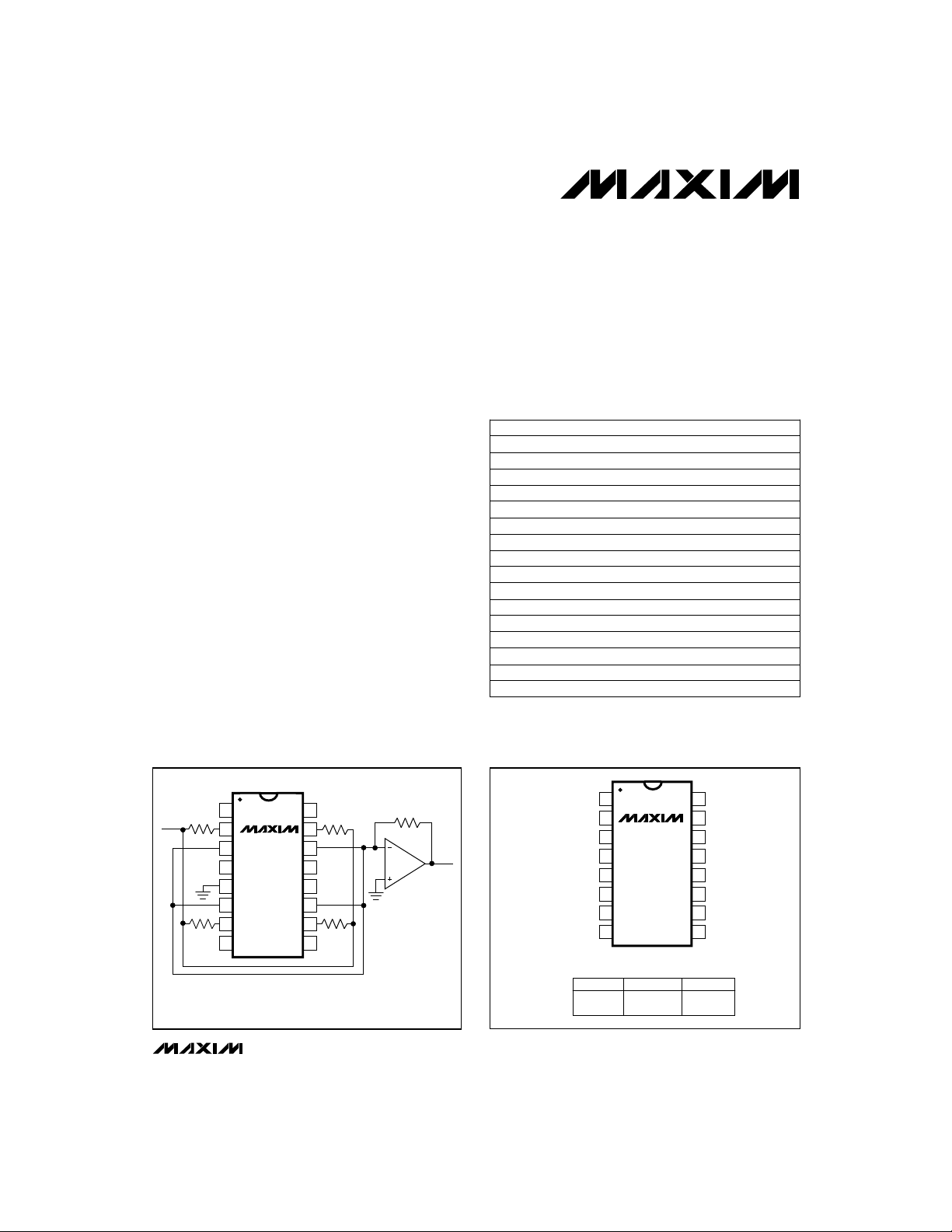
__________Typical Operating Circuit
VIN ±10V
* PINS 1, 8, 9, AND 16 ARE LOGIC-CONTROL INPUTS.
2
DG308A
3
-15V +15V
10k 20k
DG309
4
5
6
7
8
**
PROGRAMMABLE-GAIN AMPLIFIER
________________________________________________________________
1
**
5k
16
15
14
13
12
11
10
9
40k
5k
V
OUT
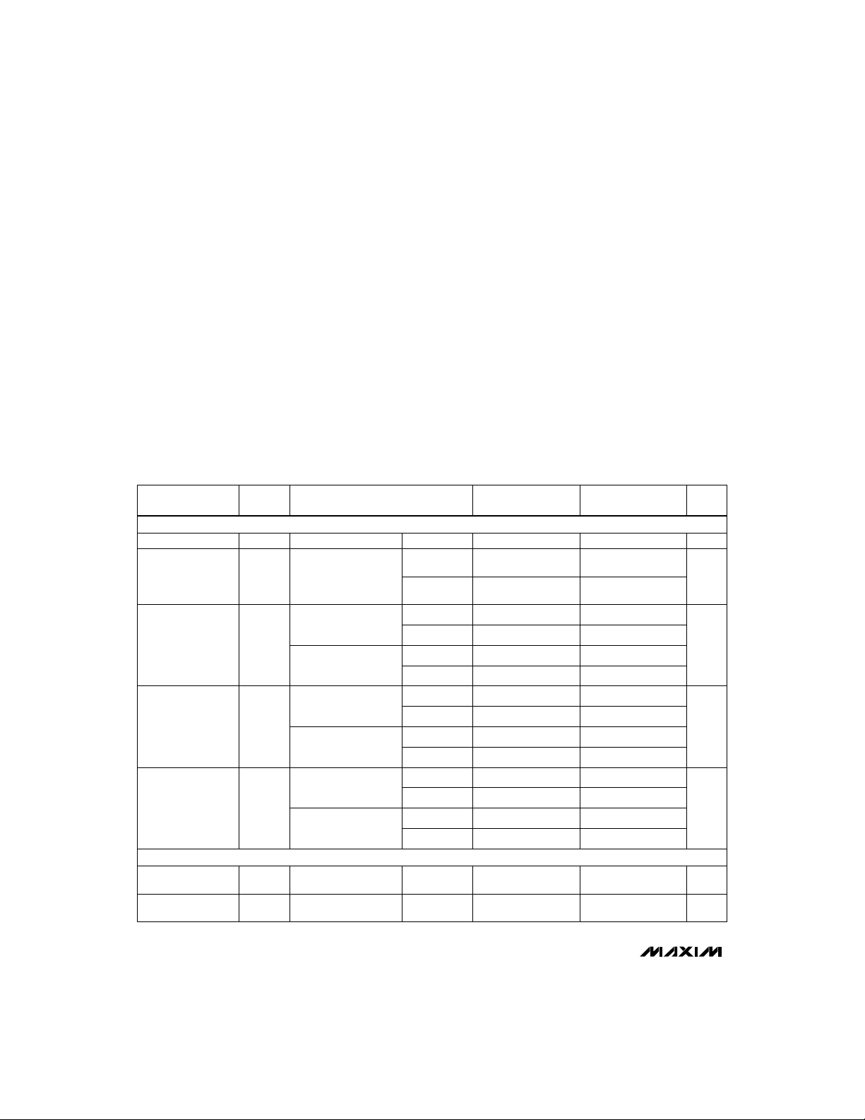
______Pin Configuration/Truth Table
TOP VIEW
IN1
1
2
D1
S1
3
4
V-
5
GND
6
S4
D4
7
IN4
8
TRUTH TABLE
LOGIC DG308A
0
1
DG308A
DG309
DIP/SO
OFF
ON
Maxim Integrated Products
IN2
16
D2
15
S2
14
13
V+ (SUBSTRATE)
N.C.
12
11
S3
10
D3
9
IN3
DG309
ON
OFF
1
For free samples & the latest literature: http://www.maxim-ic.com, or phone 1-800-998-8800
Quad, SPST Analog Switches
ABSOLUTE MAXIMUM RATINGS
Voltage Referenced to V-
V+ ....................................................................................+44V
GND.................................................................................+25V
Digital Inputs V
Current into Any Terminal (except S or D)..........................30mA
Continuous Current (S or D)................................................20mA
Peak Current (S or D)
(pulsed at 1ms, 10% duty cycle max) ............................70mA
Stresses beyond those listed under “Absolute Maximum Ratings” may cause permanent damage to the device. These are stress ratings only, and functional
operation of the device at these or any other conditions beyond those indicated in the operational sections of the specifications is not implied. Exposure to
absolute maximum rating conditions for extended periods may affect device reliability.
, VD................(V- - 2V) to (V+ + 2V) or 20mA,
S
whichever occurs first
Continuous Power Dissipation (TA= +70°C) (Note 1)
Plastic DIP (derate 10.53mW/°C above +70°C)............842mW
Narrow SO (derate 8.70mW/°C above +70°C) .............696mW
CERDIP (derate 10.00mW/°C above +70°C)................800mW
Operating Temperature Ranges
DG308AC_/DG309C_.........................................0°C to +70°C
DG308AD_/DG309D_......................................-40°C to +85°C
DG308AAK/DG309AK...................................-55°C to +125°C
Storage Temperature Range.............................-65°C to +150°C
Lead Temperature (soldering, 10sec).............................+300°C
DG308A/DG309
ELECTRICAL CHARACTERISTICS
(V+ = 15V, V- = -15V, TA= T
SWITCH
Analog Signal Range
Drain-Source
On-Resistance
Source-Off
Leakage Current
Drain-Off
Leakage Current
Drain-On
Leakage Current
INPUT
Input Current with
Input Voltage High
Input Current with
Input Voltage Low
SYMBOLPARAMETER
ANALOG
r
DS(ON)
I
S(OFF)
I
D(OFF)
I
D(ON)
INH
INL
to T
MIN
, unless otherwise noted.) (Note 2)
MAX
VIN= 11V (DG308A),
VIN= 3.5V (DG309),
IS= 1mA,
VD= 10V or -10V
VIN= 3.5V (DG308A),
VIN= 11V (DG309),
VS= 14V, VD= -14V
VIN= 3.5V (DG308A),
VIN= 11V (DG309),
VS= -14V, VD= 14V
VIN= 3.5V (DG308A),
VIN= 11V (DG309),
VS= 14V, VD= -14V
VIN= 3.5V (DG308A),
VIN= 11V (DG309),
VS= -14V, VD= 14V
VIN=11V (DG308A),
VIN= 3.5V (DG309),
VS= VD= +14V
VIN= 11V (DG308A),
VIN= 3.5V (DG309),
VS= VD= -14V
VIN= 15V
VIN= 0V
CONDITIONS
TA= +25°C
= +25°C,
T
A
T
MIN
TA= T
MAX
TA= +25°C
TA= T
MAX
TA= +25°C
TA= T
MAX
TA= +25°C
TA= T
MAX
TA= +25°C
TA= T
MAX
TA= +25°C
TA= T
MAX
TA= +25°C
TA= T
MAX
TA= +25°C,
T
MAX
TA= +25°C,
T
MAX
DG30_AK
MIN TYP MAX
60 100
95 150
-1 0.1 1
-100 100
-1 -0.1 1
-100 100
-1 0.1 1
-100 100
-1 0.1 1
-100 100
-2 0.1 2
-200 200
-2 0.1 2
-200 200
DG30_C/D
MIN TYP MAX
-15 15
60 100
80 125
-5 0.1 5
-100 100
-5 0.1 5
-100 100
-5 0.1 5
-100 100
-5 0.1 5
-100 100
-5 0.1 5
-200 200
-5 0.1 5
-200 200
-1 0.001 1
-1 0.001 1
UNITS
V-15 15V
Ω
nA
nA
nA
µA-1 0.001 1I
µA-1 -0.001 1I
2 _______________________________________________________________________________________
Quad, SPST Analog Switches
ELECTRICAL CHARACTERISTICS (continued)
(V+ = 15V, V- = -15V, TA= T
PARAMETER SYMBOL
SUPPLY
Positive Supply
Current
Negative Supply
Current
DYNAMIC
Turn-On Time t
Off Isolation
(Note 3)
Source-Off
Capacitance
Drain-Off
Capacitance
Channel-On
C
Capacitance
Note 1: All leads are soldered or welded to the PC board.
Note 2: The algebraic convention where the most negative value is a minimum and the most positive value a maximum is used in
this data sheet.
Note 3: Off isolation = 20log10 V
to T
MIN
I+
I-
ON
OFF
OIRR 78 dB
C
S(OFF)
C
D(OFF)
D(ON) +
C
S(ON)
, unless otherwise noted.) (Note 2)
MAX
All channels on or off,
VIN= 0V or 15V
TA= T
MAX
All channels on or off,
VIN= 0V or 15V
TA= T
MAX
Figure 1
Figure 1
GEN
= 0V, R
GEN
= 0Ω
VIN= 0V (DG308A), VIN= 15V (DG309),
ZL= 75Ω, VS= 2V
, f = 500kHz
p-p
VIN= 0V (DG308A), VIN= 15V (DG309),
f = 140kHz, VS= 0V
VIN= 0V (DG308A), VIN= 15V (DG309),
f = 140kHz, VS= 0V
VIN= 0V (DG308A), VIN= 15V (DG309),
VD= VS= 0V
, VD= output, VS= input to off switch.
D/VS
DG30_AK
MIN TYP MAX
-10 0.001 10TA= +25°C
DG30_C/D
MIN TYP MAX
-100 0.001 100
100
-100 -0.001 100-10 -0.001 10TA= +25°C
-100
130 200 ns
90 150 ns
-100
130 200
90 150Turn-Off Time t
-10Charge Injection Q -10 pCCL= 0.01µF, V
78
11 pF
8 pF
27 pF
11
8
27
100
UNITSCONDITIONS
DG308A/DG309
µA
µA
LOGIC
INPUT IN1
< 20ns
t
r
t
< 20ns
f
SWITCH
INPUT
SWITCH
OUTPUT VO
50%
OV
V
S
0.9V
0V
t
ON
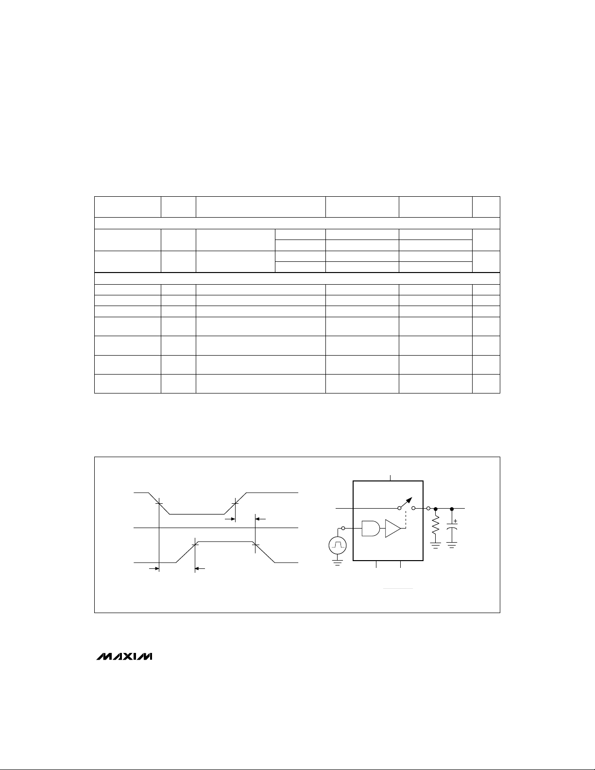
Figure 1. Switching-Time Test Circuit
_______________________________________________________________________________________ 3
+15V
V+
SWITCH
INPUT
VS = +3V
t
OFF
O
0.9V
O
LOGIC
INPUT
IN1
GND 0VV-
-15V
R
= V
V
O
S
RL + r
D1S1
R
L
1k
(REPEAT TEST FOR S2, S3, AND S4)
L
DS(ON)
C
35pF
L
SWITCH
OUTPUT
V
O
Quad, SPST Analog Switches
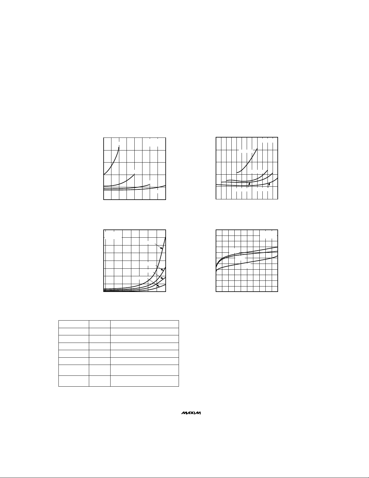
__________________________________________Typical Operating Characteristics
(TA = +25°C, unless otherwise noted.)
DRAIN-SOURCE ON-RESISTANCE
vs. DRAIN VOLTAGE & POWER SUPPLIES
500
V+ = 5V
400
TA = +25°C
V- = GND
DG308A309 TOC01
DRAIN-SOURCE ON-RESISTANCE
vs. DRAIN VOLTAGE & POWER SUPPLIES
250
200
V+ = ±5V
TA = +25°C
DG308A309 TOC04
300
(Ω)
DS(ON)
r
200
DG308A/DG309
100
0
0
V+ = 10V
V+ = 15V
510
VD (V)
15
V+ = 20V
20
POWER-SUPPLY CURRENT
AND VOLTAGE vs. TEMPERATURE
800
TA = +25°C
700
V- = GND
600
500
(nA)
400
SUPPLY
I
300
200
100
0
-50 12525-25 0 7550 100
TEMPERATURE (°C)
V+ = 44V
V+ = 30V
V+ = 10V
V+ = 5V
DG308A309 TOC02
_____________________Pin Description
PIN
FUNCTIONNAME
Logic Control InputsIN1–IN41, 8, 9, 16
Drain OutputD1–D42, 7, 10, 15
Source InputS1–S43, 6, 11, 14
Negative Supply Voltage InputV-4
GroundGND5
N.C.12
Maxim cannot assume responsibility for use of any circuitry other than circuitry entirely embodied in a Maxim product. No circuit patent licenses are
implied. Maxim reserves the right to change the circuitry and specifications without notice at any time.
4
___________________Maxim Integrated Products, 120 San Gabriel Drive, Sunnyvale, CA 94086 (408) 737-7600
No Connect. Not internally
connected.
Positive Supply Voltage Input.
V+13
Connected to substrate.
The DG308A/DG309 switch positive analog signals while
using a single positive supply, allowing use in applications where only one supply is available. The disadvantages of using a single supply are slower switching
speed and increased r
Current and Voltage vs. Temperature
typical curve for a single-supply design. As stated in the
Absolute Maximum Ratings, the analog voltage should
not go above or below the supply voltages, which are V+
and 0V in single-supply operation.
150
(Ω)
V+ = ±12V
VD (V)
V+ = ±10V
V+ = ±15V
0
51015
DS(ON)
r
100
50
0
-15
-10 -5
LEAKAGE CURRENTS vs.
ANALOG VOLTAGE
(pA)
D
, I
S
I
20
10
I
0
-10
-20
-30
S(OFF)
I
D(OFF)
-6 0
-12
V
ANALOG
I
D(ON)
(V)
TA = +25°C
= ±15V
V
CC
6
DG308A309 TOC03
12
__________Applications Information
. The
DS(ON)
Power-Supply
graph shows the
© 1991 Maxim Integrated Products Printed USA is a registered trademark of Maxim Integrated Products.
 Loading...