

Page 1

78M6618 PDU1 Evaluation Board
User Manual
November 2011
Rev 3
UM_6618_022
Page 2

78M6618 PDU1 Evaluation Board User Manual UM_6618_022
Maxim cannot assume responsibility for use of any circuitry other than circuitry entirely embodied in a Maxim product. No circuit
patent licenses are implied. Maxim reserves the right to change the circuitry and specifications without notice at any time.
Maxim Integrated Products, 120 San Gabriel Drive, Sunnyvale, CA 94086 408- 737- 7600
2011 Maxim Integrated Products Maxim is a registered trademark of Maxim Integrated Products.
Page 3

UM_6618_022 78M6618 PDU1 Evaluation Board User Manual
Table of Contents
1 Introduction.................................................................................................................................... 5
1.1 Package Contents................................................................................................................. 5
1.2 System Requirements ........................................................................................................... 5
1.3 Safety and ESD Notes .......................................................................................................... 6
1.4 Firmware Demo Code Introduction ........................................................................................ 6
1.5 Testing the Evaluation Board Prior to Shipping ...................................................................... 6
2 Installation ..................................................................................................................................... 7
2.1 USB Connection and Driver Installation ................................................................................. 8
2.2 Connecting the External DC Supply ...................................................................................... 8
2.3 Confirm COM Port Mapping .................................................................................................. 9
2.4 Verify Serial Connection to the PC ...................................................................................... 10
2.5 Connect the AC Source and Load ....................................................................................... 12
3 Circuit Description and Theory of Operation ............................................................................. 13
3.1 78M6618 ............................................................................................................................ 13
3.2 Voltage Regulators ............................................................................................................. 13
3.3 Input Signal Conditioning .................................................................................................... 14
3.4 Relay Control ...................................................................................................................... 14
3.5 Theory of Operation ............................................................................................................ 14
3.5.1 78M6618 Operation ................................................................................................... 14
3.5.2 Voltage and Current Measurement ............................................................................ 14
4 In-Circuit Emulator (ICE) Adaptor ............................................................................................... 17
5 Schematics, Bill of Materials, and PCB Layouts ........................................................................ 18
5.1 78M6618 PDU1 Evaluation Board Schematics .................................................................... 18
5.2 78M6618 PDU1 Evaluation Board Bill of Materials .............................................................. 22
5.3 78M6618 PDU1 Evaluation Board PCB Layouts.................................................................. 25
6 Ordering Information ................................................................................................................... 26
7 Contact Information ..................................................................................................................... 26
Appendix A - 78M6618 PDU1 Board with CTs .................................................................................... 27
A.1 78M6618 PDU-CT Evaluation Board ................................................................................... 27
A.2 78M6618 PDU-CT Evaluation Board Schematics ................................................................ 28
A.3 78M6618 PDU-CT Evaluation Board Bill of Materials .......................................................... 32
A.4 78M6618 PDU-CT Evaluation Board PCB Layouts .............................................................. 34
Appendix B – 78M6618 PDU1 Version 1 (Single-Ended Shunt) ......................................................... 36
Revision History .................................................................................................................................. 37
Rev 3 3
Page 4

78M6618 PDU1 Evaluation Board User Manual UM_6618_022
Figures
Figure 1: 78M6618 PDU1 Connections .................................................................................................... 7
Figure 2: Serial Port Verification Screen ................................................................................................. 12
Figure 3: Differential PDU Block Diagram............................................................................................... 13
Figure 4: PCB Parasitic Resistance ....................................................................................................... 15
Figure 5: Differential Amplifier and Current Sense Resistor .................................................................... 15
Figure 6: Detail View of Differential Amplifiers ........................................................................................ 16
Figure 7: ICE Adaptor ............................................................................................................................ 17
Figure 8: 78M6618 ICE Adaptor Attachment .......................................................................................... 17
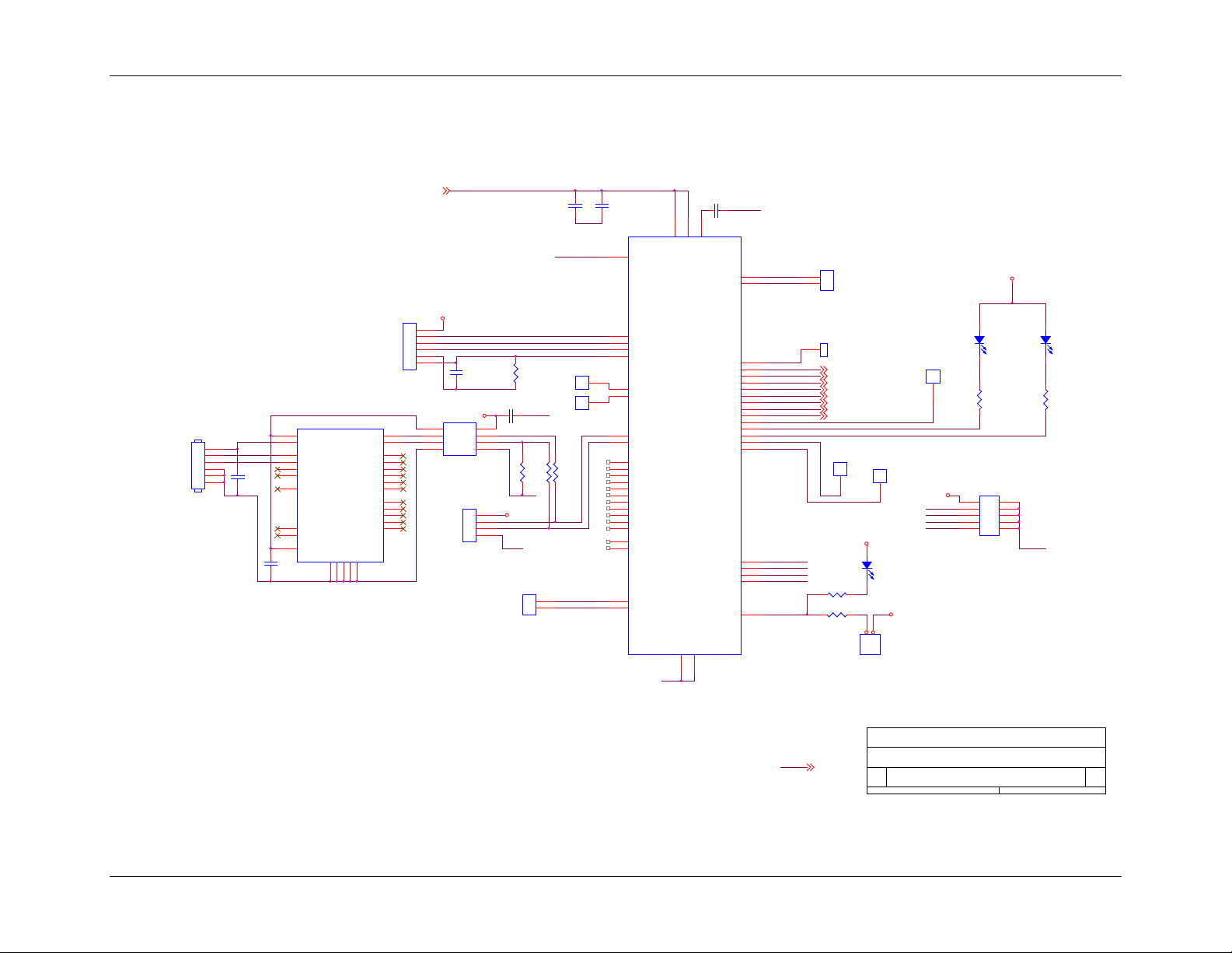
Figure 9: 78M6618 PDU1 Evaluation Board Electrical Schematic (1 of 4) ............................................... 18
Figure 10: 78M6618 PDU1 Evaluation Board Electrical Schematic (2 of 4) ............................................. 19
Figure 11: 78M6618 PDU1 Evaluation Board Electrical Schematic (3 of 4) ............................................. 20
Figure 12: 78M6618 PDU1 Evaluation Board Electrical Schematic (4 of 4) ............................................. 21
Figure 13: 78M6618 PDU1 Evaluation Board PCB Top View ................................................................. 25
Figure 14: 78M6618 PDU1 Evaluation Board PCB Power View.............................................................. 25
Figure 15: 78M6618 PDU1 Evaluation Board PCB GND View ................................................................ 25
Figure 16: 78M6618 PDU1 Evaluation Board PCB Bottom View ............................................................ 25
Figure 17: 78M6618 PDU-CT Evaluation Board ..................................................................................... 27
Figure 18: 78M6618 PDU-CT Evaluation Board Electrical Schematic (1 of 4) ......................................... 28
Figure 19: 78M6618 PDU-CT Evaluation Board Electrical Schematic (2 of 4) ......................................... 29
Figure 20: 78M6618 PDU-CT Evaluation Board Electrical Schematic (3 of 4) ......................................... 30
Figure 21: 78M6618 PDU-CT Evaluation Board Electrical Schematic (4 of 4) ......................................... 31
Figure 22: 78M6618 PDU-CT Evaluation Board PCB Top View.............................................................. 34
Figure 23: 78M6618 PDU-CT Evaluation Board PCB Bottom View......................................................... 35
Tables
Table 1: COM Port Setup Parameters .................................................................................................... 10
Table 2: 78M6618 PDU1 Evaluation Board Bill of Materials ................................................................... 22
Table 3: 78M6618 PDU-CT Evaluation Board Bill of Materials ................................................................ 32
4 Rev 3
Page 5
UM_6618_022 78M6618 PDU1 Evaluation Board User Manual
Teridian is a trademark of Maxim Integrated Products, Inc.
Windows and Windows XP are r egistered trademarks of M icrosoft Corp.
1 Introduction
The Teridian™ 78M6618 PDU1 evaluation board is an example of a low-cost power distribution unit
(PDU) utilizing the 78M6618 system-on-chip (SoC). The 78M6618 monitors the AC line voltage and eight
load currents, and controls switching of eight internal load relays. The embedded firmware calculates the
RMS line voltage and RMS load currents, watts, VAs, VARs, and power factor. The real-time data is
transmitted to a PC via a USB interface for display in a Windows
The 78M6618 UART interface is used as the communications link to an on-board isolated USB interface
IC.
®
-based graphical user interface (GUI).
Included with the 78M6618 PDU1 is a Windows-based GUI for simplified access to the following
measurement data and controls:
• RMS voltage and current
• Real, apparent, and reactive power and power factor
• Accumulated energy usage and expense tracking
• Line frequency
• Minimum and peak parameter tracking
• Alarm indicators
• Programmable alarm thresholds
• Internal load relay (16A) control
This document describes the evaluation board with “78M6618 PDU1_DIFF” imprinted on the board. This
board is a complete replacement for (and obsoletes) the earlier 78M6618 PDU1 evaluation board.
Refer to the GUI User Guide for information about the GUI.
1.1 Package Contents
The 78M6618 PDU1 evaluation kit includes:
• 78M6618 PDU1_DIFF evaluation board
• Universal AC to 12 V DC power supply with international plug adapters
• ICE Adaptor board
• USB A/B cable
1.2 System Requirements
The 78M6618 PDU1 GUI requires use of a PC with the following features:
• PC (1 GHz, 1 GB) with Microsoft Windows 7, Windows XP® or Win2000, equipped with USB port
• Minimum 1024 x 768 video display resolution
Rev 3 5
Page 6

78M6618 PDU1 Evaluation Board User Manual UM_6618_022
1.3 Safety and ESD Notes
EXERCISE CAUTION WHEN LIVE AC VOLTAGES ARE PRESENT!
Standard ESD precautions must be taken when handling electronic equipment. The
78M6618 PDU1 contains ESD protected interfaces.
Do not connect test equipment, ICE emulators or external development boards directly to the
78M6618 hardware. Damage to the 78M6618 PDU1 and external equipment will occur due to the
78M6618’s “high side” reference topology. The 78M6618’s V3P3 (i.e., “high side”) is connected
directly to Neutral (Earth Ground) and the ground is 3.3V below neutral, creating a ground
reference disparity with any properly grounded external equipment. Also, reversing the line and
neutral connections at the inlet would place the board’s ground reference at the AC line voltage.
Always use the isolated USB interface for connecting to a PC. Contact the factory for instructions
on connecting other types of test equipment.
The board components and firmware settings are designed to operate with the following nominal AC
electrical ranges:
Voltage Current Line Frequency
110-240 VAC 20A Max 46-64 Hz
1.4 Firmware Demo Code Introduction
The Firmware Demo Code provides the following features:
• Basic energy measurement data such as Watts, Volts, current, VAR, VA, phase angle, power factor,
accumulated energy, frequency, date/time, and various alarm statuses.
• Control of alarm thresholds, calibration coefficients, temperature compensation, etc.
There are two means to facilitate performance evaluation between the user at the PC host and the
firmware code in the 78M6618 PDU1 evaluation board:
• The graphical user interface (GUI). For information about the GUI, refer to the GUI User Guide.
• The Command Line Interface (CLI) via HyperTerminal or comparable terminal emulator on a different
operating system. For information about the CLI, see the Firmware Description Document.
The 78M6618 PDU1 evaluation board is shipped with demonstration code loaded in the 78M6618 device
and included on the CD. The code revision can be verified by entering the command >i via the command
line interface. Firmware for the Demo Unit can be updated using either the Teridian TFP2 or an in-circuit
emulator such as Signum Systems ADM51 (
www.signum.com ).
1.5 Testing the Evaluation Board Prior to Shipping
Before every 78M6618 PDU1 evaluation board is shipped, the following procedures have been performed
at the factory:
• Full Calibration – Precise energy source equipment is used to calibrate the current and voltage. The
temperature is also calibrated at the same time.
• Accuracy Test – This “bench” level test ensures the energy measurement accuracy is within +/-0.5%.
6 Rev 3
Page 7
UM_6618_022 78M6618 PDU1 Evaluation Board User Manual
Outlet 2
Outlet 8
Outlet 7
DC Power Plug
(J48)
AC Inlet (J4)
Outlet 6
Outlet 4
Outlet 5
Outlet 3
Outlet 1
Connect the USB Port
(J47) to the Host PC
2 Installation
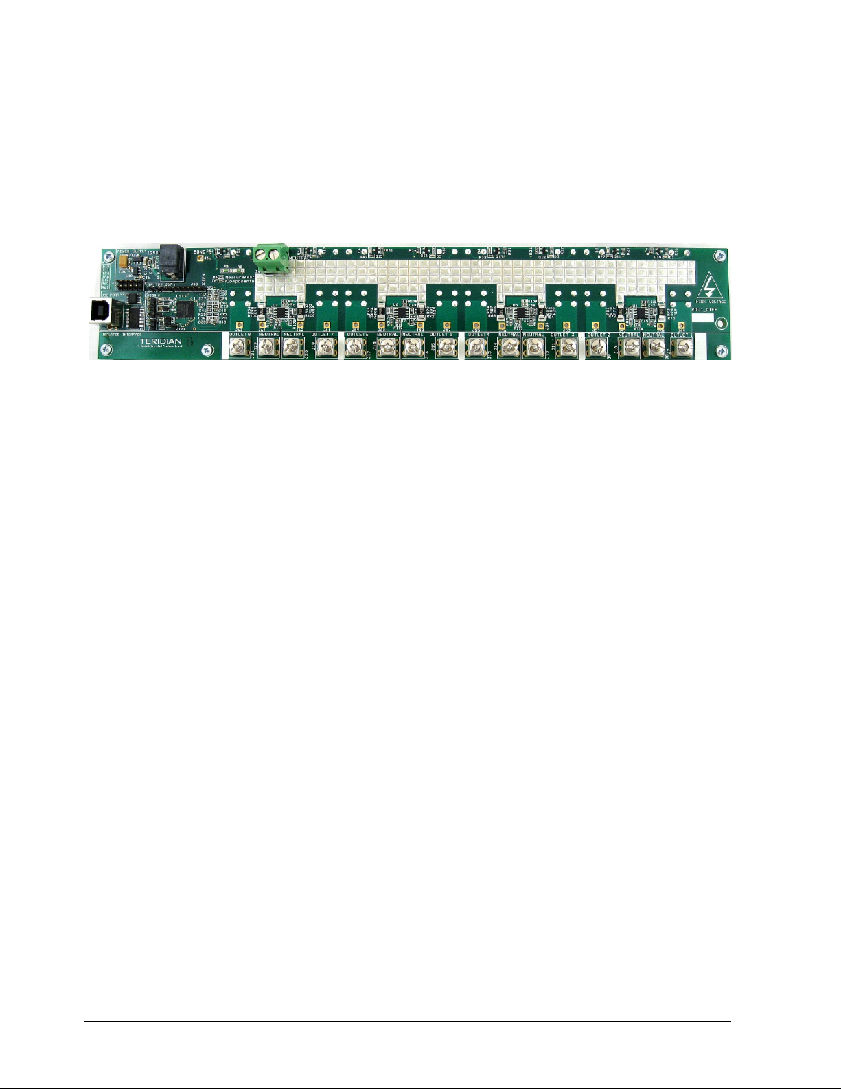
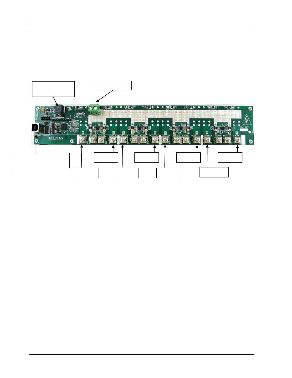
Figure 1 shows the basic connections to the 78M6618 PDU1 Evaluation Board. DC power is supplied to
the PDU1 through the DC power jack (J48). The USB cable provides an electrically isolated
communications link between the host PC and the PDU1 as well as power to the USB controller on the
Evaluation Board. The AC input to the PDU is connected via the terminal block J4. The PDU1 has eight
outlets that connect to the loads to be measured. Screw terminals are provided to make the line and
neutral connections to the loads.
Figure 1: 78M6618 PDU1 Connections
Rev 3 7
Page 8

78M6618 PDU1 Evaluation Board User Manual UM_6618_022
2.1 USB Connection and Driver Installation
This evaluation kit includes an isolated USB interface for serial communications with a PC. The FTDI USB
controller IC FT232R performs the USB functions. The FTDI Windows driver presents a virtual COM port
for enabling serial communications. Control of the 78M6618-PDU-1 can be managed using either a
terminal emulation program or using the supplied Windows Dashboard GUI. The FTDI Windows driver is
a certified driver for Windows 2000 and XP.
Because the USB interface is USB powered, the USB driver installation can be completed with no other
DC power supplied to the evaluation board.
1. Connect a USB AB cable between the host PC and the evaluation board.
2. Upon attaching the 78M6618-PDU-1 to the PC, the Found New Hardware Wizard automatically
launches and installs the appropriate driver files. If your PC does not find the FTDI driver files on its
local hard disk drive, locate and reference the FTDI USB Driver and Utilities subdirectory on the CD.
The FT232R controller is powered from the USB cable and is active even when no AC power is
applied to the 78M6618-PDU-1.
Note: If an older FTDI driver has been previously installed, it is recommended to remove the older
version before installing this newer FTDI driver. Execute the ftdiClean.exe utility from the FTDI
USB Driver and Utilities subdirectory.
For FTDI driver support on other operating systems, please check FTDI’s website at
(http://www.ftdichip.com/FTDrivers.htm).
2.2 Connecting the External DC Supply
An external DC supply is provided for operation of the evaluation board. Follow these steps to connect
the 78M6618 PDU1 with the external DC supply:
1. Select the appropriate plug for the AC adapter and snap it into place.
2. Connect the DC cable of the 12V AC adapter to J48.
3. Plug the AC adapter into an appropriate outlet.
8 Rev 3
Page 9
UM_6618_022 78M6618 PDU1 Evaluation Board User Manual
PDU-1 COM Port:
2.3 Confirm COM Port Mapping
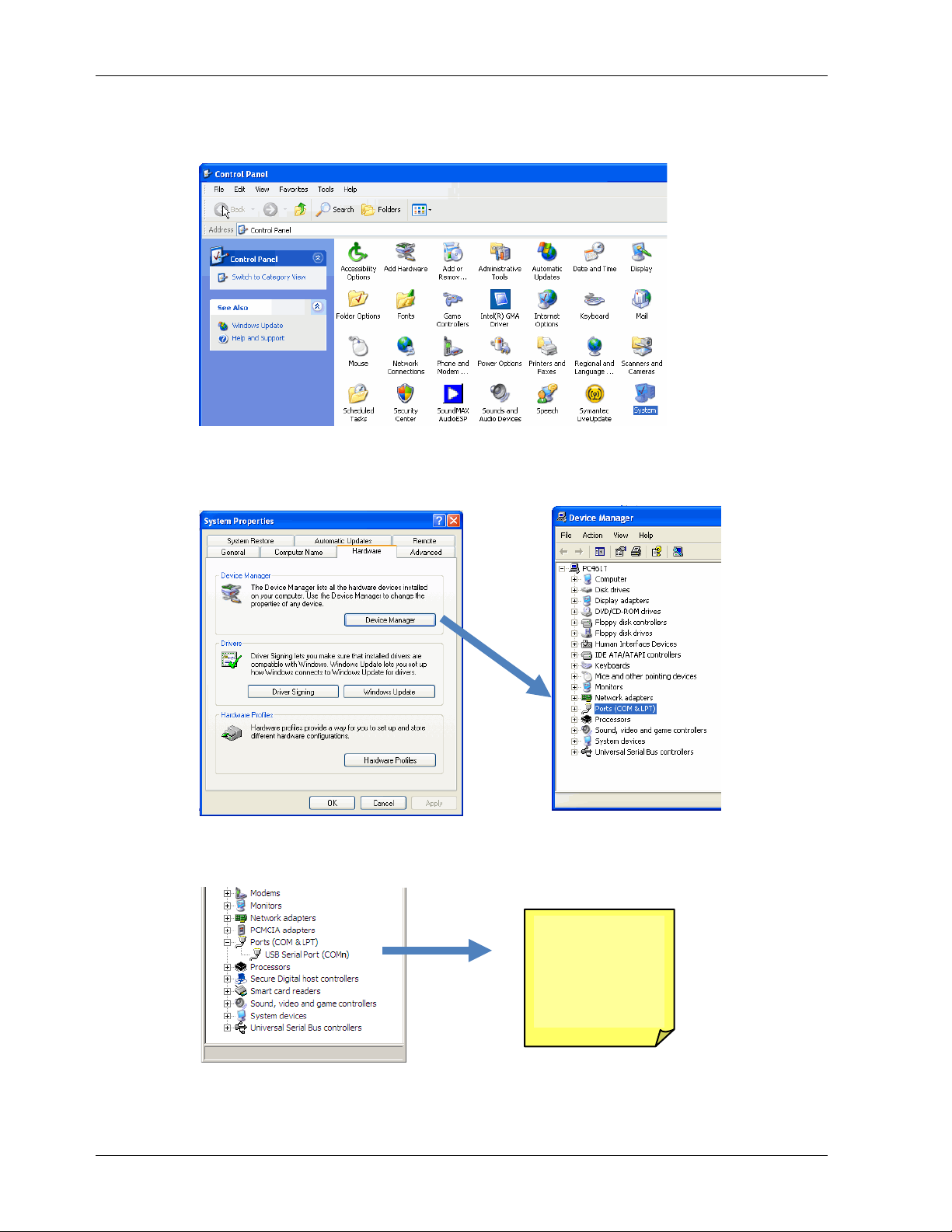
1. Launch the Control Panel and click on the System icon.
2. The System Properties screen appears. Click on the Hardware tab. Click on Device Manager.
Under Ports (COM & LPT), look for the USB Serial Port assignment.
3. Take note of the COM port assignment for the USB Serial Port.
Rev 3 9
Page 10
78M6618 PDU1 Evaluation Board User Manual UM_6618_022
Select
COM Port
2.4 Verify Serial Connection to the PC
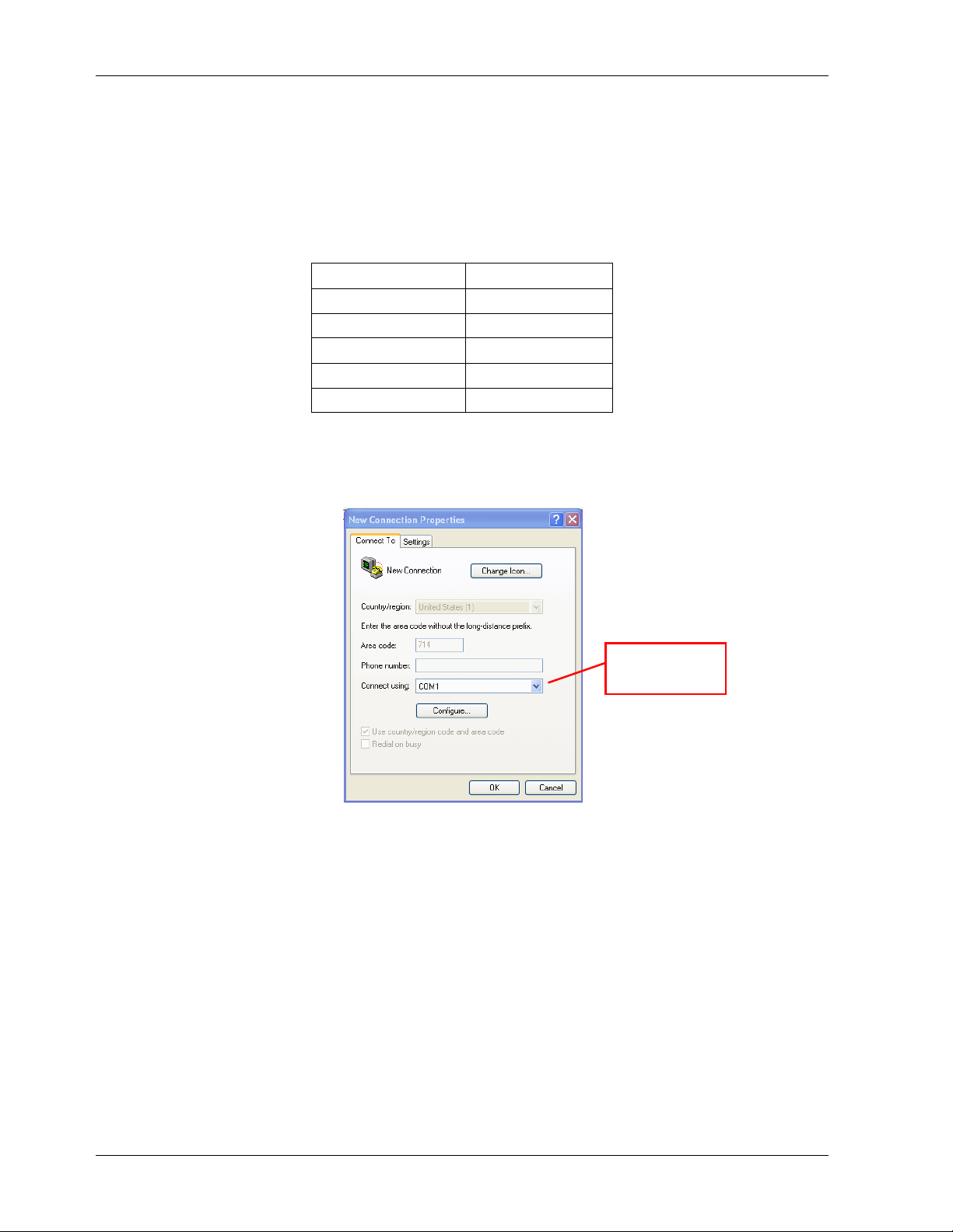
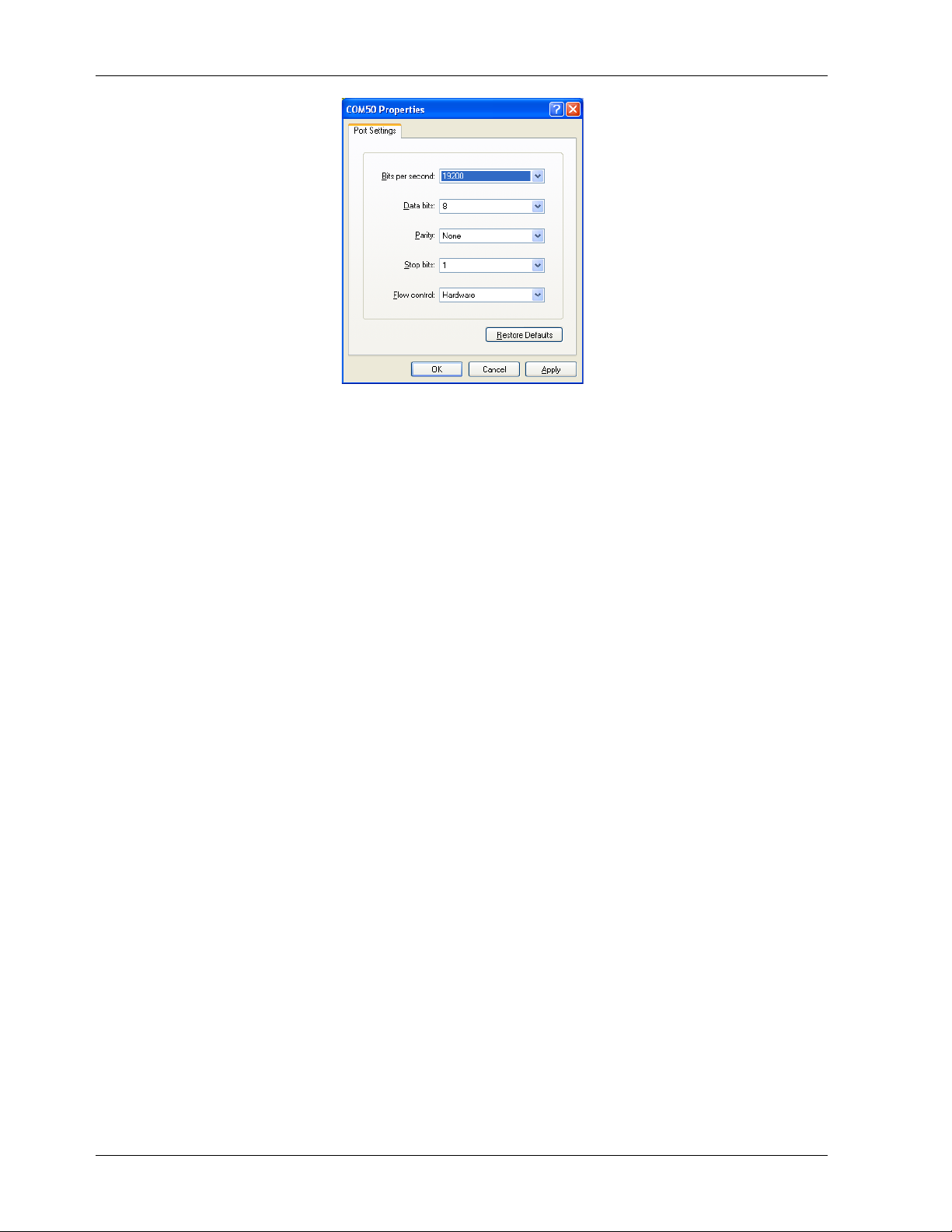
After connecting the USB cable from the 78M6618-PDU-1 to the host PC and powering the PDU board
with the 12VDC adapter, start the HyperTerminal application (or another suitable communication
program) to create a session using the communication parameters shown in Table 1. The firmware
installed in your board may use a different COM port setup than what is shown here. Refer to the
Firmware Description Document provided with your board for the correct setup for your firmware.
Table 1: COM Port Setup Parameters
Setup Parameter 78M6618
Port speed (baud) 38400
Data bits 8
Parity None
Stop bits 1
Flow control None
HyperTerminal can be found in Windows by selecting Start All Programs Accessories
Communications HyperTerminal. The connection parameters are configured by selecting File
Properties. The New Connection Properties menu appears.
Select the appropriate COM port and click Configure. The COMn Properties menu appears.
10 Rev 3
Page 11
UM_6618_022 78M6618 PDU1 Evaluation Board User Manual
Note that port parameters can only be adjusted when the connection is not active. It may be necessary to
click the Disconnect Button (shown below) to disconnect the port.
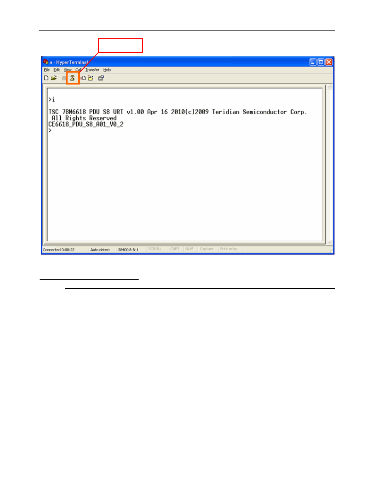
When the terminal emulation program has connected to the correct USB COM port, verify operation of the
PDU by pressing the “Enter” key on the PC. The evaluation board should respond with a “>” prompt. You
should also be able to identify the firmware version programmed into your board
If communication is not established with the evaluation board, check the following:
1. Make sure that 12VDC is supplied to the board through J48.
2. Make sure that the terminal emulation program is using the correct COM port.
3. Check the serial port configuration against the configuration given in the Firmware Description
Document.
Rev 3 11
Page 12
78M6618 PDU1 Evaluation Board User Manual UM_6618_022
If the FTDI device driver did not install properly, there would be no assigned COM port
Disconnect
Figure 2: Serial Port Verification Screen
FTDI COM Port Trouble-Shooting
number for the FTDI controller. Repeat the USB Driver Installation, see Section 2.1.
Microsoft Windows may associate a Ball Point device to the FTDI USB controller. When this
occurs a FTDI device COM port assignment is available via HyperTerminal but there is no
communications data. Verify if a Ball Point device has been added to the “Human Interface
Devices” via the Device manager. Refer to Section 2.3 for access to the Device Manager. If
a Ball Point device exists, delete it and unplug and replug the evaluation board’s USB cable.
2.5 Connect the AC Source and Load
Connect the desired AC source to the terminal block J4. Be sure to observe the correct connections for
line and neutral as they are designated on the silk screen. Terminal block J4 accepts bare wires size
24AWG to 10AWG. Be sure to select wire gauge appropriate to the total load to be applied to the board,
and make sure that the screws are tightened for good electrical connection and wire retention.
The loads to be controlled and metered are connected to the screw terminals J7-J22 that are located on
the bottom edge of the board. These terminals can accept bare wire, or spade terminals or ring terminals
that are capable of accepting a 6-32 screw. The individual terminals are rated to carry a maximum current
of 15A. As with the AC inlet connection, be sure to observe proper connection to the AC line (labeled
Outlet n) and AC neutral.
12 Rev 3
Page 13

UM_6618_022 78M6618 PDU1 Evaluation Board User Manual
Low Pass
Filter
LOAD
Series
Regulators
V6P6
V3P3
+12V
GND
Low Pass
Filter
Differential
Amplifier
+
-
Relay
Driver
+12VDC
12VDC
Return
(One of 8 channels)
Voltage Sense
Resistors
Current
Sense
Resostor
78M6618
I Input
V input
V3P3
DIO
AC LINE
AC
NEUTRAL
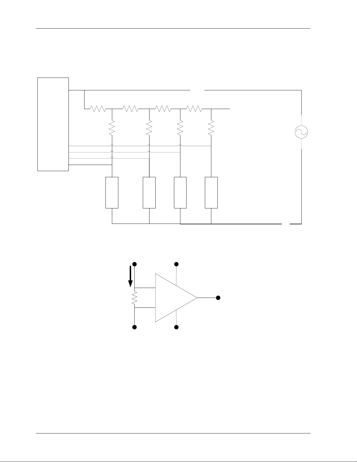
3 Circuit Description and Theory of Operation
Figure 3 shows a block diagram of the PDU1 Evaluation Board. For simplicity, only one of the 8 identical
channels is shown.
Figure 3: Differential PDU Block Diagram
The main functional blocks of the evaluation board are the 78M6618 energy measurement SoC, voltage
regulators, input signal conditioning, and relay control.
3.1 78M6618
The 78M6618 is a highly integrated IC for energy monitoring and measurement. The key features of the
78M6618 include:
• A 21-bit delta sigma analog to digital converter (ADC) with 10 multiplexed analog inputs
• A 32-bit digital signal processor core (Compute Engine, or CE)
• An 8-bit microprocessor core
• 128 Kbytes flash memory
• 32,768 kHz oscillator
• Up to 19 general-purpose digital I/O pins (DIO).
For detailed information on the 78M6618, refer to the 78M6618 Data Sheet.
3.2 Voltage Regulators
The evaluation board is powered by an external 12VDC source. The on-board relays for switching power
to the 8 outlets are powered directly from the 12V supply. Linear regulators are used to provide the 3.3V
supply for the 78M6618 and external logic and a 6.6V supply for the operational amplifiers that are used
to amplify the voltage from the current sense resistors.
Rev 3 13
Page 14

78M6618 PDU1 Evaluation Board User Manual UM_6618_022
3.3 Input Signal Conditioning
Input signal conditioning includes the voltage divider used to reduce the AC line voltage to a level that can
be measured by the 78M6618, the differential amplifiers that are used to remove common-mode voltage
from the input signals to the ADC current channels, and the low-pass filters that block high-frequency
signal content from the ADC inputs.
3.4 Relay Control
Power to each of the 12 outlets on the board is switched by a relay. The relays are individually controlled
by digital I/O (DIO) lines from the 78M6618. Do to the type of relay driver circuit used on this board, the
firmware Relay Config register (0x0210) is set equal to 2. This inverts the relay driver input polarity.
3.5 Theory of Operation
Before describing the operation of the PDU, it may be helpful to make note of some of the characteristics
of the 78M6618 and the board design.
1. The reference for the 78M6618’s ADC is its positive power supply (V3P3), not ground.
2. The 78M6618’s 3.3V power supply is directly connected to the neutral side of the AC power source.
As a result, the 78M6618’s ground reference is actually 3.3V below the AC neutral.
3.5.1 78M6618 Operation
The analog multiplexer at the front end of the delta-sigma ADC sequentially presents the signals at the 10
analog input pins to the ADC, which converts them to digital words which are presented to the 32-bit
compute engine (CE). The CE performs filtering and calculates RMS voltage and current, line frequency,
real power and reactive power. The CE transfers its results to the 80515 MPU at the end of each
accumulation interval. The accumulation interval, which is the period over which RMS voltage, current
and power are calculated, is determined by the firmware loaded into the 78M6618’s internal flash, and
may be between 200 milliseconds and 1 second. The 80515 MPU performs some scaling of the CE
results, calculates some additional values, and manages the communication with an external host via its
integrated UART. The MPU also controls the operation of the CE.
3.5.2 Voltage and Current Measurement
As previously described, the reference voltage for the 78M6618 ADC is 3.3V. The valid input range for
the ADC is 3.3V ±250 mV. A 250 mV signal corresponds to full scale on the ADC. A voltage divider is
used to scale the line voltage to the ±250 mV range of the ADC. The voltage divider consists of 2 1 MΩ
resistors and one 750 Ω resistor. The ADC measures the voltage across the 750Ω resistor, which is
0.0375% of the line voltage. With this ratio, the ADC can measure line voltages up to 667V
corresponds to a sinusoidal voltage input of ~471 V
limits the frequency content of the input signal to around 4,500 Hz.
The PDU uses current sense resistors, also known as shunt resistors, to sense the current flowing in the
neutral or return of each outlet. The value of the current sense resistor is selected to scale the voltage
drop across the resistor to the input range of the ADC. The sense resistors must also have low resistance
values in order to keep voltage drop and power dissipation to acceptable levels. The 78M6618’s ADC has
single ended inputs referenced to V3P3. The PCB traces that are used for the line and neutral buses on
the PDU board have resistances that are of the same magnitude or greater than that of the acceptable
shunts. This parasitic resistance appears between the reference end of the sense resistors and the ADCs
reference point, as illustrated by Figure 4. If the sense resistors are corrected directly to the ADC inputs
as shown in Figure 5, it is impossible to separate the voltage across the sense resistors from the voltage
across the parasitic resistance in the PCB. Because of this, current flowing in one outlet will affect the
voltage at the ADC current measurement inputs for other channels, resulting in channel-to-channel
crosstalk. To eliminate this problem, differential amplifiers are used between the current sense resistors
and the ADC current measurement inputs, as shown in Figure 5. The differential amplifier is biased to
provide an output centered at 3.3V, and rejects the voltage drop due to the PCB resistance, which
appears as common mode voltage at the amplifier inputs, so that the signal presented at the ADC input is
. An RC low-pass filter at the input to the ADC
RMS
PEAK
, which
14 Rev 3
Page 15
UM_6618_022 78M6618 PDU1 Evaluation Board User Manual
RshuntRshunt
Rshunt
Load
Load
Load
Load
78M6618
Runknown Runknown
Runknown Runknown
AC
Line
Neutral
Rshunt
ADC
Reference
Current
Sense
Inputs
Differential
Amplifier
-
+
Current
Sense
Resostor
AC Return
from load
AC Neutral
V6P6
GND
To LPF
and ADC
Input
Load Current
due only to the voltage drop across the current sense resistor. An additional advantage of using the
differential amplifier is that it is possible to use lower value sense resistors by increasing the gain of the
differential amplifier. The PDU evaluation board uses 500 µΩ sense resistors, with an amplifier gain of 10.
With this configuration, a peak current of 50A results in full-scale input to the ADC. This allows the PDU to
measure 16A loads with a crest factor slightly greater than 3.
Figure 4: PCB Parasitic Resistance
The layout of the feedback networks for the differential amplifiers is critical to provide true differential
Figure 5: Differential Amplifier and Current Sense Resistor
operation and to avoid noise pickup due to the high voltages and currents present on the PDU1 board.
Figure 6 shows a detail view of the current sense resistors, the dual op amp, and their feedback
networks.
Rev 3 15
Page 16
78M6618 PDU1 Evaluation Board User Manual UM_6618_022
Figure 6: Detail View of Differential Amplifiers
The op amps and their feedback networks are laid out to minimize the interconnect distance between the
current sense resistors and the op amp inputs. They are also located above a V3P3 plane to minimize
electrical noise pickup. For more detailed information on PCB layout, refer to the application note
Designing a Differential Power Distribution Unit Using the 78M6618.
16 Rev 3
Page 17
UM_6618_022 78M6618 PDU1 Evaluation Board User Manual
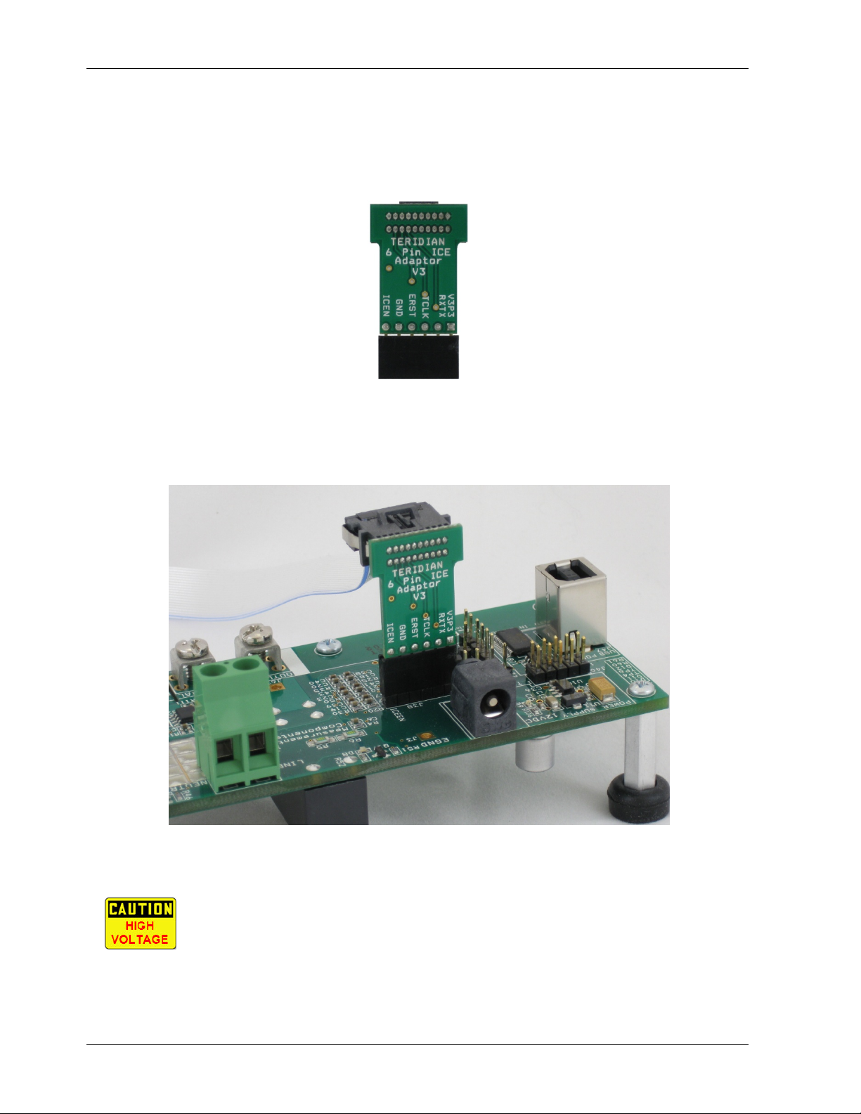
4 In-Circuit Emulator (ICE) Adaptor
The 78M6618’s firmware (stored in internal flash memory) can be updated to accommodate program
enhancements. Use the Signum ADM51 or the Teridian TFP2 to download new firmware to the 78M6618.
The supplied ICE Adaptor is required to interface the flat ribbon cable (provided with the ADM51 or TFP2)
to the 78M6618 evaluation board.
Figure 7: ICE Adaptor
Figure 3 shows how to attach the ICE Adaptor to the 78M6618 evaluation board. Please make note of the
orientation of the ICE Adaptor as to how it attaches to the 78M6618 evaluation board (V3P3 ICE Adaptor
pin connects to the +V Evaluation Board pin).
Figure 8: 78M6618 ICE Adaptor Attachment
Disconnect the 78M6618 evaluation board from live AC voltages before connecting the
ADM51 or TFP2. An Earth ground disparity and high AC voltages are present on the
78M6618 evaluation board when it is connected to the AC outlet. Equipment damage to
the 78M6618, ADM51/TFP2 and attached PC may occur when live AC voltages are
present on the 78M6618 evaluation board. Refer to the 78M661x Safety Precautions
Applications Note for additional information.
It is recommended to always use the supplied flat ribbon cable. Do not use discrete wires in place of the
flat ribbon. Poor signal integrity will cause flash memory programming errors. Additional adaptors and flat
ribbon cables can be ordered through Maxim.
Rev 3 17
Page 18
78M6618 PDU1 Evaluation Board User Manual UM_6618_022
x
XIN
LINEV
LINE 2,3
NEUTRAL 2,3
R6
1M 0.1%
1206W
R5
1M 0.1%
1206W
MS 660-RN732BTTD1004B25
+
C2
10uF 25V
DigiKey 478-1762-1-ND
1812
C6
1000pF
0603
XOU T
R9
1M 0.1%
1206W
U10
78L33
IN3OUT
1
GND
2
J48
5VEXT
RAPC712A
MS 502-RAPC712X
1
2
3
C8
1000pF
0603
U11
78L33
IN3OUT
1
GND
2
OUTCUR83
Title
Size Document Number Rev
Date: Sheet
of
Power Distribution U nit 8 Outlet Dif ferential C urrent Single Phase
TERIDIAN SEMICONDUCTOR CORP.
B
1 4Tuesday, May 10, 2011
C36
1uF
0603
D9
Red LED
.
R106
11K
LOGO2
1
TERIDIAN
LOGO1
1
Warning
R8
1M 0.1%
1206W
MS 660-RN732BTTD1004B25
MT1 MT2
C14
1uF
0603
GND
J3
CON1
1
Black
White
Green
GND
DigiKey 160-1181-6-ND
GND
GND
V3P3
C15
0.1uF
0603
C12
1uF 20V
1206P
3.3V below
Neutral
V3P3
connected t o
NEUTRAL
EGND
External wire to
J2 center point
12 VDC Input
+
C30
10uF 25V
DigiKey 478-1762-1-ND
1812
OUTCUR22
C7
33pF
0603
C9
9pF
0603
Y1
32.768KHz
CM200S
535-9166-1-ND
14
GND
OUTCUR32
V3P3
OUTCUR53
+12VDC
OUTCUR42
OUTCUR73
MT4MT3 MT5
OUTCUR63
MT6
3.3V above Neutral (V3P3)
V6P6
GND
Tyco 640454-2
GND
To Relays
V3P3
OUTCUR12
C1
0.1uF
0603
C4
NC
0603
+/-178mVrms
V3P3
V3P3
V1
R2
2K
0603
V2P5
EGNDV
VREF
C5
100pF
0603
+/-250mVpp
R3
20.0K 1%
0603
C3
0.1uF
0603
R1
16.9K 1%
0603
GND
LINE
U1-1
78M6618-68QFN
QFN68
V2P5
48
V3P3A
51
IA
61
IB
60
ID
58
IC
59
VREF
62
IF
56
IE
57
IG
55
V1
63
GNDA1
50
IH
54
VA
53
VB
52
XIN
66
XOU T
68
GNDA2
65
R4
750 0.1%
0603
+
C35
10uF 25V
DigiKey 478-1762-1-ND
1812
R7
750 0.1%
0603
J4
terminal block
1
2
NEUTRAL
A98275-ND
+
C13
220uF 25V lo imp
UUDB
MS 647-UUD1E221MNL
All things ref erenced to V3P3 f or 78M6618
Note: SMA GND shield is -3.3V relativ e to Neutral (Earth GND )
V3P3 connected t o NEUTRAL for Saf ety due to SMA GND shield
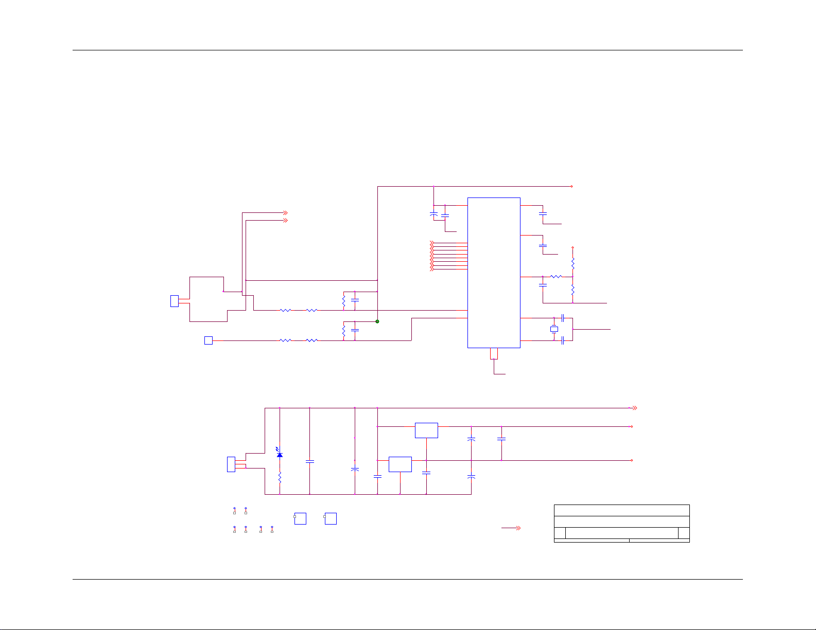
5 Schematics, Bill of Materials, and PCB Layouts
This section includes the schematics, bill of materials and PCB layouts for the 78M6618 PDU1 evaluation board.
5.1 78M6618 PDU1 Evaluation Board Schematics
18 Rev 3
Figure 9: 78M6618 PDU1 Evaluation Board Electrical Schematic (1 of 4)
Page 19
UM_6618_022 78M6618 PDU1 Evaluation Board User Manual
Egnd/Green
Neutral/White
Line/Black
NUD3112LT1GOSCT-ND
Neutral/White
Line/Black
Egnd/Green
R17
10K
0603
Neutral1/W hite
-
+
U4B
MAX4494/SO
7
5
6
8 4
R21
10K
0603
Neutral2/W hite
Neutral3/W hite
Neutral4/W hite
R73
75K
0603
-
+
U4A
MAX4494/SO
1
3
2
4 8
R74
7.5K
0603
GND
RLY2
R75
7.5K
0603
R76 75K
0603
Line/Black
Neutral/White
Egnd/Green
V6P6
GND
J50
CON1
1
J49
CON1
1
Q11
NUD3112/ SOT
C46
0.1UF
0603
NEUTRAL
J52
CON1
1
J51
CON1
1
J54
CON1
1
J53
CON1
1
GND
J55
CON1
1
J56
CON1
1
NEUTRAL1,3
V3P3
C47
0.1UF
0603
+12VDC
R83
7.5K
0603
R82
75K
0603
R85
75K
0603
R84
7.5K
0603
GND
GND
Q13
NUD3112/ SOT
C37
.047uF
0603
OUTCUR1
RELAY1 4
V6P6
RELAY2 4
GND
V3P3
C38
.047uF
0603
R26
10K
0603
Q12
NUD3112/ SOT
+12VDC
GND
D1
LED
OUTCUR2
J7
CON4
STERM
MS 534-8191
1
2
3
4
R78
7.5K
0603
R77
75K
0603
R79
7.5K
0603
R80 75K
0603
Q10
NUD3112/ SOT
R81
.0005
2512P
MS 66-ULR25R006FLF TR
Title
Size Doc ument Number Rev
Date: Sheet
of
Power Distribution U nit 8 Outlet Dif ferent ial Current Single Phase
TERIDIAN SEMICONDUCTOR CORP.
B
2 4Tuesday, May 10, 2011
C39
.047uF
0603
J8
CON4
STERM
MS 534-8191
1
2
3
4
LINE
NEUTRAL
OUTL ET3
OUTL ET2
OUTL ET1
OUTL ET4
RLY4
RLY3
R19
.0005
2512P
MS 66-ULR25R006FLF TR
D2
LED
C18
1000pF
0603
C19
1000pF
0603
RL4
16A 12V SPDT Low Profile
ALZ
255-1446-ND
3
5
4
1
2
6
7
8
RL1
16A 12V SPDT Low Profile
ALZ
255-1446-ND
3
5
4
1
2
6
7
8
J9
CON4
STERM
MS 534-8191
1
2
3
4
RL2
16A 12V SPDT Low Profile
ALZ
255-1446-ND
3
54
1
2
6
7
8
R27
2K
0603
R30
750
0603
RL3
16A 12V SPDT Low Profile
ALZ
255-1446-ND
3
54
1
2
6
7
8
R22
2K
0603
C20
1000pF
0603
R32
2K
0603
R35
750
0603
R29
.0005
2512P
MS 66-ULR25R006FLF TR
R20
750
0603
J10
CON4
STERM
MS 534-8191
1
2
3
4
R34
.0005
2512P
MS 66-ULR25R006FLF TR
R25
750
0603
R16
2K
0603
C17
1000pF
0603
D3
LED
V3P3
V3P3
LINE1,3
OUTCUR3 1
OUTCUR2 1
OUTCUR1 1
OUTCUR3
OUTCUR4 1
.
RELAY3 4
LED, Green
LED, Green
-
+
U5A
MAX4494/SO
1
3
2
4 8
J11
CON4
STERM
MS 534-8191
1
2
3
4
C45
0.1UF
0603
C48
0.1UF
0603
V3P3
J12
CON4
STERM
MS 534-8191
1
2
3
4
D4
LED
C40
.047uF
0603
J13
CON4
STERM
MS 534-8191
1
2
3
4
-
+
U5B
MAX4494/SO
7
5
6
8 4
J14
CON4
STERM
MS 534-8191
1
2
3
4
+12VDC1,3
OUTCUR4
V6P6
GND
+12VDC
R31
10K
0603
+12VDC
GND
V3P3
RELAY4
4
V6P6
R86
75K
0603
R88
7.5K
0603
R87
7.5K
0603
R89
75K
0603
Egnd/Green
Neutral/White
Line/Black
DigiKey 475-1409-1-ND
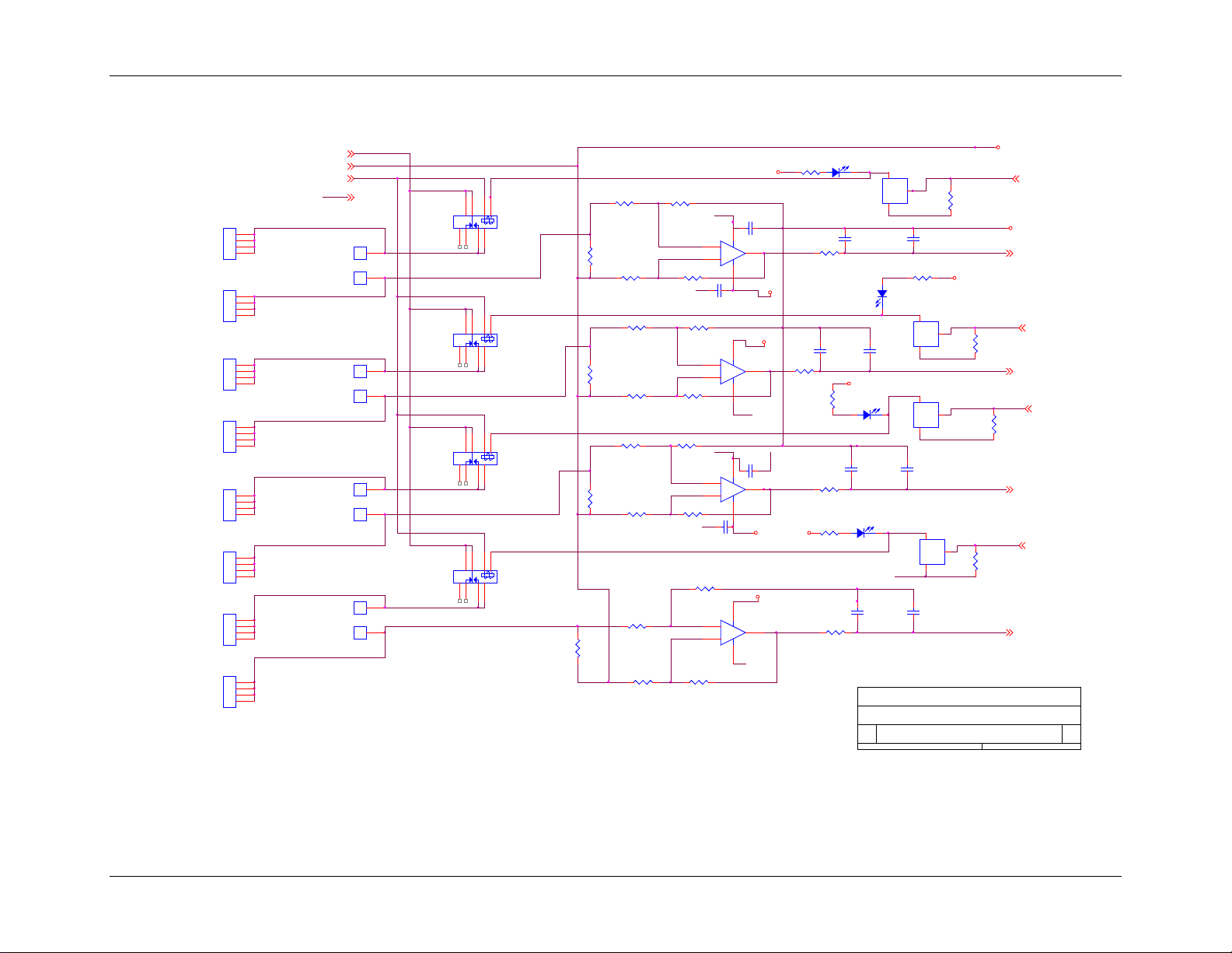
Rev 3 19
Figure 10: 78M6618 PDU1 Evaluation Board Electrical Schematic (2 of 4)
Page 20
78M6618 PDU1 Evaluation Board User Manual UM_6618_022
-
+
U7A
MAX4494/SO
1
3
2
4 8
C52
0.1UF0603
R42
2K
0603
R102
75K
0603
R104
7.5K
0603
R103
7.5K
0603
R105
75K
0603
-
+
U7BMAX4494/SO
7
5
6
8 4
GND
R47
2K
0603
GND
Q15
NUD3112/ SOT
R52
2K
0603
RLY6
RELAY6 4
NEUTRAL
V6P6
GND
RLY7
Q16
NUD3112/ SOT
RLY8
R108NC
GND
Neutral/White
Line/Black
Neutral1/ White
Egnd/Green
Egnd/Green
Neutral/White
Line/Black
Neutral1/ White
Egnd/Green
Neutral/White
Line/Black
Neutral1/ White
R109NC
GND
Egnd/Green
Neutral/White
Line/Black
Neutral1/ White
V6P6
R36
10K
0603
RELAY7 4
R110NC
R46
10K
0603
Title
Size Document N umber Rev
Date: Sheet
of
Power Distribut ion Unit 8 Outlet Dif ferent ial Current Single Phase
TERIDIAN SEMICONDUCTOR CORP.
B
3 4Wednesday , May 11, 2011
NEUTRAL1,2
LINE
NEUTRAL
OUTL ET5
RELAY8 4
OUTL ET8
OUTL ET7
OUTL ET6
GND
R39
2512P
MS 66-ULR25R006F LFTR
R54
.0005
2512P
MS 66-ULR25R006F LFTR
C22
1000pF
0603
R55
750
0603
RL5
16A 12V SPDT Low Profile
ALZ
255-1446-ND
3
54
1
2
6
7
8
R45
750
0603
RL8
16A 12V SPDT Low Profile
ALZ
255-1446-ND
3
54
1
2
6
7
8
RL6
16A 12V SPDT Low Profile
ALZ
255-1446-ND
3
54
1
2
6
7
8
C24
1000pF
0603
C21
1000pF
0603
R40
750
0603
R49
.0005
2512P
MS 66-ULR25R006F LFTR
R50
750
0603
GND
R37
2K
0603
R44
.0005
2512P
MS 66-ULR25R006F LFTR
C23
1000pF
0603
RL7
16A 12V SPDT Low Profile
ALZ
255-1446-ND
3
5412
6
7
8
V3P3
LINE1,2
OUTCUR6 1
OUTCUR5 1
NUD3112LT1GOSCT-ND
OUTCUR8 1
OUTCUR7 1
.
DigiKey 475-1409-1-ND
LED, Green
LED, Green
J58
CON1
1
R98
7.5K
R100
7.5K
0603
R99
75K
R101
75K
0603
V6P6
V6P6
R91
7.5K
0603
R90
75K
0603
R92
7.5K
0603
J60
CON1
1
J59
CON1
1
J62
CON1
1
J61
CON1
1
J64
CON1
1
J63
CON1
1
NEUTRAL
C41
.047uF
0603
GND1,3
RELAY5 4
V3P3
OUTCUR5
J57
CON1
1
V6P6
Q17
NUD3112/ SOT
C49
0.1UF
0603
V3P3
C42
.047uF
0603
J15
CON4
STERM
MS 534-8191
1
2
3
4
C43
.047uF
0603
J16
CON4
STERM
MS 534-8191
1
2
3
4
C44
.047uF
0603
J17
CON4
STERM
MS 534-8191
1
2
3
4
C50
0.1UF
0603
R41
10K
0603
V3P3
J18
CON4
STERM
MS 534-8191
1
2
3
4
GND
OUTCUR6
J19
CON4
STERM
MS 534-8191
1
2
3
4
R94
7.5K
0603
R96
7.5K
0603
R95
75K
0603
R97
75K
0603
J20
CON4
STERM
MS 534-8191
1
2
3
4
C51
0.1UF0603
R107NC
J21
CON4
STERM
MS 534-8191
1
2
3
4
Q14
NUD3112/ SOT
R51
10K
0603
R93
75K
0603
R111NC
R113NC
R112NC
R114NC
J22
CON4
STERM
MS 534-8191
1
2
3
4
NEUTRAL
GND
OUTCUR7
D5
LED
-
+
U6AMAX4494/SO
1
3
2
4 8
NEUTRAL
D6
LED
D7
LED
OUTCUR8
-
+
U6B
MAX4494/SO
7
5
6
8 4
D8
LED
RLY5
+12VDC1, 3
Figure 11: 78M6618 PDU1 Evaluation Board Electrical Schematic (3 of 4)
20 Rev 3
Page 21
Title
Size Document N umber Rev
Date: Sheet
of
Power Distribut ion Unit 8 Outlet Dif ferent ial Current Single Phase
TERIDIAN SEMICONDUCTOR CORP.
B
4 4Tuesday , May 10, 2011
R61
10K
0603
TP3
SIP100P2
Wh
1
2
DigiKey 475-1409-1-ND
Pulse Output
V3P3
TP6
TP
TPWW
1
.
PCLK
GND
MISO
PWRUP
TRXCE
CSN
no connect
TXEN
MOSI
CD
DR
SCKDIO4
DIO5
DIO43
DIO19
DIO16
DIO17
DIO18
DIO1
DIO2
DIO3
no connect
no connect
PacketPowerOneNetSM BusJ37
Pins
SMBALTRB
SMBTXLOB
SMBCLOCK
SMBRXD
no connect
SLE
CE
no connect
no connect
SMBCKHDB DATAIO
DATACLK
INT
SCLK
SREAD
SDATA
GND
GND
PSDI
D10
READY
TP1
TP
TPWW
1
V3P3
TP7
TP
TPWW
1
DIO3
PSDO
D11
LED
TP2
TP
TPWW
1
GND
GND
PCSZ
RELAY3 2
C27
1uF
810-C1608X5R1C105M
0603
C25
0.1uF
0603
UTX
GND
J40
SPI1
DIP100P10
1 2
3 4
5 6
7
8
9 10
RELAY5 3
R62
470
0603
R15
470
0603
V3P3
RELAY2 2
D12
Red LED
DIO17
RELAY7 3
DIO18
V3P3
RELAY4 2
GND
GND
V3P3
RELAY6 3
C26
0.1uF
0603
LED, GrnLED, Y el
GNDGND
DIO6
U2
28-LD SSOP
28-SSOP
768-1007-1-ND
VCC
20
USBDM
16
USBDP
15
VCCIO
4
NC1
8
RESETB
19
OSCI
27
RXD
5
RTS
3
CTS
11
DTR
2
DSR
9
RI
6
CBUS0
23
TXD
1
OSCO
28
CBUS1
22
CBUS2
13
CBUS3
14
CBUS4
12
3V3OUT
17
AGND25GND1
7
GND218GND3
21
TEST
26
NC2
24
DCD
10
DIO16
GNDGND
GND
DIO19
J66
CON2
1
2
DIO43
NEUTRAL1,2
DIO4
DigiKey 160-1181-6-ND
URX
R58
330
0603
C29
1000pF
0603
TCLK
RXT X
J47
USB-B
USBBV
MS 806-KUSBVX-BSIN-W
1
2
3
4
5
6
ACTIVE
ICE inputs become
ERST
when ICEE low
LCD seg driv ers
V3P3
J38
ICE
SIP100P6
1
2
3
4
5
6
ICEEN
USBDM
USB5V
V3P3
USBRX
can source upto 50ma
U2 internal 3. 3V LDO
USBDP
USBTX
U3
ADUM3201
ADUM3201
ADUM3201ARZ-ND
VOA
2
V1
1
ND1
4
V2
8
VIA
7
G2
5
VIB3VOB
6
USB3V
C31
4.7uF
1206P
USBGND
C32
0.1uF
0603
Mouser 571-1487588-2
1.5M A/B Whit e Cable
ADI TX/RX data interf ace
DIO1
DIO2
GND
DIO5
PCLK
SCL
PSDI
SDA
J67
CON2
1
2
SDI
CLK
PSDO
Must use iso lated USB hub
CSZ
SDO
PCSZ
CSZ
SDO
SDI
CLK
LED, Red
R60
470
0603
V3P3
C28
R57
R56
SW1
Optional Res et Switch
1000pF
1K
1K
EVQ-PJX05M Panasonic
J39
DEBUG
SIP100P4
1
2
3
4
TP4
TEST POINT
1
R59
10K
0603
R71
0
0603
C33
0.1uF
0603
RELAY1 2
RELAY8 3
TP5
TP
TPWW
1
DigiKey 160-1184-1-ND
I2C Master
for
EEPROM
Internal s lave SPI cont roller
U1-2
78M6618-68QFN
QFN68
SEG12
30
SEG2
21
SEG17
34
SEG16
33
RESET
49
SEG18
35
V3P3D
9
ERXTX/SEG9
4
SDCK/D IO4/SEG24
37
SDATA/DIO5/ SEG25
38
ERST/SEG11
1
ETCLK/SEG10
2
DIO13/SEG33
29
SEG15
32
RX
46
SEG1
20
SEG7
26
SEG8
27
TX
7
SEG0
19
VBAT
47
COM1
18
COM0
17
CKTEST/SEG19
10
DIO17/SEG37
14
PSDI/SEG6
25
DIO18/SEG38
15
TEST
67
SEG14
31
PCSZ/SEG5
13
PSDO/SEG4
12
PCLK/SEG3
8
GNDD1
3
ICEE
36
V3P3SYS
11
WPULSE/D IO6/SEG26
39
DIO8/SEG28
42
DIO9/SEG29
43
DIO10/SEG30
44
DIO11/SEG31
45
DIO43/SEG63
28
DIO14/SEG34
22
DIO15/SEG35
23
DIO16/SEG36
24
TMUXOU T
6
DIO7/SEG27
40
OPTX/DIO2
5
OPRX/DIO1
64
DIO3
16
DIO19/SEG39
41
SM Bus Address
Alternate
bit-bang SPI
interf ace
R72
0
0603
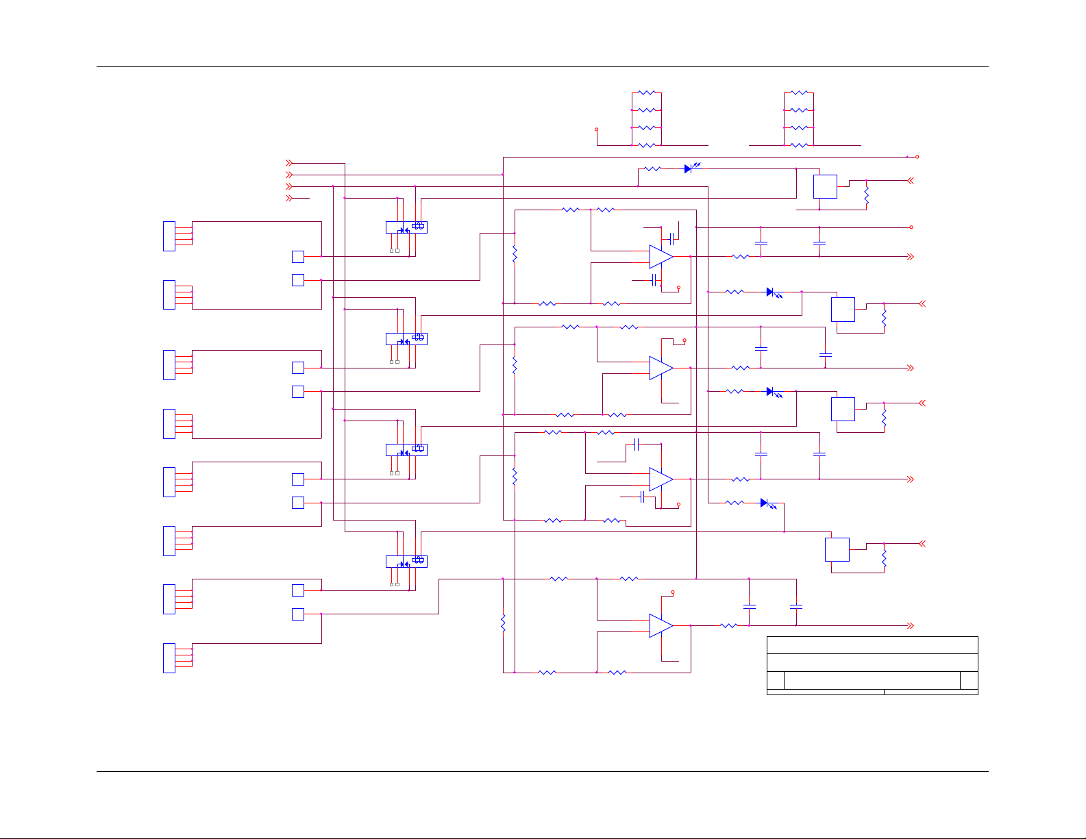
UM_6618_022 78M6618 PDU1 Evaluation Board User Manual
Figure 12: 78M6618 PDU1 Evaluation Board Electrical Schematic (4 of 4)
Rev 3 21
Page 22

78M6618 PDU1 Evaluation Board User Manual UM_6618_022
MS - Mouser
C1,C3,C15,C25,C26,C32,C33,
2 3 C2,C30,C35
10µF 25V
2312
399-3734-1-ND
T491C106K025AT
KEMET
Yes
3 1 C4
0603
DNP
—
—
—
4 1 C5
100pF
0603
445-1281-1-ND
C1608C0G1H101J
TDK Corporation
Yes
Yes
Yes
6 1 C7
33pF
0603
399-1055-1-ND
C0603C330J5GACTU
KEMET
Yes
7 1 C9
9pF
0603
445-5046-1-ND
C1608C0G1H090C
TDK Corporation
Yes
CC1206KKX7R8BB10
5
220µF 25V lo
imp
GRM188R61E105KA1
2D
11 1 C31
4.7µF
1206
399-4630-1-ND (1206)
T491A475M025AT
KEMET
Yes
C37,C38,C39,C40,C41,C42,
C43,C44
GRM188F51H473ZA0
1D
OSRAM Opto
Semiconductors
15 1 D10
Yellow LED
0603
160-1184-1-ND
LTST-C190YKT
Lite-On Inc.
Yes
J3,J49,J50,J51,J52,J53,J54,
J62,J63,J64
17 1 J4
TERM BLOCK
Through Hole
A98275-ND
796740-2
TE Connectivity
Yes
J7,J8,J9,J10,J11,J12,J13,J14,
Sullins Connector
Solutions
Sullins Connector
Solutions
5.2 78M6618 PDU1 Evaluation Board Bill of Materials
Table 2: 78M6618 PDU1 Evaluation Board Bill of Materials
Item Qty Reference Part
1 15
5 11
8 1 C12
9 1 C13
10 3 C14,C27,C36
12 8
13 9 D1,D2,D3,D4,D5,D6,D7,D8,D11 Green LED 0603 475-1409-1-ND LG Q971-KN-1
C45,C46,C47,C48,C49,C50,
C51,C52
C6,C8,C17,C18,C19,C20,C21,
C22,C23,C24,C29
0.1µF 0603 399-5089-1-ND C0603C104K5RACTU KEMET Yes
1000pF 0603 445-1298-1-ND C1608X7R2A102K TDK Corporation
1µF 25V
1µF (0603)
.047µF
PCB
Footprint
1206 311-1356-1-ND
SMD 493-2278-1-ND UUD1E221MNL1GS Nichicon Yes
0603 490-3897-1-ND
0603 490-1567-1-ND
Digi-Key
Part Number Manufacturer RoHS
Yageo Yes
Murata Yes
Murata Yes
Yes
14 2 D9,D12 Red LED 0603 160-1181-6-ND LTST-C190CKT Lite-On Inc. Yes
16 17
18 16
19 1 J38 ICE Through Hole S1011E-36-ND PBC36SAAN
20 1 J39 DEBUG Through Hole S1011E-36-ND PBC36SAAN
J55,J56,J57,J58,J59,J60,J61,
J15,J16,J17,J18,J19,J20,J21,
J22
22 Rev 3
CON1 Through Hole DNP — — —
CON4 Through Hole MS 534-8191 8191
Keystone
Electronics
Yes
Yes
Yes
Page 23

UM_6618_022 78M6618 PDU1 Evaluation Board User Manual
Digi-Key
Sullins Connector
Solutions
MS 806-KUSBVX-
BS1N-B
23 1 J48
RAPC712A
Through Hole
MS 502-RAPC712X
RAPC712X
Switchcraft
Yes
Sullins Connector
Solutions
Sullins Connector
Solutions
INDCT
DRVR
RL1,RL2,RL3,RL4,RL5,RL6,RL
16A 12V SPDT
29 1 R1
16.9K 1%
0603
P16.9KHCT-ND
ERJ-3EKF1692V
Panasonic
Yes
R2,R16,R22,R27,R32,R37,R42,
R47,R52
31 1 R3
20.0K 1%
0603
P20.0KHCT-ND
ERJ-3EKF2002V
Panasonic
Yes
32 2 R4,R7
750 0.1%
0603
P750YCT-ND
ERA-3YEB751V
Panasonic
Yes
MS 660-
RN732BTTD1004B25
34 3 R15,R60,R62
470
0603
P470GCT-ND
ERJ-3GEYJ471V
Panasonic
Yes
R17,R21,R26,R31,R36,R41,R4
6,R51,R59,R61
R19,R29,R34,R39,R44,R49,R5
MS 66-
ULRB22512R0005FL
R20,R25,R30,R35,R40,R45,R5
38 1 R58
330
0603
P330HCT-ND
ERJ-3EKF3300V
Panasonic
Yes
39 2 R71,R72 0 0603
P0.0GCT-ND
ERJ-3GEY0R00V
Panasonic
Yes
Item Qty Reference Part
21 1 J40 SPI1 Through Hole S2011E-36-ND PBC36DAAN
22 1 J47 USB-B Through Hole
24 2 J66,J67 CON2 Through Hole S1011E-36-ND PBC36SAAN
25 2 LOGO1,LOGO2 Logo Silkscreen — — — —
26 5 TP1,TP2,TP5,TP6,TP7 TP Through Hole S1011E-36-ND PBC36SAAN
27 8
28 8
30 9
33 4 R5,R6,R8,R9 1M 0.1% 1206
Q10,Q11,Q12,Q13,Q14,Q15,Q
16,Q17
7,RL8
LOAD/RELAY
Low Profile
2K 0603 P2.0KGCT-ND ERJ-3GEYJ202V Panasonic Yes
PCB
Footprint
SOT-23-3
Through Hole 255-1446-ND ALZ12F12 Panasonic Yes
MS - Mouser
NUD3112LT1GOSCT-
ND
Part Number Manufacturer RoHS
806-KUSBVX-BS1N-B Kycon Yes
NUD3112LT1G ON Semiconductor Yes
RN732BTTD1004B25 KOA Speer Yes
Yes
Yes
Yes
35 10
36 8
37 8
40 16
4,R81
0,R55
R73,R76,R77,R80,R82,R85,
R86,R89,R90,R93,R95,R97,
R99,R101,R102,R105
Rev 3 23
10K 0603 P10.0KHCT-ND ERJ-3EKF1002V Panasonic Yes
0.0005 2512
750 0603 P750GCT-ND ERJ-3GEY0R00V Panasonic Yes
75K 0603 RG16P75.0KBCT-ND RG1608P-753-B-T5 Susumu Yes
ULRB2R0005FLFSLT
FSLT
IRC Yes
Page 24

78M6618 PDU1 Evaluation Board User Manual UM_6618_022
Digi-Key
42 1 R106
11K
0603
P11KGCT-ND
ERJ-3GEYJ113V
Panasonic
Yes
R107,R108,R109,R110,R111,
Sullins Connector
Solutions
Sullins Connector
Solutions
46 1 U1
78M6618-68QFN
68-QFN — —
Maxim
Yes
47 1 U2
FTDI 28-SSOP
28-SSOP
768-1007-1-ND
FT232RL-REEL
FTDI
Yes
48 1 U3
ADUM3201
8-SOIC
ADUM3201ARZ-ND
ADUM3201ARZ
Analog Devices
Yes
ROHM
Semiconductor
50 2 U10,U11
78L33
SOT-89-3
497-1200-1-ND
L78L33ACUTR
STMicroelectronics
Yes
Abracon
Corporation
Keystone
Keystone
Electronics
B&F Fastener
Supply
Item Qty Reference Part
R74,R75,R78,R79,R83,R84,
41 16
43 8
44 1 TP3 Wh Through Hole S1011E-36-ND PBC36SAAN
45 1 TP4 TEST POINT Through Hole S1011E-36-ND PBC36SAAN
49 4 U4,U5,U6,U7 OP AMP 8-SOIC LM2904MXCT-nd LM2904MX
51 1 Y1 32.768KHz 4-SOJ 535-9166-1-ND ABS25-32.768KHZ-T
52 6 MT1,MT2,MT3,MT4,MT5,MT6 STANDOFFS Through Hole MS 534-1809 1809
53 6 standoff bumpers RUBBER N/A MS 534-720 720
R87,R88,R91,R92,R94,R96,
R98,R100,R103,R104
R112,R113,R114
7.5k 0603 RG16P7.5KBCT-ND RG1608P-752-B-T5 Susumu Yes
2.5k 0603 DNP — — —
PCB
Footprint
MS - Mouser
Part Number Manufacturer RoHS
Electronics
Yes
Yes
Yes
Yes
Yes
Yes
54 12 # 4 screws for stand offs Screws Through Hole H346 PMS 440 0050 PH
24 Rev 3
Yes
Page 25
UM_6612_016 78M6618 PDU1 Evaluation Board User Manual
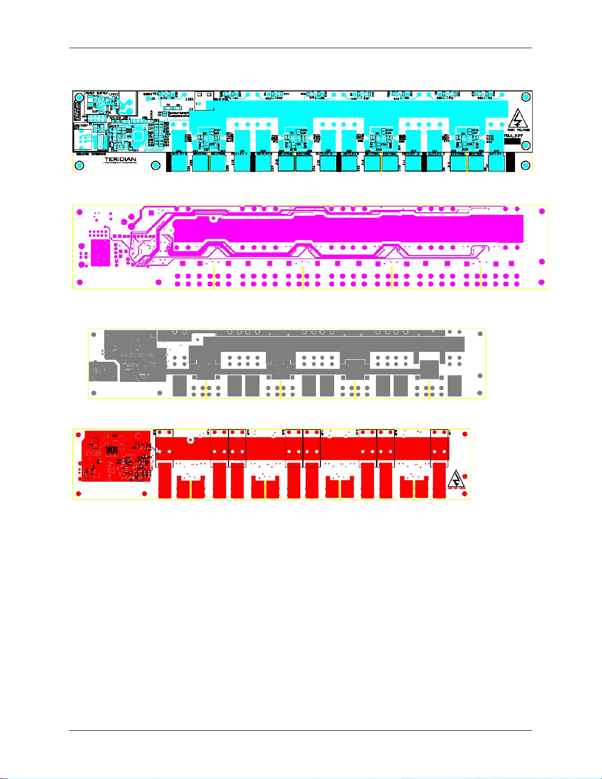
5.3 78M6618 PDU1 Evaluation Board PCB Layouts
Figure 13: 78M6618 PDU1 Evaluation Board PCB Top View
Figure 14: 78M6618 PDU1 Evaluation Board PCB Power View
Figure 15: 78M6618 PDU1 Evaluation Board PCB GND View
Figure 16: 78M6618 PDU1 Evaluation Board PCB Bottom View
Rev 3 25
Page 26

78M6618 PDU1 Evaluation Board User Manual UM_6618_022
Part Description
Order Number
6 Ordering Information
78M6618 PDU1 Evaluation Board 78M6618-PDU-1
7 Contact Information
For more information about Maxim products or to check the availability of the 78M6618, contact technical
support at
www.maxim-ic.com/support.
26 Rev 3
Page 27
UM_6618_022 78M6618 PDU1 Evaluation Board User Manual
Appendix A - 78M6618 PDU1 Board with CTs
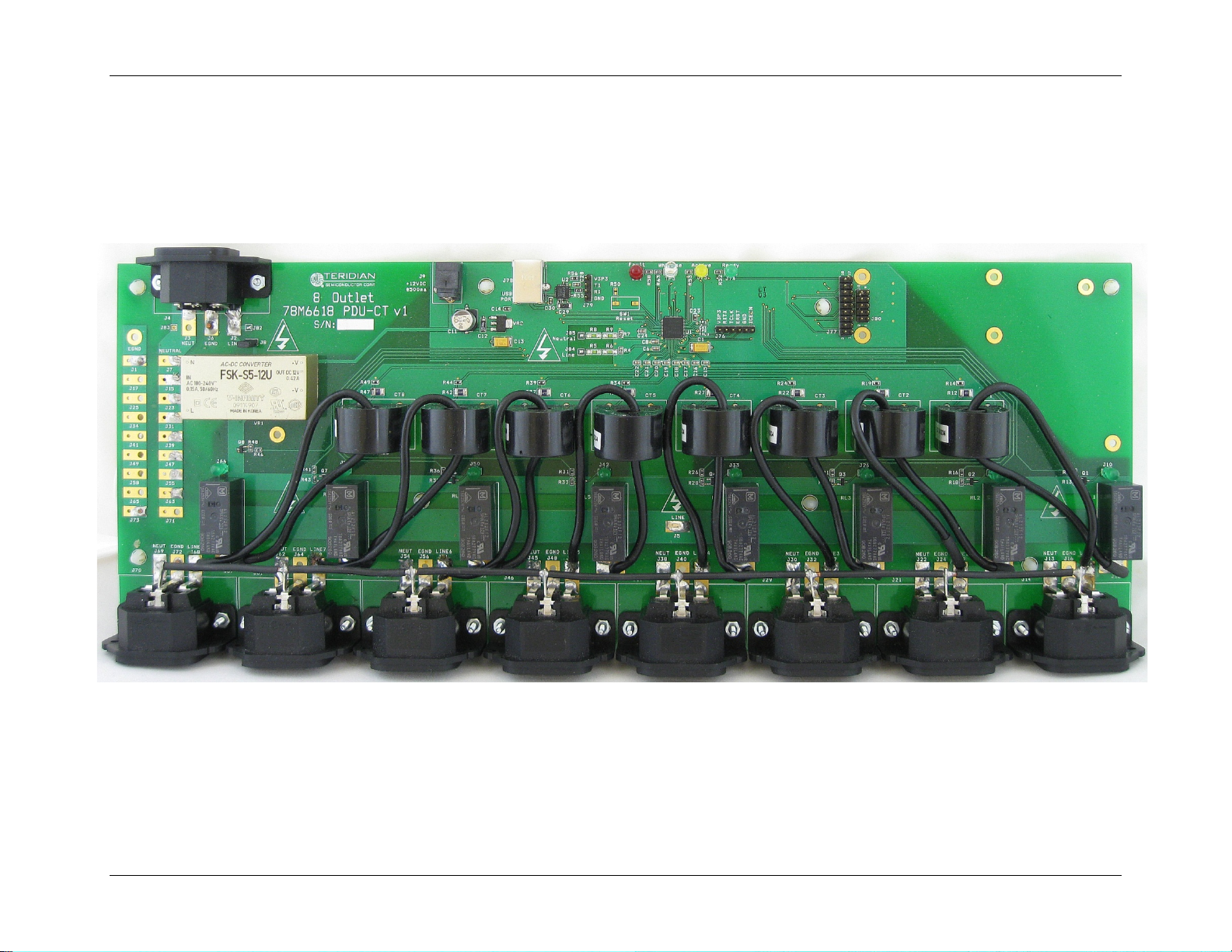
This appendix includes the photograph, schematics, bill of materials, and layout images for a comparable 78M6618 PDU1 evaluation board using
current transformers (CTs) in place of current shunt resistors. The information on this board is provided as reference only and is not available for
purchase.
A.1 78M6618 PDU-CT Evaluation Board
Figure 17: 78M6618 PDU-CT Evaluation Board
Rev 3 27
Page 28

78M6618 PDU1 Evaluation Board User Manual UM_6618_022
OUTCUR2
XIN
LINEV
LINE
OUTCUR3
NEUTRAL
R6
1M 0.1%
1206W
R5
1M 0.1%
1206W
MS 660-RN732BTTD1004B25
OUTCUR4
+
C1
10uF 25V
DigiKey 478-1762-1-ND
1812
C6
1000pF
0603
XOU T
R9
1M 0.1%
1206W
OUTCUR5
C8
1000pF
0603
OUTCUR6
OUTCUR7
OUTCUR8
MT3
MS 561-PS500A
Title
Size Document Number Rev
Date: Sheet
of
PDUCTV1 1
Power Distribution U nit 8 Outlet Single Phase with C Ts
TERIDIAN SEMICONDUCTOR CORP.
B
1 4Monday, March 01, 2010
GND
MT5
MS 561-PS500A
EGND
MT11
MS 561-PS500A
MT4
MS 561-PS500A
MT12
MS 561-PS500A
MT6
MS 561-PS500A
MT2
MS 561-PS500A
GND
.
LOGO2
1
TERIDIAN
J8
SIP100P2
Weco Tst
1
2
LOGO1
1
Warning
R8
1M 0.1%
1206W
MS 660-RN732BTTD1004B25
MT7
MT10
MT9MT8
LOGO6
1
Neutral/White
Line/Black
Egnd/Green
Black
White
Green
V3P3
+12VDC
C10
0.1uF
0603
J82
CON1
SIP100P1
1
EGND
C12
1uF 20V
1206P
C14
1uF
0603
LOGO3
1
J5
ACTERM
K1287
MS 534-1287-ST
1
2
LOGO4
1
LOGO5
1
+
C13
10uF 25V
DigiKey 478-1762-1-ND
1812
J9
Weco Tst
RAPC712A
MS 502-RAPC712
1
2
3
VR1
FSKS5-12V
FSKS5
102-1471-ND
GND
4
AC1
1
AC2
2
+12V
5
GND
C7
33pF
0603
C9
9pF
0603
Y1
32.768KHz
CM200S
535-9166-1-ND
1
4
J4
AC Inlet
PX0580
MS 562-PX0580/PC
1
2
3 VR2
+3.3V 500mA
MS 511-LD1117S33C
SOT223
VOUT
2
VIN
3
TAB
4
GND
1
V3P3
J2
CON1
SIPW2
1
MT13
MT16MT14
MT15
J1
ACTERM
K1287
MS 534-1287-ST
1
2
J3
CON1
SIPW2
1
GND
V3P3
LINE
To Relays
V3P3
OUTCUR1
C2
0.1uF
0603
C4
NC
0603
+/-178mVrms
V3P3
J6
CON1
SIPW2
1
V1
R2
2K
0603
GND
GND
V2P5
GND
NEUTV
GND
VREF
GND
C5
100pF
0603
+/-250mVpp
R3
20.0K 1%
0603
C3
0.1uF
0603
R1
16.9K 1%
0603
GND
U1-1
78M6618-68QFN
QFN68
V2P5
48
V3P3A
51
IA
61
IB
60
ID
58
IC
59
VREF
62
IF
56
IE
57
IG
55
V1
63
GNDA1
50
IH
54
VA
53
VB
52
XIN
66
XOU T
68
GNDA2
65
R4
750 0.1%
0603
J83
CON1
SIP100P1
1
J7
ACTERM
K1287
MS 534-1287-ST
1
2
R7
750 0.1%
0603
J84
CON1
SIP100P1
1
J85
CON1
SIP100P1
1
NEUTRAL
+
C11
220uF 25V lo imp
UUDB
MS 647-UUD1E221MNL
MT1
MS 561-PS500A
A.2 78M6618 PDU-CT Evaluation Board Schematics
Figure 18: 78M6618 PDU-CT Evaluation Board Electrical Schematic (1 of 4)
28 Rev 3
Page 29

UM_6618_022 78M6618 PDU1 Evaluation Board User Manual
R15
2K
0603
J18
SIP100P2
LED
1
2
Q1
NPN 500m a 30V
SOT23T
MS 512 -MMBTA13
GND
R20
2K
0603
J26
SIP100P2
LED
1
2
V3P3
J33
SIP100P2
LED
1
2
R25
2K
0603
RLY2
RELAY2
RLY3
RLY4
Neutral/White
Line/Black
Egnd/Green
Egnd/Green
Neutral/White
Line/Black
Q2
NPN 500m a 30V
SOT23T
MS 512 -MMBTA13
GND
R16
1K
0603
R18
10K
0603
Egnd/Green
Neutral/White
Line/Black
Egnd/Green
Neutral/White
Line/Black
RELAY3
Q3
NPN 500m a 30V
SOT23T
MS 512 -MMBTA13
GND
R23
10K
0603
R21
1K
0603
R17
4.99 1%
1210
MS 660-SR732ETTE4R99F
V3P3
CT2
CT020P2A
CT020P2A
Oswell
Title
Size Document N umber Rev
Date: Sheet
of
PDUCTV1
1
Power Distribut ion Unit 8 Outlet Single Phase with C Ts
TERIDIAN SEMICONDUCTOR CORP.
B
2 4Monday, March 01, 2010
OUTCUR4
NEUTRAL
+12VDC
+12VDC
+12VDC
+12VDC
LINE
NEUTRAL
OUTL ET1
RELAY4
OUTL ET4
OUTL ET3
OUTL ET2
EGND
Q4
NPN 500m a 30V
SOT23T
MS 512 -MMBTA13
GND
R26
1K
0603
R28
10K
0603
C16
1000pF
0603
R29
750
0603
RL1
16A 12V SPDT Low Profile
ALZ
255-1446-ND
3
5412
6
7
8
R19
750
0603
RL4
16A 12V SPDT Low Profile
ALZ
255-1446-ND
3
54
1
2
6
7
8
RL2
16A 12V SPDT Low Profile
ALZ
255-1446-ND
3
5412
6
7
8
V3P3
R22
4.99 1%
1210
MS 660-SR732ETTE4R99F
C18
1000pF
0603
C15
1000pF
0603
R14
750
0603
CT3
CT020P2A
CT020P2A
Oswell
R24
750
0603
R10
2K
0603
J10
SIP100P2
LED
1
2
C17
1000pF
0603
RL3
16A 12V SPDT Low Profile
ALZ
255-1446-ND
3
54
126
7
8
V3P3
LINE
+12VDC
OUTCUR2
OUTCUR1
OUTCUR4
OUTCUR3
.
EGND
MS 604-WP1503GD
LED, Green
V3P3
R27
4.99 1%
1210
MS 660-SR732ETTE4R99F
MS 604-WP1503GD
LED, Green
CT4
CT020P2A
CT020P2A
Oswell
OUTCUR2
OUTCUR3
OUTCUR1
J21
AC Outlet
PX0675
MS 562-PX0675/PC
1
2
3
J22
CON1
SIPW2
1
J19
CON1
SIPW2
1
J24
CON1
SIPW2
1
J29
AC Outlet
PX0675
MS 562-PX0675/PC
1
2
3
J30
CON1
SIPW2
1
J27
CON1
SIPW2
1
J32
CON1
SIPW2
1
J37
AC Outlet
PX0675
MS 562-PX0675/PC
1
2
3
J38
CON1
SIPW2
1
J36
CON1
SIPW2
1
J40
CON1
SIPW2
1
J11
CON1
SIPW2
1
J13
CON1
SIPW2
1
J14
AC Outlet
PX0675
MS 562-PX0675/PC
1
2
3
J16
CON1
SIPW2
1
J12
ACTERM
K1287
MS 534-1287-ST
1
2
J17
ACTERM
K1287
MS 534-1287-ST
1
2
J15
ACTERM
K1287
MS 534-1287-ST
1
2
J23
ACTERM
K1287
MS 534-1287-ST
1
2
J20
ACTERM
K1287
MS 534-1287-ST
1
2
J25
ACTERM
K1287
MS 534-1287-ST
1
2
J31
ACTERM
K1287
MS 534-1287-ST
1
2
J28
ACTERM
K1287
MS 534-1287-ST
1
2
J34
ACTERM
K1287
MS 534-1287-ST
1
2
R13
10K
0603
R11
1K
0603
RELAY1
J35
ACTERM
K1287
MS 534-1287-ST
1
2
J39
ACTERM
K1287
MS 534-1287-ST
1
2
J41
ACTERM
K1287
MS 534-1287-ST
1
2
R12
4.99 1%
1210
MS 660-SR732ETTE4R99F
CT1
CT020P2A
CT020P2A
Oswell
RLY1
Figure 19: 78M6618 PDU-CT Evaluation Board Electrical Schematic (2 of 4)
Rev 3 29
Page 30

78M6618 PDU1 Evaluation Board User Manual UM_6618_022
Title
Size Document N umber Rev
Date: Sheet
of
PDUCTV1
1
Power Distribut ion Unit 8 Outlet Single Phase with C Ts
TERIDIAN SEMICONDUCTOR CORP.
B
3 4Monday, March 01, 2010
OUTCUR8
OUTL ET5
+12VDC
+12VDC
+12VDC
+12VDC
LINE
NEUTRAL
OUTL ET7
OUTL ET6
EGND
OUTL ET8
RLY6
RLY5
OUTCUR5
RLY8
RLY7
OUTCUR7
OUTCUR6
GND
V3P3
V3P3
V3P3
V3P3
GND
GND
GND
J50
SIP100P2
LED
1
2
J66
SIP100P2
LED
1
2
R47
4.99 1%
1210
MS 660-SR732ETTE4R99F
J58
ACTERM
K1287
MS 534-1287-ST
1
2
C20
1000pF
0603
J73
ACTERM
K1287
MS 534-1287-ST
1
2
J59
CON1
SIPW2
1
R41
1K
0603
RL5
16A 12V SPDT Low Profile
ALZ
255-1446-ND
3
5412
6
7
8
C21
1000pF
0603
RL8
16A 12V SPDT Low Profile
ALZ
255-1446-ND
3
54
1
2
6
7
8
CT7
CT020P2A
CT020P2A
Oswell
J43
CON1
SIPW2
1
R46
1K
0603
R37
4.99 1%
1210
MS 660-SR732ETTE4R99F
Q7
NPN 500m a 30V
SOT23T
MS 512 -MMBTA13
RL6
16A 12V SPDT Low Profile
ALZ
255-1446-ND
3
5412
6
7
8
CT5
CT020P2A
CT020P2A
Oswell
J47
ACTERM
K1287
MS 534-1287-ST
1
2
RL7
16A 12V SPDT Low Profile
ALZ
255-1446-ND
3
5412
6
7
8
J60
ACTERM
K1287
MS 534-1287-ST
1
2
R44
750
0603
Q8
NPN 500m a 30V
SOT23T
MS 512 -MMBTA13
R40
2K
0603
R36
1K
0603
J45
CON1
SIPW2
1
J70
AC Outlet
PX0675
MS 562-PX0675/PC
1
2
3
J51
CON1
SIPW2
1
R33
10K
0603
J69
CON1
SIPW2
1
R42
4.99 1%
1210
MS 660-SR732ETTE4R99F
J55
ACTERM
K1287
MS 534-1287-ST
1
2
Q6
NPN 500m a 30V
SOT23T
MS 512 -MMBTA13
J71
ACTERM
K1287
MS 534-1287-ST
1
2
R49
750
0603
J48
CON1
SIPW2
1
J65
ACTERM
K1287
MS 534-1287-ST
1
2
C22
1000pF
0603
J42
SIP100P2
LED
1
2
R45
2K
0603
R35
2K
0603
J72
CON1
SIPW2
1
R32
4.99 1%
1210
MS 660-SR732ETTE4R99F
J61
AC Outlet
PX0675
MS 562-PX0675/PC
1
2
3
R43
10K
0603
J44
ACTERM
K1287
MS 534-1287-ST
1
2
J62
CON1
SIPW2
1
R34
750
0603
J64
CON1
SIPW2
1
R48
10K
0603
J53
AC Outlet
PX0675
MS 562-PX0675/PC
1
2
3
CT8
CT020P2A
CT020P2A
Oswell
R39
750
0603
Q5
NPN 500m a 30V
SOT23T
MS 512 -MMBTA13
R38
10K
0603
J49
ACTERM
K1287
MS 534-1287-ST
1
2
J46
AC Outlet
PX0675
MS 562-PX0675/PC
1
2
3
J57
SIP100P2
LED
1
2
J67
ACTERM
K1287
MS 534-1287-ST
1
2
J52
ACTERM
K1287
MS 534-1287-ST
1
2
J54
CON1
SIPW2
1
J68
CON1
SIPW2
1
C19
1000pF
0603
J63
ACTERM
K1287
MS 534-1287-ST
1
2
J56
CON1
SIPW2
1
R30
2K
0603
R31
1K
0603
CT6
CT020P2A
CT020P2A
Oswell
V3P3
LINE
+12VDC
OUTCUR7
OUTCUR6
OUTCUR5
RELAY6
RELAY5
EGND
OUTCUR8
NEUTRAL
RELAY8
RELAY7
Line/Black
Egnd/Green
Neutral/White
Line/Black
Egnd/Green
Neutral/White
Line/Black
Egnd/Green
Neutral/White
Line/Black
MS 604-WP1503GD
LED, Green
MS 604-WP1503GD
LED, Green
.
Egnd/Green
Neutral/White
Figure 20: 78M6618 PDU-CT Evaluation Board Electrical Schematic (3 of 4)
30 Rev 3
Page 31

UM_6618_022 78M6618 PDU1 Evaluation Board User Manual
Title
Size Document N umber Rev
Date: Sheet
of
PDUCTV1 1
Power Distribut ion Unit 8 Outlet Single Phase with C Ts
TERIDIAN SEMICONDUCTOR CORP.
B
4 4Monday, March 01, 2010
V3P3
R63
10K
0603
TP3
SIP100P2
Wh
1
2
Pulse Output
V3P3
.
PCLK
MISO
PWRUP
TRXCE
CSN
no connect
TXEN
MOSI
CD
DR
SCKDIO4
DIO5
DIO43
DIO19
DIO16
DIO17
DIO18
DIO1
DIO2
DIO3
no connect
no connect
PacketP owerOneNetSM BusJ37
Pins
SMBALTRB
SMBTXLOB
SMBCLOCK
SMBRXD
no connect
SLE
CE
no connect
no connect
SMBCKHDB DATAIO
DATACLK
INT
SCLK
SREAD
SDATA
GND
GND
PSDI
V3P3
TP1
TP
TPWW
1
V3P3
DIO3
PSDO
GND
TP2
TP
TPWW
1
PCSZ
GND
C23
1uF
810-C1608X5R1C105M
0603
RESET
R51
0
0603
C25
0.1uF
0603
C26
NC
0603
UTX
SW1
NC
EP11
R50
NC
0603
J80
SPI1
DIP100P10
1 2
3 4
5 6
7 8
9 10
R52
470
0603
R53
470
0603
V3P3
DIO17
DIO18
V3P3
GND
V3P3
C24
0.1uF
0603
LED, Grn
GND
LED, Y el
DIO5
DIO43
DIO19
DIO3
DIO16
V3P3
OneNet
interf ace to
ADF7025
DIO2
DIO1
J77
ONENET
DIP100P18
1 2
3
45
6
7
8
9 10
11 12
13
14
15
16
17 18
DIO4
GNDGND
DIO6
GND
DIO16
GNDGND
DIO19
GND
R64
NC
0603
DIO43
DIO4
GND
R59
NC
0603
URX
R65
NC
0603
R60
NC
0603
R66
NC
0603
R67
NC
0603
R54
330
0603
R61
NC
0603
GNDGND
C27
1000pF
0603
TCLK
RXT X
J78
USB-B
USBB
MS 154-2442-E
1
2
3
4
5
6
ICE input s become
ERST
when ICEE low
LCD seg drivers
V3P3
J76
ICE
SIP100P6
1
2
3
4
5
6
ICEEN
U2
FT232QFN32
FTQFN32
MS 895-FT232RQ
VCC
19
USBDM
15
USBDP
14
VCCIO
1
NC1
5
RESETB
18
OSCI
27
RXD
2
RTS
32
CTS
8
DTR
31
DSR
6
RI
3
CBUS0
22
TXD
30
OSCO
28
CBUS1
21
CBUS2
10
CBUS3
11
CBUS4
9
3V3OUT
16
AGND24GND1
4
GND217GND320TEST
26
NC2
12
DCD
7
NC3
13
NC4
25
NC5
29
NC6
23
USBDM
USB5V
R62
NC
0603
USBDP
C29
4.7uF
1206P
C30
0.1uF
0603
Mouser 571-1487588-2
1.5M A/B Whit e Cable
GND
ADI TX/RX data interface
DIO1
DIO2
GND
GNDGND
DIO5
DIO17
PCLK
SCL
DIO18
PSDI
J74
SIP100P2
READY
MS 604-WP1503GD
1
2
SDA
DIO43
SDI
CLK
PSDO
J75
SIP100P2
ACTIVE
MS 604-WP1503YD
1
2
CSZ
SDO
PCSZ
CSZ
SDO
SDI
CLK
C28
0.1uF
0603
J81
SIP100P2
FAULT
MS 604-WP1503ID
1
2
LED, Red
R58
470
0603
V3P3
C28
R57
R56
SW1
Optional Res et Switch
1000pF
1K
1K
EVQ-PJX05M Panasonic
V3P3
J79
DEBUG
SIP100P4
1
2
3
4
DIO16
R57
10K
0603
DIO18
R55
0
0603
RELAY1
RELAY5
RELAY4
RELAY3
RELAY2
RELAY8
RELAY7
RELAY6
GNDGND
DIO19
I2C Master
for
EEPROM
Internal s lave SPI cont roller
U1-2
78M6618-68QFN
QFN68
SEG12
30
SEG2
21
SEG17
34
SEG16
33
RESET
49
SEG18
35
V3P3D
9
ERXTX/SEG9
4
SDCK/D IO4/SEG24
37
SDATA/DIO5/ SEG25
38
ERST/SEG11
1
ETCLK/SEG10
2
DIO13/SEG33
29
SEG15
32
RX
46
SEG1
20
SEG7
26
SEG8
27
TX
7
SEG0
19
VBAT
47
COM1
18
COM0
17
CKTEST/SEG19
10
DIO17/SEG37
14
PSDI/SEG6
25
DIO18/SEG38
15
GNDD2
67
SEG14
31
PCSZ/SEG5
13
PSDO/SEG4
12
PCLK/SEG3
8
GNDD1
3
ICEE
36
V3P3SYS
11
WPULSE/D IO6/SEG26
39
DIO8/SEG28
42
DIO9/SEG29
43
DIO10/SEG30
44
DIO11/SEG31
45
DIO43/SEG63
28
DIO14/SEG34
22
DIO15/SEG35
23
DIO16/SEG36
24
TMUXOU T
6
DIO7/SEG27
40
OPTX/DIO2
5
OPRX/DIO1
64
DIO3
16
DIO19/SEG39
41
SM Bus Address
Alternate
bit-bang SPI
interf ace
R56
0
0603
Figure 21: 78M6618 PDU-CT Evaluation Board Electrical Schematic (4 of 4)
Rev 3 31
Page 32

78M6618 PDU1 Evaluation Board User Manual UM_6618_022
8
1
C11
220uF 25V lo imp
UUDB
MS 647-UUD1E221MNL
15 9 J10,J18,J26,J33,J42,J50,J57,J66,J74
LED,GREEN
SIP100P2
MS 604-WP1503GD
21
1
J79
DEBUG
SIP100P4
S1011E-36-ND
A.3 78M6618 PDU-CT Evaluation Board Bill of Materials
Table 3: 78M6618 PDU-CT Evaluation Board Bill of Materials
Item Q Reference Part PCB Footprint Part Number
1 8 CT1,CT2,CT3,CT4,CT5,CT6,CT7,CT8 CT020P2A CT020P2A 582-1084-ND
2 2 C1,C13 10uF 25V 1812 478-1762-1-ND
3 7 C2,C3,C10,C24,C25,C28,C30 0.1uF 603 490-1519-1-ND
4 1 C5 100pF 603 445-1281-1-ND
5 11
6 1 C7 33pF 603 399-1055-1-ND
7 1 C9 9pF 603 445-5046-1-ND
9 1 C12 1uF 20V 1206P 445-1381-1-ND
10 2 C14,C23 1uF 603 445-1328-1-ND
11 1 C29 4.7uF 1206P 478-2396-1-ND
12 1 J4 AC Inlet PX0580 MS 161-PX0580/PC
13 1 J8 Weco Tst SIP100P2 S1011E-36-ND
14 1 J9 Weco Tst RAPC712A MS 502-RAPC712x
16 8 J14,J21,J29,J37,J46,J53,J61,J70 AC Outlet PX0675 MS 161-PX0675/PC
17 1 J75 ACTIVE,YELLOW SIP100P2 MS 604-WP1503YD
18 1 J76 ICE SIP100P6 S1011E-36-ND
19 1 J77 ONENET DIP100P18 S2011E-36-ND
20 1 J78 USB-B USBB MS 154-2442-E
22 1 J80 SPI1 DIP100P10 S2011E-36-ND
23 1 J81 FAULT,RED SIP100P2 MS 604-WP1503ID
24 8 MT1,MT2,MT3,MT4,MT5,MT6,MT11,MT12 TP MTGPS.PRT MS 561-PS500A
C6,C8,C15,C16,C17,C18,
C19,C20,C21,C22,C27
1000pF 603 445-1298-1-ND
25 8 Q1,Q2,Q3,Q4,Q5,Q6,Q7,Q8 NPN 500ma 30V SOT23T MS 512-MMBTA13
26 8 RL1,RL2,RL3,RL4,RL5,RL6,RL7,RL8 16A 12V SPDT ALZ 255-1446-ND
32 Rev 3
Page 33

UM_6618_022 78M6618 PDU1 Evaluation Board User Manual
40
1
U1
78M6618-IM/F
QFN68
Maxim
Item Q Reference Part PCB Footprint Part Number
27 1 R1 16.9K 1% 603 P16.9KHCT-ND
28 9 R2,R10,R15,R20,R25,R30,R35,R40,R45 2K 603 P2.0KGCT-ND
29 1 R3 20.0K 1% 603 P20.0KHCT-ND
30 2 R4,R7 750 0.1% 603 P750YCT-ND
31 4 R5,R6,R8,R9 1M 0.1% 1206W
32 8 R11,R16,R21,R26,R31,R36,R41,R46 1K 603 P1.00KHCT-ND
33 8 R12,R17,R22,R27,R32,R37,R42,R47 4.99 1% 1210 MS SR732ELTE4R99F
34 10
35 8
36 3 R51,R55,R56 0 603 P0.0GCT-ND
37 3 R52,R53,R58 470 603 P470GCT-ND
38 1 R54 330 603 P330HCT-ND
39 1 TP3 Wh SIP100P2 S1011E-36-ND
R13,R18,R23,R28,R33,
R38,R43,R48,R57,R63
R14,R19,R24,R29,R34,
R39,R44,R49
10K 603 P10.0KHCT-ND
750 5% 603 P750GCT-ND
41 1 U2 FT232QFN32 FTQFN32 MS 895-FT232RQ
42 1 VR1 FSKS5-12V FSKS5 102-1471-ND
43 1 VR2 +3.3V 500mA SOT223 497-1241-1-ND
44 1 Y1 32.768KHz CM200S 535-9166-1-ND
Rev 3 33
Page 34
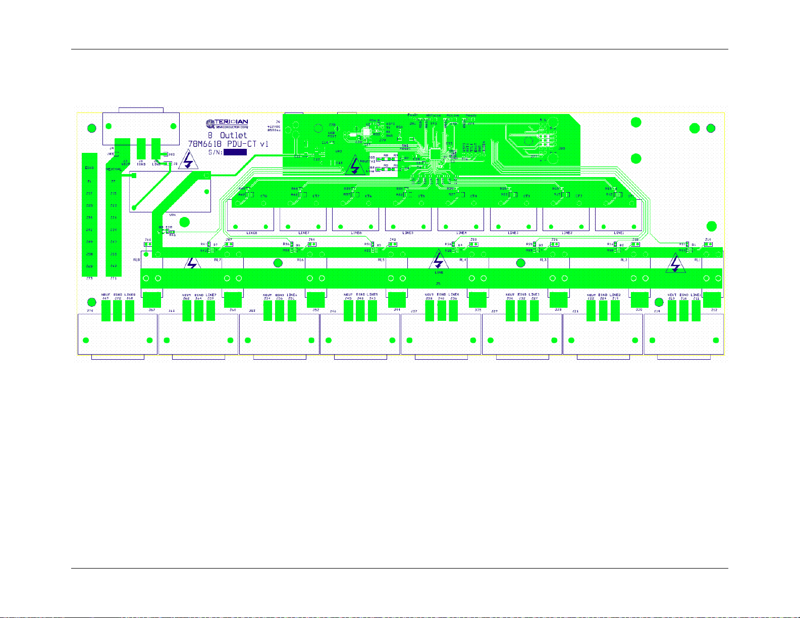
78M6618 PDU1 Evaluation Board User Manual UM_6618_022
A.4 78M6618 PDU-CT Evaluation Board PCB Layouts
Figure 22: 78M6618 PDU-CT Evaluation Board PCB Top View
34 Rev 3
Page 35
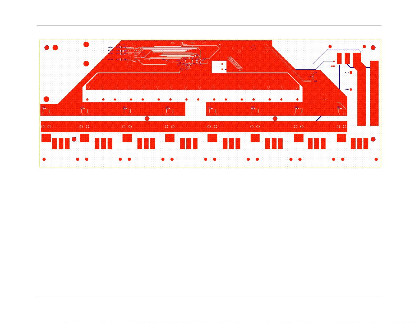
UM_6618_022 78M6618 PDU1 Evaluation Board User Manual
Figure 23: 78M6618 PDU-CT Evaluation Board PCB Bottom View
Rev 3 35
Page 36
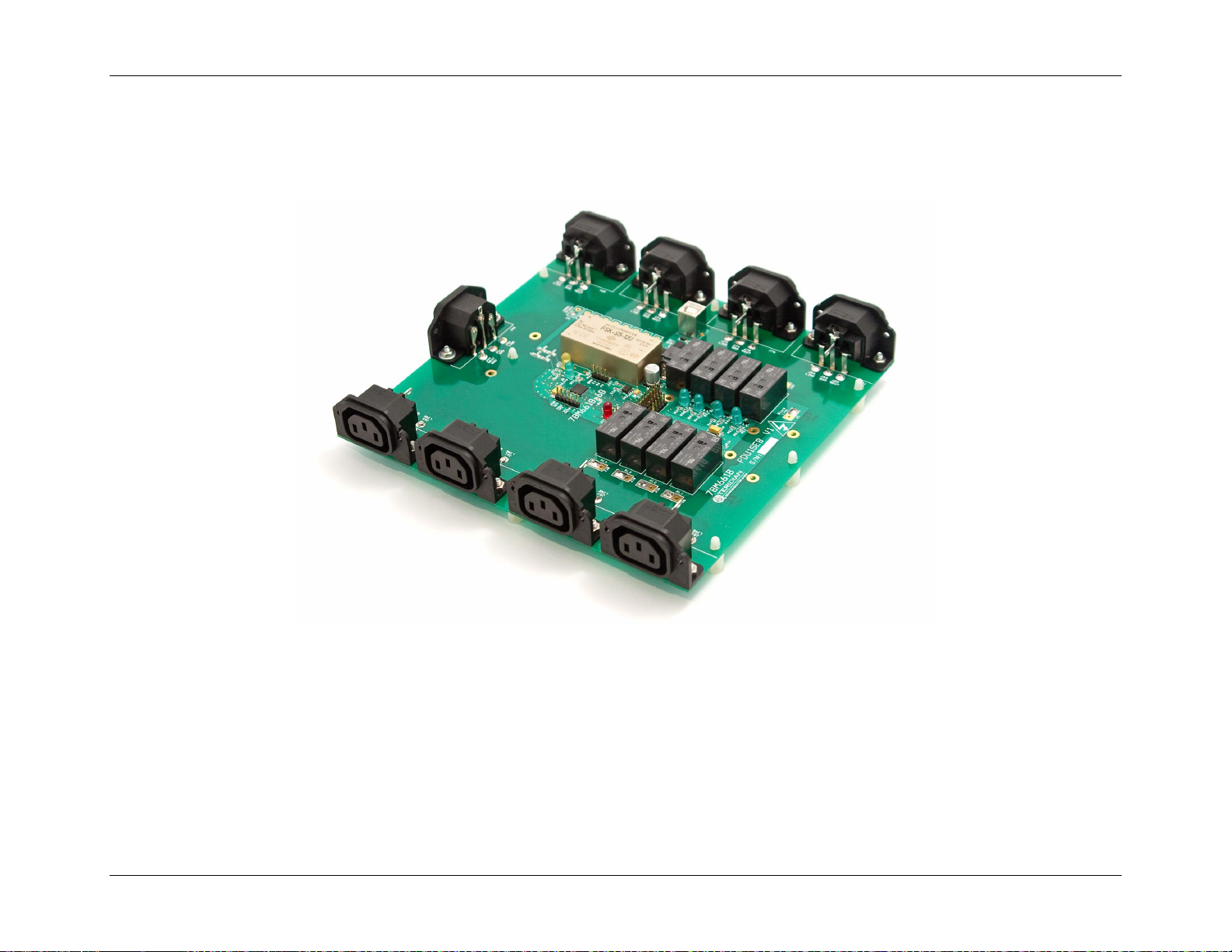
78M6618 PDU1 Evaluation Board User Manual UM_6618_022
Appendix B – 78M6618 PDU1 Version 1 (Single-Ended Shunt)
This appendix includes a photograph of the original 78M6618 PDU1 evaluation board using a single-ended shunt topology. The user
documentation for this board is available by request. This board is no longer available for purchase.
36 Rev 3
Page 37

UM_6618_022 78M6618 PDU1 Evaluation Board User Manual
NUMBER
DATE
Revision History
REVISION
1.0 3/10/2010 First publication.
2.0 9/11
3 11/11
REVISION
Changed the document to reflect the new board revision.
Added Appendix B.
Removed “_DIFF” from “PDU1_DIFF” in all places except where referring
to the board imprint.
Deleted the NI RunTime, LabWindows, and Trouble-Shooting sections.
These sections are no longer applicable.
Corrected Table 1, COM Port Setup Parameters.
Replaced Figure 2 with a new screenshot.
DESCRIPTION
Rev 3 37
 Loading...