

Page 1
71M6521DE/DH/FE
Energy Meter ICs
DATA SHEET
19-5370; Rev 2; 11/11
MPU
RTC
TIMERS
IA
VA
IB
XIN
XOUT
VREF
RX/DIO1
TX/DIO2
V1
TX
RX
COM0..3
V3.3A
V3.3
SYS
VBAT
V2.5
VBIAS
SEG0..18
GNDA GNDD
SEG 24..31/
DIO 4..11
SEG 34..37/
DIO 14..17
ICE
LOAD
88.88.8888
IIC or uWire
EEPROM
POWER
FAULT
AMR
TEST PULSES
COMPARATOR
SENSE
DRIVE/MOD
SERIAL PORTS
OSC/PLL
CONVERTER
DIO, PULSE
COMPUTE
ENGINE
FLASH
RAM
VOLTAGE REF
REGULATOR
POWER SUPPLY
TERIDIAN
71M6521
3.3V LCD
TEMP
SENSOR
32 kHz
A
NEUT
CT/SHUNT
07/25/2007
VB
B
LOAD
IR
PWR MODE
CONTROL
WAKE-UP
BATTERY
ICE_E GNDD
V3P3D
SEG 32,33,
38/ICE
Teridian is a trademark and Single Converter Technology is a registered
GENERAL DESCRIPTION
The Teridian™ 71M6521DE/DH/FE energy meter ICs are highly integrated
systems-on-a-chip (SoCs) with an MPU cor e, RTC, flash, and LCD dri ver.
The Single Converter Technology® with a 22-bit delta-sigma ADC, four
analog inputs, digital temperature compensation, precision voltage
reference, battery voltage monitor, and 32-bit computation engine (CE)
supports a wide range of residential metering applications with very few
low-cost external components. A 32kHz crystal time base for the entire
system and internal battery-backup support for RAM and RTC further
reduce system cost. The ICs support 2-wire, 3-wire, and 4-wire singlephase and dual-phase residential metering along with tamper-detection
mechanisms.
Maximum design flexibility is provided by multiple UARTs, I
MICROWIRE®, up to 18 DIO pins, and in-system programmable flash
memory, which can be updated with data or application code in operation.
A complete array of ICE and deve lopm ent tools , pr ogr am ming l ibr ar ies , and
reference designs enable rapid development and certification of TOU,
AMR, and prepay meters that comply with worldwide electricity metering
standards.
trademark of Maxim Integrated Products Inc.
MICROWIRE is a registered trademark of National Semiconductor Corp.
Rev 2 Page: 1 of 107
2
C,
FEATURES
• Up to 0.1% Wh Accuracy Over 2000:1 Current
Range
• Exceeds IEC 62053/ANSI C 12.20 Standards
• Voltage Reference < 40 ppm/°C (< 20ppm/°C for
71M6521DH)
• Four Sensor Inputs—V
• Low-Jitter Wh and VARh Pulse Test Outputs
(10kHz max)
• Pulse Count for Pulse Outputs
• Four-Quadrant Metering
• Tamper Detection
Neutral Current with CT or Shunt
• Line Frequency Count for RTC
• Digital Temperature Compensation
• Sag Detection for Phase A and B
• Independent 32-Bit Compute Engine
• 46-64Hz Line Frequency Range with Same
Calibration
• Phase Compensation (±7°)
• Battery backup for RTC and battery monitor
• Three Battery Modes with Wake-Up on Pushbutton
or Timer:
Brownout Mode (48µA)
LCD Mode (5.7µA)
Sleep Mode (2.9µA)
• Energy Display on Main Power Failure
• Wake-Up with Pushbutton
• 22-Bit Delta-Sigma ADC
• 8-Bit MPU (80515), 1 Clock Cycle per Instruction
with Integrated ICE for MPU Debug
• RTC with Temperature Compensation
• Auto-Calibration
• Hardware Watchdog Timer, Power-Fail Monitor
• LCD Driver (Up to 152 Pixels)
• Up to 18 General-Purpose I/O Pins
• 32kHz Time Base
• 16KB (6521DE/DH) or 32KB (6521FE) Flash with
Security
• 2KB MPU XRAM
• Two UARTs for IR and AMR
• Digital I/O Pins Compatible with 5V Inputs
• 64-Pin LQFP or 68-Pin QFN Package
• Lead(Pb)-Free Packages
Referenced
DD
Page 2

71M6521DE/DH/FE Data Sheet
Table of Contents
GENERAL DESCRIPTION ........................................................................................................................ 1
FEATURES ................................................................................................................................................ 1
HARDWARE DESCRIPTION ..................................................................................................................... 10
Hardware Overview ..................................................................................................................... 10
Analog Front End (AFE) ............................................................................................................... 10
Input Multiplexer ............................................................................................................ 10
A/D Converter (ADC) ..................................................................................................... 11
FIR Filter ........................................................................................................................ 11
Voltage References ....................................................................................................... 11
Temperature Sensor ...................................................................................................... 12
Battery Monitor .............................................................................................................. 13
Functional Description ................................................................................................... 13
Digital Computation Engine (CE) ................................................................................................. 13
Meter Equations ............................................................................................................ 14
Description ................................................................................................................................... 14
Real-Time Monitor ......................................................................................................... 15
Pulse Generator ............................................................................................................ 15
CE Functional Overview ................................................................................................ 15
80515 MPU Core ........................................................................................................... 17
Memory Organization .................................................................................................... 17
Special Function Registers (SFRs) ................................................................................ 19
Special Function Registers (Generic 80515 SFRs) ....................................................... 20
Special Function Registers Specific to the 71M6521DE/DH/FE .................................... 22
Instruction Set ................................................................................................................ 23
UART ............................................................................................................................. 23
Timers and Counters ..................................................................................................... 25
WD Timer (Software Watchdog Timer) .......................................................................... 28
Interrupts ....................................................................................................................... 30
On-Chip Resources ..................................................................................................................... 38
Oscillator ....................................................................................................................... 38
PLL and Internal Clocks ................................................................................................ 38
Real-Time Clock (RTC) ................................................................................................. 38
Temperature Sensor ...................................................................................................... 38
Physical Memory ........................................................................................................... 39
Optical Interface ............................................................................................................ 40
Digital I/O ....................................................................................................................... 40
LCD Drivers ................................................................................................................... 42
Battery Monitor .............................................................................................................. 42
EEPROM Interface ........................................................................................................ 43
Page: 2 of 107 Rev 2
Page 3

71M6521DE/DH/FE Data Sheet
Hardware Watchdog Timer ............................................................................................ 46
Program Security ........................................................................................................... 46
Test Ports ...................................................................................................................... 47
FUNCTIONAL DESCRIPTION ................................................................................................................... 48
Theory of Operation ..................................................................................................................... 48
System Timing Summary ............................................................................................................. 49
Battery Modes .............................................................................................................................. 50
MISSION ...................................................................................................................................... 51
BROWNOUT Mode ....................................................................................................... 51
LCD Mode ..................................................................................................................... 52
SLEEP Mode ................................................................................................................. 52
Fault and Reset Behavior ............................................................................................................ 57
Wake Up Behavior ....................................................................................................................... 57
Wake on PB................................................................................................................... 58
Wake on Timer .............................................................................................................. 58
Data Flow ..................................................................................................................................... 59
CE/MPU Communication ............................................................................................................. 59
APPLICATION INFORMATION ................................................................................................................. 60
Connection of Sensors (CT, Resistive Shunt) .............................................................................. 60
Distinction between 71M6521DE/71M6521FE and 71M6521DH Parts ....................................... 60
Temperature Measurement ......................................................................................................... 61
Temperature Compensation ........................................................................................................ 61
Temperature Compensation and Mains Frequency Stabilization for the RTC ............................. 64
Connecting 5 V Devices ............................................................................................................... 65
Connecting LCDs ......................................................................................................................... 66
Connecting I2C EEPROMs .......................................................................................................... 68
Connecting Three-Wire EEPROMs ............................................................................................. 69
UART0 (TX/RX) ........................................................................................................................... 69
Optical Interface ........................................................................................................................... 70
Connecting V1 and Reset Pins .................................................................................................... 70
Connecting the Emulator Port Pins .............................................................................................. 71
Crystal Oscillator .......................................................................................................................... 71
Flash Programming ..................................................................................................................... 72
MPU Firmware Library ................................................................................................................. 72
Meter Calibration ......................................................................................................................... 72
FIRMWARE INTERFACE .......................................................................................................................... 73
I/O RAM MAP – In Numerical Order ............................................................................................ 73
SFR MAP (SFRs Specific to the Teridian 80515) – In Numerical Order ...................................... 74
I/O RAM DESCRIPTION – Alphabetical Order ............................................................................ 75
CE Interface Description .............................................................................................................. 82
CE Program ................................................................................................................... 82
Rev 2 Page: 3 of 107
Page 4

71M6521DE/DH/FE Data Sheet
Formats ......................................................................................................................... 82
Constants ...................................................................................................................... 82
Environment .................................................................................................................. 82
CE Calculations ............................................................................................................. 83
CE STATUS .................................................................................................................. 83
CE TRANSFER VARIABLES ........................................................................................ 85
ELECTRICAL SPECIFICATIONS .............................................................................................................. 89
ABSOLUTE MAXIMUM RATINGS .............................................................................................. 89
RECOMMENDED EXTERNAL COMPONENTS ......................................................................... 90
RECOMMENDED OPERATING CONDITIONS .......................................................................... 90
PERFORMANCE SPECIFICATIONS .......................................................................................... 91
INPUT LOGIC LEVELS ................................................................................................. 91
OUTPUT LOGIC LEVELS ............................................................................................. 91
POWER-FAULT COMPARATOR .................................................................................. 91
BATTERY MONITOR .................................................................................................... 91
SUPPLY CURRENT ...................................................................................................... 92
V3P3D SWITCH ............................................................................................................ 92
2.5 V VOLTAGE REGULATOR ..................................................................................... 92
LOW POWER VOLTAGE REGULATOR ....................................................................... 92
CRYSTAL OSCILLATOR .............................................................................................. 93
VREF, VBIAS ................................................................................................................ 93
LCD DRIVERS .............................................................................................................. 94
ADC CONVERTER, V3P3A REFERENCED ................................................................. 94
TEMPERATURE SENSOR ........................................................................................... 95
TIMING SPECIFICATIONS ......................................................................................................... 96
RAM AND FLASH MEMORY ..................................................................................................................... 96
FLASH MEMORY TIMING ............................................................................................ 96
EEPROM INTERFACE .................................................................................................. 96
RESET and V1 .............................................................................................................. 96
RTC ............................................................................................................................... 96
TYPICAL PERFORMANCE DATA ................................................................................ 97
PACKAGE OUTLINE (LQFP 64) ................................................................................................. 98
PACKAGE OUTLINE (QFN 68) ................................................................................................... 98
PINOUT (LQFP-64) ..................................................................................................................... 100
PINOUT (QFN 68) ....................................................................................................................... 100
Recommended PCB Land Pattern for the QFN-68 Package ....................................................... 101
PIN DESCRIPTIONS ................................................................................................................... 102
Power/Ground Pins: ...................................................................................................... 102
Analog Pins: .................................................................................................................. 102
Digital Pins:.................................................................................................................... 103
I/O Equivalent Circuits: .................................................................................................. 104
Page: 4 of 107 Rev 2
Page 5

71M6521DE/DH/FE Data Sheet
ORDERING INFORMATION ...................................................................................................................... 105
REVISION HISTORY ................................................................................................................................. 106
Rev 2 Page: 5 of 107
Page 6

71M6521DE/DH/FE Data Sheet
List of Figures
Figure 1: IC Functional Block Diagram .................................................................................................................................... 9
Figure 2: General Topology of a Chopped Amplifier ............................................................................................................. 11
Figure 3: AFE Block Diagram................................................................................................................................................. 13
Figure 4: Samples from Multiplexer Cycle ............................................................................................................................ 16
Figure 5: Accumulation Interval ............................................................................................................................................ 16
Figure 6: Interrupt Structure ................................................................................................................................................. 37
Figure 7: Optical Interface .................................................................................................................................................... 40
Figure 8: Connecting an External Load to DIO Pins .............................................................................................................. 42
Figure 9: 3-Wire Interface. Write Command, HiZ=0. ............................................................................................................. 44
Figure 10: 3-Wire Interface. Write Command, HiZ=1 ............................................................................................................ 44
Figure 11: 3-Wire Interface. Read Command........................................................................................................................ 45
Figure 12: 3-Wire Interface. Write Command when CNT=0 .................................................................................................. 45
Figure 13: 3-Wire Interface. Write Command when HiZ=1 and WFR=1. .............................................................................. 45
Figure 14: Functions defined by V1 ...................................................................................................................................... 46
Figure 15: Voltage. Current, Momentary and Accumulated Energy ...................................................................................... 48
Figure 16: Timing Relationship between ADC MUX, Compute Engine, and Serial Transfers. ............................................... 49
Figure 17: RTM Output Format ............................................................................................................................................. 49
Figure 18: Operation Modes State Diagram .......................................................................................................................... 52
Figure 19: Functional Blocks in BROWNOUT Mode (inactive blocks grayed out) ................................................................. 53
Figure 20: Functional Blocks in LCD Mode (inactive blocks grayed out) .............................................................................. 54
Figure 21: Functional Blocks in SLEEP Mode (inactive blocks grayed out) .......................................................................... 55
Figure 22: Transition from BROWNOUT to MISSION Mode when System Power Returns .................................................. 56
Figure 23: Power-Up Timing with V3P3SYS and VBAT tied together ................................................................................... 56
Figure 24: Power-Up Timing with VBAT only ....................................................................................................................... 57
Figure 25: Wake Up Timing ................................................................................................................................................... 58
Figure 26: MPU/CE Data Flow ............................................................................................................................................... 59
Figure 27: MPU/CE Communication ..................................................................................................................................... 59
Figure 28: Resistive Voltage Divider (Left), Current Transformer (Right) ............................................................................ 60
Figure 29: Resistive Shunt .................................................................................................................................................... 60
Figure 30: Error Band for VREF over Temperature (Regular-Accuracy Parts) ...................................................................... 62
Figure 31: Error Band for VREF over Temperature (High-Accuracy Parts) ........................................................................... 63
Figure 32: Crystal Frequency over Temperature ................................................................................................................... 64
Figure 33: Crystal Compensation .......................................................................................................................................... 65
Figure 34: Connecting LCDs ................................................................................................................................................. 66
Figure 35: I2C EEPROM Connection ...................................................................................................................................... 68
Figure 36: Three-Wire EEPROM Connection ......................................................................................................................... 69
Figure 37: Connections for the RX Pin .................................................................................................................................. 69
Figure 38: Connection for Optical Components .................................................................................................................... 70
Figure 39: Voltage Divider for V1 .......................................................................................................................................... 70
Figure 40: External Components for RESET: Development Circuit (Left), Production Circuit (Right) .................................. 71
Figure 41: External Components for the Emulator Interface ................................................................................................. 71
Figure 42: Wh Accuracy, 0.1A to 200A at 240V/50Hz and Room Temperature .................................................................... 97
Figure 43: Meter Accuracy over Harmonics at 240V, 30A .................................................................................................... 97
Figure 44: Typical Meter Accuracy over Temperature Relative to 25°C (71M6521FE) ......................................................... 98
Page: 6 of 107 Rev 2
Page 7

71M6521DE/DH/FE Data Sheet
List of Tables
Table 1: Inputs Selected in Regular and Alternate Multiplexer Cycles .................................................................................. 11
Table 2: CE DRAM Locations for ADC Results ...................................................................................................................... 14
Table 3: Meter Equations. .................................................................................................................................................... 14
Table 4: Memory Map ........................................................................................................................................................... 17
Table 5: Stretch Memory Cycle Width .................................................................................................................................. 18
Table 6: Internal Data Memory Map ...................................................................................................................................... 19
Table 7: Special Function Registers Locations ..................................................................................................................... 19
Table 8: Special Function Registers Reset Values ................................................................................................................ 20
Table 9: PSW Register Flags ................................................................................................................................................. 21
Table 10: PSW Bit Functions................................................................................................................................................. 21
Table 11: Port Registers ....................................................................................................................................................... 22
Table 12: Special Function Registers .................................................................................................................................... 23
Table 13: Baud Rate Generation ............................................................................................................................................ 24
Table 14: UART Modes ......................................................................................................................................................... 24
Table 15: The S0CON Register ............................................................................................................................................. 24
Table 16: The S1CON register .............................................................................................................................................. 25
Table 17: The S0CON Bit Functions ..................................................................................................................................... 25
Table 18: The S1CON Bit Functions ..................................................................................................................................... 25
Table 19: The TCON Register .............................................................................................................................................. 26
Table 20: The TCON Register Bit Functions .......................................................................................................................... 26
Table 21: The TMOD Register .............................................................................................................................................. 27
Table 22: TMOD Register Bit Description ............................................................................................................................ 27
Table 23: Timers/Counters Mode Description ...................................................................................................................... 27
Table 24: Timer Modes ......................................................................................................................................................... 28
Table 25: The PCON Register .............................................................................................................................................. 28
Table 26: PCON Register Bit Description ............................................................................................................................. 28
Table 27: The IEN0 Register (see also Table 32) ................................................................................................................. 29
Table 28: The IEN0 Bit Functions (see also Table 32) .......................................................................................................... 29
Table 29: The IEN1 Register (see also Tables 30/31) .......................................................................................................... 29
Table 30: The IEN1 Bit Functions (see also Tables 30/31) ................................................................................................... 29
Table 31: The IP0 Register (see also Table 45) .................................................................................................................... 29
Table 32: The IP0 bit Functions (see also Table 45) ............................................................................................................. 30
Table 33: The WDTREL Register ......................................................................................................................................... 30
Table 34: The WDTREL Bit Functions .................................................................................................................................. 30
Table 35: The IEN0 Register ................................................................................................................................................ 31
Table 36: The IEN0 Bit Functions ......................................................................................................................................... 31
Table 37: The IEN1 Register ................................................................................................................................................ 31
Table 38: The IEN1 Bit Functions ......................................................................................................................................... 31
Table 39: The IEN2 Register ................................................................................................................................................ 32
Table 40: The IEN2 Bit Functions ......................................................................................................................................... 32
Table 41: The TCON Register .............................................................................................................................................. 32
Table 42: The TCON Bit Functions ....................................................................................................................................... 32
Table 43: The T2CON Bit Functions ..................................................................................................................................... 32
Table 44: The IRCON Register ............................................................................................................................................. 33
Table 45: The IRCON Bit Functions ..................................................................................................................................... 33
Table 46: External MPU Interrupts ........................................................................................................................................ 33
Table 47: Interrupt Enable and Flag Bits .............................................................................................................................. 34
Table 48: Priority Level Groups ............................................................................................................................................ 35
Table 49: The IP0 Register ................................................................................................................................................... 35
Table 50: The IP1 Register: .................................................................................................................................................. 35
Table 51: Priority Levels ....................................................................................................................................................... 35
Table 52: Interrupt Polling Sequence .................................................................................................................................... 36
Table 53: Interrupt Vectors ................................................................................................................................................... 36
Table 54: Data/Direction Registers and Internal Resources for DIO Pin Groups .................................................................. 41
Rev 2 Page: 7 of 107
Page 8

71M6521DE/DH/FE Data Sheet
Table 55: DIO_DIR Control Bit ............................................................................................................................................ 41
Table 56: Selectable Controls using the DIO_DIR Bits ........................................................................................................ 42
Table 57: EECTRL Status Bits ............................................................................................................................................. 43
Table 58: EECTRL bits for 3-wire interface ........................................................................................................................ 44
Table 59: TMUX[4:0] Selections .......................................................................................................................................... 47
Table 60: Available Circuit Functions (“—“ means “not active) ............................................................................................ 51
Table 62: VREF Definition for the High-Accuracy Parts ........................................................................................................ 62
Table 63: Frequency over Temperature................................................................................................................................. 64
Table 64: LCD and DIO Pin Assignment by LCD_NUM for the QFN-68 Package ................................................................ 67
Table 65: LCD and DIO Pin Assignment by LCD_NUM for the LQFP-64 Package .............................................................. 68
Page: 8 of 107 Rev 2
Page 9
71M6521DE/DH/FE Data Sheet
IA
VA
MUX
XIN
XOUT
VREF
CKADC
CKTEST/
SEG19
CE
32 bit Compute
Engine
MPU
(80515)
CE
CONTROL
OPT_RX/
DIO1
OPT_TX/
DIO2/
WPULSE/
VARPULSE
RESET
V1
EMULATOR
PORT
CE_BUSY
UART
TX
RX
XFER BUSY
COM0..3
VLC2
LCD DISPLAY
DRIVER
DATA
00-7F
PROG
000-7FF
DATA
0000-FFFF
PROG
0000-7FFF
00007FFF
MPU XRAM
(2KB)
0000-07FF
DIGITAL I/O
CONFIG
2000-20FF
I/O RAM
CE RAM
(0.5KB)
MEMORY SHARE
1000-11FF
RTCLK
RTCLK (32KHz)
MUX_SYNC
CKCE
CKMPU
CK32
CE_E
RTM_E
LCD_E
LCD_CLK
LCD_MODE
DIO
4.9MHz
<4.9MHz
4.9MHz
GNDD
V3P3A
V3P3D
VBAT
VOLT
REG
2.5V to logic
V2P5
MPU_DIV
SUM_CYCLES
PRE_SAMPS
EQU
CKOUT_E
32KHz
TMUXOUT
MPU_RSTZ
FAULTZ
WAKE
TMUX[4:0]
CONFIGURATION
PARAMETERS
GNDA
VBIAS
December 11, 2006
CROSS
CK_GEN
OSC
(32KHz)
CK32
CKOUT_E
MCK
PLL
VREF
VREF_DIS
DIV
ADC
MUX
CTRL
MUX_DIV
CHOP_E
EQU
STRT
IB
MUX
MUX
CKFIR
4.9MHz
RTM
SEG34/DIO14 ..
SEG37/DIO17
WPULSE
VARPULSE
WPULSE
VARPULSE
TEST
TEST
MODE
LCD_MODE
VLC1
VLC0
LCD_E
<4.9MHz
LCD_NUM
DIO_R
DIO_DIR
LCD_NUM
DIO_PV/PW
MUX_ALT
SEG24/DIO4 ..
SEG31/DIO11
SDCK
SDOUT
SDIN
E_RXTX/SEG38
E_TCLK/SEG33
E_RST/SEG32
FLASH
(16/32KB)
FLSH66ZT
V3P3A
FIR_LEN
FIR
SEG0..18
EEPROM
INTERFACE
DIO_EEX
CK_2X
ECK_DIS
V3P3D
LCD_GEN
X4MHZ
PB
RTC
RTC_INC_SEC
RTC_DEC_SEC
VB
VBIAS
MEMORY
SHARE
SEG32,33
SEG19,38
E_RXTX
E_TCLK
E_RST (Open Drain)
ICE_E
DIO1,2
VREF_CAL
∆Σ ADC
CONVERTER
+
-
VREF
ADC_E
RTM_0..3
CE_LCTN
PLS_MAXWIDTH
PLS_INTERVAL
PLS_INV
LCD_BLKMAP
LCD_SEG
LCD_Y
SLEEP
LCD_ONLY
V3P3SYS
TEST
MUX
DIO3,
DIO19/SEG39,
DIO20/SEG40,
DIO21/SEG41
(68 Pin Package Only)
V3P3D
TEMP
VBAT
VBAT
VBIAS
OPTICAL
COMP_STAT
POWER FAULT
OPT_TXE
OPT_TXINV
OPT_RXINV
OPT_RXDIS
MOD
OPT_TXMOD
OPT_FDC
CE_LCTN
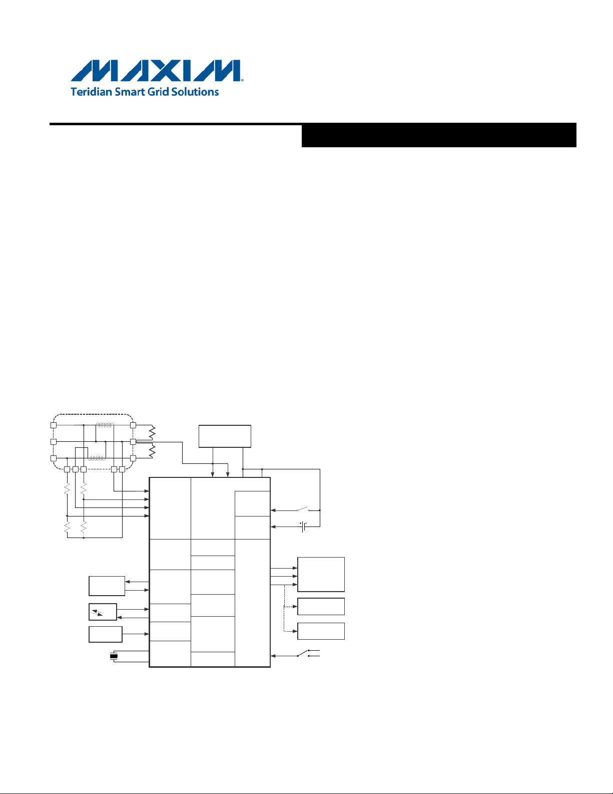
Figure 1: IC Functional Block Diagram
Rev 2 Page: 9 of 107
Page 10

71M6521DE/DH/FE Data Sheet
HARDWARE DESCRIPTION
Hardware Overview
The Teridian 71M6521DE/DH/FE single-chip energy meter integrates all primary functional blocks required to
implement a solid-state electricity meter. Included on chip are an analog front end (AFE), an independent digital
computation engine (CE), a n 8051-compatible microprocessor (MPU) whic h executes one instruction per c lock cycle
(80515), a voltage reference, a tem perature sensor, LC D drivers , RAM, flash memory, a real time clock (RT C), and a
variety of I/O pins. Various current sensor technologies are supported including Current Transformers (CT), and
Resistive Shunts.
In a typical application, the 32-bit compute engine (CE) of the 71M6521DE/DH/FE sequentially processes the
samples from the voltage input s on pins IA, VA, IB, VB and performs calcul ations to measure active energy (Wh),
reactive energy (VARh), A
MPU, processed further and output using the peripheral devices available to the MPU.
In addition to advanced measureme nt functions, the real time cloc k function a llows the 71M 6521DE/DH/FE to record
time of use (TOU) metering infor mation for multi-rate applic ations and to time-stamp tamper event s. Measurements
can be displayed on 3.3V LCD common ly used in low temperature environm ents. Flexible mapping of LCD display
segments will facilitate integrati on of existing custom LCD. Design trade-off bet ween number of LCD segments vs.
DIO pins can be implemented in software to accommodate various requirements.
In addition to the temperature-trimmed ultra-precision voltage reference, the on-chip digital temperature compensation mechanism includes a temper ature sens or and ass ociated cont rols f or correcti on of un wanted temperat ure
effects on measurement and RTC ac curacy, e.g. to meet the requirements of ANSI and IEC standar ds. Temper ature
dependent external compone nts such as cryst al oscillat or, c urrent tra nsfor mers (CT s), and their corres ponding signa l
conditioning circuits can be characterized and their correction factors can be programmed to produce electricity
meters with exceptional accuracy over the industrial temperature r ange.
The 71M6521DH is trimmed at +85°C in addition to the trim at room temperature, which provides a set of
individualized trim fuse values that enable temperature compensation with accuracy better than ±20 PPM/°C.
One of the two internal UARTs is ad apted t o supp ort an Inf rared LED with int ernal dr ive a nd sens e conf igurat ion, a nd
can also function as a standard UART. The optical output can be modulated at 38 kHz. This flexibility makes it
possible to implement AMR meters with an IR interface. A block diagra m of the IC is shown in Figure 1. A det ailed
description of various functional blocks follows.
The AFE of the 71M6521DE/DH/FE is composed of an input multiplexer , a delta-sigma A/D conv erter and a voltage
reference.
2
h, and V2h for four-quadrant metering. These measur ements are then accessed by the
Analog Front End (AFE)
Input Multiplexer
The input multiplexer supports up to four input signals that are applied to pins IA, VA, IB and VB of the device.
Additionally, using the altern ate mux selection, it has the ability to sel ect temperature and the battery voltage. The
multiplexer can be operated in two modes:
• During a normal multiplexer cycle, the signals from the IA, IB, VA, and VB pins are selected.
• During the alternate multiplexer c ycle, the temperature sig nal (TEMP) and the battery monitor are selected,
along with the signal sources sho wn i n Table 1. To prevent unnecessary drainage on the battery, the battery
monitor is enabled only with the BME bit (0x2020[6]) in the I/O RAM.
The alternate mux cycles are usu ally performed infrequently (e.g. every second) by the MPU. In order to prevent
disruption of the voltage track ing PLL and voltage allpass net works, VA is not replaced in the ALT mux sel ections.
Table 1 details the regular and alternative MUX sequences. M i s sing samples due to an ALT multiplexer sequence are
filled in by the CE.
Page: 10 of 107 Rev 2
Page 11
71M6521DE/DH/FE Data Sheet
Regular MUX Sequence
ALT MUX Sequence
Mux State
Mux State
EQU
0 1 2 3 0 1 2
3
G
-
+V
inp
V
outp
V
outn
V
inn
CROSS
A
B
A
B
A
B
A
B
0, 1, 2 IA VA IB VB TEMP VA VBAT
VB
Table 1: Inputs Selected in Regular and Alternate Multiplexer Cycles
In a typical application, IA and IB are c onnected to current transf ormers that sense the current on each phase of the
line voltage. VA and VB are typically connected to voltage sensors thro ugh resistor dividers.
The multiplexer control circuit handles the s etting of the m ultiplexer. T he function of the c ontrol circuit i s governed by
the I/O RAM registers MUX_ALT, MUX_DIV and EQU. MUX_DIV controls the number of samples per cycle. It can
request 2, 3, or 4 multiplexer states per c ycle. Multiplexer states above 4 are reserve d and must not be used. The
multiplexer always starts at the beginning of its list and proceeds until MUX_DIV states have been converted.
The MUX_ALT bit requests an altern ative multiple xer frame. The bi t may be asserted o n any MPU cycle and may be
subsequently de-asserted on an y cycle including t he next one. A ris ing edge on MUX_ALT will cause t he multiplexer
control circuit to wait until the next multiplexer cycle and implement a single alternate cycle.
The multiple xer control circuit also controls the FIR filter initiation a nd the chopping of the ADC reference voltage,
VREF. The multiplexer control circuit is clocked by CK32, the 32768Hz c lock from the PLL bl ock, and launches with
each new pass of the CE program.
A/D Converter (ADC)
A single delta-sigma A/D conver ter digitiz es the vo ltage and c urrent inp uts to the 71M6521DE/DH/FE. The resolution
of the ADC is programmable using th e FIR_LEN regist er as shown in the I/O RAM section. ADC reso lution can be
selected to be 21 bits (FIR_LEN=0), or 22 bit s (FIR_LEN=1). Conversion tim e is t wo cycles of CK 32 with FIR_LEN = 0
and three cycles with FIR_LEN = 1.
In order to provide the maximum resolution, the ADC should be operated with FIR_LEN = 1. Accuracy and
timing specifications in this data sheet are based on FIR_LEN = 1.
Initiation of each ADC conversion is controll ed by th e multipl exer contro l circ uit as descri bed prev iousl y. At the end of
each ADC conversion, the FIR filter out put data is stored into the CE DRAM location de termined by the multiplexer
selection.
FIR Filter
The finite impulse response fi lter is an integral part of the ADC and it is optimized for u se with the multiplexer. The
purpose of the FIR filter is to decim ate the ADC out put to the desir ed resolut ion. At the e nd of each ADC conversion,
the output data is stored into the fixed CE DRAM location determined b y the multiplexer selec tion. FIR data is st ored
LSB justified, but shifted left by nine bits.
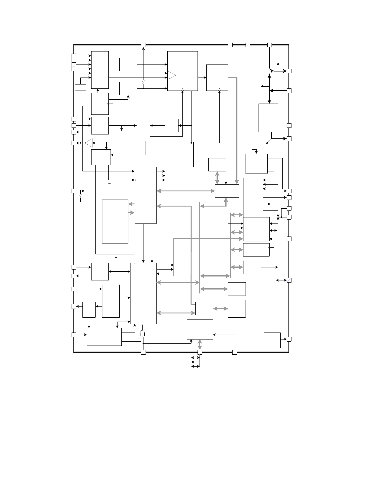
Voltage References
The device includes an on-chip precision bandgap voltage reference that incorporates auto-zero techniques. The
reference is trimmed to minimize errors caused by component mismatch and drift. T he result is a voltage o utput with
a predictable temperature coefficient.
The amplifier within the reference i s chopper stabilized, i.e. the polarit y can be switched by the MPU using the I/O
RAM register CHOP_E (0x2002[5:4]). T he two bits in the CHOP_E register enable the MPU to operate the ch opper
circuit in regular or inverted operation, or in “toggling” mode. When the chopper circuit is toggled in between
multiplexer cycles, DC offsets on the measured signals will automatically be averaged out.
The general topology of a chopped amplifier is given in Figure 2.
Rev 2 Page: 11 of 107
Figure 2: General Topology of a Chopped Amplifier
Page 12

71M6521DE/DH/FE Data Sheet
It is assumed that an offset voltage Voff appears at the positive amplifier input. With all switches, as controlled by
CROSS in the “A” position, the output v oltage is:
Voutp – Voutn = G (Vinp + Voff – Vinn) = G (Vinp – Vinn) + G Voff
With all switches set to the “B” position by applying the inverted CROSS signal, the output voltage is:
Voutn – Voutp = G (Vinn – Vinp + Voff) = G (Vinn – Vinp) + G Voff, or
Voutp – Voutn = G (Vinp – Vinn) - G Voff
Thus, when CROSS is toggled, e. g. after each multiplexer cycle, the offset will alternately appear on t he output as
positive and negative, which results in the offset effectively being eliminated, regardless of its pol ar i ty or magnitude.
When CROSS is high, the hooku p of the amplifier input devices is reversed. This preserves the ove rall polarity of
that amplifier gain; it inverts its input offset . By altern ately r eversing t he conn ection, the amplif ier’s offset i s averag ed
to zero. This removes the most s ignificant long-term drift mechanism in the voltag e reference. The CHOP_E bits
control the behavior of CROSS. The CRO SS signal will reverse the amplifi er connection in the voltage reference i n
order to negate the effects of its offset. On the first CK32 rising edge after the last mux state of its sequence, the mux
will wait one additional CK32 cycle before beginning a new frame. At the beginning of this cycle, the value of CROSS
will be updated according to the CHOP_E bits. The extra CK32 c ycle allows time for the chopped VREF to settle.
During this cycle, MUXSYNC is held high. The leading edge of muxs ync initiates a pass through the CE program
sequence. The beginning of the sequence is the serial readout of the 4 RTM words.
CHOP_E has 3 s tates: positiv e, reverse, and chop. In the ‘positive’ stat e, CROSS is held low. In t he ‘reverse’ state,
CROSS is held high. In t he ‘chop’ stat e, CROSS is toggled near t he end of eac h Mux Frame, as descri bed above. I t
is desirable that CROSS take on alt ernate values at the b eginning of each M ux cycle. For this reas on, if ‘chop’ stat e
is selected, CROSS will not toggle at the end of the last Mux cycle in a SUM cycle.
The internal bias voltage VBIAS (t ypically 1.6 V) is used by the ADC when measuring t he temperature and battery
monitor signals.
Temperature Sensor
The 71M6521DE/DH/FE includes an on-chip temperatur e sensor implemented as a bandgap reference. It is used t o
determine the die temperature The MPU may request an alternate multiplexer cycle containing the temperature
sensor output by asserting MUX_ALT.
The primary use of the temperature data is to determine the magnitude of compensation required to offset the
thermal drift in the system (see secti on titled “Temperature Compensation”).
Page: 12 of 107 Rev 2
Page 13
71M6521DE/DH/FE Data Sheet
IA
VA
MUX
VREF
4.9MHz
VBIAS
CROSS
CK32
VREF
VREF_DIS
MUX
CTRL
MUX_DIV
CHOP_E
EQU
IB
MUX
MUX_ALT
V3P3A
FIR_LEN
FIR
VB
VBIAS
VREF_CAL
∆Σ ADC
CONVERTER
+
-
VREF
ADC_E
TEMP
VBAT
FIR_DONE
FIR_START
Battery Monitor
The battery voltage is measured by the ADC during alternative multiplexer frames if the BME (Battery Measure
Enable) bit in the I/O RAM is set. While BME is set, an on-chip 45kΩ load resistor is applied t o the battery, and a
scaled fraction of the batt ery voltage is a pplied to the ADC input. After ea ch alternative MUX frame, the result of the
ADC conversion is available at CE DRAM address 07. BME is ignored and assumed z ero when system power is not
available (V1 < VBIAS). See the Batter y Monitor section of the Electrical Spec ifications f or details regardin g the ADC
LSB size and the conversion accuracy.
Functional Description
The AFE functions as a data acquisition system, controlled by the MPU. The main signals (IA, VA, IB, VB) are
sampled and the ADC counts obtained are stored in CE DRAM where they can be accessed by the CE and, if
necessary, by the MPU. Alternate m ultiplexer cycles are initiated less f requently by the MPU t o gather access to the
slow temperature and battery signal s .
Figure 3: AFE Block Diagram
Digital Computation Engine (CE)
The CE, a dedicated 32-bit signal process or, performs the precision com putations necessary to accur ately measure
energy. The CE calculations and proces ses include:
• Multiplication of each current s ample with its associated voltage sample to obtain the energ y per sample
(when multiplied with the const ant sample time).
• Frequency-insensitive dela y cancellation on all six channels (to com pensate for th e delay bet ween samples
caused by the multiplexing scheme).
• 90° phase shifter (for VAR calculations).
• Pulse generation.
• Monitoring of the input signal frequency (for frequency and phase inform ation).
• Monitoring of the input signal amplitude (for sag detection).
• Scaling of the processed samples b as ed on calibration coefficients.
The CE program resides in flash memory. Common access to flash memory by CE and MPU is controlled by a
memory share circuit. Each CE instr uction word is two bytes long. Allocated flash space for the CE program cann ot
exceed 1024 words (2KB). The CE program counter begins a pass through the CE code each time multiplexer state 0
begins. The code pass ends when a HALT instruction is executed. For proper operation, the code pass must be
completed before the multiplexer cycle ends (see System Timing Summary in the Functional Descriptio n S ection).
The CE program must begin on a 1Kbyte bo undary of the flash address. The I/O RA M register CE_LCTN[4:0]
defines which 1KB boundary contains the CE code. Thus, the first CE instruction is located at 1024*CE_LCTN[4:0].
The CE DRAM can be accessed by the FIR filter block, the RTM circuit, the CE, and the MPU. Assigned time slots
are reserved for FIR, RTM, and MPU, r es pectively, to prevent bus contention for CE DRAM data access. Holding registers are used to convert 8-bit wide MPU data to/from 32-bit wide CE DRAM data, and wait states are inserted as
needed, depending on the frequency of CKMPU.
Rev 2 Page: 13 of 107
Page 14
71M6521DE/DH/FE Data Sheet
ADDRESS (HEX)
NAME
DESCRIPTION
00
IA
Phase A current
01
VA
Phase A voltage
02
IB
Phase B current
03
VB
Phase B voltage
04
-
Not used
05
-
Not used
06
TEMP
Temperature
07
VBAT
Battery Voltage
Watt & VAR Formula
Element 0
Element 1
1 element, 2W 1φ with neutral current s ense
and tamper detection (VA connected to VB)
1
1 element, 3W 1φ
VA(IA-IB)/2
N/A
2
2 element, 4W 2φ
VA IA
VB IB
The CE DRAM contains 128 32-bit words. The MPU can read and write the CE DRAM as the primary means of data
communication between the two processors .
Table 2 shows the CE DRAM addresses allocated to analog inputs from the AF E .
Table 2: CE DRAM Locations for ADC Results
The CE of the 71M6521DE/DH/FE is aided by suppor t hardware that facilitates im plementation of equations, pulse
counters, and accumulators. This support hardware is controlle d through I/O RAM locations EQU (equation assist),
DIO_PV and DIO_PW (pulse count assist), and PRE_SAMPS and SUM_CYCLES (accumulation assist). PRE_SAMPS
and SUM_CYCLES support a dual level accumulation scheme where the first accumulator accumulate s results from
PRE_SAMPS samples an d the second accumulator acc umulates up to SUM_CYCLES of the first accumulator results.
The integration time for each ener gy output is PRE_SAMPS * SUM_CY CLES/2520.6 ( with MUX_DIV = 1). CE hardware
issues the XFER_BUSY interrupt when the accumulation is complet e.
Meter Equations
Compute Engine (CE) firmware a nd hardware for residential met er configurations implement the eq uations listed in
Table 3. The register EQU (l oc ated i n t he I/ O RAM) specif i es t he equat i on t o be use d b as ed o n the num ber of p has es
used for metering.
EQU
0
Description
VA IA VA IB
Table 3: Meter Equations.
Page: 14 of 107 Rev 2
Page 15

71M6521DE/DH/FE Data Sheet
Real-Time Monitor
The CE contains a Real-Time Monitor (RTM), which can be programmed through the UART to monitor four
selectable CE DRAM locations at f ull sample rate. The four monitored locations ar e serially output to t he TMUXOUT
pin via the digital output multi plexer at the beginning of each CE code pass. T he RTM can be enabled and disabled
with RTM_EN. The RT M output is clocked by CKTEST. E ach RTM word is clocked out in 35 c ycles and contains a
leading flag bit. See the Functional Description section for the RTM output format. RTM is low when not in us e.
Pulse Generator
The chip contains two pulse g enerator s that create l o w-jitt er puls es at a rat e set by either CE or MP U. T he func tion i s
distinguished by EXT_PULSE (a CE input vari able in CE DRAM):
• If EXT_PULSE = 1, APULSEW*WRATE and APULSER*WRATE control the pulse rate (external pulse
generation)
• If EXT_PULSE is 0, APULSEW is repl aced with WSUM_X and APULSER is replaced with VARSUM_X (internal
pulse generation).
The I/O RAM bits DIO_PV and DIO_PW, as described in the Digital I/O section, can be programmed to route
WPULSE to the output pin DIO6 and VAR PULSE to the o utput pi n DIO 7. Pulses c an als o be outp ut on O PT_T X (see
OPT_TXE[1:0] for details).
During each CE code pass, the hard ware stores exported sign bits in an 8-bit FIFO and outputs them at a spec ified
interval. This permits the CE c ode t o c alc ula t e al l of t he pu l se g en erat or o utput s at t he b eginni ng of its code p ass and
to rely on hardware to spread them over the MUX fr ame. The FIFO is reset at the beginning of each MUX frame.
PLS_INTERVAL controls the dela y to the first pulse update and the inter val between subsequent update s. Its LSB is
four CK_FIR cycles, or 4 * 203ns. If PLS_INTERVAL is zero, the FIFO is deactivated and the pulse outputs are
updated immediately. Thus, N
For use with the supplied standard Teridian CE code, PLS_INTERVAL is set to a fixed v alue of 81. PLS_INTERVAL is
specified so that all of the pulse updates are output before
On-chip hardware provides a maximum puls e width feat ure: PLS_MAXWIDTH[7:0] selects a maximum negativ e pulse
width to be ‘Nmax’ updates per multiplexer cycle according to the formula: Nmax = (2*PLS_MAXWIDTH+1). If
PLS_MAXWIDTH = 255, no width checking is performed.
Given that PLS_INTERVAL = 81, the maximum pulse width is determined by:
INTERVAL is 4*PLS_INTERVAL.
the MUX frame completes.
Maximum Pulse Width = (2 * PLS_MAXWIDTH +1) * 81*4*203ns = 65.9µs + PLS_MAXWIDTH * 131.5µs
If the pulse period correspon ding to the pulse rate exceeds the desired pulse width, a squar e wave with 50% dutycycle is generated.
The CE pulse output polarity is progr ammable to be either positiv e or negative. Pulse polarity may be i nverted with
PLS_INV. When this bit is set, the pulses are act i v e hi gh, rather than the more usual active low.
CE Functional Overview
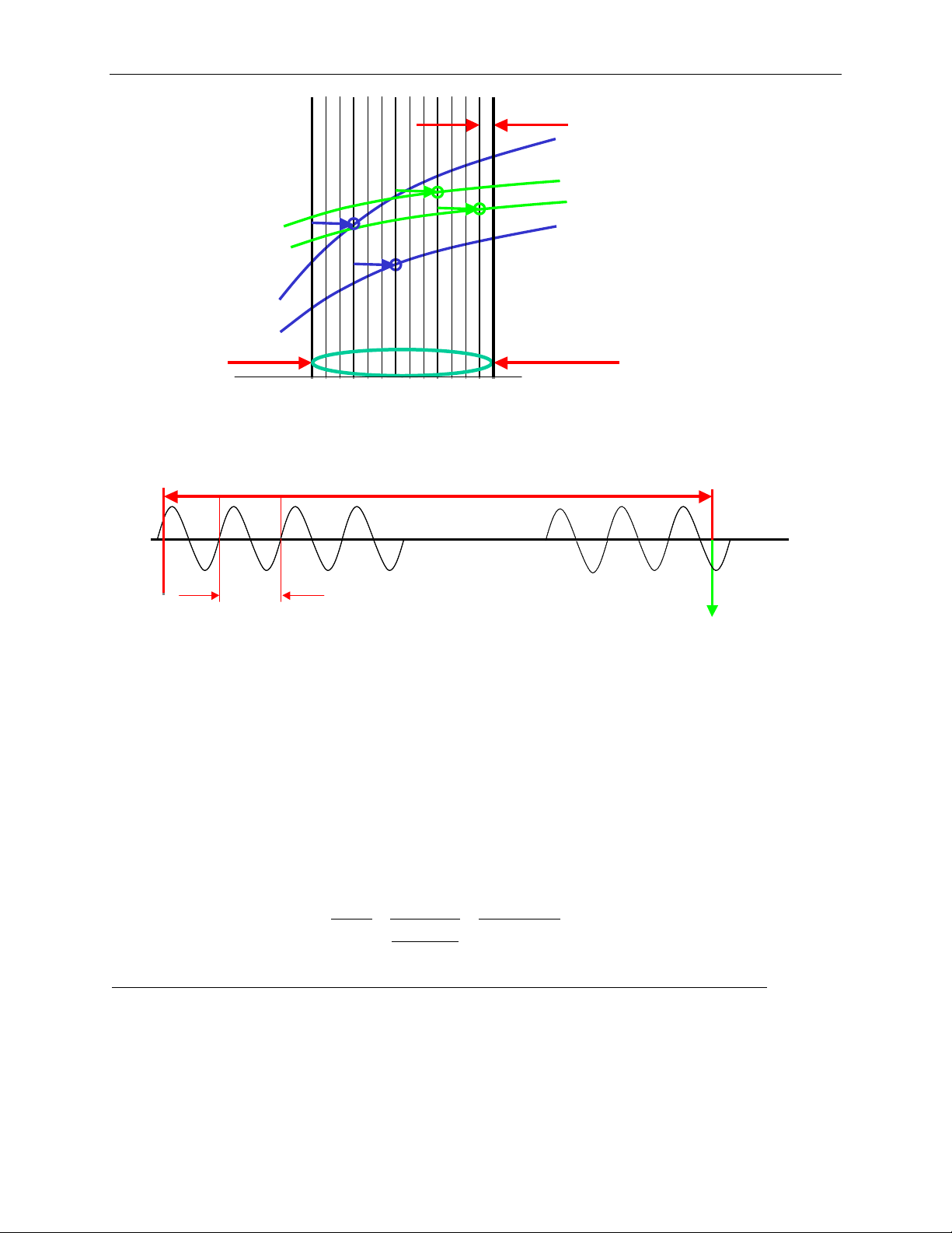
The ADC processes one sample per channel per multiplexer c ycle. Figure 4 shows the timin g of the samples taken
during one multiplexer cycle.
The number of samples processed during one accum ulatio n cycle is controlle d by the I /O RAM r egisters PRE_SAMPS
(0x2001[7:6]) and SUM_CYCLES (0x2001[5:0]). The integration time for each energy output is
PRE_SAMPS * SUM_CYCLES / 2520.6, where 2520.6 is the sample rate [Hz]
For example, PRE_SAMPS = 42 and SUM_CYCLES = 50 will establish 2100 samples per accumulation cycle.
PRE_SAMPS = 100 and SUM_CYCLES = 21 will result in the exact same accumulation cycle of 2100 samples or
833ms. After an accumulation c ycle is completed, the XFER_BUSY interrupt signals to the MPU that accumulated
data are available.
Rev 2 Page: 15 of 107
Page 16
71M6521DE/DH/FE Data Sheet
ms
Hz
Hz
f
N
S
ACC
75.999
62.2520
2520
13
32768
4260==⋅
==
τ
VA
IA
1/32768Hz =
30.518µs
13/327 68Hz = 397µs
per mux cycle
IB
VB
XFER_BUSY
Interrupt to MPU
20ms
833ms
Figure 4: Samples from Multiplexer Cycle
The end of each multiplexer c ycle is signaled to the MPU by the CE_BUSY interru pt. At the end of eac h multiplexer
cycle, status information, suc h as sag data and the digitized input signal , is available to the MPU.
Figure 5: Accumulation Interval
Figure 5 sho ws the accumula tion int erval r esultin g from PRE_SAMPS = 42 and SUM_CYCLES = 50, cons isting of 2100
samples of 397µs each, follo wed by the XFER_BUSY interrupt. The samplin g in this example is applied to a 50Hz
signal.
There is no correlation between the line signal frequency and the choice of PRE_SAMPS or SUM_CYCLES (even
though when SUM_CYCLES = 42 one set of SUM_CYCLES happens to sample a period of 16.6ms). Furthermore,
sampling does not have to start when the line voltage crosses the zero line, and the length of the accumulation
interval need not be an integer multiple of the signal cycles.
It is important to note that the length of the accumulation interval, as determined by N
SUM_CYCLES and PRE_SAMPS, is not an exact multiple of 1000ms. For example, if SUM_CYCLES = 60, and
PRE_SAMPS = 00 (42), the resulting accumulation i nterval is:
, the product of
ACC
This means that accurate time measurements should be based on the RTC, not t he ac cumulation interval.
Page: 16 of 107 Rev 2
Page 17
71M6521DE/DH/FE Data Sheet
Address
0000-7FFF
0000-1FFF
32K
8K
on 1K
boundary
0000-07FF
Static RAM
Volatile
MPU data XRAM,
0
2K
1000-11FF
Static RAM
Volatile
CE data
6
512
Configuration RAM
I/O RAM
80515 MPU Core
The 71M6521DE/DH/FE includes an 8051 5 MPU (8-bit, 8051-compatible) that processes most instruc tions in one
clock cycle. Using a 5 MHz clock results in a processing throughput of 5 MIPS. The 8051 5 architecture eliminates
redundant bus states and implement s parallel executi on of fetch and execution phases. Nor mally a machine cycle i s
aligned with a memory fetch, therefore, most of t he 1-byte instr uctions are perform ed in a single cycl e. This leads t o
an 8x performance (in average) improv ement (in term s of MIPS) over the Int el 8051 d evice r unning at the same cloc k
frequency.
Actual processor clocking speed can be adjusted to the total processing demand of the application (metering
calculations, AMR management, mem ory m anageme nt, L CD driv er managem ent a nd I/O m anagemen t) using t h e I/O
RAM register MPU_DIV[2:0].
Typical measurement and meterin g functions based on the results provided by the internal 32-bit compute engine
(CE) are available for the MPU as part of the Teridian standard library. A standard ANSI “C” 80515-application
programming interface library i s available to help reduce design cycle.
Memory Organization
The 80515 MPU core incorporates the Harvard architecture with separate code and data spaces.
Memory organization in the 80515 is simil ar to that of the industry standard 8051. There are three m emory areas:
Program memory (flash), external data memory (XRAM), physically consisting of XRAM, CE DRAM, and I/O RAM,
and internal data memory (Internal RAM). Table 4 shows the memory map .
Memory
(hex)
0000-3FFF
2000-20FF St atic RAM Volatile
Internal and External Data Memory: Both internal and external data memory are physically located on the
71M6521DE/DH/FE IC. “External” data memory is only external to the 80515 MPU c or e.
Program Memory: The 80515 can theoretically address up to 64KB of program memory space from 0x0000 to
0xFFFF. Program memory is read when the M PU fetches instructions or performs a MOVC operation.
After reset, the MPU starts program e xecution fr om locatio n 0x0000. T he lo wer part of the program memor y includes
reset and interrupt vectors. T he interrupt vectors are spaced at 8-byte int ervals, starting from 0x0003.
External Data Memory: While the 80515 is capable of addressing up to 64KB of external dat a memory (0x0000 to
0xFFFF), only the memory ranges shown in Table 4: Memory Map
contain physical memory. The 80515 writes into e xternal data memor y when t he MPU executes a MOV X @Ri,A o r
MOVX @DPTR,A instruction. The MPU reads external data memory by executing a MOVX A,@Ri or MOVX
A,@DPTR instruction (SFR USR2 provides the upper 8 bytes for the MOVX A,@R i instruction).
Clock Stretching: MOVX instructions can acc ess fast or slo w external RA M and external peripherals. T he three lo w
order bits of the CKCON register def ine the stretch memor y cycles. Setting all th e CKCON stretch bits to one al lows
access to very slow external RAM or external peripherals.
Table 5 shows how the sig na l s of th e E xter n al M em or y Int e rf ace ch an ge w hen s tr etch values are set from 0 to 7. T he
widths of the signals are counted in MPU clo ck cycles. The post-reset state of the CKCO N regis ter , which is in bold in
the table, performs the MOVX instructions with a stretch value equal to 1.
Technology
Flash Memory Non-volatile
Flash Memory Non-volatile CE program 0 2K
Memory Typ e Typical Usage
MPU Program and non-
volatile data
Table 4: Memory Map
Wait States
(at 5MHz)
0
0 256
Memory Size
(bytes)
16K
Rev 2 Page: 17 of 107
Page 18
71M6521DE/DH/FE Data Sheet
0 0 1 1 2 2 3
1
CKCON register Stretch Value Read signals width Write signal width
CKCON.2 CKCON.1 CKCON.0
0 0 0 0 1 1 2 1
0 1 0 2 3 3 4 2
0 1 1 3 4 4 5 3
1 0 0 4 5 5 6 4
1 0 1 5 6 6 7 5
1 1 0 6 7 7 8 6
1 1 1 7 8 8 9 7
Table 5: Stretch Memory Cycle Widt h
There are two types of instructions, differing in whether they prov ide an eight -bit or sixteen-bit indirect address to th e
external data RAM.
In the first type (MOVX A,@Ri), t he cont ents of R0 or R1, in t he curr ent reg i st er bank , pr ov ide the e ig ht lowe r -ordered
bits of address. The eight hi gh-ord ered bit s of ad dress ar e specif ied with the USR2 SFR. This m ethod al lows the user
paged access (256 pages of 256 bytes each) to all ranges of the external data RAM. In the seco nd type of MOVX
instruction (MOVX A,@DPTR), t he data p ointer generates a sixteen-bit ad d ress . This form is faster and more efficient
when accessing very large data arrays (up to 64 Kbytes), since no additional instruct ions are needed to set up the
eight high ordered bits of address.
It is possible to mix the two M OVX types. This provides the user with four separate d ata pointers, two with direct
access and two with paged access to t he entire 64KB of external memory range.
Dual Data Pointer: The Dual Data Pointer accelerates the block moves of data. The standard DPTR is a 16-bit
register that is used to address externa l memor y or perip herals. In th e 80515 c ore, the s tandar d dat a pointer is cal le d
DPTR, the second data pointer is call ed DPTR1. The data pointer select bit chooses t he active pointer. The data
pointer select bit is located at the LSB of the DPS regis ter (DPS.0). DPTR is selected when DPS.0 = 0 and DPTR1 is
selected when DPS.0 = 1.
The user switches between poi nters by to ggling the LSB of t he DPS regis ter. All data poi nter-relat ed instructions use
the currently selected data pointer f or any activity.
The second data pointer may not be supported by certain compilers.
Internal Data Memory: The Internal dat a memory provides 256 bytes (0x00 to 0 xFF) of data memory. The internal
data memory address is always 1 b yte wide and can be ac cessed by either dir ect or in direct addr essing. T he Speci al
Function Registers occupy the upper 128 bytes. This SFR area is available only by direct ad dressing. Indirect
addressing accesses the upper 128 bytes of Internal RAM.
memaddr memrd memaddr memwr
Page: 18 of 107 Rev 2
Page 19
71M6521DE/DH/FE Data Sheet
Address
Direct addressing
Indirect addressing
Special Function Registers
F8
INTBITS
FF
F0
B
F7
E8
WDI
EF
E0
A
E7
D8
WDCON
DF
D0
PSW
D7
C0
IRCON
C7
IEN1
B0
FLSHCTL
PGADR
B7
A8
IEN0
IP0
S0RELL
AF
A0
P2
DIR2
DIR0
A7
IEN2
90
P1
DIR1
DPS
ERASE
97
88
TCON
TMOD
TL0
TL1
TH0
TH1
CKCON
8F
80
P0
SP
DPL
DPH
DPL1
DPH1
WDTREL
PCON
87
Internal Data Memory: The lower 128 bytes contain working re gisters and bit-addressable memory. The lower 3 2
bytes form four banks of eight registers ( R0-R7). Two bits on the program memory status word (PSW) select which
bank is in use. The next 16 bytes form a block of bit-addressable memor y space at bit addressees 0x 00-0x7F. All of
the bytes in the lower 128 b ytes are acces sible t hrough dir ect or indir ect addres sing. Table 6 s hows the int ernal d ata
memory map.
0xFF
0x80
0x7F
0x30
0x2F
0x20
0x1F
0x00
(SFRs)
Byte-addressabl e area
Bit-addressable area
Register banks R0…R7
Table 6: Internal Data Memory Map
Special Function Registers (SFRs)
A map of the Special Function Registers is shown in Table 7.
Hex\Bin
C8
Bit-address-
able
X000 X001 X010 X011 X100 X101 X110 X111
T2CON
Byte-addressable
RAM
Bin/Hex
CF
B8
98
Only a few addresses are oc cupied, the others are not im plemented. SFRs specific to t he 652X are shown in bold
print. Any read access to uni mplemented addresses will return und efined data, while any write acc ess will have no
effect. The registers at 0x80, 0x88, 0x90, etc., are bit-addressable, all others are byte-addressable.
S0CON S0BUF
IP1 S0RELH S1RELH USR2
S1CON S1BUF S1RELL
Table 7: Special Function Registers L ocations
EEDATA EECTRL
BF
9F
Rev 2 Page: 19 of 107
Page 20

71M6521DE/DH/FE Data Sheet
P0
0x80
0xFF
Port 0
SP
0x81
0x07
Stack Pointer
DPL
0x82
0x00
Data Pointer Low 0
DPH
0x83
0x00
Data Pointer High 0
DPL1
0x84
0x00
Data Pointer Low 1
DPH1
0x85
0x00
Data Pointer High 1
WDTREL
0x86
0x00
Watchdog Timer Reload register
PCON
0x87
0x00
UART Speed Control
TCON
0x88
0x00
Timer/Counter Control
TMOD
0x89
0x00
Timer Mode Control
TL0
0x8A
0x00
Timer 0, low byte
TL1
0x8B
0x00
Timer 1, high byte
TH0
0x8C
0x00
Timer 0, low byte
TH1
0x8D
0x00
Timer 1, high byte
CKCON
0x8E
0x01
Clock Control (Stretch=1)
P1
0x90
0xFF
Port 1
DPS
0x92
0x00
Data Pointer select Register
S0CON
0x98
0x00
Serial Port 0, Control Register
S0BUF
0x99
0x00
Serial Port 0, Data Buffer
IEN2
0x9A
0x00
Interrupt Enable Register 2
S1CON
S1BUF
0x9C
0x00
Serial Port 1, Data Buffer
S1RELL
0x9D
0x00
Serial Port 1, Reload Register, low byte
P2
0xA0
0x00
Port 2
IEN0
0xA8
0x00
Interrupt Enable Register 0
IP0
0xA9
0x00
Interrupt Priority Register 0
S0RELL
0xAA
0xD9
Serial Port 0, Reload Register, low byte
IEN1
0xB8
0x00
Interrupt Enable Register 1
IP1
0xB9
0x00
Interrupt Priority Register 1
S0RELH
0xBA
0x03
Serial Port 0, Reload Register, high b yte
S1RELH
0xBB
0x03
Serial Port 1, Reload Register, high b yte
USR2
0xBF
0x00
User 2 Port, high address byte for MOV X@Ri
IRCON
0xC0
0x00
Interrupt Request Control Regis ter
T2CON
0xC8
0x00
Polarity for INT2 and INT3
PSW
0xD0
0x00
Program Status Word
WDCON
0xD8
0x00
Baud Rate Control Register (only W DC ON.7 bit used)
A
0xE0
0x00
Accumulator
B
0xF0
0x00
B Register
Special Function Registers (Generic 80515 SFRs)
Table 8 shows the location of the SFRs and the value they assume at reset or power-up.
Name Location Reset value Description
0x9B 0x00 Serial Por t 1, Control Register
Table 8: Special Function Registers Reset Values
Page: 20 of 107 Rev 2
Page 21
71M6521DE/DH/FE Data Sheet
Bit
Symbol
Function
RS1/RS0
Bank selected
Location
Accumulator (ACC, A): ACC is the accumulator register. Most instructions use the accumulator to hold the
operand. The mnemonics for accumulator-specific instructions refer to accumulator as “A”, no t ACC.
B Register: The B register is used during multiply and divide instructions. It can also be used as a scratch-pad
register to hold temporary data.
Program Status Word (PSW):
MSB LSB
CV AC F0 RS1 RS OV - P
Table 9: PSW Register Flags
PSW.7 CV
PSW.6 AC
PSW.5 F0
Carry flag
Auxiliary Carry flag for BCD operations
General purpose Flag 0 available for user.
F0 is not to be confused with the F0 flag in the CE STATUS register.
PSW.4 RS1 Register bank select control bits. The c ontents of RS1 and RS0 select the working
register bank:
PSW.3 RS0
00 Bank 0 (0x00 – 0x07)
01 Bank 1 (0x08 – 0x0F)
10 Bank 2 (0x10 – 0x17)
11 Bank 3 (0x18 – 0x1F)
PSW.2 OV
PSW.1 PSW.0 P
Overflow flag
User defined flag
Parity flag, affected by hardware to indicate odd / even number of “one” bits in the
Accumulator, i.e. even parity.
Table 10: PSW Bit Functions
Stack Pointer (SP): The stack pointer is a 1-b yte register initialized to 0x07 af ter reset. This register is incremented
before PUSH and CALL instructions, causing the stack to begin at location 0x 08.
Data Pointer: The data pointer (DPTR) is 2 bytes wide. The lower part is DPL, and the high est is DPH. It can be
loaded as two registers (e.g. MOV DPL,#data8). It is generally used to access external code or data space (e.g.
MOVC A,@A+DPTR or MOVX A,@DPTR respectively).
Program Counter: The program counter (PC) is 2 bytes wide initialized to 0x0000 after reset. This register is
incremented when fetching operation c ode or when operating on data from program memory.
Port Registers: The I/O ports are controlle d by Special F unction Register s P0, P1, and P2. The contents of the SFR
can be observed on corresponding pins on the chip. Writing a ‘1’ to any of the ports (see Table 11) causes the
corresponding pin to be at high level (V3P3 ), and writing a ‘0’ causes the corresponding pin to be held at low level
(GND). The data direction regis ters DIR0, DIR1, and DIR2 define indivi dual pins as input or output pins (see section
Digital I/O for details).
Rev 2 Page: 21 of 107
Page 22
71M6521DE/DH/FE Data Sheet
P0
0x80
R/W
Register for port 0 read and write operations (pins DIO4…DIO7)
DIR0
0xA2
R/W
Data direction register for port 0. Setting a bit to 1 means that the corresponding pin is
an output.
P1
0x90
R/W
Register for port 1 read and write operations (pins DIO8…DIO11, DIO14-DIO15)
DIR1
0x91
R/W
Data direction register for port 1.
P2
0xA0
R/W
Register for port 2 read and write operations (pins DIO16…DIO17, DIO19…DIO21)
DIR2
0xA1
R/W
Data direction register for port 2.
ERASE
FLSH_ERASE
0x94
W
Any other pattern written to FLSH_ERAS E will have no effect.
PGADDR
FLSH_PGADR
0xB7
R/W
Must be re-written for each new Page Er ase cycle.
EEDATA
0x9E
R/W
I2C EEPROM interface data register
EECTRL
I2C EEPROM interface control re gister. If the MPU wishes to write a
and then
Register
All DIO ports on the chip are bi-dir ectional. Each of them cons ists of a La tch (SFR ‘P0’ to ‘ P2’), an output dr iver, and
an input buffer, therefore the MPU can out put or read dat a through any of these port s. Even if a DIO pi n is config ured
as an output, the state of the pin c an sti ll b e read b y the MP U, for e xampl e when counti ng puls es iss ued via DIO pins
SFR
Address
that are under CE control.
The technique of reading th e status of or generating interru pts based on DIO pins configure d as outputs,
can be used to implement pulse counting.
R/W Description
Table 11: Port Registers
Special Function Registers Specific to the 71M6521DE/DH/FE
Table 12 shows the location and desc ription of the 71M6521DE/DH/FE-sp ecific SFRs.
Register
Alternative
Name
SFR
Address
R/W Description
This register is used to initiate eit her the Flash Mass Erase cycle or
the Flash Page Erase cycle. Specific patterns are expected for
FLSH_ERASE in order to initiate the appropriate Erase cycle (def ault =
0x00).
0x55 – Initiate Flash Page Erase cycle. Must be preceded by a write
to FLSH_PGADR @ SFR 0xB7.
0xAA – Initiate Flash Mass Erase cycle. Must be preceded by a write
to FLSH_MEEN @ SFR 0xB2 and the debug port must be
enabled.
Flash Page Erase Address register containing the flash memory
page address (page 0 thru 127) that will be erased during the Page
Erase cycle (default = 0x00).
0x9F R/W
Page: 22 of 107 Rev 2
byte of data to EEPROM, it places the data in EEDATA
writes the ‘Transmit’ code t o EECTRL. The write to EECTRL initiates
the transmit sequence. See the EEPROM Interface section for a
description of the command and status bits available for EECTRL.
Page 23
71M6521DE/DH/FE Data Sheet
FLSHCRL
0xB2
WDI
Write 1: Resets the watch dog timer
INTBITS
INT0…INT6
0xF8
R
Interrupt inputs. The MPU may read t hes e bits to see the input to
any memory and are primarily intended for debug use
R/W
R/W
0xE8
R/W
R/W
Bit 0 (FLSH_PWE): Program Write Enable:
0 – MOVX commands refer to XRAM Space, normal operation
(default).
1 – MOVX @DPTR,A moves A to Program Space (Flash) @
DPTR.
This bit is automatically reset aft er each byte written to flash. Writ es
to this bit are inhibited when inter rupts are enabled.
Bit 1 (FLSH_MEEN): Mass Erase Enable:
W
0 – Mass Erase disabled (default).
1 – Mass Erase enabled.
Must be re-written for each new Mass Erase cycle.
Bit 6 (SECURE):
Enables security provisions that prevent external reading of flash
memory and CE program RAM. This bit is reset on chip reset and
may only be set. Attempts to write zero are ignored.
R
Bit 7 (PREBOOT):
Indicates that the preboot sequence is active.
Only byte operations on the whole WDI register
The multi-purpose register WDI cont ains the following bits:
Bit 0 (IE_XFER): XFER Interrupt Flag:
This flag monitors the XFER_BUSY interrupt. It is set by hardware
and must be cleared by the interrupt han dler
Bit 1 (IE_RTC): RTC Interrupt Flag:
W
This flag monitors the RTC_1SEC interrupt. It is set by hardware and
must be cleared by the interrupt handler
Bit 7 (WD_RST): WD Timer Reset:
Read: Reads the PLL_FALL interrupt flag
Write 0: Clears the PLL_FALL interrupt flag
should be used when writing. The byte must have all
bits set except the bits that are to be cleared.
external interrupts INT0, INT1, up t o INT6. These bits do not have
Table 12: Special Function Registers
Instruction Set
All instructions of the generic 805 1 microcontroller are supported. A complete list of the instructi on set and of the
associated op-codes is contained in the 71M6521 Software User’s Guide (SUG).
UART
The 71M6521DE/DH/FE includes a UART (UART 0) that can be program med to communicate with a variety of AMR
modules. A second UART (UART1) is connected to the optical port, as described in the optical port description.
The UARTs are dedicated 2-wi re serial interfaces, which can communicate with an external host processor at up to
38,400 bits/s (with MPU clock = 1.2288MHz). The operation of each pin is as f ol lows:
RX: Serial input data are applied at this pin. Conforming to RS-232 stand ard, the bytes are input LSB first.
TX: This pin is used to output the serial data. The bytes are output LSB first.
The 71M6521DE/DH/FE has several UART-r elated registers for the control and buffering of serial data. All UART
transfers are programmable for parity enable, parity, 2 stop bits/1 stop bit and XON/XOFF options for variable
communication baud rates from 300 to 38400 bps. Table 13 sho ws how the baud rates are calculated. Table 14
shows the selectable UART operation m odes.
Rev 2 Page: 23 of 107
Page 24
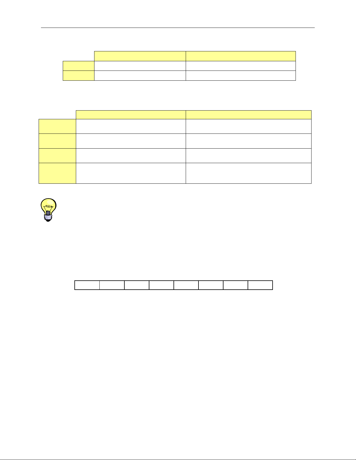
71M6521DE/DH/FE Data Sheet
Using Timer 1
Using Internal Baud Rate Generator
UART 0
UART 1
UART 0
UART 1
smod
2
* f
/ (384 * (256-TH1)) 2
CKMPU
N/A f
Note: S0REL and S1REL are 10-bit values derived by combining bits from the respective timer reload registers. SMOD is the SMOD
bit in the SFR PCON. TH1 is the high byte of timer 1.
smod
* f
CKMPU
/(64 * (210-S0REL))
CKMPU
/(32 * (210-S1REL))
Table 13: Baud Rate Generation
Mode 0
Mode 1
Mode 2
Mode 3
N/A
Start bit, 8 data bits, stop bit, variable baud
rate (internal baud rate generator or timer 1)
Start bit, 8 data bits, parity, stop bit, fixed
baud rate 1/32 or 1/64 of f
CKMPU
Start bit, 8 data bits, parity, stop bit, variable
baud rate (internal baud rate generator or
Start bit, 8 data bits, parity, stop bit, variable baud
rate (internal baud rate generator )
Start bit, 8 data bits, stop bit, variable baud rate
(internal baud rate generator)
N/A
N/A
timer 1)
Table 14: UART Modes
Parity of serial data is avail able through the P flag of the accumulat or. Seven-bit serial modes with parity,
such as those used by the FL AG protoco l, can be simul ated b y setting and re ading bi t 7 of 8-bit outp ut dat a.
Seven-bit serial modes without par ity can be simulated by setting bit 7 to a constant 1. 8-bit serial modes
with parity can be simulated b y setting and reading the 9th bit, using t he control bits TB80 (S0CON.3) and
TB81 (S1CON.3) in the S0COn and S1CON SFRs for transmit and RB81 (S1CON.2) for receive operations.
SM20 (S0CON.5) and SM21 (S1CON.5) can be used as ha ndshake signa ls for inter-proce ssor communicat ion in multi-
processor systems.
Serial Interface 0 Control Register (S0CON).
The function of the UART0 depends on the setting of the Serial Port Control Regi s ter S0CON.
MSB LSB
Serial Interface 1 Control Register (S1CON).
The function of the serial port depends on the setting of the Serial Port Contr ol Register S1CON.
Page: 24 of 107 Rev 2
SM0 SM1 SM20 REN0 TB80 RB80 TI0 RI0
Table 15: The S0CON Register
Page 25
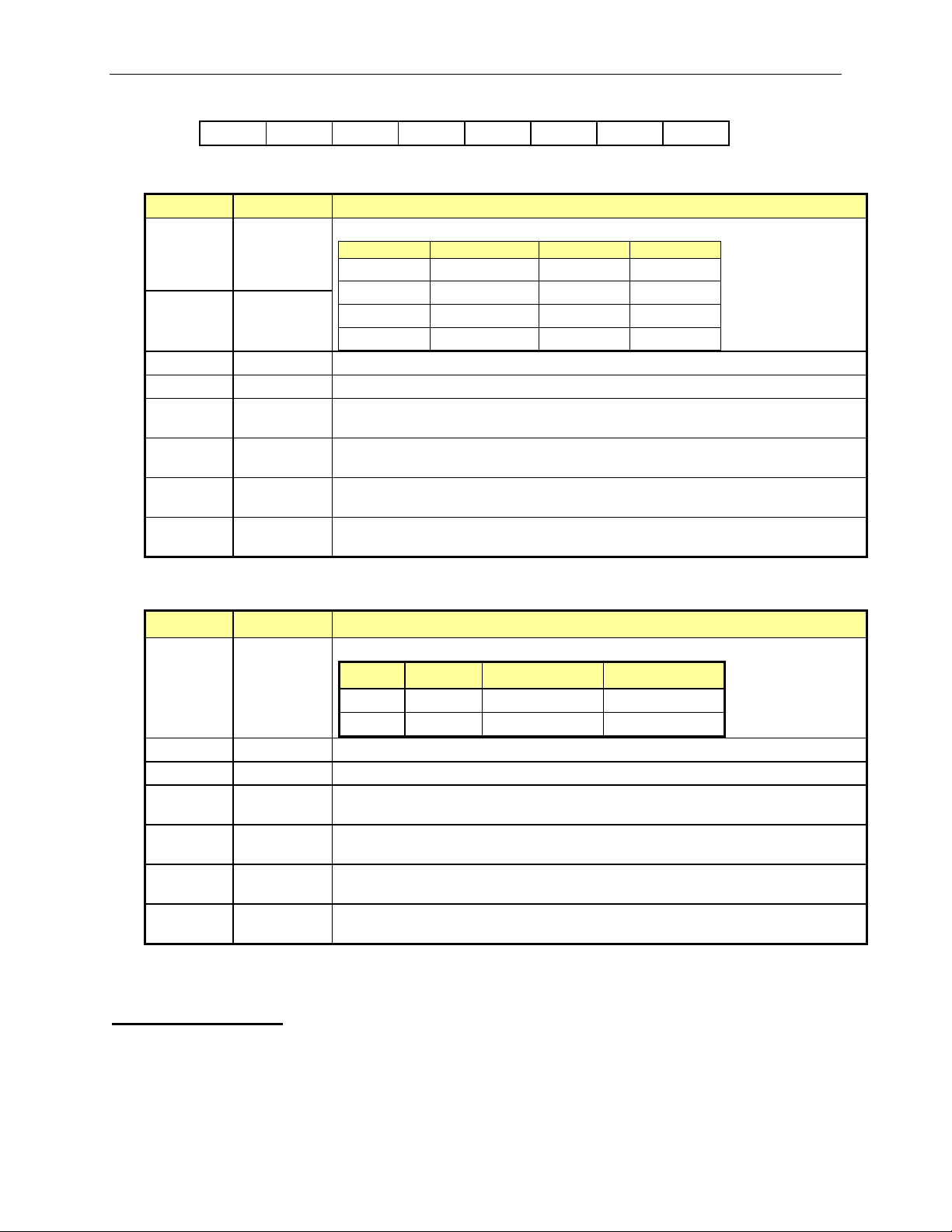
71M6521DE/DH/FE Data Sheet
Bit
Symbol
Function
Mode
Description
SM0
SM1
S0CON.0
RI0
Bit
Symbol
Function
SM
Mode
Description
Baud Rate
MSB LSB
SM - SM21 REN1 TB81 RB81 TI1 RI1
Table 16: The S1CON register
S0CON.7 SM0
These two bits set the UART0 mode:
0 N/A 0 0
S0CON.6 SM1
1 8-bit UART 0 1
2 9-bit UART 1 0
3 9-bit UART 1 1
S0CON.5 SM20
S0CON.4 REN0
S0CON.3 TB80
Enables the inter-processor comm unication feature.
If set, enables serial reception . Cleared by software to disable reception.
The 9th transmitted data bit in Modes 2 and 3. Set or c l ear ed by the MPU, depending
on the function it performs (parity check, multiprocessor communic ation etc.)
S0CON.2 RB80 In modes 2 and 3 it is the 9th data bit received. In Mode 1, if SM20 is 0, RB80 is the
stop bit. In mode 0 this bit is not used. Must be cleared by software
S0CON.1 TI0
Transmit interrupt flag, set by hardware after completion of a serial transfer. Must be
cleared by software.
Receive interrupt flag, set by hardware after completion of a serial reception. Must
be cleared by software
Table 17: The S0CON Bit Functions
S1CON.7 SM
Sets the baud rate for UART1
0 A 9-bit UART variable
1 B 8-bit UART variable
S1CON.5 SM21
S1CON.4 REN1
S1CON.3 TB81
Enables the inter-processor comm unication feature.
If set, enables serial reception . Cleared by software to disable reception.
The 9th transmitted data bit in Mode A. Set or cleare d by the MPU, depending on the
function it performs (parity check , multiprocessor communicati on etc.)
S1CON.2 RB81 In Modes A and B, it is the 9th data bit received. In Mode B, if SM21 is 0, RB81 is the
stop bit. Must be cleared by software
S1CON.1 TI1
Transmit interrupt flag, set by hardware after completion of a serial transfer. Must be
cleared by software.
S1CON.0 RI1
Receive interrupt flag, set by hardware after completion of a serial reception. Must
be cleared by software
Table 18: The S1CON Bit Functions
Timers and Counters
The 80515 has two 16-bit time r/ count er r egis t ers : T i mer 0 a n d T im er 1. These registers can be conf ig ure d for c ounter
or timer operations.
In timer mode, the register is i ncremented every machine cycle meaning that it counts up after ever y 12 periods of the
MPU clock signal.
Rev 2 Page: 25 of 107
Page 26
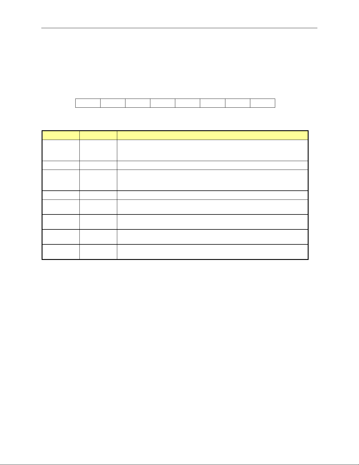
71M6521DE/DH/FE Data Sheet
In counter mode, the register i s incremented when the f alling edge is obser ved at the corresponding i nput signal T0
or T1 (T0 and T1 are the timer gating inputs der ived from certain DIO pins, see t he DIO Ports c hapter). Since it tak es
2 machine cycles to recognize a 1-to-0 ev ent, the maximum input count rate is 1/2 of the oscillator freque ncy. There
are no restrictions on the duty cycle, ho wever to ensure proper recognition of 0 or 1 state, an in put should be stab le
for at least 1 machine cycle.
The timers/counters are controlle d by the TCON Register
Timer/Counter Control Register (TCON)
MSB LSB
TF1 TR1 TF0 TR0 IE1 IT1 IE0 IT0
Table 19: The TCON Register
Bit Symbol Function
The Timer 1 overflow flag is set by hardware when Timer 1 overflows. This flag
TCON.7 TF1
TCON.6 TR1
TCON.5 TF0
TCON.4 TR0
TCON.3 IE1
TCON.2 IT1
TCON.1 IE0
TCON.0 IT0
can be cleared by software and is automat i cally cleared when an interrupt is
processed.
Timer 1 Run control bit. If cleared, Timer 1 stops.
Timer 0 overflow flag set by hard ware when Timer 0 overflows. This flag can be
cleared by software and is automatica l ly cleared when an interrupt is
processed.
Timer 0 Run control bit. If cleared, Timer 0 stops.
Interrupt 1 edge flag is set by hardware when the falling edge on external pin
int1 is observed. Cleared when an interrupt is processed.
Interrupt 1 type control bit. Selects either the falling edge or low level on input
pin to cause an interrupt.
Interrupt 0 edge flag is set by hardware when the falling edge on external pin
int0 is observed. Cleared when an interrupt is processed.
Interrupt 0 type control bit. Selects either the falling edge or low level on input
pin to cause interrupt.
Table 20: The TCON Register Bit Functions
Page: 26 of 107 Rev 2
Page 27
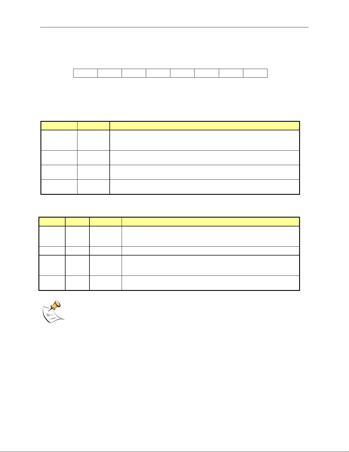
71M6521DE/DH/FE Data Sheet
Bit
Symbol
Function
(x) overflows,
Four operating modes can be selected for Timer 0 and Timer 1. T wo Special Function Registers ( TMOD and TCON)
are used to select the appropriate mode.
Timer/Counter Mode Control register (TMOD):
MSB LSB
GATE C/T M1 M0 GATE C/T M1 M0
Timer 1 Timer 0
Table 21: The TMOD Register
Bits TR1 (TCON.6) and TR0 (TCON.4) in the TCON register (see Table 19 and Table 20) start their associat ed timers
when set.
TMOD.7
TMOD.3
TMOD.6
TMOD.2
TMOD.5
TMOD.1
TMOD.4
TMOD.0
M1 M0
0 0 Mode 0
0 1 Mode 1 16-bit Counter/Timer.
1 0 Mode 2
1 1 Mode 3
Note: In Mode 3, TL0 is affected by TR0 and gate control bits, and sets the TF0 flag on overflow, while
TH0 is affected by the TR1 bit, and the TF1 flag is set on overflow.
Gate
C/T
M1
M0
If set, enables external gate contr ol ( pin int0 or int1 for Counter 0 or 1,
respectively). When int0 or int1 is hi gh, and TRX bit is set (see TCON register), a
counter is incremented every falli ng edge on t0 or t1 input pin
Selects Timer or Counter operation. When set to 1, a Counter operation is
performed. When cleared to 0, the corresponding register will function as a Timer.
Selects the mode for Timer/Counter 0 or Timer/Counter 1, as shown in TMOD
description.
Selects the mode for Timer/Counter 0 or Timer/Counter 1, as shown in TMOD
description.
Table 22: TMOD Register Bit Description
Mode Function
13-bit Counter/Timer with 5 lower bits in the TL0 or TL1 register and the
remaining 8 bits in the TH0 or TH1 register (for Timer 0 and Timer 1,
respectively). The 3 high order bit s of TL0 and TL1 are held at zero.
8-bit auto-reload Counter/Timer. The reload value is kept in TH0 or TH1,
while TL0 or TL1 is incremented every machine cycle. When TL
a value from TH(x) is copied to TL(x).
If Timer 1 M1 and M0 bits are set to '1', Timer 1 stops. If Timer 0 M1 and M0
bits are set to '1', Timer 0 acts as two independent 8-bit Timer/Counters.
Table 23: Timers/Counters Mode Description
Rev 2 Page: 27 of 107
Page 28
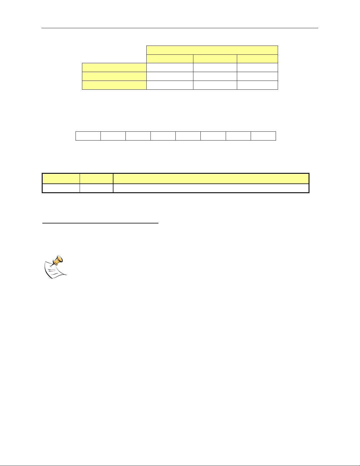
71M6521DE/DH/FE Data Sheet
Timer 0 - mode 1
Timer 0 - mode 2
Bit
Symbol
Function
Table 24 specifies the combinations of operation modes allowed for tim er 0 and timer 1:
Timer 0 - mode 0
Timer/Counter Mode Control register (PCON):
MSB LSB
SMOD
The SMOD bit in the PCON register doubles the baud rate when set.
PCON.7 SMOD
-- -- -- -- -- -- --
Baud rate control.
Table 26: PCON Register Bit Description
Mode 0 Mode 1 Mode 2
YES YES YES
YES YES YES
Not allowed Not allowed YES
Table 24: Timer Modes
Table 25: The PCON Register
Timer 1
WD Timer (Software Watchdog Timer)
The software watchdog timer is a 16-bit counter t hat is inc remented once ever y 24 or 384 c lock cycl es. Aft er a reset,
the watchdog timer is disable d and all registers ar e set to zero. The watchdog consists of a 16-b it counter (WDT), a
reload register (WDTREL), prescaler s (by 2 and by 16), and control l ogic. Once the watchdog is started, it cannot be
stopped unless the internal reset signal becomes active.
Note: It is recommended to use t he hardware watchdog timer inst ead of the software watchdog
timer.
WD Timer Start Procedure: The WDT is started by settin g the SWDT flag. When the WDT register enter s the state
0x7CFF, an asynchronous WDTS signal will become active. The signal WDTS sets bit 6 in the IP0 register and
requests a reset state. WDTS is cleare d ei ther by the reset signal or by changing the state of the WDT timer.
Refreshing the WD Timer: T he watchd og timer must be re freshed reg ularl y to prevent t he reset r equest sig nal from
becoming active. This requirement imposes an obligation on the programmer to issue two instructions. The first
instruction sets WDT and the second inst ruction sets SW DT. The maximum dela y allowed between set ting WDT and
SWDT is 12 cl ock cycles. If this period has expired and SWDT has not been set, the WDT is automatically reset,
otherwise the watchdog timer is reloaded with the content of the WDTREL register and the WDT is automatically
reset. Since the WDT requires exact timing, firmware needs to be designed with special care in order to avoid
unwanted WDT resets. It is strongly discouraged to use the software WDT.
Page: 28 of 107 Rev 2
Page 29
71M6521DE/DH/FE Data Sheet
Bit
Symbol
Function
Bit
Symbol
Function
Special Function Registers for th e WD Timer
Interrupt Enable 0 Register (IEN0):
MSB LSB
EAL WDT ET2 ES0 ET1 EX1 ET0 EX0
Table 27: The IEN0 Register (see also Table 32)
IEN0.6 WDT
Note: The remaining bits in the IE N0 register are not used for watchdog control
Interrupt Enable 1 Register (IEN1):
MSB LSB
EXEN2 SWDT EX6 EX5 EX4 EX3 EX2
IEN1.6 SWDT
Note: The remaining bits in the IEN1 register are not used for watchdog control
Interrupt Priority 0 Register (IP0):
MSB LSB
Watchdog timer refresh flag.
Set to initiate a refresh of the watchdog timer. Must be set directly before SWDT is
set to prevent an unintentional refresh of the watchdog timer. WDT is reset by
hardware 12 clock cycles after it has been set.
Table 29: The IEN1 Register (see also Tables 30/3 1)
Watchdog timer start/refresh flag.
Set to activate/refresh the watchdog timer. When directly set after s etting WDT, a
watchdog timer refresh is performed. Bit SWDT is reset by the hardware 12 clock
cycles after it has been set.
Table 28: The IEN0 Bit Functions (see also Table 32)
Table 30: The IEN1 Bit Functions (see also Tables 30/ 31)
-- WDTS IP0.5 IP0.4 IP0.3 IP0.2 IP0.1 IP0.0
Table 31: The IP0 Register (see also Table 45)
Rev 2 Page: 29 of 107
Page 30
71M6521DE/DH/FE Data Sheet
Bit
Symbol
Function
Bit Symbol Function
IP0.6 WDTS
Note: The remaining bits in the IP0 register are not used for watchdog control
Watchdog Timer Reload Register (WDTREL):
MSB LSB
7 6 5 4 3 2 1 0
Watchdog timer status flag. Set when the watchdog timer was started. Can be
read by software.
Table 32: The IP0 bit Functions (see also Table 45)
Table 33: The WDTREL Register
WDTREL.7
WDTREL.6
to
WDTREL.0
The WDTREL register can be loaded and read at any time.
7
6-0
Prescaler select bit. When set, the watchdog is clocked through an additio nal
divide-by-16 prescaler
Seven bit reload value for the high-b yt e of the watchdog timer. This value i s
loaded to the WDT when a refresh is triggered by a consecutive setting of bits
WDT and SWDT.
Table 34: The WDTREL Bit Functions
Interrupts
The 80515 provides 11 interr upt so urces wit h four pr iorit y l evels. Each source has its o wn request flag(s) located in a
special function register (TCON, IRCON, and SCON).
individually enabled or disabled by the enable bits in SFRs IEN0, IEN1, and IEN2.
External interrupts are the interrupts external to the 80515 core, i.e. signals that originate in other
parts of the 71M6521DE/DH/FE, for example the CE, DIO, RTC EEPROM interface.
Interrupt Overview
When an interrupt occurs, the MPU will vector to the predetermined a ddress as shown in Table 53. Once interrupt
service has begun, it can be interrupted only by a higher priorit y interrupt. The interrupt service is terminated by a
return from instruction, "RET I". When an RETI is performed, the MP U will return to the instruction th at would have
been next when the interrupt occurr ed.
When the interrupt condition oc curs, the MPU will also indic ate this by setting a flag bit. T his bit is set regardless of
whether the interrupt is enabled or disabled. Each interrupt flag is sampled once per machine cycle, then s amples are
polled by the hardware. If the sample indicates a pendi ng interrupt when the interrupt is enabled, then the interru pt
request flag is set.
Each interrupt requested by the corresponding flag can be
Page: 30 of 107 Rev 2
Page 31

71M6521DE/DH/FE Data Sheet
On the next instruction cycle, the inter rupt will be acknowledged by hardware forcing an LCALL to the appropriate
vector address, if the following conditions are met:
• No interrupt of equal or higher priority is already in progress.
• An instruction is currently bein g executed and is not completed.
• The instruction in progress is not RETI or any write access to the registers IEN0, IEN1, IEN2, IP0 or IP1.
Special Function Registers for Interrupts:
Interrupt Enable 0 register (IE0)
MSB LSB
EAL WDT ES0 ET1 EX1 ET0 EX0
Table 35: The IEN0 Register
Bit Symbol Function
IEN0.7 EAL EAL=0 – disable all i nterrupts
IEN0.6 WDT
IEN0.5 IEN0.4 ES0 ES0=0 – disable serial channel 0 interrupt
IEN0.3 ET1 ET1=0 – disable timer 1 overflow interrupt
IEN0.2 EX1 EX1=0 – disable external interrupt 1
IEN0.1 ET0 ET0=0 – disable timer 0 overflow interrupt
IEN0.0 EX0 EX0=0 – disable external interrupt 0
Not used for interrupt control
Interrupt Enable 1 Register (IEN1)
MSB LSB
SWDT EX6 EX5 EX4 EX3 EX2
Bit Symbol Function
IEN1.7 IEN1.6 SWDT
IEN1.5 EX6 EX6=0 – disable external interrupt 6
IEN1.4 EX5 EX5=0 – disable external interrupt 5
IEN1.3 EX4 EX4=0 – disable external interrupt 4
IEN1.2 EX3 EX3=0 – disable external interrupt 3
IEN1.1 EX2 EX2=0 – disable external interrupt 2
IEN1.0 -
Table 36: The IEN0 Bit Functions
Table 37: The IEN1 Register
Not used for interrupt control
Table 38: The IEN1 Bit Functions
Rev 2 Page: 31 of 107
Page 32

71M6521DE/DH/FE Data Sheet
Interrupt Enable 2 register (IE2)
MSB LSB
- - - - - - -
Table 39: The IEN2 Register
Bit Symbol Function
IEN2.0 ES1 ES1=0 – disable serial channel 1 interrupt
Table 40: The IEN2 Bit Functions
Timer/Counter Control register (TCON)
MSB LSB
TF1 TR1 TF0 TR0 IE1 IT1 IE0 IT0
Table 41: The TCON Register
Bit Symbol Function
TCON.7 TF1
TCON.6 TR1
TCON.5 TF0
TCON.4 TR0
TCON.3 IE1
TCON.2 IT1
TCON.1 IE0
TCON.0 IT0
Timer 1 overflow flag
Not used for interrupt control
Timer 0 overflow flag
Not used for interrupt control
External interrupt 1 flag
External interrupt 1 type control bit
External interrupt 0 flag
External interrupt 0 type control bit
ES1
Table 42: The TCON Bit Functions
Timer2/Counter2 Control regist er (T2CON):
Bit Symbol Function
T2CON.7 -T2CON.6 I3FR
T2CON.5 I2FR
TCON.4 …
T2CON0
--
Not used
Polarity control for INT3: 0 - falling edge, 1 – rising edge
Polarity control for INT3: 0 - falling edge, 1 – rising edge
Not used
Table 43: The T2CON Bit Functions
Page: 32 of 107 Rev 2
Page 33

71M6521DE/DH/FE Data Sheet
Interrupt
Interrupt Request register (IRCON)
MSB LSB
EX6 IEX5 IEX4 IEX3 IEX2
Bit Symbol Function
Table 44: The IRCON Register
IRCON.7 IRCON.6 IRCON.5 IEX6
IRCON.4 IEX5
IRCON.3 IEX4
IRCON.2 IEX3
IRCON.1 IEX2
IRCON.0 -
Only TF0 and TF1 (tim er 0 and timer 1 overflow flag) will be autom atically cleared by hardware when the
service routine is called (Signals T0ACK and T1ACK – port ISR – active high when the service routi ne i s
called).
External interrupt 6 edge flag
External interrupt 5 edge flag
External interrupt 4 edge flag
External interrupt 3 edge flag
External interrupt 2 edge flag
Table 45: The IRCON Bit Functions
External Interrupts
The 71M6521DE/DH/FE MPU allows seven external interrupts. These are connected as shown in Table 46. The
direction of interrupts 2 and 3 is pro grammable in the MPU. Interrupts 2 and 3 should be programmed for fall ing
sensitivity. The generic 8051 MPU liter ature states that interrupt 4 through 6 are defined as rising edge sensitive.
Thus, the hardware signals attac hed to interrupts 5 and 6 are inverted to achieve t he edge polarity shown in Table
46.
External
Connection Polarity Flag Reset
0 Digital I/O High Priority
1 Digital I/O Low Priority
2 FWCOL0, FWCOL1 falling automatic
3 CE_BUSY falling automatic
4 PLL_OK (rising), PLL_OK (falling) rising automatic
5 EEPROM busy falling automatic
6 XFER_BUSY OR RTC_1SEC falling manual
Table 46: External MPU Interrupts
FWCOLx interrupts occur when the CE col lides with a flash write attempt. See the flash write description for more
detail.
SFR (special function registe r) enable bits must be set to permit any of these interrup ts to occur. Likewise, each
interrupt has its own flag bit, whic h is set by the int erru pt h ard ware, and r eset b y the MP U interru pt han dler. Not e that
XFER_BUSY, RTC_1SEC, FWCO L0, FWCOL1, PLLRISE , PLLFALL, ha ve their own enab le and flag bits in addition
to the interrupt 6, 4, and 2 enable and flag bits.
IE0 through IEX6 are cleared automatically when the hardware vectors to the interrupt handler. The other flags,
IE_XFER through IE_PB, are cleared by writ ing a zero to them. Since these bits are in a bit-addressable SFR byte,
common practice would be to clear th em with a bit operation. This is to be avoided. T he hardware implements bit
operations as a byte wide read-modify-write hardware macro. If an interrupt occurs after the read, but before the
write, its flag will be cleared unint entionall y. The pr oper way t o clear t he flag bits is to write a byte m ask cons isting of
all ones except for a zero in the locatio n of the bit to be cleared. The flag bit s are configured in hardware to ignor e
ones written to them.
see DIO_Rx
see DIO_Rx
automatic
automatic
Rev 2 Page: 33 of 107
Page 34

71M6521DE/DH/FE Data Sheet
EX0
SFR A8[[0]
IE0
SFR 88[1]
External interrupt 0
EX1
SFR A8[2]
IE1
SFR 88[3]
External interrupt 1
EX2
SFR B8[1]
IEX2
SFR C0[1]
External interrupt 2
EX3
SFR B8[2]
IEX3
SFR C0[2]
External interrupt 3
EX4
SFR B8[3]
IEX4
SFR C0[3]
External interrupt 4
EX5
SFR B8[4]
IEX5
SFR C0[4]
External interrupt 5
EX6
SFR B8[5]
IEX6
SFR C0[5]
External interrupt 6
EX_XFER
2002[0]
IE_XFER
SFR E8[0]
XFER_BUSY interrupt (int 6)
EX_RTC
2002[1]
IE_RTC
SFR E8[1]
RTC_1SEC interrupt (int 6)
IE_FWCOL0
SFR E8[3]
FWCOL0 interrupt (int 2)
IE_FWCOL1
SFR E8[2]
FWCOL1 interrupt (int 2)
IE_PLLRISE
SFRE8[6]
PLL_OK rise interrupt (int 4)
IE_PLLFALL
SFRE8[7]
PLL_OK fall interrupt (int 4)
IE_WAKE
SFRE8[5]
AUTOWAKE flag
IE_PB
SFRE8[4]
PB flag
Interrupt Enable Interrupt Flag
NAME LOCATION NAME LOCATION
EX_FWCOL
EX_PLL
The AUTOWAKE and PB fla g b its are s hown in Table 47 because they behav e sim ilarly to interrupt flags, even t hou g h
they are not actually related to an interr upt. These b its are set by hard ware when the MP U wakes from a push butt on
or wake timeout. The bits are r eset by writi ng a zero. Not e that the PB flag is set whenever t he PB is pushe d, even if
the part is already awake.
Each interrupt has its own flag bit, which is set by the interrupt hard ware and is reset automatically by the MPU
interrupt handler ( 0 through 5 ). XFER_BUS Y and RTC_1S EC, whic h are OR-ed t ogether, have their own e nable and
flag bits in addition to the interrupt 6 enable a nd flag bit s (see Table 47), and t hese interr upts must b e cleared by the
MPU software.
When servicing the XFER_BUSY and RT C_1SEC interrupts, specia l care must be taken to avoid l ockup conditions: If, for example, the XFER_ BUSY interrupt is serviced, contr ol must not return to the m ain
program without checking the RTC_1SEC flag. If this rule is ignored, a RT C_1SEC interrupt appearing
during the XFER_BUSY service rout ine will disable the processing of any XFER_BUSY or RTC_1SEC
interrupt, since both interrupts are edge-triggered (see the Software User’s Guide SUG652X).
The external interrupts are connecte d as shown in Table 47. The polarity of interrupts 2 and 3 is programmable in the
MPU via the I3FR and I2FR bits in T2CON. Interrupts 2 and 3 should be programmed for falling sensitivity. The
generic 8051 MPU literature states that interrupts 4 through 6 are defined as rising edge sensitive. Thus, the
hardware signals attached to interrupts 5 and 6 are inverted to achieve the edge polarity shown in Table 47.
SFR (special function registe r) enable bits must be set to permit any of these interrup ts to occur. Likewise, each
interrupt has its own flag bit that is set by the interrupt hardware and is reset autom atically by the MPU interrupt
handler (0 through 5). XFER_BUSY and RTC_1SEC, which a re OR-ed together, have t heir own enable and flag b its in
addition to the interrupt 6 enabl e and flag bits (see Table 47), and these interrupts must be cleared by the MPU
software.
2007[4]
2007[5]
Table 47: Interrupt Enable and Flag Bits
Interrupt Description
Page: 34 of 107 Rev 2
Page 35

71M6521DE/DH/FE Data Sheet
Group
0
5
Interrupt Priority Level Structure
All interrupt sources are combined in groups, as shown in Table 48:
External interrupt 0 Serial channel 1 interrupt
1
2
3
4
Each group of interrupt sourc es can be programmed individually to one of four priority levels by setting or c learing
one bit in the special function register IP0 and one in IP1.
simultaneously, an internal polling sequence as per Table 52 determines which request is serviced first.
An overview of the interrupt struct ur e i s gi ven in Figure 6.
IEN enable bits must be set to permit any of these interrupt s to occur. Likewise, each interrupt has its own flag bit that
is set by the interrupt hard ware and is reset automati cally by the MPU int errupt handler (0 throu gh 5). XFER_BUSY
and RTC_1SEC, which are OR-ed together, have t heir own enable and flag bits in ad dition to the interrupt 6 enabl e
and flag bits (see Table 47) and these interrupts must be cleared by the MPU software.
Interrupt Priority 0 Register (IP0)
MSB LSB
Timer 0 interrupt - External interrupt 2
External interrupt 1 - External interrupt 3
Timer 1 interrupt - External interrupt 4
Serial channel 0 interrupt - External interrupt 5
- - External interrupt 6
Table 48: Priority Level Groups
If requests of the same priority level are received
-- WDTS IP0.5 IP0.4 IP0.3 IP0.2 IP0.1 IP0.0
Note: WDTS is not used for interrupt controls
Interrupt Priority 1 Register (IP1)
MSB LSB
- - IP1.5 IP1.4 IP1.3 IP1.2 IP1.1 IP1.0
IP1.x IP0.x
0 0 Level0 (lowest)
0 1 Level1
1 0 Level2
1 1 Level3 (highest)
Table 49: The IP0 Register
Table 50: The IP1 Register:
Priority Level
Table 51: Priority Levels
Rev 2 Page: 35 of 107
Page 36

71M6521DE/DH/FE Data Sheet
RI0/TI0
External interrupt 0
Serial channel 1 interrupt
Timer 0 interrupt
External interrupt 2
External interrupt 1
External interrupt 3
Timer 1 interrupt
External interrupt 4
Serial channel 0 interrupt
External interrupt 5
External interrupt 6
Table 52: Interrupt Polling Sequence
Polling sequence
Interrupt Sources and Vectors
Table 53 shows the interrupts with their associated flags and vector addresses.
Interrupt Request Flag Description Interrupt Vector Address
IE0
TF0
IE1
TF1
RI1/TI1
IEX2
IEX3
IEX4
IEX5
IEX6
External interrupt 0 0x0003
Timer 0 interrupt 0x000B
External interrupt 1 0x0013
Timer 1 interrupt 0x001B
Serial channel 0 interrupt 0x0023
Serial channel 1 interrupt 0x0083
External interrupt 2 0x004B
External interrupt 3 0x0053
External interrupt 4 0x005B
External interrupt 5 0x0063
External interrupt 6 0x006B
Table 53: Interrupt Vectors
Page: 36 of 107 Rev 2
Page 37

71M6521DE/DH/FE Data Sheet
IE0
Individual
Interrupt
Flags
RI1
TI1
General
Interrupt
Flags
Internal/
External
Source
>=1
TF0
INT2
IE1
INT3
TF1
INT4
RI0
TI0
>=1
INT5
INT6
IRCON.1
I2FR
IRCON.2
I3FR
IRCON.3
IRCON.4
IRCON.5
IEN0.7
IP1.0/
IP0.0
IP1.1/
IP0.1
IP1.2/
IP0.2
IP1.3/
IP0.3
IP1.4/
IP0.4
IP1.5/
IP0.5
Interrupt
Control
Register
Priority
Assignment
Interrupt
Vector
Polling Sequence
Interrupt
Enable
Logic and
Polarity
Selection
DIO
UART1
(optical)
Timer 0
DIO
Timer 1
CE_BUSY
UART0
EEPROM/
I2C
XFER_BUSY
RTC_1S
IEN0.0
IEN2.0
IEN0.1
IEN1.1
IEN0.2
IEN1.2
IEN0.3
IEN1.3
IEN0.4
IEN1.4
IEN1.5
IE_XFER
IE_RTC
Flash Write
Collision
IE_FWCOL0
IE_FWCOL1
PLL OK
IE_PLLRISE
IE_PLLFALL
Figure 6: Interrupt Structure
Rev 2 Page: 37 of 107
Page 38

71M6521DE/DH/FE Data Sheet
On-Chip Resources
Oscillator
The 71M6521DE/DH/FE oscillator drives a standard 32.768kHz watch crystal. These crystals ar e accurate and do not
require a high-current oscillator c ircuit. The 71M6521DE/DH/FE os cillator has been designed specifically to handle
these crystals and is compatible with their high impedance and limited p ower handling capability.
PLL and Internal Clocks
Timing for the device is derived from the 32.768kHz oscillator output. On-chip timing functions include the MPU
master clock, a real time clock (RTC), and the delta-sigma sample clock. In addition, the MPU has two general
counter/timers (see MPU section).
The ADC master clock, CKADC, is gener ated by an on-chi p PLL. It mult iplies the oscill ator output fr equency (CK32)
by 150.
The CE clock frequency is always CK32 * 150, or 4.9152MHz, where CK32 is the 32kHz clock. The MPU clock
frequency is determined by MPU_DIV and can be 4.9152MHz *2
(MPU_DIV is 0 on power-up). T his makes t he MPU clock scala ble f rom 4.9 152MHz d o wn to 38.4k Hz. The cir cuit also
generates a 2x MPU clock for use b y the emulator. This clock is not generated when ECK_DIS is asserted by the
MPU.
The setting of MPU_DIV is maintained when the device transitions to BROWNOUT mode, but the time base in
BROWNOUT mode is 28,672Hz.
Real-Time Clock (RTC)
The RTC is driven directly by t he crystal osci llator. It is po wered by the n et V2P5NV (batt ery-back ed up supply). The
RTC consists of a counter chain and output registers . The counter chai n consists of sec onds, minutes, hours, day of
week, day of month, month, and year. The RT C is capable of pr ocessi ng leap ye ars. Eac h counter h as it s own output
register. Whenever the MPU r eads the seconds register, al l other output registers are au tomatically updated. Since
the RTC clock is not coherent t o the MPU cl ock, the MPU must read t he s econds r egist er until t wo consecut ive reads
are the same (requires either 2 or 3 reads). At this point, all RTC output registers will have the correct time.
Regardless of the MPU clock speed, R TC reads require one wait state.
RTC time is set by writing to the RTC registe rs in I/ O RAM. Each b yte writt en to RT C must be delayed at least 3 RT C
cycles from any previous byte written to RTC. Hardware RTC write prot ecti on requir es t hat a write to addr ess 0x20 1F
occur before each RTC write. W riting to address 0x2 01F opens a hardware ‘e nable gate’ that rem ains open until an
RTC write occurs and then cl oses . I t is n ot n eces sar y t o dis abl e i nt errupt s between the write operation to 0 x201F an d
the RTC write because the ‘enable gat e’ will remain open until the RTC write finally occurs
Two time correction bits, RTC_DEC_SEC and RTC_INC_SEC are provided to adjust the RT C time. A pulse on one of
these bits causes the time to be decremented or incremented by an additional second at the next update of the
RTC_SEC register. Thus, if the crystal temper ature coefficient is known, the MPU firm ware can integrate tem perature
and correct the RTC time as necessary.
-
MPU_DIV
Hz where MPU_DIV varies from 0 to 7
Temperature Sensor
The device includes an on-chip t emperature sensor for determini ng the temperature of the ban dgap reference. The
MPU may request an alternat e multiplexer frame containing the tem perature sensor output by asserting MUX_ALT.
The primary use of the temperature data is to determine the magnitude of compensation required to offset the
thermal drift in the system (see secti on titled “Temperature Compensation”).
Page: 38 of 107 Rev 2
Page 39

71M6521DE/DH/FE Data Sheet
Physical Memory
Flash Memory: The 71M6521DE/DH/FE includes 16KB ( 71M6521DE/DH) or 32KB (71M6521FE) of on-chip flash
memory. The flash memory primar ily contain s MPU and CE program co de. It also c ontains images of th e CE DRAM,
MPU RAM, and I/O RAM. On power-up, before enabling the CE, the MPU copies t hese images to their respective
locations.
Allocated flash space for the CE program cannot exceed 1024 words (2KB). The CE p rogram must begin on a 1K B
boundary of the flash address . The CE_LCTN[4:0] word defines which 1K B boundary contains the CE code. T hus,
the first CE instruction is located at 1024*CE_LCTN[4:0]. CE_LCTN must be defined before the CE is enabled.
The flash memory is segmented into 512 b yte individually erasable pages.
The CE engine cannot access its program memory when flash write occurs. Thus, the flash write procedur e is to
begin a sequence of flash writ es when CE_ BUSY falls ( CE_BUSY i nterrupt) and to make s ure there i s sufficient time
to complete the sequence before CE_BUSY rises again. The actual time for the flash write operatio n will depend on
the exact number of cycles requi red by the CE program. T ypically (CE program is 512 instructions, mux frame is 13
CK32 cycles), there will be 200µs of flash write time, enough for 4 byt es of flash write. If the CE code is shorter, there
will be even more time.
Two interrupts warn of collisions between the M PU firmwar e and the CE timing. If a flash write is at tempt ed while the
CE is busy, the flash write will not execute and the FW_COL0 interrupt will be issued. If a flash write is still in
progress when the CE would other wise begin a code pass, the cod e pass is sk ipped, th e write i s complet ed, and the
FW_COL1 interrupt is issued.
The bit FLASH66Z (see I/O RAM table) d efines the speed for accessing flash m emory. To minimize supply current
draw, this bit should be set to 1.
Flash erasure is initiated b y writing a specific data pattern to specific SFR registers in t he proper sequence. These
special pattern/sequence requirements prevent inadvertent erasure of the flash memory.
The mass erase sequence is:
1. Write 1 to the FLSH_MEEN bit (SFR address 0xB2[1].
2. Write pattern 0xAA to FLSH_ERASE (SFR address 0x94)
The mass erase cycle can only be initiated when the ICE port is enabled.
The page erase sequence is:
1. Write the page address to FLSH_PGADR (SFR address 0xB7[7: 1]
2. Write pattern 0x55 to FLSH_ERASE (SFR address 0x94)
The MPU may write to the flash memory. This is one of the non-volatile storage options available to the user in
addition to external EEPROM.
FLSH_PWE (flash program write ena ble) dif ferent iates 8051 5 data store instructions (MOVX@DPTR,A) between flash
and XRAM writes.
Updating individual bytes in fl as h memory:
The original state of a flash byt e is 0xFF (all ones). Onc e, a value other than 0xFF is written to a f lash memory cell,
overwriting with a different va l ue usually requires that the c ell is erased first. Since cells c annot be erased individually,
the page has to be copied to RAM, followed b y a page erase. After this, the page can be upd ated in RAM and then
written back to the flash memory.
MPU RAM: The 71M6521DE/DH/FE includes 2k-bytes of static RAM memory on-chip (XRAM) plus 256-bytes of
internal RAM in the MPU core. The 2K-bytes of static RAM are used for data s torage during normal MPU operations.
CE DRAM: The CE DRAM is the working d ata memory of the CE (128 32-bit words). The MPU can read and write
the CE DRAM as the primary means of dat a c ommunication between the two proces s ors.
Rev 2 Page: 39 of 107
Page 40

71M6521DE/DH/FE Data Sheet
B
A
OPT_TXINV
from OPT_TX UART
MOD
EN DUTY
OPT_TX
OPT_TXMOD
OPT_FDC
OPT_TXE[1:0]
1
2
V3P3
Internal
A B
OPT_TXMOD=0
OPT_TXMOD=1,
OPT_FDC=2 (25%)
B
A
1/38kHz
0
2
3
DIO2
WPULSE
VARPULSE
Optical Interface
The device includes an interf ace to implement an IR/optical port. The pin OPT _Tx is designed to directly drive a n
external LED for transmitting data o n a n o pti cal l ink . The pin OPT_RX is d esig ned t o se ns e the inp ut f ro m an e xt erna l
photo detector used as the receiver f or the optical link. These two pins are connected to a dedicated UART port
(UART1).
The OPT_TX and OPT_RX pins can be inverted with configuration bits OPT_TXINV and OPT_RXINV, respectively.
Additionally, the OPT_TX out put ma y be mo dulated at 3 8kHz. Modul atio n is ava ilabl e whe n system po wer is prese nt
(i.e. not in BROWNOUT mode). The OPT_TXMOD bit enables modul ation. Dut y cycle is c ontrolled b y OPT_FDC[1:0],
which can select 50%, 25%, 12.5%, and 6. 25% duty cycl e. 6.25% duty cyc le means OPT_T X is low for 6.25% of th e
period. Figure 7 illustrates the OPT_TX generator.
When not needed for the optical UART, the OPT_TX pin can alternatively be configured as DIO2, WPULSE, or
VARPULSE. The configuration bits are OPT_TXE[1:0]. Likewise, OPT _RX can alter n atel y be c onfig ure d as DIO _1. I ts
control is OPT_RXDIS.
Digital I/O
The device includes up to 18 pins (QFN 68 pack age) or 14 pins (LQFP 64 package) of general pur pose digital I/O.
These pins are compatible with 5 V inputs (no current-limiting resistors are needed). Som e of them are dedicated DIO
(DIO3), some are dual-function that can alternatively be used as LCD drivers (DIO4-11, 14-17, 19-21) and som e
share functions with the optical port (DIO1, DIO2). On reset or power-up, all DIO pins are inputs until they are
configured for the desired dir ection under M PU control. The pi ns are configured by the DIO register s and by the fiv e
bits of the LCD_NUM register (locate d in I/O RAM). Once dec lared as DIO , each pin c an be co n figur ed indepe ndentl y
as an input or output with the DIO_DIRn bits. A 3-bit configuration word, DIO_Rx, can be used for cert ain pins, when
configured as DIO, to individually assig n an int erna l reso ur c e such as an i nt err upt or a t i mer contr ol. Table 54 lists the
direction registers and config urability ass ociated with eac h group of DIO pins . Table 55 shows the c onfiguration f or a
DIO pin through its associated bit in its DIO_DIR register.
Tables showing the relationship between LCD_NUM and the available segment/DIO pins can be found in the
Applications section and in the I /O RAM Description under LCD_NUM[4:0].
Figure 7: Optical Interface
Page: 40 of 107 Rev 2
Page 41

71M6521DE/DH/FE Data Sheet
DIO
PB 1 2 3 4 5 6 7 8 9 10
11
12
13
14
15
Pin no. (64 LQFP)
62
57 3 -
37
38
39
40
41
42
43
44
--
--
20
21
Pin no. (68 QFN)
65
60 3 5
39
40
41
42
43
44
45
46
--
--
21
22
0 1 2 3 4 5 6 7 0 1 2 3 --
-- 6 7
DIO0=P0 (SFR 0x80)
DIO1=P1 (SFR 0x90)
0 1 2 3 4 5 6 7 0 1 2 3 --
-- 6 7
DIO_DIR0 (SFR 0xA2)
DIO_DIR1 (SFR 0x91)
Internal Resources
Configurable
DIO
16
17
18
19
20
21
22
23
Pin no. (64 LQFP)
22
12
--
--
--
--
--
--
Pin no. (68 QFN)
23
13
--
24
47
68
0 1 -- 3 4 5 --
--
DIO2=P2 (SFR 0xA0)
0 1 -- 3 4 5 --
--
DIO_DIR2 (SFR 0xA1)
Internal Resources
Configurable
DIO Pin n Function
Data Register
Direction Register
Y Y Y Y Y Y Y Y Y Y Y Y -- -- -- --
Data Register
Direction Register
N N -- N N N -- --
Table 54: Data/Direction Registers and Internal Resources for DIO Pin Groups
DIO_DIR [n]
0 1
Input Output
Table 55: DIO_DIR Control Bit
Additionally, if DIO6 and DIO 7 are declared out puts, they can be c onfigured as dedi cated pulse output s (WPULSE =
DIO6, VARPULSE = DIO7) using DIO_PW and DIO_PV registers. I n this case, DIO6 an d DIO7 are under CE control.
DIO4 and DIO5 can be configured to implement the EEPROM Interface.
The PB pin is a dedicated digital input. If the optical UART is not used, OPT_TX and OPT _RX can be configured as
dedicated DIO pins (DIO1, DIO2, s ee Optical Interface section).
A 3-bit configuration word, I/O RA M register, DIO_Rx (0x2009[2:0] through 0x20 0E[6:4]) c an be used for certain pins ,
when configured as DIO, to in dividuall y assign an i nternal re source such as an inter rupt or a t imer contro l (see Table
54 for DIO pins available for this opt ion). This way, DIO pins can be tracked even if they are configured as output s.
Tracking DIO pins configured as outputs is useful for pulse counting without external hardware.
When driving LEDs, relay coils etc. , the DIO pins should sink the current into GNDD (as shown in
Figure 8, right), not source it from V3P3D (as shown in Figure 8, left). This is du e to the resistance
of the internal switch that connects V3P3D to either V3P3SYS or VBAT.
When configured as inputs, the dual-function (DIO/SEG) pins should not be pulled above V3P3SYS
in MISSION and above VBAT in LCD and BROWNOUT modes. Doing so will distort the LCD
waveforms of the other pins. This limitation applies to any pin that can be configured as a LCD
driver.
The control resources selectabl e for the DIO pins are listed i n Table 56. If more than one in put is connected to the
same resource, the resources are combined using a logical OR.
The PB pin is a dedicated digital input. In addition, if the optical UART is not used, OPT_TX and OPT_RX can be
configured as dedicated DIO pins. Thus, in addition to the 16 general-purpose DIO pins (DIO4…DIO11,
DIO14…DIO21), there are three additional pins that can be used for digital input and out put.
Rev 2 Page: 41 of 107
Page 42

71M6521DE/DH/FE Data Sheet
Recommended
R
LED
DIO1
V3P3D
71M6521
V3P3SYS
DGND
VBAT
3.3V
Recommended
R
LED
DIO1
V3P3D
71M6521
V3P3SYS
DGND
VBAT
3.3V
Value
Resource Selected for DIO Pin
Not recommended
71M6521
DIO1
R
V3P3D
LED
V3P3SYS
3.3V
DGND
VBAT
71M6521
DIO1
R
V3P3D
LED
V3P3SYS
3.3V
DGND
VBAT
Figure 8: Connecting an External Load to DIO Pins
DIO_R
0 NONE
1 Reserved
2 T0 (counter0 clock)
3 T1 (counter1 clock)
4 High priority I/O interrupt (INT0 rising)
5 Low priority I/O interrupt (INT1 rising)
6 High priority I/O interrupt (INT 0 falling)
7 Low priority I/O interrupt (INT1 falling)
Table 56: Selectable Controls usin g the DIO_DIR Bits
LCD Drivers
The device in the 68-pin QFN pac kage contains 20 dedicated LCD segm ent drivers in addition to the 18 multi -use
pins described above. Thus, the device i s capable of driving bet ween 80 to 152 pixels of LCD display with 25% duty
cycle (or 60 to 114 pixels with 33% duty cycle). At eight pixels per digit, this corresponds to 10 to 19 digits.
The device in the 64-pin LQFP package c ontains 20 dedicated LCD seg ment drivers in addition to the 15 mu lti-use
pins described above. Thus, the device i s capable of driving bet ween 80 to 140 pixels of LCD display with 25% dut y
cycle (or 60 to 105 pixels with 33% duty cycle). At eight pixels per digit, this corresponds to 10 to 17 digits.
The LCD drivers are grouped int o four commons a nd up to 38 segm ent drivers (68-p in package), or 4 commons an d
35 segment drivers (64-pin pa ckage). The LCD i nterface is f lexible and can dr ive either d igit segments o r enunciator
symbols.
Segment drivers SEG18 and SEG19 can b e configured t o blink at either 0.5Hz or 1Hz. The blink rate i s controll ed by
LCD_Y. There can be up to four pixels/segments connected to each of these drivers. LCD_BLKMAP18[3:0] and
LCD_BLKMAP19[3:0] identify which pixels, if any, ar e to blink.
LCD interface memory is powered by the non-volatile supply. The bits of the LCD memory are
preserved in LCD and SLEEP modes, even if their pin is not configured as SEG. In this case, they can
be useful as general-purpose nonvolatile storage.
Battery Monitor
The battery voltage is measured by the ADC duri ng alternative MU X frames if the BME (Battery Measur e Enable) bit
is set. While BME is set, an on-chip 45kΩ load resistor is applied to the battery and a sc aled fraction of the batter y
voltage is applied to the ADC input. After each alternative MUX f r ame, the result of the ADC conversion is available at
CE DRAM address 0x07. BME is ignored and assumed zer o when system power is not available. See the B attery
Monitor section of the Electrical Specification section for details regarding the ADC LSB size and the conversion
accuracy.
Page: 42 of 107 Rev 2
Page 43

71M6521DE/DH/FE Data Sheet
7
ERROR
R 0 Positive
1 when an illegal command is received.
6
BUSY
R 0 Positive
1 when serial data bus is busy.
5
RX_ACK
R
1
Negative
0 indicates that the EEPROM sent an ACK bit.
4
TX_ACK
R
1
Negative
0 indicates when an ACK bit has been sent to the EEPROM
CMD
Operation
0001
Receive a byte from EEPROM and send ACK .
0011
Transmit a byte to EEPROM.
0101
Issue a ‘STOP’ sequence.
0110
Receive the last byte from EEPROM, do not send ACK.
1001
Issue a ‘START’ sequence.
Others
No Operation, set the ERROR bit.
EEPROM Interface
The 71M6521DE/DH/FE provides h ardware support for either type of EEP ROM interface, a two-pin interface and a
three-pin interface. The interfaces use the EECTRL and EEDATA registers for communication.
Two-Pin EEPROM Interface
The dedicated 2-pi n serial int erface communic ates with e xternal EEPRO M devices. T he interface is multiplexed o nto
pins DIO4 (SCK) and DIO5 (SDA) controlled by the DIO_EEX bit I/O RAM (see I/O RAM Table). The MPU
communicates with the interface thr ough two SFR regist ers: EEDATA and EECTRL. If the MPU wishes to write a byte
of data to EEPROM, it places the data in EEDATA and t hen writes the ‘Transmit’ command (CMD = 001 1) to EECTRL.
This initiates the transmit oper ation. The transmit operati on is finished when the BUSY bit falls. Interrupt INT5 is als o
asserted when BUSY falls. The MPU can then check the RX_ACK bit to see if the EEPROM acknowledged the
transmission.
A byte is read by writing the ‘Receiv e’ command (CMD = 000 1) to EECTRL and waiting for the BUSY bit to fall. Upo n
completion, the received dat a is in EEDATA. The seri al tran smit and rec eive c lock is 78k Hz dur ing e ach t ransmiss ion ,
and the clock is held in a high state unt il the next transmission. The bits in EECTRL are shown in Table 57.
The EEPROM interface can also be operated by controlling the DIO4 and DIO5 pins directly (“bit-banging”).
However, controlling DIO4 and DIO5 directly is discouraged, because it may tie up the MPU to the point
where it may become too busy to process interrupts.
Status
Bit
3-0
Name
CMD[3:0
]
Read/
Write
W 0
Reset
State
Polarity Description
0000
No-op. Applying the no-op command will s top the I2C clock
(SCK, DIO4). Failure to issue the no-op command will keep
the SCK signal toggling.
Positive,
see CMD
Table
Table 57: EECTRL Status Bits
Rev 2 Page: 43 of 107
Page 44

71M6521DE/DH/FE Data Sheet
Control
Bit
Wait for Ready. If this bit is set, t he trailing edge of BUSY will be delayed
ignored if HiZ=0.
Asserted while serial data bus is busy. When the BUSY bit falls, an INT5
interrupt occurs.
Indicates that the SD signal is to made high impedance immediately after
the last SCK rising edge.
4
RD
W
Indicates that EEDATA is to be filled with data from E EPROM.
Specifies the number of clocks to be is s ued. Allowed values are 0
SDATA will simply obey the HiZ bit.
SCLK (output)
BUSY (bit)
CNT Cycles (6 shown)
SDATA (output)
Write -- No HiZ
D2D3D4D5D6D7
EECTRL Byte Written
INT5
SDATA output Z
(LoZ)
CNT Cycles (6 shown)
Write -- Wi th HiZ
INT5
EECTRL Byte Written
SCLK (output)
BUSY (bit)
SDATA (output)
D2D3D4D5D6D7
(HiZ)(LoZ)
SDATA output Z
Three-Wire EEPROM Interface
A 500kHz three-wire interface, using S DATA, SCK, and a DIO pin for CS is available. The interface is selected with
DIO_EEX=3. The same 2-wire EECTRL register is used, except the bits are reconfigured, as shown in Table 58. When
EECTRL is written, up to 8 bits from EEDATA are either written to the EEPROM or read from the EEPROM, depending
on the values of the EECTRL bits.
Name Read/Write Description
until a rising edge is seen on the data l ine. This bit can be used during
7
WFR
W
the last byte of a Write command to cause t he INT5 interrupt to occur
when the EEPROM has finished its internal write sequence. This bit is
6
5
BUSY
HiZ
R
W
through 8. If RD=1, CNT bits of data will be read MSB first, and right
3-0
CNT[3:0]
W
justified into the low order bits of EEDATA. If RD=0, CNT bits will be sent
MSB first to EEPROM, shifted out of EEDATA’s MSB. If CNT is zero,
Table 58: EECTRL bits for 3-wire interface
The timing diagrams in Figure 9 through Figure 13 describe the 3-wire E EPROM interface behavior. A ll commands
begin when the EECTRL regi ster is written. Transactions start by first rai sing the DIO pin that is connected to CS.
Multiple 8-bit or less commands such as those shown in Figure 9 through Figure 13 are then sent via EECTRL and
EEDATA. When the transaction is finished, CS must be lower ed. At the end of a Read transact ion, the EEPROM will
be driving SDATA, but will tr ansition to HiZ (high impe dance) when CS falls. The firm ware should then immediatel y
issue a write command with CNT=0 and H iZ=0 to take control of SDATA and force it to a low-Z state.
Figure 9: 3-Wire Interface. Write Command, HiZ=0.
Figure 10: 3-Wire Interface. Write Command, HiZ=1
Page: 44 of 107 Rev 2
Page 45

71M6521DE/DH/FE Data Sheet
CNT Cycles (8 shown)
READ
D0D1D2D3D4D5
INT5
D6D7
EECTRL Byte Written
SCLK (output)
BUSY (bit)
SDATA (input)
SDATA output Z
(HiZ)
CNT Cycles (0 shown)
Write -- No HiZ
D7
INT5 not issued
CNT Cycles (0 shown)
Write -- HiZ
INT5 not issued
EECTRL Byte Written EECTRL Byte Written
SCLK (output)
BUSY (bit)
SDATA (output)
SCLK (output)
BUSY (bit)
SDATA (output)
(HiZ)
SDATA output ZSDATA output Z
(LoZ)
CNT Cycles (6 shown)
Write -- With HiZ and WFR
EECTRL Byte Wri t ten
SCLK (output)
BUSY (bit)
SDATA (out/in)
D2D3D4D5D6D7
BUSY READY
(From EEPROM)
INT5
(From 6520)
SDATA output Z
(HiZ)(LoZ)
Figure 12: 3-Wire Interface. Write Command when CNT=0
Figure 11: 3-Wire Interface. Read Command.
Figure 13: 3-Wire Interface. Write Command when HiZ=1 and WFR=1.
Rev 2 Page: 45 of 107
Page 46

71M6521DE/DH/FE Data Sheet
V3P3
V3P3 400mV
V3P3 - 10mV
VBIAS
0V
Battery
modes
Normal
operation,
WDT
enabled
WDT dis-
abled
V1
Hardware Watchdog Timer
In addition to the basic watchdog timer included in the 80515 MPU, an
independent, robust, fixed-duration, watchdog timer (WDT) is included in the
device. It uses the RTC crystal osci llator as its time base and must be r efreshed
by the MPU firmware at least every 1.5 s econds. When not refreshed on time the
WDT overflows, and the part is reset as if the RE SET pin were pull ed h ig h, exc ept
that the I/O RAM bits will be i n the same sta te as after a wake-up from SLEEP or
LCD modes (see the I/O RAM description for a list of I/O RAM bit states after
RESET and wake-up). 4100 osc illator cycles (or 125m s) after the WDT over flow,
the MPU will be launched from program address 0x0000.
A status bit, WD_OVF, is set when WDT overflow occurs. This bit is po wered by
the non-volatile supply and can be read b y the MPU to determine if the part is
initializing after a WDT over flow event or after a power-up. After it is read, MPU
firmware must clear WD_OVF. The WD_OVF bit is cleared by the RESET pin
There is no internal digital state t hat deactivates the WDT. For debug pur poses,
however, the WDT can be disabled by tying the V1 pin to V3P3 (see Figure 39).
Of course, this also deactivates V1 power fault detection. Since there is no
method in firmware to disable the c rystal oscillator or the WDT, it is gu aranteed
that whatever state the part might f ind itself in, upon WDT overflo w, the part will
be reset to a known state.
Asserting ICE_E will also de activate the WDT. This is the only method th at will
disable the WDT in BROWNOUT mode.
In normal operation, the WDT is reset by periodically writing a one to the
WDT_RST bit. The watchdog timer is also reset when the internal signal WAKE=0 (s ee s ection on Wake Up Behavior).
Figure 14: Functions defined by V1
Program Security
When enabled, the security feature lim its the ICE to global flash erase op erations only. All other ICE oper ations are
blocked. This guarantees the s ecurity of the user’s MPU and CE program code. Security is enabled by MPU cod e
that is executed in a 32 cycle preboot interval before the primary boot sequence b egins. Once security is enabled, the
only way to disable it is to perform a global erase of the flash, followed by a c hi p r eset.
The first 32 cycles of the MPU boot co de are calle d t he pr eb oot ph ase bec ause duri ng th i s phase the ICE is inhibited.
A read-only status bit, PREBOOT, ident ifies these cycles to the MPU. Upon completion of preboot, the I CE can be
enabled and is permitted to take control of the MPU.
SECURE, the security enable bit, is reset whenever the chip is r eset. Hardware associated with the bit permits only
ones to be written to it. Thus, preboot c ode m ay set SECURE to enable the security featu re but m ay not r eset it. Onc e
SECURE is set, the preboot code is protected and no external read of program code is p ossible
Specifically, when SECURE is set:
• The ICE is limited to bulk flash erase only.
• Page zero of flash memory, the preferred l ocation for the user’s preboot c ode, may not be page-erased b y
either MPU or ICE. Page zero may only be erased with global flash erase.
• Writes to page zero, whether by MPU or ICE are inh ibi ted.
The SECURE bit is to be used with caution! Inadvertently setting this bit will inhi bit access to the p art via
the ICE interface, if no mechanism for actively resetting the part between reset and erase operations is
provided (see ICE Interface description).
Page: 46 of 107 Rev 2
Page 47

71M6521DE/DH/FE Data Sheet
0
Analog
DGND 1 Analog
Reserved
2
Analog
DGND
3-5
Analog
Reserved
6
Analog
VBIAS 7 Analog
Not used
8-0x0F
--
Reserved
0x10 – 0x13
--
Not used
0x14
Digital
RTM (Real time output from CE)
0x15
Digital
WDTR_EN (Comparator 1 Output AND V1LT3)
0x16 – 0x17
Not used
0x18
Digital
RXD (from Optical interface, w/ opt ional inversion)
0x19
Digital
MUX_SYNC
0x1A
Digital
CK_10M (10MHz clock)
0x1B
Digital
CK_MPU (MPU clock)
0x1C
--
Reserved
0X1D
Digital
RTCLK (output of the oscillator ci r cuit, nominally 32,786Hz)
0X1E
Digital
CE_BUSY (busy interrupt generated by CE, 396µs)
nominally every 999.7ms)
Test Ports
TMUXOUT Pin: One out of 16 digital or 8 analog s ignals can be selected to be output on the TMUXOUT pin. The
function of the multiplexer is controlled with the I/O RAM register TMUX (0x20AA[4:0]), as shown in Table 59.
TMUX[4:0] Mode Function
0X1F Digital
XFER_BUSY (transfer busy interrupt generated by CE,
Table 59: TMUX[4:0] Selections
Rev 2 Page: 47 of 107
Page 48

71M6521DE/DH/FE Data Sheet
∫
=
t
dttItVE
0
)()(
22
QP +
-500
-400
-300
-200
-100
0
100
200
300
400
500
0 5 10 15 20
Current [A]
Voltage [V]
Energy per Interval [Ws]
Accumulated Energy [Ws]
FUNCTIONAL DESCRIPTION
Theory of Operation
The energy delivered by a power source into a load can be expressed as:
Assuming phase angles are constant, the following formulae apply:
P = Real Energy [Wh] = V * A * cos φ* t
Q = Reactive Energy [VARh] = V * A * sin φ * t
S = Apparent Energy [VAh] =
For a practical meter, not o nly voltage and current amplitudes, but also phase angles and harmonic content may
change constantly. Thus, simple RM S me as urem e nts ar e i nher entl y in acc urat e. A moder n s oli d-st ate el ect ric it y met er
IC such as the Teridian 71M6521DE/DH/FE functions by emulating the integr al operation above, i.e. it processes
current and voltage samples through a n ADC at a constant frequency. As long as th e ADC resolution i s high enough
and the sample frequency is be yond the harmonic range of interes t, the current and voltage sam ples, multipl ied with
the time period of sampling will yield an accurate quantity for the moment ary energy. Summing up the momentary
energy quantities over time will res ult in accumulated energy.
Figure 15 shows the shapes of V(t), I(t), the momentary power and the accumulated power, resulting from 50
samples of the vol tage and c urrent si gnals over a period of 20ms. T he applicat ion of 24 0VAC and 100A resu lts in a n
accumulation of 480Ws (= 0.133Wh) over the 20ms period, as indicated by the A ccumulated Power curve.
The described sampling method works reliably, even in the presence of dynamic phase shift and harmonic dist ortion.
Page: 48 of 107 Rev 2
Figure 15: Voltage. Current, Momentary and Accumulated Energy
Page 49

71M6521DE/DH/FE Data Sheet
CKTEST
TMUXOUT/RTM
FLAG
RTM DATA0 (32 bits)
LSB
SIGN
LSB
SIGN
RTM DATA1 (32 bits)
LSB
LSB
SIGN
SIGN
RTM DATA2 (32 bits)
RTM DATA3 (32 bits)
0 1 30 31 0 1 30 31 0 1 30 31 0 1 30 31
FLAG
FLAG
FLAG
MUX_SYNC
CK32
CK32
MUX STATE
0
MUX_DIV Conversions, MUX_DIV=1 (4 conversions) is shown
Settle
ADC MUX Frame
ADC EXECUTION
S
MUX_SYNC
S
CE_EXECUTION
RTM
140
MAX CK COUNT
0 450
150
900 1350 1800
ADC0 ADC1 ADC2 ADC3
CK COUNT = CE_CYCLES + flo or(( CE _ CYCLES + 2) / 5)
NOTES:
1. ALL DIMENSIONS ARE 5MHZ CK COUNTS.
2. THE PRECISE FREQUENCY OF CK IS 150*CRYSTAL FREQUENCY = 4.9152MHz.
3. XFER_BUSY OCCURS ONCE EVERY (PRESAMPS * SUM_CYCLES) CODE PASSES.
CE_BUSY
XFER_BUSY
INITIATED BY A CE OPCODE AT END OF SUM INTERVAL
ADC TIMING
CE TIMING
RTM TIMING
1 2 3
System Timing Summary
Figure 16 summarizes the timing relationships between the input MUX states, the CE_BUSY signal, and the t wo
serial output streams. In this example, MUX_DIV=4 and FIR_LEN=1 (384). The duratio n of each MUX frame is 1 +
MUX_DIV * 2 if FIR_LEN=288, and 1 + MUX_DIV * 3 if FIR_LEN=384. An ADC conversion will always consume an
integer number of CK32 clock s. Followed by the conversi ons is a single CK32 cycle where the bandgap voltage is
allowed to recover from the change in CROSS.
Each CE program pass begins when ADC0 (channel IA) conversion begins. Depending on the length of the CE
program, it may continue run ning until the e nd of the ADC3 (VB) conversion. CE o pcodes are const ructed to ensure
that all CE code passes consume exactl y the same number of cycles. The result of each ADC convers ion is inserte d
into the CE DRAM when the conversion is complete. The CE code is written t o t olerat e su dden c ha nges in A DC dat a.
The exact CK count when each ADC value is loaded into DRAM is shown in Figure 16.
Figure 16 also shows that the serial RTM data stream begins transmitting at the beginning of state ‘S.’ RTM,
consisting of 140 CK cycles, will a lways finish before the next code pass s tarts.
Figure 16: Timing Relationship between ADC MUX, Compute Engine, and Serial Transfers.
Figure 17: RTM Output Format
Rev 2 Page: 49 of 107
Page 50

71M6521DE/DH/FE Data Sheet
Battery Modes
Shortly after system power (V3P3SYS) is applied, t he part will be i n MISSIO N mode. MISSION m ode means that the
part is operating with syste m power and that the internal PLL is stable. T his mode is the normal operation mode
where the part is capable of measuri ng energy.
When system power is not available (i.e. when V1<VB IAS), the 71M6521DE/DH/FE can be in on e of three battery
modes, i.e. BROWNOUT, LCD, or SLEEP mode. As s oon as V1 f alls b elo w VBIAS or whe n the par t wakes u p unde r
battery power (with suffici ent voltage margin), the part will automatically enter BROWNOUT mode (see Wake Up
Behavior section). From BROWN OUT mode, the MPU ma y enter either LCD m ode or SLEEP mode b y setting either
the LCD_ONLY or SLEEP I/ O RAM bits ( only one b it can be set at the s ame time in B ROWNOUT mode, since s etting
one bit will already force the part into SLEEP or LCD mode, disabling the M PU).
Figure 18 shows a state diagram of the various operation modes, with the possible transit ions between modes. For
information on the timing of mode transitions refer to Figure 22 through Figure 24.
Meters that do not require function ality in the battery modes , e.g. meters that only use the S LEEP mode to
maintain the RTC, still need t o contain code that br ings the chip from BR OWNOUT mode to SLEEP m ode.
Otherwise, the chip remains in BR OWNOUT mode, o nce the system power is m issing, an d consumes m ore
current than intended.
Similarly, meters equipped with batteries need to cont ain code that transitions t he chip to SLEEP mode as
soon as the battery is attached in production. Otherwise, remaining in BROWNOUT mode would add
unnecessary drain to the battery.
The transition from MISSION mode to BROWNOUT mode is signaled by the IE_PLLFALL interrupt flag (in SFR
0xE8[7]). The transition in th e other direction is signaled by the IE_PLLRISE interrupt flag (S FR 0xE8[6]), when the
PLL becomes stable.
Transitions from both LCD and SLEEP mode back to BROWNOUT mode are initiated by wake-up timer timeout
conditions or pushbutton events. W hen the PB pin is pulled high (pushbutton is pressed), the IE_PB interrupt flag
(SFR 0xE8[4]) is set, and when the wake-up timer times out, the IE_WAKE interrupt flag (SFR 0xE8[5]) is set.
In the absence of system power, if the voltage margin for the LDO re gulator providing 2.5 V to t he internal circuitry
becomes too low to be safe, the par t aut omat ically enters s leep m ode (B AT _OK f alse). The b atter y volt age must sta y
above 3V to ensure that BAT_OK remains t rue. Under this c ondition, the 71M6521DE/DH/FE stays in SLEEP mode,
even if the voltage margin for the LDO improves (BAT_OK true).
Table 60 shows the circuit functions available in each operating mode.
Page: 50 of 107 Rev 2
Page 51

71M6521DE/DH/FE Data Sheet
System Power
Battery Power (Non-volatile Supply)
MISSION
CE
Yes
--
--
--
CE Data RAM
Yes
Yes
--
--
FIR
Yes
--
--
--
PLL, ADC, VREF, BME etc
4.92MHz
(from PLL)
28.672kHz
(7/8 of 32768Hz)
MPU_DIV
Yes
--
--
--
ICE
Yes
Yes
--
--
DIO Pins
Yes
Yes
--
--
Watchdog Timer
Yes
Yes
--
--
LCD
Yes
Yes
Yes
--
EEPROM Interface (2-wire)
Yes
Yes (8kb/s)
--
--
EEPROM Interface (3-wire)
Yes
Yes (16kb/s)
--
--
UART
Yes
Yes
--
--
Optical TX modulation
Yes
--
--
--
Flash Read
Yes
Yes
--
--
Flash Page Erase
Yes
Yes
--
--
Flash Write
Yes
--
--
--
RAM Read and Write
Yes
Yes
--
--
Wakeup Timer
Yes
Yes
Yes
Yes
Oscillator and RTC
Yes
Yes
Yes
Yes
DRAM data preservation
Yes
Yes
--
--
V3P3D voltage output pin
Yes
Yes
--
--
Circuit Function
Analog circuits:
MPU clock rate
BROWNOUT LCD SLEEP
Yes -- -- --
-- --
Table 60: Available Circuit Functions (“—“ means “not active)
BROWNOUT Mode
In BROWNOUT mode, most non-metering d igital functions, as shown in Table 60, are active, including I CE, UART,
EEPROM, LCD, and RTC. In BROWNOUT mode, a low bias current regulator will pr ovide 2.5 Volts to V2P5 and
V2P5NV. The regulator has an output c alled BAT_OK to indicate that it has sufficient overhe ad. When BAT_O K = 0,
the part will enter SLEEP mode. From BRO WNOUT mode, the MPU can voluntarily enter LCD or SLEEP modes.
When system power is restored, the part will automatic ally trans ition from any of the b attery modes to mission mode,
once the PLL has settled.
The MPU will run at crystal cl ock rate in BROW NOUT. The value of MPU_DIV will be rem embered (not chan ged) as
the part enters and exits BROWNOUT. MPU_DIV will be ignored during BRO WNOUT.
While PLL_OK = 0, the I/O RAM bits ADC_E and CE_E are held in zer o state disabling both ADC and CE. When
PLL_OK falls, the CE program counter is cleared immediately and all FIR processing halts. Figure 19 shows the
functional blocks active in BRO WNOUT mode.
Rev 2 Page: 51 of 107
Page 52

71M6521DE/DH/FE Data Sheet
V3P3SYS
rises
V3P3SYS
falls
MISSION
BROWNOUT
LCD
SLEEP or
V1 > VBIAS
V1 <= VBIAS
LCD_ONLY
RESET &
VBAT_OK
RESET
IE_PLLRISE
-> 1
IE_PLLFALL
-> 1
IE_PB -> 1
IE_WAKE ->
1
PB
timer
timer
PB
RESET &
V3P3SYS
rises
V3P3SYS
rises
VBAT_OK
VBAT_OK
VBAT_OK
VBAT_OK
SLEEP
Figure 18: Operation Modes State Diagram
LCD Mode
In LCD mode, the data contained in the LCD_SEG registers is displayed, i.e. up to four LCD segments connected to
each of the pins SEG18 and SEG19 can be made to blink without the involvement of the MPU, which is disabled in
LCD mode.
This mode can be exited only by system power up, a timeout of the wake-up timer, or a push button. Figure 20 shows
the functional blocks active in LCD mo de.
SLEEP Mode
In SLEEP mode, the battery current is m inimized and only the Oscillator and RTC functions are active. This mode
can be exited only by system power-up, a t imeout of the wake-up timer, or a push button event. Figure 21 shows th e
functional blocks active in SLEE P mode.
Page: 52 of 107 Rev 2
Page 53

71M6521DE/DH/FE Data Sheet
IA
VA
MUX
XIN
XOUT
VREF
CKADC
CKTEST/
SEG19
CE
32 bit Compute
Engine
MPU
(8051)
CE
CONTROL
OPT_RX/
DIO1
OPT_TX/
DIO2/
WPULSE/
VARPULSE
RESET
VBIAS
V1
EMULATOR
PORT
CE_BUSY
OPTICAL
UART
TX
RX
XFER BUSY
COM0..3
VLC2
LCD DISPLAY
DRIVER
DATA
00-7F
PROG
000-7FF
DATA
0000-FFFF
PROG
0000-7FFF
00007FFF
MPU XRAM
(2KB)
0000-07FF
DIGITAL I/O
CONFIG
2000-20FF
I/O RAM
CE RAM
(0.5KB)
MEMORY SHARE
1000-11FF
RTCLK
RTCLK (32KHz)
MUX_SYNC
CKCE
CKMPU
CK32
CE_E
RTM_E
COMP_STAT
POWER FAULT
LCD_E
LCD_CLK
LCD_MODE
DIO
4.9MHz
<4.9MHz
4.9MHz
GNDD
V3P3A
V3P3D
VBAT
VOLT
REG
2.5V to logic
V2P5
MPU_DIV
SUM_CYCLES
PRE_SAMPS
EQU
CKOUT_E
32KHz
TMUXOUT
MPU_RSTZ
FAULTZ
WAKE
TMUX[4:0]
CONFIGURATION
PARAMETERS
GNDA
VBIAS
December 11, 2006
CROSS
CK_GEN
OSC
(32KHz)
CK32
CKOUT_E
MCK
PLL
VREF
VREF_DIS
DIV
ADC
MUX
CTRL
MUX_DIV
CHOP_E
EQU
STRT
IB
MUX
MUX
CKFIR
4.9MHz
RTM
SEG34/DIO14 ..
SEG37/DIO17
WPULSE
VARPULSE
WPULSE
VARPULSE
TEST
TEST
MODE
LCD_MODE
VLC1
VLC0
LCD_E
<4.9MHz
LCD_NUM
DIO_R
DIO_DIR
LCD_NUM
DIO_PV/PW
MUX_ALT
SEG24/DIO4 ..
SEG31/DIO11
SDCK
SDOUT
SDIN
E_RXTX/SEG38
E_TCLK/SEG33
E_RST/SEG32
FLASH
(16/32KB)
FLSH66ZT
V3P3A
FIR_LEN
FIR
SEG0..18
EEPROM
INTERFACE
DIO_EEX
CK_2X
ECK_DIS
OPT_TXE
V3P3D
LCD_GEN
X4MHZ
PB
RTC
RTC_INC_SEC
RTC_DEC_SEC
VB
VBIAS
MEMORY
SHARE
SEG32,33
SEG19,38
E_RXTX
E_TCLK
E_RST (Open Drain)
ICE_E
DIO1,2
VREF_CAL
∆Σ ADC
CONVERTER
+
-
VREF
ADC_E
RTM_0..3
CE_LCTN
PLS_MAXWIDTH
PLS_INTERVAL
PLS_INV
OPT_TXINV
OPT_RXINV
OPT_RXDIS
LCD_BLKMAP
LCD_SEG
LCD_Y
SLEEP
LCD_ONLY
V3P3SYS
TEST
MUX
DIO3,
DIO19/SEG39,
DIO20/SEG40,
DIO21/SEG41
(68 Pin Package Only)
V3P3D
TEMP
VBAT
VBAT
MOD
OPT_TXMOD
OPT_FDC
CE_LCTN
Figure 19: Functional Blocks in BROWNOUT Mode (inactive blocks grayed out)
Rev 2 Page: 53 of 107
Page 54

71M6521DE/DH/FE Data Sheet
IA
VA
MUX
XIN
XOUT
VREF
CKADC
CKTEST/
SEG19
CE
32 bit Compute
Engine
MPU
(8051)
CE
CONTROL
OPT_RX/
DIO1
OPT_TX/
DIO2/
WPULSE/
VARPULSE
RESET
VBIAS
V1
EMULATOR
PORT
CE_BUSY
OPTICAL
UART
TX
RX
XFER BUSY
COM0..3
VLC2
LCD DISPLAY
DRIVER
DATA
00-7F
PROG
000-7FF
DATA
0000-FFFF
PROG
0000-7FFF
00007FFF
MPU XRAM
(2KB)
0000-07FF
DIGITAL I/O
CONFIG
2000-20FF
I/O RAM
CE RAM
(0.5KB)
MEMORY SHARE
1000-11FF
RTCLK
RTCLK (32KHz)
MUX_SYNC
CKCE
CKMPU
CK32
CE_E
RTM_E
COMP_STAT
POWER FAULT
LCD_E
LCD_CLK
LCD_MODE
DIO
4.9MHz
<4.9MHz
4.9MHz
GNDD
V3P3A
V3P3D
VBAT
VOLT
REG
2.5V to logic
V2P5
MPU_DIV
SUM_CYCLES
PRE_SAMPS
EQU
CKOUT_E
32KHz
TMUXOUT
MPU_RSTZ
FAULTZ
WAKE
TMUX[4:0]
CONFIGURATION
PARAMETERS
GNDA
VBIAS
December 11, 2006
CROSS
CK_GEN
OSC
(32KHz)
CK32
CKOUT_E
MCK
PLL
VREF
VREF_DIS
DIV
ADC
MUX
CTRL
MUX_DIV
CHOP_E
EQU
STRT
IB
MUX
MUX
CKFIR
4.9MHz
RTM
SEG34/DIO14 ..
SEG37/DIO17
WPULSE
VARPULSE
WPULSE
VARPULSE
TEST
TEST
MODE
LCD_MODE
VLC1
VLC0
LCD_E
<4.9MHz
LCD_NUM
DIO_R
DIO_DIR
LCD_NUM
DIO_PV/PW
MUX_ALT
SEG24/DIO4 ..
SEG31/DIO11
SDCK
SDOUT
SDIN
E_RXTX/SEG38
E_TCLK/SEG33
E_RST/SEG32
FLASH
(16/32KB)
FLSH66ZT
V3P3A
FIR_LEN
FIR
SEG0..18
EEPROM
INTERFACE
DIO_EEX
CK_2X
ECK_DIS
OPT_TXE
V3P3D
LCD_GEN
X4MHZ
PB
RTC
RTC_INC_SEC
RTC_DEC_SEC
VB
VBIAS
MEMORY
SHARE
SEG32,33
SEG19,38
E_RXTX
E_TCLK
E_RST (Open Drain)
ICE_E
DIO1,2
VREF_CAL
∆Σ ADC
CONVERTER
+
-
VREF
ADC_E
RTM_0..3
CE_LCTN
PLS_MAXWIDTH
PLS_INTERVAL
PLS_INV
OPT_TXINV
OPT_RXINV
OPT_RXDIS
LCD_BLKMAP
LCD_SEG
LCD_Y
SLEEP
LCD_ONLY
V3P3SYS
TEST
MUX
DIO3,
DIO19/SEG39,
DIO20/SEG40,
DIO21/SEG41
(68 Pin Package Only)
V3P3D
TEMP
VBAT
VBAT
MOD
OPT_TXMOD
OPT_FDC
CE_LCTN
Figure 20: Functional Blocks in LCD Mode (inactive blocks grayed out)
Page: 54 of 107 Rev 2
Page 55

71M6521DE/DH/FE Data Sheet
IA
VA
MUX
XIN
XOUT
VREF
CKADC
CKTEST/
SEG19
CE
32 bit Compute
Engine
MPU
(8051)
CE
CONTROL
OPT_RX/
DIO1
OPT_TX/
DIO2/
WPULSE/
VARPULSE
RESET
VBIAS
V1
EMULATOR
PORT
CE_BUSY
OPTICAL
UART
TX
RX
XFER BUSY
COM0..3
VLC2
LCD DISPLAY
DRIVER
DATA
00-7F
PROG
000-1FF
DATA
0000-FFFF
PROG
0000-7FFF
00007FFF
MPU XRAM
(2KB)
0000-07FF
DIGITAL I/O
CONFIG
2000-20FF
I/O RAM
CE RAM
(0.5KB)
MEMORY SHARE
1000-11FF
RTCLK
RTCLK (32KHz)
MUX_SYNC
CKCE
CKMPU
CK32
CE_E
RTM_E
COMP_STAT
POWER FAULT
LCD_E
LCD_CLK
LCD_MODE
DIO
4.9MHz
<4.9MHz
4.9MHz
GNDD
V3P3A
V3P3D
VBAT
VOLT
REG
2.5V to logic
V2P5
MPU_DIV
SUM_CYCLES
PRE_SAMPS
EQU
CKOUT_E
32KHz
TMUXOUT
MPU_RSTZ
FAULTZ
WAKE
TMUX[4:0]
CONFIGURATION
PARAMETERS
GNDA
VBIAS
December 11, 2006
CROSS
CK_GEN
OSC
(32KHz)
CK32
CKOUT_E
MCK
PLL
VREF
VREF_DIS
DIV
ADC
MUX
CTRL
MUX_DIV
CHOP_E
EQU
STRT
IB
MUX
MUX
CKFIR
4.9MHz
RTM
SEG34/DIO14 ..
SEG37/DIO17
WPULSE
VARPULSE
WPULSE
VARPULSE
TEST
TEST
MODE
LCD_MODE
VLC1
VLC0
LCD_E
<4.9MHz
LCD_NUM
DIO_R
DIO_DIR
LCD_NUM
DIO_PV/PW
MUX_ALT
SEG24/DIO4 ..
SEG31/DIO11
SDCK
SDOUT
SDIN
E_RXTX/SEG38
E_TCLK/SEG33
E_RST/SEG32
FLASH
(16/32KB)
FLSH66ZT
V3P3A
FIR_LEN
FIR
SEG0..18
EEPROM
INTERFACE
DIO_EEX
CK_2X
ECK_DIS
OPT_TXE
V3P3D
LCD_GEN
X4MHZ
PB
RTC
RTC_INC_SEC
RTC_DEC_SEC
VB
VBIAS
MEMORY
SHARE
SEG32,33
SEG19,38
E_RXTX
E_TCLK
E_RST (Open Drain)
ICE_E
DIO1,2
VREF_CAL
∆Σ ADC
CONVERTER
+
-
VREF
ADC_E
RTM_0..3
CE_LCTN
PLS_MAXWIDTH
PLS_INTERVAL
PLS_INV
OPT_TXINV
OPT_RXINV
OPT_RXDIS
LCD_BLKMAP
LCD_SEG
LCD_Y
SLEEP
LCD_ONLY
V3P3SYS
TEST
MUX
DIO3,
DIO19/SEG39,
DIO20/SEG40,
DIO21/SEG41
(68 Pin Package Only)
V3P3D
TEMP
VBAT
VBAT
MOD
OPT_TXMOD
OPT_FDC
CE_LCTN
Figure 21: Functional Blocks in SLEEP Mode (inactive blocks grayed out)
Rev 2 Page: 55 of 107
Page 56

71M6521DE/DH/FE Data Sheet
time
System
Power
(V3P3SYS)
MPU Mode
Battery
Current
Transition
MPU Clock
Source
Xtal
PLL
(4.2MHz/MUX_DIV)
PLL_OK
MISSION
2048...4096
CK32 cycles
300nA
13..14 CK
cycles
WAKE
BROWNOUT
V1_OK
time
V3P3SYS
and VBAT
MPU Mode
Battery
Current
MPU Clock
Source
Xtal
PLL
(4.2MHz)
PLL_OK
MISSION
300nA
WAKE
Internal
RESETZ
BROWN-
OUT
1024 CK32
cycles
14.5 CK32
cycles
4096 CK32
cycles
V1_OK
Figure 22: Transition from BROWNOUT to MISSION Mode when System Power Returns
Figure 23: Power-Up Timing with V3P3SYS and VBAT tied together
Page: 56 of 107 Rev 2
Page 57

time
VBAT
MPU Mode
Battery
Current
MPU Clock
Source
Xtal
PLL_OK
WAKE
Internal
RESETZ
1024 CK32
cycles
BROWNOUT
14.5 CK32
cycles
VBAT_OK
71M6521DE/DH/FE Data Sheet
Figure 24: Power-Up Timing with VBAT only
Fault and Reset Behavior
Reset Mode: When th e RES ET pin is pulled h igh al l digit al activit y st ops. T he oscillat or and RTC m odule cont inue t o
run. Additionally, all I/O RAM bits are set to their default states. As long as V1, t he input voltage at the power fault
block, is greater than VBIAS, the internal 2.5 V regulator will conti nue to provide power to the digital section.
Once initiated, the reset mode will persist unt il the reset tim er times out, signif ied by the interna l signal WAK E rising.
This will occur in 4100 cycles of the real time clock after RESET goes low, at which time the MPU will begin executing
its preboot and boot sequences from address 00. See the security section for more description of preboot and boot.
If system power is not present, the r eset tim er durat i on will b e 2 cycles of the crystal clock, at which time the MPU will
begin executing in BROWNOUT mode, starting at address 00.
Power Fault Circuit: The 71M6521DE/DH/FE includes a comparator to monitor system power fault conditions. W hen
the output of the comparator falls (V1< VBIA S), the I /P RAM bits PLL_OK is zeroed and the part switch es to BROW NOUT mode if a battery is present. Once, system power ret urns, the MPU re mains in reset and does not start Mission
Mode until 4100 oscillator clocks later, when PLL_OK rises. If a battery is not present, indicated by BAT_OK=0,
WAKE will fall and the part will enter S LEEP mode.
There are several conditions the part could be in as s ystem power ret urns. If the part i s in BROWNO UT mode, it will
automatically switch to mis sion mode when PLL_OK rises . It will receive an int errupt indicating this. No configuration
bits will be reset or reconfigured during t his transition.
If the part is in LCD or SLEEP m ode when system power r eturns, it will also switc h to mission mode when PL L_OK
rises. In this case, all configu ration bit s will be in the res et s tate due t o WAKE havi ng been zer o. T he RTC cl ock will
not be disturbed, but the MPU RAM must be re-initi alized. The hard ware watchdo g timer will becom e ac tive when the
part enters MISSION mode.
If there is no battery when system power returns, the part will switch to mission mode when PLL_OK rises. All
configuration bits will be in res et state, and RTC and MPU RAM data will be unknown and must be initialized by the
MPU.
As described above, the part will al ways wake up in mission mode when system power is restored. Ad ditionally, the
part will wake up in BROWNOUT mode when PB rises (push button pressed) or when a tim eout of the wake-up tim er
occurs.
Rev 2 Page: 57 of 107
Wake Up Behavior
Page 58

71M6521DE/DH/FE Data Sheet
time
System
Power
(V3P3SYS)
MPU Mode
PLL_OK
15 CK32
cycles
WAKE
LCD
PB or wake-
up timer
BROWNOUT
Wake on PB
If the part is in SLEEP or LCD mode, i t can be awakened by a rising edge on t he P B pin. This pin is normally pull ed to
GND and can be pulled high by a push butt on depression. Before the PB signa l rises, the MPU is i n reset due to th e
internal signal WAKE being lo w. When PB rises, WAKE ris es and within three crystal cycles, the MPU begins to
execute. The MPU can determine whether the PB signal woke it up by checking t he IE_PB flag.
For debouncing, the PB pin is monitored by a state machine operating from a 32Hz clock. This circuit will reject
between 31ms and 62ms of noise. Detec tion hardware will ignore all tran sitions after the initial risi ng edge. This will
continue until the MPU clears the IE_PB bit.
Figure 25: Wake Up Timing
Wake on Timer
If the part is in SLEEP or LC D mod e, it can be a wakened b y the wake-up ti mer. Unt il this timer ti mes out , the MP U is
in reset due to WAKE being lo w. When the wake-up timer t imes out, the WAKE signal ri ses and within three cr ystal
cycles, the MPU begins to exec ute. The MPU can deter mine whether the t imer woke it by checki ng the AUTOWAKE
interrupt flag (IE_WAKE).
The wake-up timer begins timing when the part enters LCD or SLEEP mode. Its duration is controlled by
WAKE_PRD[2:0] and WAKE_RES. WAKE_RES selects a timer LSB of either 1 minute (WAKE_RES=1) or 2.5 sec onds
(WAKE_RES=0). WAKE_PRD[2:0] selects a duration of from 1 to 7 LS Bs.
The timer is armed by WAKE_ARM=1. It m ust be armed at least three RTC cycles before SLEEP or LCD_ONLY is
initiated. Setting WAKE_ARM presets the timer with the values in WAKE_RES and WAKE_PRD and re adies the timer
to start when the MPU writes to SLEEP or LCD_ONLY. The tim er is reset and disar med whenever th e MPU is awake.
Thus, if it is desired to wake the MPU period ically (every 5 seconds, for exampl e) the timer must be rearmed every
time the MPU is awakened.
Page: 58 of 107 Rev 2
Page 59

71M6521DE/DH/FE Data Sheet
CE MPU
Pre-
Processor
Post-
Processor
IRQ
Processed
Metering
Data
Pulses
I/O RAM (Configuration RAM)
Samples Data
MPU
CE
PULSES
INTERRUPTS
DISPLAY (me-
mory-mapped
LCD segments)
DIO
EEPROM
(I2C)
SERIAL
(UART0/1)
SAMPLES
VAR (DIO7) W (DIO6)
VARSUM
WSUM
ADC
EXT_PULSE
CE_BUSY
XFER_BUSY
Mux Ctrl.
DATA
APULSEW
APULSER
SAG CONTROL
I/O RAM (CONFIGURATION RAM)
Data Flow
The data flow between CE and MPU is shown in Figure 26. In a typical app lication, the 32-bit comp ute engine (CE)
sequentially processes the samples f rom the voltage inputs on pins IA, VA, IB, and VB, performing calculations to
measure active power (Wh), react ive power (VARh), A2h, and V2h for four-quadrant metering. These measurements
are then accessed by the MPU, processed further and output using the peripheral devices available to the MPU.
Figure 26: MPU/CE Data Flow
CE/MPU Communication
Figure 27 shows the functional relationship between CE and MPU. The CE is controlled by the MPU via shared
registers in the I/O RAM and by registers in the CE DRAM. The CE outputs two interrupt signals to the MPU:
CE_BUSY and XFER_BUSY, which are connected to the MPU interrupt service inputs as external interrupts.
CE_BUSY indicates that the CE is actively processing data. This signal will occur once every multiplexer cycle.
XFER_BUSY indicates that the CE is u pdating data to the output region of the CE DRAM . This will occur wheneve r
the CE has finished generating a sum by completing an accumulation interval determined by SUM_CYCLES *
PRE_SAMPS samples. Interrupts to the MPU occur on the falling ed ges of the XFER_BUSY and CE_BUSY s i gnals.
Rev 2 Page: 59 of 107
Figure 27: MPU/CE Communication
Page 60

71M6521DE/DH/FE Data Sheet
VA = Vin * R
out
/(R
out
+ Rin)
V
in
R
in
R
out
VA
APPLICATION INFORMATION
Connection of Sensors (CT, Resistive Shunt)
Figure 28 and Figure 29 show ho w resistive dividers, curr ent transformers, and restiv e shunts are connected to the
voltage and current inputs of the 71M6521DE/DH/FE.
Figure 28: Resistive Voltage Divider (Left), Current Transformer (Right)
Figure 29: Resistive Shunt
Distinction between 71M6521DE/71M6521FE and 71M6521DH Parts
The 71M6521DH (high-accuracy) part go through an additional proces s of characterization during product ion which
makes them suitable to high-accuracy performance over temperature.
The first process, applied to all parts is the trimming of the reference voltage to the target value of 1.195 V .
The second process, which is applied only to the hig h-accur acy part s, is th e charac terizat ion of the refer ence vol tage
over temperature. The coefficients f or the reference voltage are stored in trim fuses (I/O RAM registers TRIMBGA,
TRIMBGB, TRIMM[2:0]. The MPU can read these trim fuses and calculate the correction coefficients PPM1 and
PPMC2 per the formulae given in VREF, VBIAS section. See Temperature Compensation section for additional
details.
The fuse TRIMBGB is non-zero for the high-accuracy parts and zero for the regular parts.
Page: 60 of 107 Rev 2
Page 61

71M6521DE/DH/FE Data Sheet
n
n
n
T
S
NTN
T +
−=))((
CCT °=+
−⋅
= 3.8525
)2220( 512
4518,203,58-0449.648.00
Parameter
Condition
Min
Typ
VREF(T) deviation from VNOM(T)
)40,22max(
10
)(
)()(
6
−−TTVNOM
TVNOMTVREF
Temperature Measurement
Measurement of absolute temperat ure uses the on-chip temperature sens or while applying the following formula:
In the above formula T is the temperature in °C, N(T) is the ADC count at temperatur e T, N
25°C, S
Example: At 25°C a temperature sensor value of 518,203,584 (N
LQFP package. At an unknown temperature T the value 449.648.000 is read at (N ( T)). The absolute temperature is
then determined by dividing bot h Nn and N(T) by 512 to account for the 9-bit shift of the ADC value and then inserting
the results into the above formula, us ing –2220 for LSB/°C:
It is recommended to base temperature measurements on TEMP_RAW_X which is the sum of two consecutive
temperature readings thus being higher by a factor of two than the raw sensor readings.
is the sensitivity in LSB/°C as stated in the Electrical Specificatio ns , and Tn is +25°C.
n
) is read by the ADC by a 71M6521FE in the 64-pin
n
is the ADC count at
n
Temperature Compensation
Temperature Coefficients: The internal voltage reference is calibrated during device manufacture.
For the 71M6521DE/FE, the temperature coefficients TC1 and TC2 are given as constants that represent typical
component behavior (in µV/°C and µV/°C
For the 71M6521DH, the temperat ure characteristics of the chip are meas ured during production and then stored in
the fuse registers TRIMBGA, TRIMBGB, TRIMT and TRIMM[2:0]. TC1 and TC2 can be derived fro m the fuses by
using the relations given in the Electrical Specifications sect ion.
Since TC1 and TC2 are given in µV/°C and µV/°C
to be taken into account when transitioning to PPM/°C and PPM/°C
26.84*TC1/1.195, and PPMC2 = 1374*TC2/1.195.
Close examination of the electrical s pecification (see Table 61) for t he parts with regular accuracy reveals that the
achievable deviation is not stri ctl y ±40 PPM/°C ov er the whole temper ature rang e: Only f or temperatur es for which T22 > 40 (i.e. T > 62°C) or for which T -22 < -40 (i.e. T < -18°C), the data sheet states ±40 PPM /°C. For temperatur es
between -18°C and +62°C, the error should be considered constant at ±1,600 PPM, or ±0.16%.
Similar considerations apply to the high-accuracy parts (see Table 62), where the error around the calibration
temperature should be considered constant at ±800 PPM, or ±0.08%.
2
, respectively).
2
, respectively, the value of the VREF voltage (1.195 V) has
2
. This means that PPMC =
Rev 2 Page: 61 of 107
Table 61: VREF Definition for the Regular Accuracy Parts
-40 +40 PPM/ºC
Page 62

71M6521DE/DH/FE Data Sheet
Parameter
Condition
Min
Typ
VREF(T) deviation from VNOM(T)
)40,22max(
10
)(
)()(
6
−−TTVNOM
TVNOMTVREF
-2800
-2400
-2000
-1600
-1200
-800
-400
0
400
800
1200
1600
2000
2400
2800
-40 -20 0 20 40 60 80
Error Band (PPM) over Temperature (°C)
±40 PPM/°C
±40 PPM/°C
-20 +20 PPM/ºC
Table 62: VREF Definition for the High-Accuracy Parts
Figure 30 and Figure 31 show this concept graphically. The “box” from -18°C to +62°C reflects the fact that it is
impractical to measure the temperat ure coefficient of high-quality references at small temperature excur sions. For
example, at +25°C, the expected err or would be ±3°C * 40 PPM/°C, or just 0.012% f or the regular-accuracy parts..
The maximum deviation of ±2520 PPM (or 0.252%) for the regular-accuracy parts is reached at the temperature
extremes. If the reference vol tage is used to measure both voltage and current, the ide ntical errors of ±0.252% a dd
up to a maximum Wh registration error of ±0.504%.
The maximum deviation of ±1260 PPM (or 0.126%) for the high-accuracy parts is reached at the temperature
extremes. If the reference vol tage is used to measure both voltage and current, the ident ical errors of ±0.126% add
up to a maximum Wh registration error of ±0.252%.
Figure 30: Error Band for VREF over Temperature (Regular-Accuracy Parts)
Page: 62 of 107 Rev 2
Page 63

71M6521DE/DH/FE Data Sheet
23
2
14
2
2_
2
_
16385_
PPMCXTEMPPPMCXTEMP
ADJGAIN
⋅
+
⋅
+=
-1400
-1000
-600
-200
200
600
1000
1400
-40 -20
0 20
40 60 80
Error Band (PPM) over Temperature (°C)
±20 PPM/
°C
±20 PPM/°C
Figure 31: Error Band for VREF over Temperature (High-Accuracy Part s)
Temperature Compensation: The CE provides the bandgap tem peratur e to the MPU , which th en may digita lly com -
pensate the power outputs for t he temperature dependence of VREF, using the CE register GAIN_ADJ. Since the
band gap amplifier is chopper-s tabilized via the CHOP_EN bits, the most significant long-term drift mechanism in the
voltage reference is removed.
The MPU, not the CE, is entirely i n charge of providing temperature compens ation. The MPU applies the following
formula to determine GAIN_ADJ (address 0x12) . In this formula TEMP_X is the deviation fr om nominal or calibration
temperature expressed in multiples of 0.1°C:
In a production electricity meter , the 71M6521DE/DH/FE is not the on ly component contributing to temperatur e dependency. A whole range of components ( e. g. curr ent t rans f ormer s, resis tor divid ers , po wer s ourc es, f ilter capacit ors )
will contribute temperature effects.
Since the output of the on-chip temperature sensor is accessible to the MPU, temperature-compensation
mechanisms with great flexi bilit y are poss ible. MPU access to GAIN_ADJ permits a system-wide temperature
correction over the entire meter rather than local to the chip.
Rev 2 Page: 63 of 107
Page 64

71M6521DE/DH/FE Data Sheet
Deviation from
Deviation from
+++⋅=
6
2
66
101010
1
c
T
b
T
a
ff
nom
32767.5
32767.6
32767.7
32767.8
32767.9
32768
32768.1
32768.2
32768.3
32768.4
32768.5
-50 -25 0 25 50
Temperature Compensation and Mains Frequency Stabilization for the RTC
The flexibility provided by th e MPU allo ws for compensati on of the RT C using the su bstrate temp erature. To ac hieve
this, the crystal has to be charac terized over temperature a nd the three coefficie nts Y_CAL, Y_CALC, and Y_CAL_C2
have to be calculated. Provided the IC subs trate temperatures trac ks the crystal temperat ure the coefficients can b e
used in the MPU firmware to trigger occas ional corrections of the RTC seconds count , using the RTC_DEC_SEC or
RTC_INC_SEC registers in I/O RAM.
Example: Let us assume a crystal char ac terized by the measurements sh own in Table 63:
Nominal
Temperature [°C]
Measured
Frequency [Hz]
Nominal
Frequency [PPM]
+50 32767.98 -0.61
+25 32768.28 8.545
0 32768.38 11.597
-25 32768.08 2.441
-50 32767.58 -12.817
Table 63: Frequency over Temperature
The values show that even at nominal tem perat ure (the t emperatur e at which the ch ip was c alibrat ed for en ergy), the
deviation from the ideal cryst al frequency is 11.6 PPM , resulting in about one sec ond inaccuracy per day, i.e. more
than some standards allow. As Figure 32 s hows, even a constant c ompensation would not bring much improvement,
since the temperature characteristics of the crystal are a mix of constant , linear, and quadratic effects.
One method to correct the temperat ure characteristic s of the crystal is to obt ain coefficients f rom the curve in Figure
32 by curve-fit ting the PPM deviations. A f airly close curve fit is achiev ed with the coefficients a = 10. 89, b = 0.122,
and c = –0.00714 (see Figure 33).
When applying the inverted coeff icients, a curve (see Figure 33) will result that effectively neut ralizes the original
crystal characteristics.
Page: 64 of 107 Rev 2
Figure 32: Crystal Frequency over Temperature
Page 65

71M6521DE/DH/FE Data Sheet
1000
2_
100
_
10
_
)(
2
CALCY
T
CALCY
T
CALY
ppmCORRECTION ⋅+⋅+=
32767.5
32767.6
32767.7
32767.8
32767.9
32768
32768.1
32768.2
32768.3
32768.4
32768.5
-50 -25 0 25 50
crystal
curve fit
inverse curve
Figure 33: Crystal Compensation
The MPU Demo Code supplied with th e Teridian Demo Kits has a direct interf ace for t hese co efficie nts and it direct ly
controls the RTC_DEC_SEC or RTC_INC_SEC registers. The Demo Code uses the coefficients in the form:
Note that the coefficients are scale d by 10, 100, and 1000 to provide more resolution. For our example cas e, the
coefficients would then becom e ( after rounding):
Y_CAL = 109, Y_CALC = 12, Y_CALC2 = 7
Alternatively, the mains frequenc y may be used to stabilize or check the functio n of the RTC. For this purpose, the
CE provides a count of the z ero crossings det ected for the sel ected line voltage i n the MAIN_EDGE_X address. This
count is equivalent to twice the line frequency, and can be used to synchr onize and/or correct the RTC.
All digital input pins of the 71M6521DE/DH/FE are compatible with e xtern al 5 V devices. I/O pins configured as inp ut s
do not require current-limiting resistors when they are connected to external 5 V devices.
Rev 2 Page: 65 of 107
Connecting 5 V Devices
Page 66

71M6521DE/DH/FE Data Sheet
segments
6521
LCD
commons
Connecting LCDs
The 71M6521DE/DH/FE has a LCD controller on-chip c apable of controlling static or multiplexed LCDs . Figure 34
shows the basic connection for a LCD.
Figure 34: Connecting LCDs
The LCD segment pins can be organized i n the following groups:
1. Nineteen pins are dedic ated LCD segment pins (SEG0 to SEG18).
2. Four pins are dual -function pins CKTEST/SEG19, E_RXTX/SEG38, E_TCLK/SEG33, and E_RST/SEG32.
3. Twelve pins are available as combined DIO and segment pins SEG24/DIO4 to SEG31/DIO11 and
SEG34/DIO14 to SEG37/DIO17)
4. The QFN-68 package adds the three combination pins SEG39/DIO19 to SEG41/DIO21.
The split between DIO and LCD use of the combined pins is controlled with the DIO register LCD_NUM. LCD_NUM
can be assigned any number bet ween 0 and 18. T he first dual-purpos e pin to be allocated as LCD is SE G41/DIO21
(on the 68-pin QFN package). Thus if LCD_NUM=2, SEG41 and SEG 40 will be configured as L CD. The remaining
SEG39 to SEG24 will be configured as DI O19 to DIO4. DIO1 and DIO2 are always available, if not used for the
optical port.
Note that pins CKTEST/SEG19, E_RXTX/SEG38, E_TCLK/SEG33, and E_RST/SEG32 are not affected by
LCD_NUM.
Table 64 and Table 65 show the all ocation of DIO and segment pins as a function of LCD_NUM for both package
types.
Page: 66 of 107 Rev 2
Page 67

71M6521DE/DH/FE Data Sheet
Total Number of
LCD_NUM
0 None 19 4-11,14-17, 19-21 18
1 41 20 4-11, 14-17, 19-20 17
2 40-41 21 4-11, 14-17, 19 16
3 39-41 22 4-11, 14-17 15
4 39-41 22 4-11, 14-17 15
5 37, 39-41 23 4-11, 14-16 14
6 36-37, 39-41 24 4-11, 14-15 13
7 35-37, 39-41 25 4-11, 14 12
8 34-37, 39-41 26 4-11 11
9 34-37, 39-41 26 4-11 11
10 34-37, 39-41 27 4-11 11
11 31, 34-37, 39-41 27 4-10 10
12 30-31, 34-37, 39-41 28 4-9 9
13 29-31, 34-37, 39-41 29 4-8 8
14 28-31, 34-37, 39-41 30 4-7 7
15 27-31, 34-37, 39-41 31 4-6 6
16 26-31, 34-37, 39-41 32 4-5 5
17 25-31, 34-37, 39-41 33 4 4
18 24-31, 34-37, 39-41 34 None 3
Note: LCD segment numbers are given without CKTEST/SEG19, E_RXTX/SEG38, E_TCLK/SEG33, and
E_RST/SEG32.
SEG in Addition to
SEG0-SEG18
Table 64: LCD and DIO Pin Assignment by LCD_NUM for the QFN-68 Package
LCD Segment Pins
Including SEG0-
SEG18
DIO Pins in Addition
to DIO1-DIO2
Total Number of DIO
Pins Including DIO1,
DIO2
Rev 2 Page: 67 of 107
Page 68

71M6521DE/DH/FE Data Sheet
cluding SEG0-SEG18
DIO2
DIO4
DIO5
71M6521
EEPROM
SCL
SDA
V3P3D
10kΩ
10kΩ
DIO4
DIO5
71M6521
EEPROM
SCL
SDA
V3P3D
10kΩ
10kΩ
LCD_NUM
0 - 19 4-11, 14-17 14
1 - 19 4-11, 14-17 14
2 - 19 4-11, 14-17 14
3 - 19 4-11, 14-17 14
4 - 19 4-11, 14-17 14
5 37 20 4-11, 14-16 13
6 36-37 21 4-11, 14-15 12
7 35-37 22 4-11, 14 11
8 34-37 23 4-11 10
9 34-37 23 4-11 10
10 34-37 23 4-11 10
11 31, 34-37 24 4-10 9
12 30-31, 34-37 25 4-9 8
13 29-31, 34-37 26 4-8 7
14 28-31, 34-37 27 4-7 6
15 27-31, 34-37 28 4-6 5
16 26-31, 34-37 29 4-5 4
17 25-31, 34-37 30 4 3
18 24-31, 34-37 31 None 2
Note: LCD segment numbers are given without CKTEST/SEG19, E_RXTX/SEG38, E_TCLK/SEG33, and
E_RST/SEG32.
SEG in Addition
to SEG0-SEG18
Table 65: LCD and DIO Pin Assignment by LCD_NUM for the LQFP-64 Package
Total Number of LCD
Segment Pins In-
DIO Pins in Addition
to DIO1-DIO2
Total Number of DIO
Pins Including DIO1,
Connecting I2C EEPROMs
I2C EEPROMs or other I2C compatible devices should be connec ted to the DIO pins DIO4 and DIO5, as shown in
Figure 35. Pull-up resistors of roughly 10kΩ to V3P3D (to ensure operation in BROWNOUT mode) should be used for
both SCL and SDA signals. The DIO_EEX register in I/O RAM must be set to 01 in order to convert the DIO pins
DIO4 and DIO5 to I
2
C pins SCL and SDA
.
Figure 35: I
2
C EEPROM Connection
Page: 68 of 107 Rev 2
Page 69

71M6521DE/DH/FE Data Sheet
DIO4
DIO5
71M6521
EEPROM
SCLK
DI
V3P3D
10kΩ
CS
DIOn
DO
10kΩ
DIO4
DIO5
71M6521
EEPROM
SCLK
DI
V3P3D
10kΩ
CS
DIOn
DO
10kΩ
TX
RX
71M6521E
10kΩ
100pF
RX
TX
TX
RX
71M6521E
10kΩ
100pF
RX
TX
Connecting Three-Wire EEPROMs
µWire EEPROMs and other compat ible devices should be connect ed to the DIO pins DIO4 and DIO 5, as shown in
Figure 36. DIO5 connects to bot h the DI and DO pins of the three-wire device. T he CS pin must be co nnected to a
vacant DIO pin of the 71M6521DE/DH/FE. A pull-up resistor of roughly 10kΩ to V3P3D (to ensure operation in
BROWNOUT mode) should be used for th e DI/DO signals, and the CS pin s hould be pulled down with a r esistor to
prevent that the three-wire d evice is selected on power-up, before the 71M6521DE/DH/FE can establish a stable
signal for CS. The DIO_EEX register in I/O RAM must be se t to 10 in ord er t o conver t the DIO pins DIO4 and DI O5 t o
MICROWIRE pins. The pull-up resistor for DIO5 may not be necessary.
Figure 36: Three-Wire EEPROM Connection
UART0 (TX/RX)
The RX pin should be pulled do wn by a 10kΩ resistor and addi tionally protected by a 100pF ceram ic capacitor, as
shown in Figure 37.
Figure 37: Connections for the RX Pin
Rev 2 Page: 69 of 107
Page 70

71M6521DE/DH/FE Data Sheet
OPT_TX
R
2
R
1
OPT_RX
71M6521
V3P3SYS
Phototransistor
LED
100kΩ
100pF
V3P3SYS
OPT_TX
R
2
R
1
OPT_RX
71M6521
V3P3SYS
Phototransistor
LED
100kΩ
100pF
V3P3SYS
V3P3
R
2
V1
R
1
R
3
5kΩ
C
1
100pF
GND
V3P3
R
2
V1
R
1
R
3
5kΩ
C
1
100pF
GND
Optical Interface
The pins OPT_TX and OPT_RX can be us ed for a regular serial interfac e, e.g. by connec ting a RS_232 transceiver,
or they can be used to directl y oper ate opt ic a l comp on ents , e. g. an inf r ared di ode a nd ph ot ot ransis tor im pl em entin g a
FLAG interface. Figure 38 shows t h e bas ic c onn ect io ns. T he OPT_TX pin becomes active when the I/ O RA M regis te r
OPT_TXDIS is set to 0.
The polarity of the OPT_TX and OPT _RX pins can be inverted with co nfiguration bits OPT_TXINV and OPT_RXINV,
respectively.
The OPT_TX output may be modulated at 38kHz when system power is present. Modulation is not available in
BROWNOUT mode. The OPT_TXMOD bit e nables modulation. T he duty cycle is controlled b y OPT_FDC[1:0], which
can select 50%, 25%, 12.5%, and 6.25% duty cycle. A 6.25% dut y cycle means OPT_TX is low for 6.25% of the
period.
The receive pin (OPT_RX) may need an analog filter when receiving modulated optical signals.
With modulation, an optical emitt er can be operat ed at hig her current than nomin al, enabl ing it to incr ease t he
distance along the optical path.
If operation in BROWNOUT mode is desir ed, the external components should be c onnected to V3P3D.
Figure 38: Connection for Optical Components
Connecting V1 and Reset Pins
A voltage divider should be used to es tablish that V1 is in a safe range when the met er is in mission mode (V1 m ust
be lower than 2.9V in all cases in order to keep t he hardware watchdog timer enabled). For proper debugging or
loading code into the 71M6521DE/DH/FE mounted on a PCB, it is necessary to hav e a provision like the header
shown above R1 in Figure 39. A shorting jumper on th i s header pulls V1 up to V3P3 disabling the hardware watchdog
timer.
The parallel impedance of R1 and R2 should be approximately 20 to 30kΩ in order to provide hysteresis for the
power fault monitor.
Figure 39: Voltage Divider for V1
Page: 70 of 107 Rev 2
Page 71

71M6521DE/DH/FE Data Sheet
R
1
RESET
71M6521
DGND
100Ω
R
1
RESET
71M6521
DGND
100Ω
R
1
RESET
71M6521
DGND
V3P3D
R
2
VBAT/
V3P3D
Reset
Switch
1kΩ
1nF
10kΩ
R
1
RESET
71M6521
DGND
V3P3D
R
2
VBAT/
V3P3D
Reset
Switch
1kΩ
1nF
10kΩ
E_RST
71M6521
E_RXTX
E_TCLK
62Ω
62Ω
62Ω
22pF22pF22pF
LCD Segment s
(optional)
ICE_E
V3P3D
E_RST
71M6521
E_RXTX
E_TCLK
62Ω
62Ω
62Ω
22pF22pF
22pF
LCD Segment s
(optional)
ICE_E
V3P3D
Even though a functional met er will not necessarily need a res et switch, it is useful to have a res et pushbutton for
prototyping, as shown in Figure 40, left side. The RESET signal may be sourced from V3P3SYS (functional in
MISSION mode only), V3P3D (MISSION and BROWNOUT modes), VBAT (all modes, if battery is present), or from a
combination of these sources, depending on the application. For a production meter, the RESET pin should be
protected by the external compon ents sho wn in Figure 40, right side. R
as closely as possible to the IC.
Since the 71M6521DE/DH/FE generates its own power-on reset, a reset button or circuitry, as shown in
Figure 40, left side, is only required for test units and prototypes.
Figure 40: External Components for RESET: Development Circuit (Left), Production Circuit (Right)
should be in the range of 100Ω and mounted
1
Connecting the Emulator Port Pins
Capacitors to ground must be used f or prot ect ion from EMI. Product ion bo ards shoul d hav e the I CE_E pi n co nnected
to ground.
If the ICE pins are used to drive LCD segme nts, the pull-up r esistors should be omitted, as sho wn i n Figure 41, and
22pF capacitors to GNDD should be used for protection from EMI.
It is important to bring out the ICE_E pin to the programming interface in order to create a way for
reprogramming parts that have the flash SECURE bit (SFR 0xB2[6]) set. Providing access to ICE_E ensures that
the part can be reset betwee n erase and program cycles, which will enable programming devic es to reprogram the
part. The reset required is implemented with a watchdog timer reset (i .e. the hardware WDT must be enabled) .
The oscillator of the 71M6521DE/DH/FE drives a standard 32.768kHz watch crystal. The oscillator has been
designed specifically to han dl e thes e c r ysta l s an d is c om pat ible with the ir hig h im pe danc e a nd lim it ed p ower handling
capability. The oscillator power dissi pation is very lo w to maximize t he lifeti me of any battery backup device attache d
to VBAT.
Rev 2 Page: 71 of 107
Figure 41: External Components for the Emulator In t er f ace
Crystal Oscillator
Page 72

71M6521DE/DH/FE Data Sheet
Board layouts with minimum capacitance fr om XIN to XO UT will require less battery c urrent. Good layouts will h ave
XIN and XOUT shielded from each other.
Since the oscillator is self-biasing, an external resistor must not be connected across the crystal.
Flash Programming
Operational or test code can be pr ogrammed i nto the flas h memory us ing either an in-circuit em ulator o r the Teridian
Flash Programmer Module (TFP-1). The flash programming procedure uses the E_RST, E_RXTX, and E_TCLK pins.
MPU Firmware Library
All application-specific MPU f unctions mentioned above under “A pplication Information” are available as a standard
ANSI C library and as ANSI “C” source code. The code is available as part of the Demonstration Kit for the
71M6521DE/DH/FE IC. The Demo nstration Kits come with the 71M6521DE/DH/FE IC preprogrammed with demo
firmware mounted on a functional sample meter PCB (Demo Board) . The Demo Boards allow for quic k and efficient
evaluation of the IC without having t o write firmware or having to suppl y an in-circuit emulator (ICE).
Meter Calibration
Once the Teridian 71M6521DE/DH/FE energy meter device has been installed in a meter system, it has to be
calibrated for tolerances of the curr ent se nsors, v oltage dividers and sign al cond itionin g compo nents. T he devic e can
be calibrated using the gain and phase adjustment factors accessible to the CE. The gain adjustment is used to
compensate for tolerances of component s used for signal conditioning, especiall y the resistive components. Phase
adjustment is provided to compensate for phase shifts introduced by t he current sensors.
Due to the flexibility of the MPU firm ware, any calibration method, such as calibration base d on energy, or current
and voltage can be implemented. It is also possible to implement segment-wise calibration ( depending on current
range).
The 71M6521DE/DH/FE supports commo n industry standard calibration techniques, such as sin gle-point (energyonly), multi-point (energy, Vrms, Irms), and auto-calibration.
Page: 72 of 107 Rev 2
Page 73

71M6521DE/DH/FE Data Sheet
Configuration:
CE0
2000
EQU[2:0]
CE_E
Reserved
CE1
2001
PRE_SAMPS[1:0]
SUM_CYCLES[5:0]
CE2
2002
MUX_DIV[1:0]
CHOP_E[1:0]
RTM_E
WD_OVF
EX_RTC
EX_XFR
COMP0
2003
Not Used
PLL_OK
Not Used
Reserved
Reserved
Reserved
COMP_STAT[0]
CONFIG0
2004
VREF_CAL
PLS_INV
CKOUT_E[1:0]
VREF_DIS
MPU_DIV[2:0]
CONFIG1
2005
Reserved
Reserved
ECK_DIS
FIR_LEN
ADC_E
MUX_ALT
FLSH66Z
Reserved
VERSION
2006
VERSION[7:0]
CONFIG2
2007
OPT_TXE[1:0]
EX_PLL
EX_FWCOL
Reserved
OPT_FDC[1:0]
CE3
20A8
Not Used
Not Used
Not Used
CE_LCTN[4:0]
WAKE
20A9
WAKE_ARM
SLEEP
LCD_ONLY
Not Used
WAKE_RES
WAKE_PRD[2:0]
TMUX
20AA
Not Used
Not Used
Not Used
TMUX[4:0]
Digital I/O:
DIO0
2008
DIO_EEX[1:0]
OPT_RXDIS
OPT_RXINV
DIO_PW
DIO_PV
OPT_TXMOD
OPT_TXINV
DIO1
2009
Not Used
DIO_R1[2:0]
Not Used
DI_RPB[2:0]
DIO2
200A
Not Used
Reserved
Not Used
DIO_R2[2:0]
DIO3
200B
Not Used
DIO_R5[2:0]
Not Used
DIO_R4[2:0]
DIO4
200C
Not Used
DIO_R7[2:0]
Not Used
DIO_R6[2:0]
DIO5
200D
Not Used
DIO_R9[2:0]
Not Used
DIO_R8[2:0]
DIO6
200E
Not Used
DIO_R11[2:0]
Not Used
DIO_R10[2:0]
Real Time Clock:
RTC0
2015
Not Used
Not Used
RTC_SEC[5:0]
RTC1
2016
Not Used
Not Used
RTC_MIN[5:0]
RTC2
2017
Not Used
Not Used
Not Used
RTC_HR[4:0]
RTC3
2018
Not Used
Not Used
Not Used
Not Used
Not Used
RTC_DAY[2:0]
RTC4
2019
Not Used
Not Used
Not Used
RTC_DATE[2:0]
RTC5
201A
Not Used
Not Used
Not Used
Not Used
RTC_MO[3:0]
RTC6
201B
RTC_YR[7:0]
RTC7
201C
Not Used
Not Used
Not Used
Not Used
Not Used
Not Used
WE
201F
Write enable for RTC
LCD Display Interface:
LCDX
2020
Not Used
BME
Reserved
LCD_NUM[4:0]
LCDY
2021
Not Used
LCD_Y
LCD_E
LCD_MODE[2:0]
LCD_CLK[1:0]
LCDZ
2022
Not Used
Not Used
Not Used
Reserved
LCD0
2030
Not Used
LCD_SEG0[3:0]
…
…
Not Used
…
LCD19
2043
Not Used
LCD_SEG19[3:0]
LCD24
2048
Not Used
LCD_SEG24[3:0]
…
…
Not Used
…
LCD38
2056
Not Used
LCD_SEG38[3:0]
LCD_BLNK
205A
LCD_BLKMAP19[3:0]
LCD_BLKMAP18[3:0]
FIRMWARE INTERFACE
I/O RAM MAP – In Numerical Order
‘Not Used’ bits are grayed out, contai n no me mory an d are r ead by th e MP U as zer o. RESERVED bits may be in use
and should not be changed. This table l ists only the SFR registers that are not generic 8051 SFR registers.
Name Addr Bit 7 Bit 6 Bit 5 Bit 4 Bit 3 Bit 2 Bit 1 Bit 0
RTC_DEC_SEC RTC_INC_SEC
Rev 2 Page: 73 of 107
Page 74

71M6521DE/DH/FE Data Sheet
RTM Probes:
RTM0
2060
RTM0[7:0]
RTM1
2061
RTM1[7:0]
RTM2
2062
RTM2[7:0]
RTM3
2063
RTM3[7:0]
Pulse Generator:
PLS_W
2080
PLS_MAXWIDTH[7:0]
PLS_I
2081
PLS_INTERVAL[7:0]
SFR
Bit 7
Digital I/O:
DIO7
80
DIO_0[7:4] (Port 0)
Reserved
DIO_0[2:1]
PB
DIO8
A2
DIO_DIR0[7:4]
Reserved
DIO_DIR0[2:1]
Reserved
DIO9
90
DIO_1[7:6]
Reserved
DIO_1[3:0] (Port 1)
DIO10
91
DIO_DIR1[7:6]
Reserved
DIO_DIR1[3:0]
DIO11
A0
Not Used
Not Used
DIO2[5:3] (QFN-68) *
Reserved
DIO_2[1:0] (Port 2)
DIO12
A1
Not Used
Not Used
DIO_DIR2[5:3] (QFN-68) *
Reserved
DIO_DIR2[1:0]
Interrupts and WD Timer:
INTBITS
F8
INT6
INT5
INT4
INT3
INT2
INT1
INT0
IE_PLLFALL
WD_RST
Flash:
ERASE
94
FLSH_ERASE[7:0]
FLSHCTL
B2
PREBOOT
SECURE
Not Used
Not Used
Not Used
Not Used
FLSH_MEEN
FLSH_PWE
PGADR
B7
FLSH_PGADR[6:0]
Not Used
Serial EEPROM:
EEDATA
9E
EEDATA[7:0]
EECTRL
9F
EECTRL[7:0]
SFR MAP (SFRs Specific to the Teridian 80515) – In Numerical Order
‘Not Used’ bits are blacked out and cont ai n n o memor y an d are rea d b y the MP U as zer o. RESERVED bits are in use
and should not be changed. This table l ists only the SFR registers that are not generic 8051 SFR registers
Name
Bit 6 Bit 5 Bit 4 Bit 3 Bit 2 Bit 1 Bit 0
IFLAGS E8
IE_PLLRISE IE_WAKE IE_PB IE_FWCOL1 IE_FWCOL0 IE_RTC IE_XFER
* = Only available on QFN-68 package. R eserved in LQFP-64 package.
Page: 74 of 107 Rev 2
Page 75

71M6521DE/DH/FE Data Sheet
Name
Location
Rst
Wk
Dir
Description
BME
2020[6]
0 - R/W
Battery Measure Enable. When set, a load current is immediately
measured on Alternative Mux Cycles. See MUX_ALT bit.
CE_LCTN[4:0]
20A8[4:0]
31
31
CE program location. The starting address for the CE program is
abled.
Chop enable for the reference bandgap ci r cuit. The value of CHOP
CKOUT_E[1:0]
2004[5,4]
CKTEST Enable. The default is 00
11-Same as 10.
COMP_STAT[0]
2003[0]
DIO_Rx
Resource
MULTIPLE
000
NONE
--
001
Reserved
OR
010
T0 (Timer0 clock or gate)
OR
011
T1 (Timer1 clock or gate)
OR
100
High priority IO interrupt (int0 rising)
OR
101
Low priority IO interrupt (int1 rising)
OR
110
High priority IO interrupt (int0 fal ling)
OR
111
Low priority IO interrupt (int1 fall ing)
OR
DIO_DIR0[7:4,2:1]
SFRA2
I/O RAM DESCRIPTION – Alphabetical Order
Bits with a W (writ e) direction are written by the MPU into configuration RAM . Typically, they are initially stored in
flash memory and copied to the conf iguration RAM by the MPU. Some of the more frequently programm ed bits are
mapped to the MPU SFR memor y space. The remaining bit s are mapped to the address ran ge 0x2xxx. Bits with R
(read) direction can be read by the MPU. Columns labeled “Rst” and “Wk” descr ibe the bit values upon reset and
wake, respectively. No entry i n one of these columns means the bit is either read-on ly or is powered by the nonvolatile supply and is not initialized. Write-only bits will retur n z ero when they are read.
ADC_E
CE_E
CHOP_E[1:0]
DI_RPB[2:0]
DIO_R1[2:0]
DIO_R2[2:0]
DIO_R4[2:0]
DIO_R5[2:0]
DIO_R6[2:0]
DIO_R7[2:0]
DIO_R8[2:0]
DIO_R9[2:0]
DIO_R10[2:0]
DIO_R11[2:0]
2005[3] 0 0 R/W Enables ADC and VREF. When disabled, removes bi as current
applied to the battery and it is connected to the ADC to be
2000[4] 0 0 R/W CE enable.
R/W
2002[5:4] 0 0 R/W
1024*CE_LCTN. CE_LCTN must be defined before the CE i s en-
will change on the rising edge of MUXSYNC according to the value
in CHOP_E:
00-toggle1 01-positive 10-reversed 11-toggle
1
except at the mux sync edge at the end of SUMCY C LE .
00 00 R/W
00-SEG19,
01-CK_FIR (5MHz Mission, 32kHz Brownout)
10-Not allowed (reserved for production test)
-- -- R The status of the power fail comparator for V1.
2009[2:0]
2009[6:4]
200A[2:0]
200B[2:0]
200B[6:4]
200C[2:0]
200C[6:4]
200D[2:0]
200D[6:4]
200E[2:0]
200E[6:4]
0
0
R/W
0
0
0
0
0
0
0
0
0
0
0
0
0
0
0
0
0
0
0
0
Connects dedicated I/O pins DIO2 and DIO4 through DIO11 as well
as input pins PB and DIO1 to internal resources. If more than one
input is connected to the same resource, the ‘MULTIPLE’ column
below specifies how they are combined.
[7:4,2:0]
Rev 2 Page: 75 of 107
0 0 R/W Programs the direction of pins DIO7-DIO4 and DIO2-DIO1. 1 indi-
cates output. Ignored if the pin is not configured as I/O. See
DIO_PV and DIO_PW for special option for DIO6 and DIO7 outputs.
See DIO_EEX for special option for DIO4 and DIO5.
Page 76

71M6521DE/DH/FE Data Sheet
DIO_DIR1[7:6, 3:0]
SFR91
DIO_DIR2 [5:3,2:1]
SFRA1
0
0
Programs the direction of pins DI O17-DIO16 (and DIO19-DIO21 for
figured as I/O.
DIO_0[7:4,2:0]
SFR80
0
0
The value on the pins DIO7-DIO4 and DIO 2 -D IO1. Pins configured
operations. The pushbutton input PB is read on DIO_0[0].
DIO_1[7:6,3:0]
SFR90
0
0
The value on the pins DIO15-DIO14 and DIO11-DIO8. Pins con-
write operations.
DIO_2[5:3,1:0]
SFRA0
0
0
The value on the pins DIO17-DIO16 ( and DIO19-DIO21 for the QFN
LCD or input will ignore write operations.
DIO_EEX[1:0]
2008[7:6]
When set, converts DIO4 and DIO5 to interface with external
DIO_EEX[1:0]
Function
00
Disable EEPROM interface
01
2-Wire EEPROM interface
10
3-Wire EEPROM interface
11
--not used--
DIO_PV
2008[2]
0 0 R/W
Causes VARPULSE to be output on DIO7, if DIO7 is configured as
output. LCD_NUM must be less than 15.
DIO_PW
2008[3]
0 0 R/W
Causes WPULSE to be output on DIO6, if DIO6 is configured as
output. LCD_NUM must be less than 16.
EEDATA[7:0]
SFR9E
0 0 R/W
Serial EEPROM interface data
EECTRL[7:0]
SFR9F
0 0 R/W
Serial EEPROM interface control
ECK_DIS
2005[5]
0 0 R/W
Emulator clock disable. When one, the emulator clock is disabled.
devices enough time to complete an erase operation.
EQU[2:0]
2000[7:5]
0 0 R/W
Specifies the power equation to be us ed by the CE.
EX_XFR
EX_PLL
2002[0]
2007[5]
0
0
0
0
R/W
Interrupt enable bits. These bits enable the XFER_BUSY, the
enable bit must also be set. See the Interrupts section for details.
FIR_LEN
2005[4]
0 0 R/W
The length of the ADC decimation FIR f i lter.
When FIR_LEN=1, the ADC has 2.370370x higher gain.
[7:6,3:0]
[5:3,2:1]
[7:4,2:0]
[7:6,3:0]
[5:3,1:0]
0 0 R/W Programs the direction of pins DIO15-DIO14, DIO11-DIO8. 1 indi-
cates output. Ignored if the pin is not configured as I/O.
R/W
R/W
the QFN package). 1 indicates output. Ignored if the pin is not con-
as LCD will read zero. When written, changes data on pins configured as outputs. Pins configured as LCD or input will ignore write
R/W
figured as LCD will read zero. When written, changes data on pins
configured as outputs. Pins configured as LCD or input will ignore
R/W
package). Pins configured as LCD will read zero. When written,
changes data on pins configured as outputs. Pins configured as
0 0 R/W
EEPROM. DIO4 becomes SDCK and DIO5 becomes bi-directional
SDATA. LCD_NUM must be less than or equal to 18.
EX_RTC
EX_FWCOL
2002[1]
2007[4]
0
0
0
0
This bit is to be used with caution! Inadvertently
setting this bit will inhibit access to the part with the
ICE interface and thus preclude flash erase and pro-
gramming operations. If ECK_ENA is set, it should be done at
least 1000ms after power-up to give em ul ators and programming
RTC_1SEC, the FirmWareCollision, and PLL interrupts. Note that if
one of these interrupts is to be enabled, i ts corresponding EX
1-384 cycles, 0-288 cycles
Page: 76 of 107 Rev 2
Page 77

71M6521DE/DH/FE Data Sheet
FLSH_ERASE[7:0]
SFR94[7:0]
0 0 W
Flash Erase Initiate
Any other pattern written to FLSH_ERAS E will have no effect.
FLSH_MEEN
SFRB2[1]
0 0 W
Mass Erase Enable
Must be re-written for each new Mass Erase cycle.
FLSH_PGADR[6:0]
SFRB7[7:1]
0 0 W
Flash Page Erase Address
Must be re-written for each new Page E r ase cycle.
FLSH_PWE
SFRB2[0]
0 0 R/W
Program Write Enable
to this bit are inhibited when inter rupts are enabled.
FOVRIDE
20FD[4]
0 0 R/W
Permits the values written by MPU to temporarily override the
values in the fuse register (reserved for production test).
IE_FWCOL0
IE_FWCOL1
SFRE8[2]
SFRE8[3]
0 0 0 0 R/W
R/W
Interrupt flags for Firmware Collis i on Interrupt. See Flash Memory
Section for details.
IE_PB
SFRE8[4]
0
--
R/W
PB flag. Indicates that a rising edge oc curred on PB. Firmware must
bit to determine if the part was woken with the PB DIO0[0].
IE_PLLRISE
SFRE8[6]
0 0 R/W
Indicates that the MPU was woken or int errupted (int 4) by System
Firmware must write a zero to this bit to clear it
IE_PLLFALL
SFRE8[7]
0 0 R/W
Indicates that the MPU has entered BROWNOUT mode because
Firmware must write a zero to this bit to clear it.
IE_XFER
SFRE8[0]
0 0 0 0 R/W
Interrupt flags. These flags monitor t he XFER_BUSY interrupt and
interrupts occur.
IE_WAKE
SFRE8[5]
0
--
R/W
Indicates that the MPU was woken by th e autowake timer. This bit
to this bit to clear it
INTBITS
SFRF8[6:0]
--
--
R/W
Interrupt inputs. The MPU may read t hes e bits to see the input to
any memory and are primarily intended for debug use.
LCD_BLKMAP19[3:0]
205A[7:4]
0
--
R/W
Identifies which segments connect ed to SEG18 and SEG19 should
blink. 1 means ‘blink.’ Most significant bit corresponds to COM3.
Least significant, to COM0.
LCD_CLK[1:0]
2021[1:0]
0
--
R/W
Sets the LCD clock frequency (for C OM/SEG pins, not frame rate).
FLSH_ERASE is used to initiate either the Flash Mass Erase cycle or
the Flash Page Erase cycle. Specific patterns are expected for
FLSH_ERASE in order to initiate the appropriate Erase cycle.
(default = 0x00).
0x55 – Initiate Flash Page Erase cycle. Must be proceeded by a
write to FLSH_PGADR @ SFR 0xB7.
0xAA – Initiate Flash Mass Erase cycle. Must be proceeded by a
write to FLSH_MEEN @ SFR 0xB2 and the d ebug (CC)
port must be enabled.
0 – Mass Erase disabled (default).
1 – Mass Erase enabled.
FLSH_PGADR[6:0] – Flash Page Address (page 0 thru 127) that will
be erased during the Page Erase cycle. (default = 0x00).
0 – MOVX commands refer to XRAM Space, normal operation
(default).
1 – MOVX @DPTR,A moves A to Program Space (Flash) @ DPTR.
This bit is automatically reset aft er each byte written to flash. Writ es
IE_RTC
LCD_BLKMAP18[3:0]
Rev 2 Page: 77 of 107
SFRE8[1]
205A[3:0]
write a zero to this bit to clear it. The bit is also cleared when MPU
requests SLEEP or LCD mode. On bootup, the MPU can read this
power becoming available, or more precisely, by PLL_OK rising.
System power has become unavailable ( int 4), or more precisely,
because PLL_OK fell.
Note: this bit will not be set if the part wakes into
BROWNOUT mode because of PB or the WAKE timer.
the RTC_1SEC interrupt. The flags are set by hardware and must
be cleared by the interrupt handler. Note that IE6, the interrupt 6
flag bit in the MPU must also be cleared when either of these
is typically read by the MPU on bootup. Firmware must write a zero
external interrupts INT0, INT1, up t o INT6. These bits do not have
Note: fw = 32768Hz
/29, 01: fw/28, 10: fw/27, 11: fw/2
00: f
w
6
Page 78

71M6521DE/DH/FE Data Sheet
LCD_E
2021[5]
0
--
R/W
Enables the LCD display. When disabled, VLC2, VLC1, and VLC0
are ground as are the COM and SEG output s .
LCD_MODE[2:0]
2021[4:2]
0
--
R/W
The LCD bias mode.
100: static displa y
LCD_NUM[4:0]
2020[4:0]
0
--
R/W
Number of dual-purpose LCD/DIO pins to be configured as LCD.
LCD_ONLY
20A9[5]
0 0 W
Takes the 6521FE/DE to LCD mode. Ignored if system power is
when push button is pushed, or when system power returns.
LCD_SEG0[3:0]
LCD_SEG19[3:0]
2030[3:0]
2043[3:0]
0
0
--
--
R/W
LCD Segment Data. Each word contains i nformation for from 1 to 4
storage.
LCD_SEG24[3:0]
2048[3:0]
0
--
R/W
LCD_Y
2021[6]
0 0 R/W
LCD Blink Frequency (ignored if blink is disabled or if segment is
1: 0.5Hz (1s ON, 1s OFF)
MPU_DIV[2:0]
2004[2:0]
0 0 R/W
The MPU clock divider (from 4.9152MHz). These bits may be pro-
mode.
MUX_ALT
2005[2]
0 0 R/W
The MPU asserts this bit when it wishes the MUX to perform ADC
conversions on an alternate set of inputs.
000: 4 states, 1/3 bias
001: 3 states, 1/3 bias
010: 2 states, ½ bias
011: 3 states, ½ bias
This will be a number between 0 and 18. The first dual-purpose pin
to be allocated as LCD is SEG41/DIO21. Thus if LCD_NUM=2,
SEG41 and SEG 40 will be configured as LCD. The remaining
SEG39 to SEG24 will be configured as D IO19 to DIO4.
DIO1 and DIO2 (plus DIO3 on the QFN-68 package) are always
available, if not used for the optic al port.
See tables in Application Section.
present. The part will awaken when a utowake timer times out,
…
…
LCD_SEG38[3:0]
…
…
2056[3:0]
…
…
0
…
…
--
time divisions of each segment. In each word, bit 0 corresponds to
COM0, on up to bit 3 for COM3.
These bits are preserved in LCD and SLEEP modes,
even if their pin is not configured as SE G. In this case,
they can be useful as general-purpose non-volatile
off).
0: 1Hz (500ms ON, 500ms OFF)
grammed by the MPU without risk of losing control.
000-4.9152MHz, 001-4.9152MHz /21, …, 111-4.9152MHz /2
7
MPU_DIV remains unchanged when the part enters BROWNOUT
Page: 78 of 107 Rev 2
Page 79

71M6521DE/DH/FE Data Sheet
MUX_DIV[1:0]
2002[7:6]
0 0 R/W
The number of states in the input multip lexer.
01- 4 states 10-3 states 11-2 states
OPT_FDC[1:0]
2007[1:0]
0 0 R/W
Selects OPT_TX modulation duty cycle
OPT_FDC
Function
00
50% Low
01
25% Low
10
12.5% Low
11
6.25% Low
OPT_RXDIS
2008[5]
0 0 R/W
OPT_RX can be configured as an analog input to the optical UART
0—OPT_RX, 1—DIO1.
OPT_RXINV
2008[4]
0 0 R/W
Inverts result from OPT_RX compar ator when 1. Affects only the
UART input. Has no effect when OPT_RX is used as a DIO input.
OPT_TXE[1,0]
2007[7,6]
00
00
R/W
Configures the OPT_TX output pin.
00—OPT_TX, 01—DIO2, 10—WPULSE, 11—VARPULSE
OPT_TXINV
2008[0]
0 0 R/W
Invert OPT_TX when 1. This inversion oc c urs before modulation.
OPT_TXMOD
2008[1]
0 0 R/W
Enables modulation of OPT_TX. When OPT_TXMOD is set,
OPT_TXINV.
PLL_OK
2003[6]
0 0 R
Indicates that system power is present and the clock generation PLL
is settled.
PLS_MAXWIDTH
2080[7:0]
FF
FF
R/W
Determines the maximum width of the pulse (low going pulse).
(397µs). If 255, disable MAXWIDTH.
PLS_INTERVAL
2081[7:0]
0 0 R/W
If the FIFO is used, PLS_INTERVAL must be set to 81. If
soon as the CE issues them.
PLS_INV
2004[6]
0 0 R/W
Inverts the polarity of WPULSE and VARPULSE. Normally, these
pulses are active low. When inverted, they become active high.
PREBOOT
SFRB2[7]
--
-- R Indicates that preboot sequence is ac tive.
The duration of the pre-summer, in samples.
00-42, 01-50, 10-84, 11-100.
RTC_SEC[5:0]
2015
--
--
R/W
The RTC interface. These are the ‘year’, ‘month’, ‘day’, ‘hour’,
201F (WE).
00- illegal
comparator or as a digital input/ output, DIO1.
OPT_TX is modulated when it would otherwise have been zero.
The modulation is applied after any inv ersion caused by
[7:0]
[7:0]
PRE_SAMPS[1:0]
RTC_MIN[5:0]
RTC_HR[4:0]
RTC_DAY[2:0]
RTC_DATE[4:0]
RTC_MO[3:0]
RTC_YR[7:0]
2001[7:6] 0 0 R/W
2016
2017
2018
2019
201A
201B
--
--
--
--
--
--
--
--
--
--
--
--
R/W
R/W
R/W
R/W
R/W
R/W
Maximum pulse width is (2*PLS_MAXWIDTH + 1)*TI. Where TI is
PLS_INTERVAL. If PLS_INTERVAL=0, T
is the sample time
I
PLS_INTERVAL = 0, the FIFO is not used and pulses are output as
‘minute’ and ‘second’ parameter s of the RTC. The RTC is set by
writing to these registers. Year 00 and all others divisible by 4 are
defined as leap years.
SEC 00 to 59
MIN 00 to 59
HR 00 to 23 (00=Midnight)
DAY 01 to 07 (01=Sunday)
DATE 01 to 31
MO 01 to 12
YR 00 to 99
Each write to one of these registers m ust be preceded by a write to
Rev 2 Page: 79 of 107
Page 80

71M6521DE/DH/FE Data Sheet
RTC_DEC_SEC
201C[1]
0 0 0 0 W
RTC time correction bits. Only one bit may be pulsed at a time.
must be preceded by a write to 201F (WE).
RTM_E
2002[3]
0 0 R/W
Real Time Monitor enable. When ‘0’, t he RTM output is low. This
bit enables the two wire version of RTM
RTM0[7:0]
RTM3[7:0]
2060
2063
0
0
0
0
R/W
Four RTM probes. Before each CE code pass, the values of these
SECURE
SFRB2[6]
0
--
R/W
Enables security provisions that prevent external reading of flash
may only be set. Attempts to write zero are ignored.
SLEEP
20A9[6]
0 0 W
Takes the 6521DE/DH/FE to sleep mode. Ignored if system power
when push button is pushed, or when system power returns.
SUM_CYCLES[5:0]
2001[5:0]
0 0 R/W
The number of pre-summer outputs sum med in the final summer.
TMUX[4:0]
20AA[4:0]
2
--
R/W
Selects one of 32 signals for TMUXOU T.
[4:0]
Selected Signal
[4:0]
Selected Signal
0x00
DGND (analog)
0x01
Reserved
0x02
Reserved
0x03
Reserved
0x04
Reserved
0x05
Reserved
0x06
VBIAS (analog)
0x07
Not used
0x08
Reserved
0x09
Reserved
0x0A
Reserved
0x0B
-0x13
Reserved
0x14
RTM (Real time
output from CE)
0x15
WDTR_E, comparator 1
Output AND V1LT3)
0x16 –
Not used
0x18
RXD, from optical ininversion
0x19
MUX_SYNC
0x1A
CK_10M
0x1B
CK_MPU
0x1C
Reserved
0x1D
RTCLK_2P5
0x1E
CE_BUSY
0x1F
XFER_BUSY
Contains TRIMT[7:0], TRIMBGA,TRIMBGB or TRIMM[2:0] depending
a 71M6521DE/FE, else it is a 71M6521DH.
Selects the temperature trim fuse to be read with the TRIM register:
TRIMSEL[3:0]
Trim Fuse
Purpose
TRIMT[7:0]
Trim for the magnitude of
VREF
4
TRIMM[2:0]
Trim values related to
5
TRIMBGA
6
TRIMBGB
RTC_INC_SEC
RTM1[7:0]
RTM2[7:0]
201C[0]
2061
2062
When pulsed, causes the RTC time value to be incremented (or
decremented) by an additional second the next time the RTC_SEC
register is clocked. The pulse width may be any value. If an
additional correction is desired, the MPU must wait 2 seconds
before pulsing one of the bits again. E ach write to one of these bits
0
0
0
0
registers are serially output on the RTM pin. The RTM registers are
ignored when RTM_E=0.
memory and CE program RAM. This bit is reset on chip reset and
is present. The part will wake when t he autowake timer times out,
TRIM[7:0]
TRIMSEL[3:0]
20FF 0 0 R/W
20FD[3:0] 0 0 R/W
0x17
terface, after optional
on the value written to TRIMSEL[3:0]. If TRIMBGB = 0, the device is
1
temperature compensation
Page: 80 of 107 Rev 2
Page 81

71M6521DE/DH/FE Data Sheet
VERSION[7:0]
2006
--
-- R The version index. This word may be rea d by firmware to determine
VERSION[7:0]
Silicon Version
0000 0110
A06
VREF_CAL
2004[7]
0 0 R/W
Brings VREF to VREF pad. This feature is disabled when
VREF_DIS=1.
VREF_DIS
2004[3]
0 1 R/W
Disables the internal voltage ref erence.
WAKE_ARM
20A9[7]
0
-- W Arm the autowake timer. Writing a 1 to this bit arms the autowake
ONLY mode is commanded.
WAKE_PRD
20A9[2:0]
001
--
R/W
Sleep time. Time=WAKE_PRD[2:0]*WAKE_RES. Default=001.
Maximum value is 7.
WAKE_RES
20A9[3]
0
--
R/W
Resolution of WAKE timer: 1 – 1 minute, 0 – 2.5 seconds.
WD_RST
SFRE8[7]
0 0 W
WD timer bit: Possible operations to this bit are:
Write 1:.Resets the WDT
WD_OVF
2002[2]
0 0 R/W
The WD overflow status bit. This bit is set when the WD timer
automatically cleared when RESE T is high.
WE
201F7:0]
--
-- W Write operations on the RTC registers m us t be preceded by a write
operation to WE.
the silicon version.
timer and presets it with the values pr esently in WAKE_PRD and
WAKE_RES. The autowake timer is reset and disarmed whenever
the MPU is in MISSION mode or BROWNO U T mode. The timer
must be armed at least three RTC cycles before the SLEEP or LCD-
Read: Gets the status of the flag IE_PLLFALL
Write 0: Clears the flag
overflows. It is powered by the non-volatile supply and at bootup
will indicate if the part is recovering from a WD overflow or a power
fault. This bit should be cleared by the MPU on bootup. It is also
Rev 2 Page: 81 of 107
Page 82

71M6521DE/DH/FE Data Sheet
CE Interface Description
CE Program
The CE program is supplied as a data image that can be merged with the MPU operational code for meter
applications. Typically, the C E progr am cov er s mos t ap plic at ions an d doe s not ne ed to b e mod if ied. F or EQ U = 0 and
EQU = 1, CE code CE21A04_2 should be used. For EQU = 2, CE code image CE21A03_2 should be used. T he
description in this section appli es to CE code revision CE21A03_2.
Formats
All CE words are 4 bytes. Unless specified otherwise, they are in 32-bit two’s complement (-1 = 0xFFFFFFFF).
‘Calibration’ parameters are def ined in flash memory (or ext ernal EEPRO M) and must be c opied to CE data memory
by the MPU before enabling the CE. ‘I nternal’ variables are used in int ernal CE calculations. ‘Input’ varia bles allow
the MPU to control the behavior of the CE code. ‘Output’ variables are outputs of the CE calculations. The
corresponding MPU address f or the most significant byte is give n by 0x1000 + 4 x CE_address and 0x100 3 + 4 x
CE_address for the least significant byte.
Constants
Constants used in the CE Data Memory t ables are:
FS = 32768Hz/13 = 2520.62Hz.
F0 is the fundamental frequency.
IMAX is the external rms current corresponding to 250mV pk at the inputs IA and IB .
VMAX is the external rms voltage corresponding to 250mV pk at the VA and VB inputs.
ACC, the accumulation count for energ y measurements is PRE_SAMPS*SUM_CYCLES.
N
Accumulation count time for energy measurements is PRE_SAMPS*SUM_CYCLES/F
.
S
The system constants IMAX and VMAX are used by the MP U to convert int ernal quantities (as used by the CE) to external, i.e. metering quant ities. T heir values are determi ned by th e off-chi p scaling of the volt age and cu rrent sens ors
used in an actual meter. The LSB values used in this d ocument relate dig ital quant ities a t the CE or M PU interface t o
external meter input quantiti es. For exam ple, if a SAG threshold of 80V peak is des ired at the m eter input, the digital
value that should be program med into SAG_THR would be 80V/SAG_THR
the description of SAG_THR.
The parameters EQU, CE_E, PRE_SAMPS, and SUM_CYCLES essential to the f unction of the CE are stored in I/O RAM
(see I/O RAM section).
LSB, where SAG_THRLSB is the LSB value in
Environment
Before starting the CE using the CE_E bit, the MPU has to establish the proper environment for the CE by
implementing the following steps:
Load the CE data into CE DRAM.
Establish the equation to be applied in EQU.
Establish the accumulation period and number of samples in PRE_SAMPS and SUM_CYCLES.
Establish the number of cycles per AD C mux frame.
Set PLS_INTERVAL[7:0] to 81.
Set FIR_LEN to 1 and MUX_DIV to 1.
There must be thirteen 32768Hz cycles p er ADC mux frame (see System Timing Diag ram, Figure 16). This mean s
that the product of the number of cycles per frame an d the number of conver sions per f rame must be 12 (allo wing for
one settling cycle). The req uired configuration is FIR_LEN = 1 (three cycles per c onversion) and MUX_DIV = 1 (4
conversions per mux frame).
Page: 82 of 107 Rev 2
Page 83

71M6521DE/DH/FE Data Sheet
CE
0x7A
CESTATUS
See description of CE status word below
During operation, the MPU is in charge of cont rolling the multiplexer cycles, for example by inserting an alternat e
multiplexer sequence at regular interv als using MUX_ALT. This enables temper ature measurement. The polarity of
chopping circuitry must be altered f or each sample. It must also altern ate for each alter nate multiple xer reading. Thi s
is accomplished by maintainin g CHOP_E = 00.
CE Calculations
The CE performs the precision c omputations necessary t o accurately measure ener gy. These computations in clude
offset cancellation, products, product smoothing, product summation, frequency detection, VAR calculation, sag
detection, peak detection, and voltage phase measurement. All data computed by the CE is dependent on the
selected meter equation as given by EQU (in I/O RAM). Although EQU=0 and EQU=2 have the same element
mapping, the MPU code can use t he value of EQU to decide if element 2 is used for tamper det ection ( typicall y done
by connecting VB to VA) or as a second independent element.
Element Input Mapping
W1SUM/
VAR1SUM
I0SQSUM I1SQSUM
EQU
0
1
2
Watt & VAR Formula
(WSUM/VARSUM)
VA IA (1 element, 2W 1φ)
with tamper detection
VA*(IA-IB)/2
(1 element, 3W 1φ)
VA*IA + VB*IB
(2 element, 4W 2φ)
W0SUM/
VAR0SUM
VA*IA VA*IB IA IB
VA*(IA-IB)/2 VA*IB/2 IA-IB IB
VA*IA VB*IB IA IB
CE STATUS
Since the CE_BUSY interrupt occurs at 252 0.6Hz, it is des irable t o min imiz e the com put ation requir ed i n the int errupt
handler of the MPU. The MPU can read the CE status word at every CE_BUSY inter r upt.
Address
The CE Status Word is used for ge nerat i ng e arl y warni ngs to the MPU. It contains sag warnings for VA a s well as F0,
the derived clock operating at t he fundamental input frequency. CESTATUS provides information about the status of
voltage and input AC signal frequency, which are useful for generating early power fail warnings, e.g. to initiate
necessary data storage. CESTATUS r epresents the status flags for t he preceding CE code pass (CE busy interrupt).
Sag alarms are not remembered from one code pass to the next. The CE Status word is refreshed at every
CE_BUSY interrupt.
Name Description
Rev 2 Page: 83 of 107
Page 84

71M6521DE/DH/FE Data Sheet
CESTATUS
0x10
CECONFIG
0x5020
See description of CECONFIG below
The significance of the bits in CESTATUS is shown in the table below:
[bit]
31-29 Not Used These unuse d bits will always be zero.
28
27
26
25
24-0 Not Used These unused bits will always be zero.
The CE is initialized by the MPU using CECONFIG (CESTATE.). This register contains in packed form SAG_CNT,
FREQSEL, EXT_PULSE, I0_SHUNT, I1_SHUNT, PULSE_SLOW, and PULSE_FAST.
CE
Address
The significance of the bits in CECONFIG is s hown in the table below:
IA_SHUNT and/or IB_SHUNT can confi gure their respective current inputs to accept shunt resistor se nsors. In this
case the CE provides an additional ga in of 8 to the selec ted c urrent input . WRATE may need to be adjusted based on
the values of IA_SHUNT and IB_SHUNT. Whenever IA_SHUNT or IB_SHUNT are set to 1, In_8 (in the equation for Kh)
is assigned a value of 8.
The CE pulse generator can be co ntrolled by either the MPU (e xternal) or CE (internal) variabl es. Control is by the
MPU if EXT_PULSE = 1. In this case, the MPU controls the pulse rate by plac ing va lues into APULSEW and APULSER.
By setting EXT_PULSE = 0, the CE controls the pulse rat e based on W0SUM_X + W1SUM_ X (and VAR0SUM_X +
VAR1SUM_X).
If EXT_PULSE is 1, and if EQU = 2, the pulse inputs are W0SUM_X+W1SUM_X and VAR0SUM_X+VAR1SUM_X . In this
case, creep cannot be controlled since c reep is an MPU function. I f EXT_PULSE = 1 and EQU = 0, the pulse inputs
are W0SUM_X if I0SQSUM_X > I1SQSUM_X, and W1SUM_X, if I1SQSUM_X > I0SQSUM_X.
Note: The 6521 Demo Code creep function halts both internal and external pulse generation.
Name Description
F0
RESERVED
SAG_B
SAG_A
Name Default Description
F0 is a square wave at the exact fundamental input frequency.
Normally zero. Becomes one when V B remains below SAG_THR for SAG_CNT
samples. Will not return to zero until V B rises above SAG_THR.
Normally zero. Becomes one when VA remains below SAG_THR for SAG_CNT
samples. Will not return to zero until V A rises above SAG_THR.
Page: 84 of 107 Rev 2
Page 85

71M6521DE/DH/FE Data Sheet
CECONFIG
-4
[bit]
[15:8]
Name Default Description
Number of consecutive voltage samples below SAG_THR before a sag
alarm is declared. The maximum value is 255. SAG_THR is at address
0x14.
SAG_CNT
80
(0x50)
[7] -- 0 Unused
[6]
FREQSEL
0 Selected phase for frequency monitor (0 = A, 1 = B).
When zero, causes the pulse generators to respond to WSUM_X and
[5]
EXT_PULSE
1
VARSUM_X. Otherwise, the generators respond to values the MPU places
in APULSEW and APULSER.
[4] -- 0 Unused
[3]
[2]
IB_SHUNT
IA_SHUNT
0
0 When 1, the current gain of channel A is increased by 8.
When 1, the current gain of channel B is increased by 8. The gain factor
controlled by In_SHUNT is referred to as In_8 throughout this document.
When PULSE_SLOW = 1, the pulse generator input is reduced by a factor of
64. When PULSE_FAST = 1, the pulse generator input is increased 16x.
[1]
PULSE_FAST
0
These two parameters control the pulse gain factor X (see table below).
Allowed values are either 1 or 0. Def ault is 0 (X = 6).
[0]
PULSE_SLOW
0
1.5 * 2
X
PULSE_SLOW PULSE_FAST
1.5 * 22 = 6 0 0
1.5 * 26 = 96 0 1
= 0.09375 1 0
1.5 1 1
CE TRANSFER VARIABLES
When the MPU receives the XFER_BUSY int errupt, it kno ws that fres h data is avai lable in the transf er variabl es. T he
transfer variables can be categorized as:
1. Fundamental energy measurement variables
2. Instantaneous (RMS) values
3. Other measurement parameter s
4. Pulse generation variables
5. Current shunt variables
6. Calibration parameters
Rev 2 Page: 85 of 107
Page 86

71M6521DE/DH/FE Data Sheet
6
32
10587.0
2
−
⋅≈≡
S
F
ACC
S
RMS
N
FLSBIxSQSUM
Ix
⋅⋅⋅
=
3600
ACC
S
RMS
N
FLSBVxSQSUM
Vx
⋅⋅⋅
=
3600
Fundamental Energy Measurement Variables
The table below describes e ach transfer variable for fundam ental energy measurement. All v ariables are signed 32
bit integers. Accumulated variables such as WSUM are internally scaled so they have at least 2x margin before
overflow when the integration t ime is 1 second. Additionall y, the hardware will not perm it output values to ‘fold back’
upon overflow.
CE
Address
0x76
0x72
0x75
0x71
WxSUM_X is the Wh val ue accumulat ed for element ‘X’ in the l ast accumulat ion interval and can be com puted base d
on the specified LSB value.
For example with VMAX = 600V and IMAX = 208A, LSB (for WxSUM_X ) is 0.08356 µWh.
The Frequency measurement is computed using the Frequency locked loop f or the selected phase.
IxSQSUM_X and VxSQSUM are the squared current and voltage samples acquired during the last accumulation
interval. INSQSUM_X can be used for computing the neutral current.
CE
Address
Name Description
W0SUM_X
W1SUM_X
VAR0SUM_X
VAR1SUM_X
Name
The sum of Watt samples from each wattmeter element (In_8 is the gain
configured by IA_SHUNT or IB_SHUNT).
LSB = 6.6952*10
The sum of VAR samples from each wattmeter element (In_8 is the gain
configured by IA_SHUNT or IB_SHUNT).
LSB = 6.6952*10
Instantaneous Energy Measurement Variables
Description
-13
VMAX IMAX / In_8 Wh.
-13
VMAX IMAX / In_8 Wh.
0x79
0x77
0x73
0x78
0x74
0x7D
0x7E
The RMS values can be computed by the MPU from the squared current and voltage samples as follows:
MAINEDGE_X is useful for impl ementin g a real -time cl ock base d on t he input AC si gnal. MAINEDGE_X is the number
of half-cycles accounted for in the las t accumulated interval for the AC signal.
TEMP_RAW may be used by the MPU to monitor chip temperature or to i mplement temperature compensation.
FREQ_X
I0SQSUM_X
I1SQSUM_X
V0SQSUM_X
V1SQSUM_X
WSUM_ACCUM
VSUM_ACCUM
Fundamental frequency. LSB
The sum of squared current samples fr om each element.
LSB = 6.6952*10
The sum of squared voltage samples f r om each element.
LSB= 6.6952*10
These are roll-over accumulators for WPULSE and VPULSE
respectively.
Other Measurement Parameters
-13
IMAX2 / In_82 A2h
-13
VMAX2 V2h
Hz
Page: 86 of 107 Rev 2
Page 87

71M6521DE/DH/FE Data Sheet
Hz
XFWSUMWRATE
RATE
S
46
2
⋅⋅⋅
=
CE
Address
0x7C
0x7B
0x12
0x14
Name Default Description
MAINEDGE_X
TEMP_RAW_X
GAIN_ADJ
SAG_THR
N/A
N/A Filtered, unscaled reading from the temperature sensor.
16384 Scales all voltage and current inputs. 16384 provides unity gain.
443000
The number of zero crossings of the selec ted voltage in the previous accumulation interval. Zero crossings are either direction and are debounced.
The threshold for sag warnings. The default value is equivalent to 80V RMS
if VMAX = 600V. The LSB value is VMAX * 4. 255*10
-7
V (peak).
GAIN_ADJ is a scaling factor for measurem ents based on the temperature. GAIN_ADJ is controlled by the MPU for
temperature compensation.
Pulse Generation
CE
Address
0x11
Name Default Description
Kh = VMAX*IMAX*47.1132 / (In_8*WRATE*N
WRATE
122
value results in a Kh of 3.2Wh/pulse whe n 2520 samples are taken in each
accumulation interval (and VMA X= 600, IMAX = 208, In_8 = 1, X = 6).
*X) Wh/pulse. The default
ACC
The maximum value for WRATE is 215 – 1.
0x0E
APULSEW
Watt pulse generator input (see DIO_PW bit). The output pulse rate is:
0
APULSEW * F
loaded during a computation interv al . The change will take effect at the
-32
* 2
* WRATE * X * 2
S
-14
. This input is buffered and can be
beginning of the next interval.
0x0F
APULSER
VAR pulse generator input (see DIO_PV bit). The output pulse rate is:
0
APULSER * F
loaded during a computation interv al . The change will take effect at the
-32
*2
* WRATE * X * 2
S
-14
. This input is buffered and can be
beginning of the next interval.
WRATE controls the num ber of pulses that are generated p er measured Wh and VA Rh quantities. T he lower WRATE
is the slower the pulse rate f or measured energy quantit y. The metering constant Kh is derived from WRATE as the
amount of energy measured for eac h pulse. That is, if Kh = 1Wh/pulse, a power applied to the m eter of 120V and
30A results in one pulse per second. If the load is 240V at 150A, ten pulses per s econd will be generated.
The maximum pulse rate is 7.5kHz.
The maximum time jitter is 67µs and is independent of the number of puls es measured. T hus, if the pulse generat or
is monitored for 1 second, the peak jitt er is 67ppm. After 10 seconds, the peak jitter is 6.7ppm.
The average jitter is always zero. If it is attempted t o drive either puls e generator faster than its maximu m rate, it will
simply output at its maximum rate without exhibiting any rollover character istics. The actual pulse r ate, using WSUM
as an example, is:
,
where F
= sampling frequency (2520.6Hz), X = P ul s e speed factor
S
Rev 2 Page: 87 of 107
Page 88

71M6521DE/DH/FE Data Sheet
Φ⋅−
Φ⋅
=
TAN
TAN
XPHADJ
0131.01487.0
02229.0
2_
20
Φ⋅−
Φ⋅
=
TAN
TAN
XPHADJ
009695.01241.0
0155.0
2_
20
Address
CE Calibration Parameters
The table below lists the parameters that are typically entered to eff ec t calibration of meter accuracy.
CE
Address
0x08
0x09
0x0A
0x0B
Name Default Description
CAL_IA
CAL_VA
CAL_IB
CAL_VB
16384
16384
16384
16384
These constants control the gain of their respective channels. The nominal
value for each parameters is 2
proportional to its CAL para meter. Thus, if the gain of a channel is 1% slow,
CAL should be scaled by 1/(1 – 0.01).
14
= 16384. The gain of each chan nel is direct ly
These two constants control the CT phase compensation. No compensation
0x0C
PHADJ_A
0
occurs when PHADJ_X = 0. As PHADJ_X is increased, more compensation
(lag) is introduced. Range: ±215 – 1. If it is desir ed to delay the current by the
angle Φ:
at 60Hz
0x0D
PHADJ_B
0
at 50Hz
Other CE Parameters
The table below shows CE parameters used for suppression of noise due t o s caling and truncation effects.
CE
Name Default Description
This parameter is added to the Watt calculation for element 0 to compensate
0x13
0x18
QUANTA
QUANTB
0
0
for input noise and truncation.
LSB = (VMAX*IMAX / In_8) *7.4162*10
-10
W
This parameter is added to the Wat t calculation for element 1 to compens ate
for input noise and truncation. Same LSB as QUANTA.
This parameter is added to the VAR calculation for element A to compensate
0x15
0x1B
0x16
QUANT_VARA
QUANT_VARB
QUANT_I
0
0
0
for input noise and truncation.
LSB = (VMAX*IMAX / In_8) * 7.4162*10
-10
W
This parameter is added to the VAR calculation for element B to compensate
for input noise and truncation. Same LSB as for QUANT_VARA.
This parameter is added to compens ate for input noise and truncation in the
squaring calculations for I
LSB = (IMAX
2
/In_82)*7.4162*10
2
. QUANT_I affects only I0SQSUM and I1SQSUM.
-10 A2
Page: 88 of 107 Rev 2
Page 89

71M6521DE/DH/FE Data Sheet
Supplies and Ground Pins:
V3P3SYS, V3P3A
−0.5 V to 4.6 V
VBAT
-0.5 V to 4.6 V
GNDD
-0.5 V to +0.5 V
Analog Output Pins:
-10 mA to 10 mA,
-0.5 V to 4.6 V
-10 mA to +10 mA,
-0.5 V to V3P3A+0.5 V
-10 mA to +10 mA,
-0.5 V to 3.0V
Analog Input Pins:
-10 mA to +10 mA
-0.5 V to V3P3A+0.5 V
-10 mA to +10 mA
-0.5 V to 3.0V
All Other Pins:
-1 mA1 mA to +1 mA1
-0.5 to V3P3D+0.5
-10 mA to +10 mA,
-0.5 to 6 V
-15 mA to +15 mA,
-0.5 V to V3P3D+0.5 V
All other pins
−0.5 V to V3P3D+0.5 V
Operating junction temperature (peak, 100ms)
140 °C
Operating junction temperature (continuous)
125 °C
Storage temperature
−45 °C to +165 °C
Solder temperature – 10 second duration
250 °C
ESD stress on all pins
±4 kV
ELECTRICAL SPECIFICATIONS
ABSOLUTE MAXIMUM RATINGS
V3P3D
VREF
V2P5
IA, VA, IB, VB, V1
XIN, XOUT
Configured as SEG or COM drivers
Configured as Digital Inputs
Configured as Digital Outputs
Stresses beyond Absolute Maximum Ratings may caus e permanent damage to the devi ce. These are stress ratings onl y and
functional operation at these or any other conditions beyond those indicated under “recommended op erating c onditi ons” is not
implied. Exposure to absolute-maximum-rated con ditions for extended periods may affect device reliability. All voltages are
with respect to GNDA.
mA,
Rev 2 Page: 89 of 107
Page 90

71M6521DE/DH/FE Data Sheet
NAME
FROM
TO
FUNCTION
VALUE
UNIT
C1
V3P3A
AGND
Bypass capacitor for 3.3 V supply
≥0.1±20%
µF
C2
V3P3D
DGND
Bypass capacitor for 3.3 V output
0.1±20%
µF
CSYS
V3P3SYS
DGND
Bypass capacitor for V3P3SYS
≥1.0±30%
µF
C2P5
V2P5
DGND
Bypass capacitor for V2P5
0.1±20%
µF
32.768 kHz crystal – electrically similar to ECS
tance 12.5 pF
CXS †
XIN
AGND
Load capacitor for crystal (exact value depends
tance of board).
27±10%
pF
PARAMETER
CONDITION
MIN
TYP
MAX
UNIT
3.3V Supply Voltage (V3P3SYS, V3P3A)
same voltage
Normal Operation
3.0
3.3
3.6
V
Battery Backup
0 3.6
V
No Battery
Externally Connect to V3P3SYS
Battery Backup
SLEEP mode
2.0
3.8
V
Operating Temperature
-40 +85
ºC
Maximum input voltage on DIO/S E G pins
MISSION mode
LCD mode
V3P3SYS+0.3
VBAT+0.3
V
V
RECOMMENDED EXTERNAL COMPONENTS
XTAL
CXL †
†
Depending on trace capacit ance, higher or lo wer values for C XS and CXL must be used. Capacit ance from XIN t o
GNDD and XOUT to GNDD (combining pi n, trace and crystal capacitance) should be 35pF to 37pF.
XIN XOUT
XOUT AGND
.327-12.5-17X or Vishay XT26T, load cap aci-
on crystal specifications and par as i tic capaci-
32.768 kHz
27±10%
pF
RECOMMENDED OPERATING CONDITIO NS
V3P3A and V3P3SYS must be at the
VBAT
configured as DIO input. *
*Exceeding this limit will distort the LCD waveforms on other pins.
BRN and LCD modes
BROWNOUT mode
3.0
3.8
VBAT+0.3
V
V
Page: 90 of 107 Rev 2
Page 91

71M6521DE/DH/FE Data Sheet
PARAMETER
CONDITION
MIN
TYP
MAX
UNIT
Digital high-level input voltage†, VIH
2 V
Digital low-level input voltage†, VIL
0.8
V
Input pull-up current, IIL
Other digital inputs
VIN=0 V, ICE_E=1
-1
0
1
µA
Input pull down current, IIH
Other digital inputs
VIN=V3P3D
-1
0
1
µA
PARAMETER
CONDITION
MIN
TYP
MAX
UNIT
V3P3D
–0.4
V3P3D-
0.61
I
LOAD
= 1 mA
0 0.4
V
I
LOAD
= 15 mA
0.81
V
OPT_TX VOH (V3P3D-OPT_TX)
ISOURCE=1 mA
0.4
V
OPT_TX VOL
ISINK=20 mA
0.71
V
PARAMETER
CONDITION
MIN
TYP
MAX
UNIT
Offset Voltage
V1-VBIAS
-20
+15 mV
Hysteresis Current
V1
0.8
1.2 μA
Response Time
V1
+100 mV overdrive
-100 mV overdrive
2
10 5
10
100
μs
μs
WDT Disable Threshold (V1-V3P3A)
-400 -10
mV
PARAMETER
CONDITION
MIN
TYP
MAX
UNIT
Load Resistor
27
45
63
kΩ
LSB Value - does not include the 9-bit left
shift at CE input.
FIR_LEN=0
FIR_LEN=1
-6.0
-2.6
-5.4
-2.3
-4.9
-2.0
μV
μV
Offset Error
-200
-72
+100
mV
INPUT LOGIC LEVELS
PERFORMANCE SPECIFICATIONS
E_RXTX,
E_RST, CKTEST
ICE_E
PB
†
In battery powered modes, digital inputs should be below 0.3V or above 2.5 V to minimize battery current.
10
10
10
-1
0
100
100
100
1
OUTPUT LOGIC LEVELS
I
LOAD
= 1 mA
V
Digital high-level output voltage VOH
I
Digital low-level output voltage V
1
Guaranteed by design; not production tested.
OL
LOAD
= 15 mA
V
POWER-FAULT CO MPARATOR
µA
µA
µA
µA
BATTERY MONITOR
BME=1
Vin = VBIAS – 100 mV
Rev 2 Page: 91 of 107
Page 92
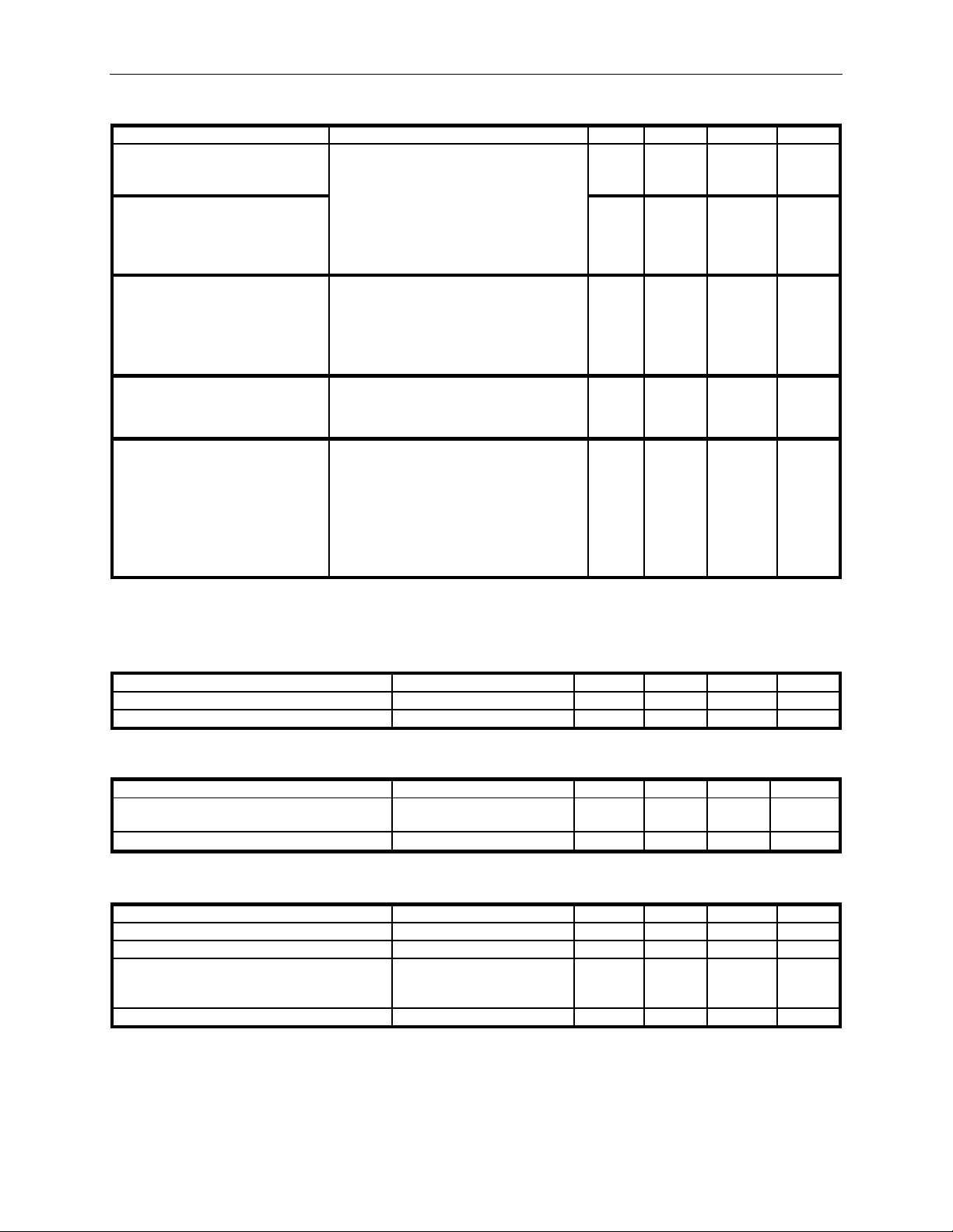
71M6521DE/DH/FE Data Sheet
PARAMETER
CONDITION
MIN
TYP
MAX
UNIT
Normal Operation,
ICE_E=0
Normal Operation as above, except write
PARAMETER
CONDITION
MIN
TYP
MAX
UNIT
On resistance – V3P3SYS to V3P3D
| I
V3P3D
| ≤ 1 mA
10
Ω
On resistance – VBAT to V3P3D
| I
V3P3D
| ≤ 1 mA
40
Ω
PARAMETER
CONDITION
MIN
TYP
MAX
UNIT
Reduce V3P3 until V2P5
drops 200mV
PSSR ∆V2P5/∆V3P3
RESET=0, iload=0
-3 +3
mV/V
PARAMETER
CONDITION
MIN
TYP
MAX
UNIT
V2P5
ILOAD=0
2.0
2.5
2.7
V
V2P5 load regulation
ILOAD=0 MA to 1 mA1 mA
30
mV
I
=1 MA,
REG_LP_OK=0
PSRR ΔV2P5/ΔVBAT
ILOAD=0
-50 50
mV/V
SUPPLY CURRENT
V3P3A + V3P3SYS current
V3P3A=V3P3SYS=3.3 V
6.1 7.7 mA
MPU_DIV=3 (614kHz) CKOUT_E=00,
CE_EN=1,
RTM_E=0,
VBAT current
ECK_DIS=1,
-300 +300 nA
ADC_E=1,
V3P3A + V3P3SYS current vs.
MPU clock frequency
V3P3A + V3P3SYS current,
write flash
VBAT current †
†
Current into V3P3A and V3P 3SYS pins is not zero if voltage is applied at thes e pins in brownout, LCD or sleep
modes.
1
Guaranteed by design; not production tested.
Same conditions as above 0.5
flash at maximum rate, CE_E=0,
9.1 10 mA
ADC_E=0
VBAT=3.6 V
BROWNOUT mode, <25°C
BROWNOUT mode, >25°C
LCD Mode, 25°C
LCD mode, over temperature
SLEEP Mode, 25°C
Sleep mode, over temperature
48
65
5.7
2.9
1
120
1501
8.5
15
5.0
101
1
mA/
MHz
µA
µA
µA
µA
µA
µA
V3P3D SWITCH
2.5 V VOLTAGE REGULATOR
Unless otherwise specified, lo ad = 5 mA
Voltage overhead V3P3-V2P5
440 mV
LOW POWER VOLTAGE REGULATOR
Unless otherwise specified, V3P3SYS=V3P3A=0, PB=GND (BROW NOUT)
LOAD
VBAT voltage requirement
Reduce VBAT until
3.0 V
Page: 92 of 107 Rev 2
Page 93
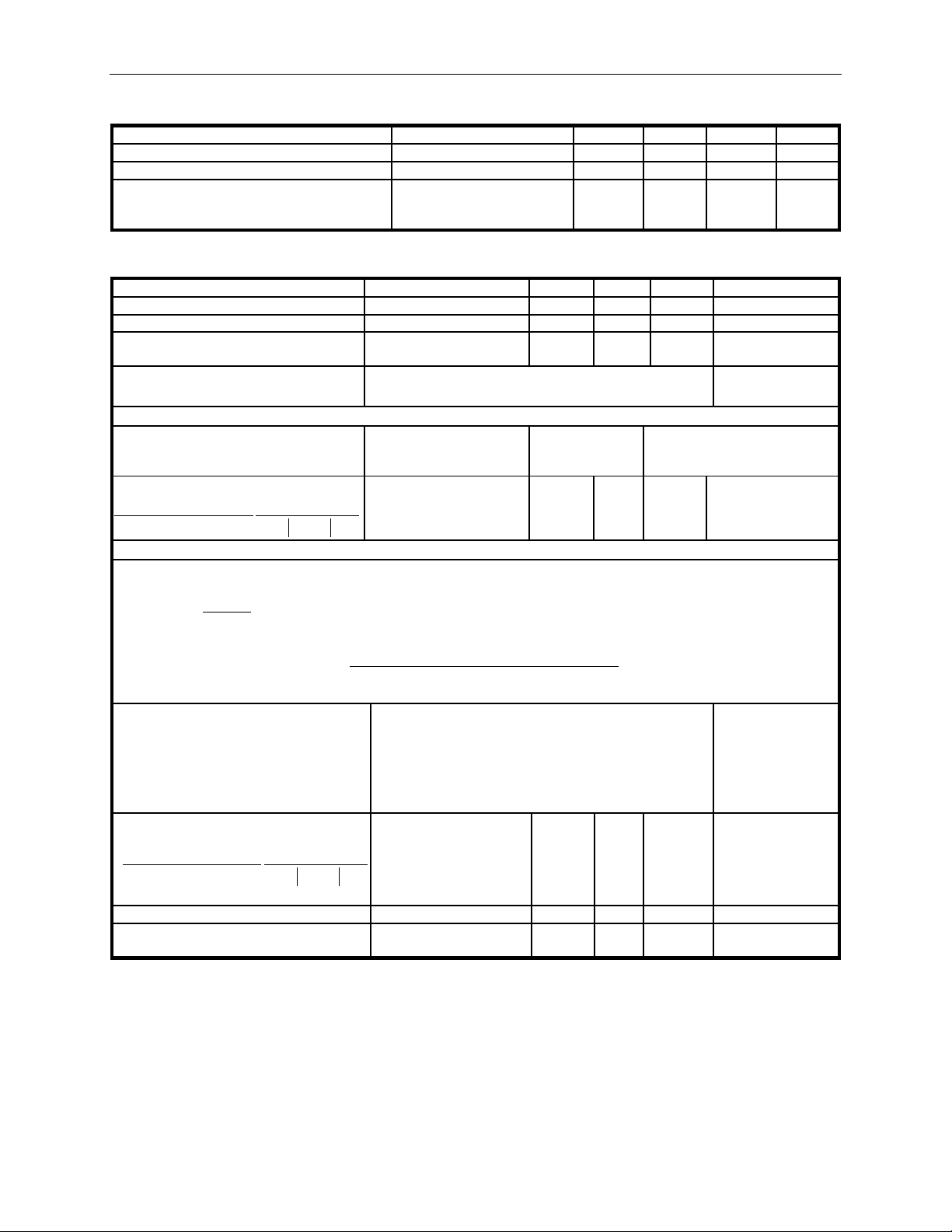
71M6521DE/DH/FE Data Sheet
PARAMETER
CONDITION
MIN
TYP
MAX
UNIT
Maximum Output Power to Crystal
Crystal connected
1
μW
XIN to XOUT Capacitance
3 pF
Capacitance to DGND
XOUT
5
pF
PARAMETER
CONDITION
MIN
TYP
MAX
UNIT
VREF output voltage, VNOM(25)
Ta = 22ºC
1.193
1.195
1.197
V
VREF chop step
50
mV
VREF_CAL =1,
ILOAD = 10 µA, -10 µA
2)22(1)22()22()(
2
TCTTCTVREFTVNOM −+−+=
-- If TRIMBGA and TRIMBGB not available --
VREF temperature coefficients
TC2
-0.341
µV/°C2
VREF(T) deviation from VNOM(T)
)40,22max(
10
)(
)()(
6
−−TTVNOM
TVNOMTVREF
-- If TRIMBGA and TRIMBGB are availabl e (71M6521DH) --
Define the following variables:
__/2
where TEMP_RAW_X is measured with FIRLEN=1
=
900
=(56.2
)
0.55
VNOM temperature coefficients
TC2
+ 19 0.065 + 0.34 + 8.0
0.015 0.0013 0.35
μV/ºC
)40,22max(
10
)(
)()(
6
−−TTVNOM
TVNOMTVREF
VREF aging
±25 ppm/ year
Ta = 25ºC
Ta = -40ºC to 85ºC
(-1%)
(-4%)1
1.6
1.61
(+1%)
(+4%)1 V V
CRYSTAL OSCILLATOR
XIN
VREF, VBIAS
Unless otherwise specified, VREF_DIS=0
VREF output impedance
VNOM definition2
TC1
--
,
,
=
.
,
--this calculates the value of TEMP22 if measured with FIRLEN=0
= 0.1 0.143 ( + 0.5
2.5 kΩ
Ta = -40ºC to +85ºC -401 +401 ppm/ºC
+7.0
5
V
µV/ºC
)
(500 + 370000
,
)
pF
(Δv and ΔT are defined in the
section entitled “Voltage Reference”)
TC1
VREF(T) deviation from VNOM(T)
VBIAS voltage
1
Guaranteed by design; not production tested.
2
This relationship describes the nominal behavior of VREF at different temperatures.
Rev 2 Page: 93 of 107
Ta = -40ºC to +85ºC -201 +201 ppm/ºC
μV/ºC
2
Page 94

71M6521DE/DH/FE Data Sheet
PARAMETER
CONDITION
MIN
TYP
MAX
UNIT
VLC2 Max Voltage
With respect to VLCD
-0.1 +0.1
V
VLC1 Voltage,
½ bias
With respect to VLC2/2
-3
+2
%
VLC0 Voltage,
½ bias
With respect to VLC2/2
-3
+2
%
PARAMETER
CONDITION
MIN
TYP
MAX
UNIT
Recommended Input Range
(Vin-V3P3A)
mV
peak
Voltage to Current Crosstalk:
)cos(
*10
6
VcrosstalkVin
Vin
Vcrosstalk
∠−∠
THD (First 10 harmonics)
20mV-pk
Vin=65 Hz,
Harris window
-90
dB
Input Impedance
Vin=65 Hz
40 90
kΩ
Temperature coefficient of Input
Impedance
FIR_LEN=0
FIR_LEN=1
357
151
FIR_LEN=0
FIR_LEN=1
+884736
±2097152
ADC Gain Error vs
3.3/33100
/35710
6
APV
VnVNout
INPK
∆
∆
Input Offset (Vin-V3P3A)
-10 10
mV
LCD DRIVERS
Applies to all COM and SEG pins.
1/3 bias
1/3 bias
With respect to 2*VLC2/3
With respect to VLC2/3
-4
-3
VLCD is V3P3SYS in MISSION mode and VBAT in BROWNOUT and LCD modes.
ADC CONVERTER, V3P3A REFERENCED
FIR_LEN=0, VREF_DIS=0, LSB values do not include the 9-bit left shift at CE input.
-250 250
Vin = 200 mV peak, 65
Hz, on VA
-101 101 μV/V
Vcrosstalk = largest
measurement on IA or IB
250mV-pk
64 kpts FFT, Blackman-
Vin=65 Hz 1.7 Ω/°C
LSB size
-75
0
+2
nV/LSB
%
%
dB
Digital Full Scale
%Power Supply Variation
1
Guaranteed by design; not production tested.
Vin=200 mV pk, 65 Hz
V3P3A=3.0 V, 3.6 V
LSB
50 ppm/%
Page: 94 of 107 Rev 2
Page 95

71M6521DE/DH/FE Data Sheet
PARAMETER
CONDITION
MIN
TYP
MAX
UNIT
Temperature Error†
+
−
−=
n
n
n
T
S
NTN
TERR
))((
TEMPERATURE SENSOR
A=25ºC, TA=75ºC,
Nominal Sensitivity (Sn) †
Nominal (Nn)
† †
1.0 106 LSB
1
Guaranteed by design; not production tested.
†
LSB values do not include the 9-bit left shif t at CE input.
††
Nn is measured at Tn during meter calibration and is stored in MPU or CE for use in temperature calculations.
T
FIR_LEN = 1
Nominal relationship:
N(T)= S
A = -40ºC to +85ºC
T
*(T-Tn)+Nn
n
Tn = 25°C
-2180 LSB/ºC
1
-10
+101 ºC
Rev 2 Page: 95 of 107
Page 96

71M6521DE/DH/FE Data Sheet
PARAMETER
CONDITION
MIN
TYP
MAX
UNIT
CKMPU = 4.9 MHz
5
Cycles
CKMPU = 1.25 MHz
2
Cycles
Flash write cycles
-40°C to +85°C
20,000
Cycles
Flash data retention
25°C
100
Years
Flash data retention
85°C
10
Years
Flash byte writes between page or mass
erase operations
PARAMETER
CONDITION
MIN
TYP
MAX
UNIT
Write Time per Byte
Page Erase (512 bytes)
Mass Erase
PARAMETER
CONDITION
MIN
TYP
MAX
UNIT
CKMPU=4.9 MHz, Using
interrupts
CKMPU=4.9 MHz, “bitbanging” DIO4/5
Write Clock frequency (3-wire)
PARAMETER
CONDITION
MIN
TYP
MAX
UNIT
Reset pulse fall time
11
µs
Reset pulse width
5 µs
PARAMETER
CONDITION
MIN
TYP
MAX
UNIT
Range for date
2000
-
2255
year
TIMING SPECIFICATIONS
RAM AND FLASH MEMORY
CE DRAM wait states
CKMPU = 614 kHz 1 Cycles
Flash Read Pulse Width
FLASH MEMORY TIMING
EEPROM INTERFACE
Write Clock frequency (I2C)
V3P3A=V3P3SYS=0
BROWNOUT MODE
2 Cycles
CKMPU=4.9 MHz
30
78 kHz
150 kHz
42 µs
20 ms
200 ms
500 kHz
100 ns
RESET and V1
1
Guaranteed by design; not production tested.
RTC
Page: 96 of 107 Rev 2
Page 97

71M6521DE/DH/FE Data Sheet
-0.5
-0.4
-0.3
-0.2
-0.1
0
0.1
0.2
0.3
0.4
0.5
0.1 1 10 100 1000
Current [A]
Error [%]
Phase_0
Phase_60
Phase_300
-8
-7
-6
-5
-4
-3
-2
-1
0
1
2
1 3 5 7 9 11 13 15 17 19 21 23 25
Harmonic
Error [ %]
50Hz Har monic Dat a 60Hz Harmonic Data
TYPICAL PERFORMANCE DATA
Rev 2 Page: 97 of 107
Figure 42: Wh Accuracy, 0.1A to 200A at 240V/50Hz and Room Temperature
Measured at current distortion amplitude of 40% and voltage distortion amplitude of 10%.
Figure 43: Meter Accuracy over Harmonics at 240V, 3 0A
Page 98

71M6521DE/DH/FE Data Sheet
11.7
12.3
0.60 Typ.
1.40
1.60
11.7
12.3
0.00
0.20
9.8
10.2
0.50 Typ.
0.14
0.28
PIN No. 1 Indicator
+
Relati ve A ccuracy over Temper at ure
-30
-20
-10
0
10
20
30
40
-60 -40 -20 0 20 40 60 80 100
Temp erature [°C]
Accuracy [PPM/°C]
Figure 44: Typical Meter Accuracy over Temperature Relative to 25°C (71M6521FE)
PACKAGE OUTLINE (LQFP 64)
Page: 98 of 107 Rev 2
NOTE: Controlling dimensions are in mm
PACKAGE OUTLINE (QFN 68)
Page 99

71M6521DE/DH/FE Data Sheet
Symbol
Min.
Nom.
Max.
Comment
Pin pitch (CC)
Pins per
column
Exposed pad
**)
Dimensions (in mm):
*) Pin length is nominally 0.4mm (min. 0.3mm, max 0.4mm)
**) Exposed pad is internally connected to GNDD.
e 0.4 BSC
Nd 17 Pins per row
Ne 17
A 0.85 0.90 Total height
A1 0.00 0.01 0.05
A2 0.65 0.70
A3 0.20 REF
b 0.15 0.20 0.25 Pin width *)
D 8.00 BSC Total width
D1 7.75 BSC
D2 6.3
E 8.00 BSC Total length
E1 7.75 BSC
E2 6.3 Exposed pad
b 0.15 0.20 0.25 Pad width
P 0.24 0.42 0.60 45° corner
θ
12° Angle
Rev 2 Page: 99 of 107
Page 100

71M6521DE/DH/FE Data Sheet
TERIDIAN
71M6521FE-IGT
GNDD
E_RXTX/SEG38
OPT_TX/DIO2
TMUXOUT
TX
SEG3
V3P3D
CKTEST/SEG19
V3P3SYS
SEG4
SEG5
SEG37/DIO17
COM1
COM0
COM2
33
64
RESET
V2P5
VBAT
RX
SEG31/DIO11
SEG30/DIO10
SEG29/DIO9
SEG28/DIO8
SEG27/DIO7
SEG26/DIO6
SEG25/DIO5
ICE_E
SEG24/DIO4
SEG18
SEG17
SEG16
COM3
SEG0
SEG35/DIO15
SEG36/DIO16
SEG6
SEG8
SEG1
SEG2
SEG34/DIO14
SEG7
SEG12
SEG10
SEG11
SEG9
SEG15
SEG13
SEG14
E_TCLK/SEG33
VA
OPT_RX/DIO1
TEST
GNDA
V3P3A
E_RST/SEG32
PB
XOUT
V1
XIN
X4MHZ
IA
VB
VREF
1
17
2
3
4
5
6
7
8
9
10
11
12
13
14
15
16
18
19
2021222423
25262728293031
32
34
35
36
37
38
39
40
41
42
43
44
45
46
47
48
63
62616059585756555453525150
49
IB
°
GNDD
E_RXTX/SEG38
1
2
3
4
5
6
7
8
9
10
11
12
13
14
15
16
17
68 67 66 65 64 63 62 61 60 59 58 57 56 55 54 53 52
18 19 20 21 22 23 24 25 26 27 28 29 30 31 32 33 34
51
50
49
48
47
46
45
44
43
42
41
40
39
38
37
36
35
OPT_TX/DIO2
TMUXOUT
DIO3
TX
SEG3
V3P3D
CKTEST/SEG19
V3P3SYS
SEG4
SEG5
SEG37/DIO17
COM0
COM1
COM2
COM3
SEG0
SEG1
SEG2
SEG34/DIO14
SEG35/DIO15
SEG36/DIO16
SEG39/DIO19
SEG6
SEG7
SEG8
SEG9
SEG10
SEG11
SEG12
SEG13
SEG14
SEG15
SEG16
SEG17
SEG18
ICE_E
SEG24/DIO4
SEG25/DIO5
SEG26/DIO6
SEG27/DIO7
SEG28/DIO8
SEG29/DIO9
SEG30/DIO10
SEG31/DIO11
SEG40/DIO20
RX
VBAT
V2P5
RESET
GNDA
V3P3A
VA
VB
IB
IA
VREF
V1
OPT_RX/DIO1
X4MHZ
XIN
XOUT
TEST
PB
E_RST/SEG32
E_TCLK/SEG33
SEG41/DIO21
TERIDIAN
PINOUT (LQFP-64)
PINOUT (QFN 68)
71M6521DE-IM
Page: 100 of 107 Rev 2
 Loading...