

Page 1
MAX4278
V
IN
75Ω
75Ω
V
OUT
75Ω
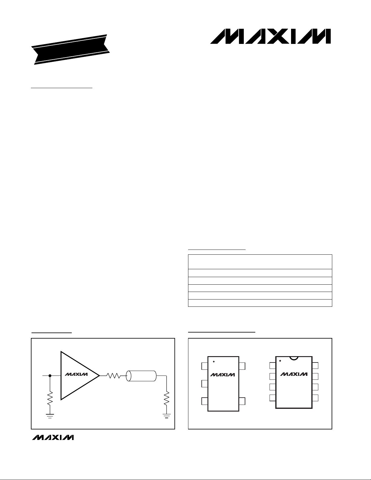
VIDEO/RF CABLE DRIVER
DIP/SO/µMAX
TOP VIEW
OUT
IN
N.C.
V
EE
1
2
8
7
N.C.
V
CC
GND
N.C.
MAX4178
MAX4278
3
4
6
5
V
EE
GNDIN
15V
CC
OUT
SOT23-5
2
34
MAX4178
MAX4278
19-0468; Rev 2; 11/99
General Description
The MAX4178/MAX4278 are ±5V, wide-bandwidth, fastsettling, closed-loop buffers featuring high slew rate, high
precision, high output current, low noise, and low differential gain and phase errors. The MAX4178, with a -3dB
bandwidth of 330MHz, is preset for unity voltage gain
(0dB). The MAX4278 is preset for a voltage gain of +2
(6dB) and has a 310MHz -3dB bandwidth.
The MAX4178/MAX4278 feature the high slew rate and
low power that are characteristic of current-mode feedback amplifiers. However, unlike conventional currentmode feedback amplifiers, these devices have a
unique input stage that combines the benefits of current-feedback topology with those of the traditional voltage-feedback topology. This combination results in low
input offset voltage and bias current, low noise, and
high gain precision and power-supply rejection.
The MAX4178/MAX4278 are ideally suited for driving
50Ω or 75Ω loads. They are the perfect choice for highspeed cable-driving applications, such as video routing.
The MAX4178/MAX4278 are available in DIP, SO,
space-saving µMAX, and SOT23 packages.
________________________Applications
Broadcast and High-Definition TV Systems
Video Switching and Routing
High-Speed Cable Drivers
Communications
Medical Imaging
Precision High-Speed DAC/ADC Buffers
____________________________Features
♦ High Speed
330MHz -3dB Bandwidth (MAX4178)
310MHz -3dB Bandwidth (MAX4278)
250MHz Full-Power Bandwidth (V
OUT
= 2Vp-p)
150MHz 0.1dB Flatness Bandwidth
1300V/µs Slew Rate (MAX4178)
1600V/µs Slew Rate (MAX4278)
♦ Low Differential Phase/Gain Error: 0.01°/0.04%
♦ 8mA Supply Current
♦ 1µA Input Bias Current
♦ 0.5mV Input Offset Voltage
♦ 5nV/
√
HHzz
Input-Referred Voltage Noise
♦ 2pA/
√
HHzz
Input-Referred Current Noise
♦ 1.0% Max Gain Error with 100Ω Load
♦ Short-Circuit Protected
♦ 8000V ESD Protection
♦ Available in Space-Saving SOT23 Package
MAX4178/MAX4278
330MHz, Gain of +1/Gain of +2
Closed-Loop Buffers
________________________________________________________________ Maxim Integrated Products 1
For pricing, delivery, and ordering information, please contact Maxim/Dallas Direct! at
1-888-629-4642, or visit Maxim’s website at www.maxim-ic.com.
PART
MAX4178EPA
MAX4178ESA
MAX4178EUA -40°C to +85°C
-40°C to +85°C
-40°C to +85°C
TEMP. RANGE
PINPACKAGE
8 Plastic DIP
8 SO
8 µMAX
EVALUATION KIT
AVAILABLE
Ordering Information
Ordering Information continued at end of data sheet.
Pin Configurations
Typical Operating Circuit
MAX4178MJA -55°C to +125°C 8 CERDIP
MAX4178EUK-T -40°C to +85°C 5 SOT23-5
SOT
TOP MARK
—
—
—
—
ABYX
Page 2
MAX4178/MAX4278
330MHz, Gain of +1/Gain of +2
Closed-Loop Buffers
2 ______________________________________________________________________________________
ABSOLUTE MAXIMUM RATINGS
DC ELECTRICAL CHARACTERISTICS
(VCC= +5V, VEE= -5V, V
OUT
= 0, RL= ∞, TA= T
MIN
to T
MAX
, unless otherwise noted. Typical values are at TA= +25°C.)
Stresses beyond those listed under “Absolute Maximum Ratings” may cause permanent damage to the device. These are stress ratings only, and functional
operation of the device at these or any other conditions beyond those indicated in the operational sections of the specifications is not implied. Exposure to
absolute maximum rating conditions for extended periods may affect device reliability.
Supply Voltage (VCCto VEE)..................................................12V
Input Voltage....................................(V
CC
+ 0.3V) to (VEE- 0.3V)
Output Short-Circuit Duration (to GND) .....................Continuous
Continuous Power Dissipation (T
A
= +70°C)
SOT23 (derate 7.10mW/°C above +70°C)..................571mW
Plastic DIP (derate 9.09mW/°C above +70°C) ...........727mW
SO (derate 5.88mW/°C above +70°C)........................471mW
µMAX (derate 4.10mW/°C above +70°C) ...................330mW
CERDIP (derate 8.00mW/°C above +70°C)................640mW
Operating Temperature Ranges (Note 1)
MAX4178E_A/MAX4278E_A...........................-40°C to +85°C
MAX4178EUK/MAX4278EUK .........................-40°C to +85°C
MAX4178MJA/MAX4278MJA .......................-55°C to +125°C
Storage Temperature Range .............................-65°C to +160°C
Lead Temperature (soldering, 10s) .................................+300°C
CONDITIONS
UNITSMIN TYP MAXSYMBOLPARAMETER
MAX4178 ±2.5 ±3.0
MAX4278
V
±1.25 ±1.5
V
IN
Input Voltage Range
0.5 2.0
µV/°C2TCV
OS
Input Offset Voltage Drift
13
µAI
B
Input Bias Current
MΩ1R
IN
Input Resistance
VS= ±4.5V to ±5.5V dB70 90PSRR
Power-Supply Rejection
Ratio
+0.990 +1.000
MAX4178 (Note 2)
+0.985 +1.000
+1.98 +2.01
MAX4278 (Note 3)
V/V
+1.97 +2.01
A
V
Voltage Gain
V
OUT
= ±1mV to ±2V %0.01A
V(LIN)
Gain Linearity
f = DC Ω0.1R
OUT
Output Resistance
Short to GND mA150I
SC
Short-Circuit Output Current
RL= 100Ω ±2.5 ±3.0
TA = +25°C
RL= 100Ω
RL= 50Ω
RL= 100Ω
RL= 50Ω
RL= 50Ω
V
±2.0 ±2.5
V
OUT
Output Voltage Swing
TA= +25°C 810
12
mA
14
TA = T
MIN
to T
MAX
I
SY
Quiescent Supply Current
MAX4_78E_ _
MAX4_78MJA
TA = -40°C to +85°C mA70 100I
OUT
Minimum Output Current
3.0
TA = T
MIN
to T
MAX
5
Note 2: Voltage Gain = (V
OUT
- VOS) / VINmeasured at VIN= ±2.5V.
Note 3: Voltage Gain = (V
OUT
- VOS) / VINmeasured at VIN= ±1.25V.
TA = +25°C
0.5 3.0
TA =
T
MIN
to T
MAX
5.0
mVV
OS
Input Offset Voltage
MAX4_78ESA/EPA/EUA/MJA
MAX4_78EUK
MAX4_78ESA/EPA/EUA/MJA
MAX4_78EUK
Note 1: Specifications for the MAX4_78EUK (SOT23 packages) are 100% tested at TA= +25°C, and guaranteed by design over
temperature.
Page 3
MAX4178/MAX4278
330MHz, Gain of +1/Gain of +2
Closed-Loop Buffers
________________________________________________________________________________________ 3
AC ELECTRICAL CHARACTERISTICS
(VCC= +5V, VEE= -5V, RL= 100Ω, TA= +25°C, unless otherwise noted.)
Note 4: Tested with a 3.58MHz video test signal with an amplitude of 40IRE superimposed on a linear ramp (0 to 100IRE). An IRE is
a unit of video signal amplitude developed by the Institute of Radio Engineers; 140IRE = 1V in color systems.
CONDITIONS
V
OUT
= 2V step ns2tR, t
F
Rise/Fall Times
f = 10MHz nV/√Hz5e
n
Input Voltage Noise Density
f = 10MHz pA/√Hz2i
n
Input Current Noise Density
0.04
f = 3.58MHz %
0.04
DG
Differential Gain
(Note 4)
f = 5MHz, V
OUT
= 2Vp-p dBC
-81
SFDRSpurious-Free Dynamic Range
36
fC= 10MHz,
V
OUT
= 2Vp-p
dBm
31
IP3Third-Order Intercept
UNITSMIN TYP MAXPARAMETER
MAX4278
330
V
OUT
≤ 0.1Vp-p MHz
310
BWSmall-Signal, -3dB Bandwidth
MAX4178
to 0.01%
10
V
OUT
= 2V step ns
12
t
S
Settling Time
to 0.1%
MAX4178
MAX4278
0.01
MAX4278
MAX4178
f = 3.58MHz degrees
0.01
DP
Differential Phase
(Note 4)
-58
MAX4278
MAX4178
fC= 10MHz,
V
OUT
= 2Vp-p
dB
-59
THDTotal Harmonic Distortion
MAX4178
MAX4278
pF1C
IN
Input Capacitance
MAX4178
MAX4278 -74
SYMBOL
150MAX4178
150MAX4278
MHzV
OUT
≤ 0.1Vp-pBW
(0.1dB)
Small-Signal, ±0.1dB Bandwidth
1600
1300MAX4178
MAX4278
250
V
OUT
= 2Vp-p
V/µs
MHz
250
FPBW
V
OUT
= ±2Vp-p
MAX4278
Full-Power Bandwidth
MAX4178
SRSlew Rate
Page 4
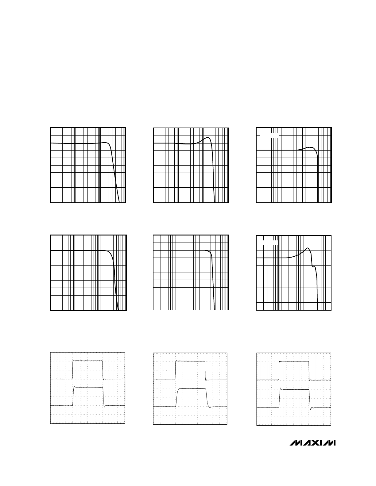
__________________________________________Typical Operating Characteristics
(VCC= +5V, VEE= -5V, RL= 100Ω, CL= 0pF, TA = +25°C, unless otherwise noted.)
MAX4178/MAX4278
330MHz, Gain of +1/Gain of +2
Closed-Loop Buffers
4 ______________________________________________________________________________________
SMALL-SIGNAL GAIN vs. FREQUENCY
MAX4178
2
1
1G
MAX4178/4278-01
GAIN (dB)
-0.1
-0.2
-0.3
-0.4
-0.5
-0.6
-0.7
-0.8
0
-1
-2
-3
GAIN (dB)
-4
-5
-6
-7
-8
1M
10M
FREQUENCY (Hz)
100M
MAX4278
SMALL-SIGNAL GAIN vs. FREQUENCY
8
7
6
5
4
3
GAIN (dB)
2
1
0
-1
-2
1M
10M
FREQUENCY (Hz)
100M
MAX4178/4278-04
GAIN (dB)
1G
GAIN FLATNESS vs. FREQUENCY
MAX4178
0.2
0.1
0
1M
10M
FREQUENCY (Hz)
MAX4278
GAIN FLATNESS vs. FREQUENCY
6.2
6.1
6.0
5.9
5.8
5.7
5.6
5.5
5.4
5.3
5.2
1M
10M
FREQUENCY (Hz)
100M
100M
MAX4178/4278-02
1G
MAX4178/4278-05
1G
LARGE-SIGNAL GAIN vs. FREQUENCY
MAX4178
3
VO = 2Vp-p
2
1
0
-1
-2
GAIN (dB)
-3
-4
-5
-6
-7
1M
10M
FREQUENCY (Hz)
MAX4278
LARGE-SIGNAL GAIN vs. FREQUENCY
12
VO = 2Vp-p
10
8
6
4
2
GAIN (dB)
0
-2
-4
-6
-8
1M
10M
FREQUENCY (Hz)
100M
100M
MAX4178/4278-03
1G
MAX4178/4278-06
1G
PULSE RESPONSE (C
IN
OUT
VOLTAGE (100mV/div)
MAX4178
SMALL-SIGNAL
TIME (10ns/div)
= 0pF)
L
MAX4178/4278-07
GND
GND
IN
OUT
VOLTAGE (2V/div)
MAX4178
LARGE-SIGNAL
PULSE RESPONSE (C
TIME (10ns/div)
= 0pF)
L
MAX4178/4278-08
GND
GND
(50mV/
div)
VOLTAGE
OUT
(100mV/
div)
SMALL-SIGNAL
PULSE RESPONSE (C
IN
TIME (10ns/div)
MAX4278
= 0pF)
L
MAX4178/4278-09
GND
GND
Page 5

Typical Operating Characteristics (continued)
(VCC= +5V, VEE= -5V, RL= 100Ω, CL= 0pF, TA = +25°C, unless otherwise noted.)
MAX4178/MAX4278
330MHz, Gain of +1/Gain of +2
Closed-Loop Buffers
_______________________________________________________________________________________ 5
(1V/div)
VOLTAGE
OUT
(2V/div)
IN
PULSE RESPONSE (C
IN
PULSE RESPONSE (C
MAX4278
LARGE-SIGNAL
TIME (10ns/div)
MAX4178
SMALL-SIGNAL
L
= 0pF)
L
= 100pF)
MAX4178/4278-10
GND
GND
VOLTAGE (100mV/div)
MAX4178/4278-13
GND
PULSE RESPONSE (C
IN
OUT
PULSE RESPONSE (C
IN
MAX4178
SMALL-SIGNAL
TIME (20ns/div)
MAX4178
LARGE-SIGNAL
= 50pF)
L
= 100pF)
L
MAX4178/4278-11
GND
GND
MAX4178/4278-14
GND
PULSE RESPONSE (C
IN
OUT
VOLTAGE (2V/div)
PULSE RESPONSE (C
IN
(50mV/
div)
MAX4178
LARGE-SIGNAL
TIME (20ns/div)
MAX4278
SMALL-SIGNAL
= 50pF)
L
= 50pF)
L
MAX4178/4278-12
GND
GND
MAX4178/4278-15
GND
OUT
VOLTAGE (100mV/div)
PULSE RESPONSE (C
IN
(1V/div)
VOLTAGE
OUT
(2V/div)
VOLTAGE
OUT
(100mV/
GND
MAX4178/4278-17
GND
GND
div)
IN
(1V/div)
VOLTAGE
OUT
(2V/div)
TIME (20ns/div)
MAX4278
LARGE-SIGNAL
PULSE RESPONSE (C
TIME (20ns/div)
= 100pF)
L
TIME (20ns/div)
MAX4278
LARGE-SIGNAL
TIME (20ns/div)
= 50pF)
L
GND
MAX4178/4278-16
GND
GND
OUT
VOLTAGE (2V/div)
IN
(50mV/
div)
VOLTAGE
OUT
(100mV/
div)
TIME (20ns/div)
MAX4278
SMALL-SIGNAL
PULSE RESPONSE (C
TIME (20ns/div)
= 100pF)
L
GND
MAX4178/4278-18
GND
GND
Page 6

Typical Operating Characteristics (continued)
(VCC= +5V, VEE= -5V, RL= 100Ω, CL= 0pF, TA = +25°C, unless otherwise noted.)
MAX4178/MAX4278
330MHz, Gain of +1/Gain of +2
Closed-Loop Buffers
6 ______________________________________________________________________________________
MAX4178
DIFFERENTIAL PHASE/GAIN
0.02
0.00
-0.02
-0.04
DIFF GAIN (%)
-0.002
-0.004
-0.006
-0.008
DIFF PHASE (deg)
-0.010
= 150Ω
R
L
-0.06
0
0.002
0.000
RL = 150Ω
0 100
IRE
IRE
MAX4278
MAX4178/4278-19
DIFF GAIN (%)
100
DIFF PHASE (deg)
HARMONIC DISTORTION
vs. FREQUENCY
-40
-50
TOTAL HARMONIC DISTORTION
-60
-70
-80
DISTORTION (dB)
-90
-100
10k 1M 10M100k 100M
SECOND HARMONIC
THIRD HARMONIC
FREQUENCY (Hz)
MAX4178/4278-22
POWER-SUPPLY REJECTION (dB)
-100
-110
0.02
0.01
0.00
-0.01
-0.02
-0.03
-0.04
= 150Ω
R
L
-0.05
-0.06
0
0.002
0.000
-0.002
-0.004
RL = 150Ω
-0.006
0 100
-20
-30
-40
-50
-60
-70
-80
MAX4278
-90
MAX4178
30k 100k 1M 10M 100M
MAX4278
DIFFERENTIAL PHASE/GAIN
IRE
IRE
POWER-SUPPLY REJECTION
vs. FREQUENCY
FREQUENCY (Hz)
100
-20
MAX4178/4278-20
-40
-60
DISTORTION (dB)
-80
-100
1k
MAX4178/4278-23
100
10
OUTPUT IMPEDANCE (Ω)
0.1
MAX4178
HARMONIC DISTORTION
vs. FREQUENCY
MAX4178/4278-21
TOTAL HARMONIC DISTORTION
SECOND HARMONIC
THIRD HARMONIC
1k 10k 1M 10M100k 100M
FREQUENCY (Hz)
OUTPUT IMPEDANCE
vs. FREQUENCY
MAX4178/4278-24
1
MAX4278
MAX4178
100k 1M 10M 100M 500M
FREQUENCY (Hz)
INPUT OFFSET VOLTAGE (VOS)
vs. TEMPERATURE
400
VIN = 0V
300
200
100
0
-100
INPUT OFFSET VOLTAGE (µV)
-200
-300
-50
-25 0 25 50 75 125100
TEMPERATURE (˚C)
MAX4178/4278-25
QUIESCENT SUPPLY CURRENT (ISY)
vs. TEMPERATURE
14
12
10
8
6
4
2
QUIESCENT SUPPLY CURRENT (mA)
0
-25 0 25 50 75 125100
-50
TEMPERATURE (˚C)
3.5
V
3.0
MAX4178/4278-26
2.5
2.0
1.5
1.0
INPUT BIAS CURRENT (µA)
0.5
0
-50
INPUT BIAS CURRENT (IB)
vs. TEMPERATURE
= 0V
IN
-25 0 25 50 75 125100
TEMPERATURE (˚C)
MAX4178/4278-27
Page 7
MAX4178/MAX4278
330MHz, Gain of +1/Gain of +2
Closed-Loop Buffers
________________________________________________________________________________________ 7
Detailed Description
The MAX4178/MAX4278 are ±5V, wide-bandwidth,
fast-settling, closed-loop buffers featuring high slew
rate, high precision, high output current, low noise, and
low differential gain and phase errors. The MAX4178,
with a -3dB bandwidth of 330MHz, is preset for unity voltage gain (0dB). The MAX4278 is preset for a voltage gain
of +2 (6dB) and has a 310MHz -3dB bandwidth.
These devices have a unique input stage that combines the benefits of a current-mode-feedback topology (high slew rate and low power) with those of a
traditional voltage-feedback topology. This combination
of architectures results in low input offset voltage and
bias current, and high gain precision and power-supply
rejection.
Under short-circuit conditions, the output current is typically limited to 150mA. This is low enough that a short
to ground of any duration will not cause permanent
damage to the chip. However, a short to either supply
will create double the allowable power dissipation and
may cause permanent damage if allowed to exist for
longer than approximately 10 seconds. The high output-current capability is an advantage in systems that
transmit a signal to several loads. See the High-
Performance Video Distribution Amplifier section.
Typical Operating Characteristics (continued)
(VCC= +5V, VEE= -5V, RL= 100Ω, CL= 0pF, TA = +25°C, unless otherwise noted.)
Pin Description
1
5
2
3
4
—
Output6
Positive Power Supply.
Connect to +5V.
7
Negative Power Supply.
Connect to -5V.
4
Input3
Ground2
No Connection1, 5, 8
PIN
OUT
V
CC
V
EE
IN
GND
N.C.
NAME
SOT23SO/µMAX/DIP
FUNCTION
OUTPUT VOLTAGE SWING
vs. TEMPERATURE
8
4.0
3.5
3.0
OUTPUT VOLTAGE SWING (±V)
2.5
-25 0 25 50 75 125100
-50
TEMPERATURE (˚C)
RL =
MAX4178/4278-28
RL = 100Ω
RL = 50Ω
INPUT VOLTAGE RANGE
4.5
4.0
3.5
3.0
2.5
2.0
INPUT VOLTAGE RANGE (±V)
1.5
1.0
-50
vs. TEMPERATURE
-25 0 25 50 75 125100
TEMPERATURE (˚C)
MAX4178/4278-29
MAX4178
MAX4278
Page 8

MAX4178/MAX4278
330MHz, Gain of +1/Gain of +2
Closed-Loop Buffers
8 ______________________________________________________________________________________
Applications Information
Grounding, Bypassing,
and PC Board Layout
In order to obtain the MAX4178/MAX4278s’ full 330MHz/
310MHz bandwidths, microstrip and stripline techniques are recommended in most cases. To ensure
that the PC board does not degrade the amplifier’s performance, it’s a good idea to design the board for a frequency greater than 1GHz. Even with very short traces,
it’s good practice to use these techniques at critical
points, such as inputs and outputs. Whether you use a
constant-impedance board or not, observe the following guidelines when designing the board:
• Do not use wire-wrap boards. They are too inductive.
• Do not use IC sockets. They increase parasitic capaci-
tance and inductance.
• In general, surface-mount components have shorter
leads and lower parasitic reactance, giving better
high-frequency performance than through-hole components.
• The PC board should have at least two layers, with
one side a signal layer and the other a ground plane.
• Keep signal lines as short and straight as possible.
Do not make 90° turns; round all corners.
• The ground plane should be as free from voids as
possible.
On Maxim’s evaluation kit, the ground plane has been
removed from areas where keeping the trace capacitance to a minimum is more important than maintaining
ground continuity.
Driving Capacitive Loads
The MAX4178/MAX4278 provide maximum AC performance with no output load capacitance. This is the
case when the MAX4178/MAX4278 are driving a correctly terminated transmission line (e.g., a back-terminated 75Ω cable). However, the MAX4178/MAX4278
are capable of driving capacitive loads up to 100pF
without oscillations, but with reduced AC performance.
Driving large capacitive loads increases the chance of
oscillations in most amplifier circuits. This is especially
true for circuits with high loop gains, such as voltage
followers. The amplifier’s output resistance and the load
capacitor combine to add a pole and excess phase to
the loop response. If the frequency of this pole is low
enough and if phase margin is degraded sufficiently,
oscillations may occur.
A second problem when driving capacitive loads
results from the amplifier’s output impedance, which
looks inductive at high frequency. This inductance
forms an L-C resonant circuit with the capacitive load,
which causes peaking in the frequency response and
degrades the amplifier’s gain margin.
The MAX4178/MAX4278 drive capacitive loads up to
100pF without oscillation. However, some peaking (in
the frequency domain) or ringing (in the time domain)
may occur. This is shown in Figures 2a and 2b and the
in the Small- and Large-Signal Pulse Response graphs
in the Typical Operating Characteristics.
To drive larger-capacitance loads or to reduce ringing,
add an isolation resistor between the amplifier’s output
and the load, as shown in Figure 1.
The value of R
ISO
depends on the circuit’s gain and the
capacitive load. Figures 3a and 3b show the Bode
plots that result when a 20Ω isolation resistor is used
with a voltage follower driving a range of capacitive
loads. At the higher capacitor values, the bandwidth is
dominated by the RC network, formed by R
ISO
and CL;
the bandwidth of the amplifier itself is much higher.
Note that adding an isolation resistor degrades gain
accuracy. The load and isolation resistor form a divider
that decreases the voltage delivered to the load.
Figure 1. Capacitive-Load Driving Circuit
R
V
IN
MAX4178
MAX4278
ISO
C
L
V
OUT
R
L
Page 9

MAX4178/MAX4278
330MHz, Gain of +1/Gain of +2
Closed-Loop Buffers
________________________________________________________________________________________ 9
Figure 3b. MAX4278 Small-Signal Gain vs. Frequency with
Capacitive Load and Isolation Resistor (R
ISO
)
Figure 2a. MAX4178 Small-Signal Gain vs. Frequency with
Capacitive Load
MAX4278 SMALL SIGNAL GAIN vs.
Figure 2b. MAX4278 Small-Signal Gain vs. Frequency with
Capacitive Load
Figure 3a. MAX4178 Small-Signal Gain vs. Frequency with
Capacitive Load and Isolation Resistor (R
ISO
)
FREQUENCY WITH CAPACITIVE LOAD
20
R
= 0Ω CL = 100pF
ISO
15
10
5
0
-5
GAIN (dB)
-10
-15
-20
-25
-30
1M 100M 1G
10M
FREQUENCY (Hz)
CL = 0pF
CL = 47pF
CL = 22pF
MAX4178/4278-2a
AND ISOLATION RESISTOR
2
R
= 20Ω
ISO
1
0
-1
-2
-3
GAIN (dB)
-4
-5
-6
-7
-8
CL = 47pF
CL = 100pF
1M 100M 1G
CL = 22pF
CL = 0pF
MAX4178/4278-3a
10M
FREQUENCY (Hz)
FREQUENCY WITH CAPACITIVE LOAD
26
R
= 0Ω CL = 100pF
ISO
21
16
11
6
1
GAIN (dB)
-4
-9
-14
-19
-24
1M 100M 1G
10M
FREQUENCY (Hz)
CL = 0pF
CL = 47pF
CL = 22pF
MAX4178/4278-2b
AND ISOLATION RESISTOR
8
R
= 20Ω
ISO
7
6
5
4
3
GAIN (dB)
2
1
0
-1
-2
CL = 47pF
CL = 100pF
1M 100M 1G
CL = 22pF
CL = 0pF
MAX4178/4278-3b
10M
FREQUENCY (Hz)
Page 10

MAX4178/MAX4278
330MHz, Gain of +1/Gain of +2
Closed-Loop Buffers
10 _____________________________________________________________________________________
Flash ADC Preamp
The MAX4178/MAX4278s’ high current-drive capability
makes them well suited for buffering the low-impedance input of a high-speed flash ADC. With their low
output impedance, these buffers can drive the inputs of
the ADC with no loss of accuracy. Figure 4 shows a
preamp for digitizing video, using the 250Msps
MAX100 and the 500Msps MAX101 flash ADCs. Both of
these ADCs have a 50Ω input resistance and a 1.2GHz
input bandwidth.
High-Performance
Video Distribution Amplifier
The MAX4278 (AV= +2) makes an excellent driver for
multiple back-terminated 75Ω video coaxial cables
(Figure 5). The high current-output capability allows the
attachment of up to six ±2Vp-p, 150Ω loads to the
MAX4278 at +25°C. With the output limited to ±1Vp-p,
the number of loads may double. For multiple gain-of-2
video line drivers in a single package, refer to the
MAX496/MAX497data sheet.
Figure 4. Preamp for Video Digitizer
Figure 5. High-Performance Video Distribution Amplifier
___________________Chip Information
TRANSISTOR COUNT: 175
SUBSTRATE CONNECTED TO V
EE
Ordering Information (continued)
PART
MAX4278EPA
MAX4278ESA
MAX4278EUA -40°C to +85°C
-40°C to +85°C
-40°C to +85°C
TEMP. RANGE
PINPACKAGE
8 Plastic DIP
8 SO
8 µMAX
MAX4278MJA -55°C to +125°C 8 CERDIP
MAX4278EUK-T -40°C to +85°C 5 SOT23-5
SOT
TOP MARK
–
–
–
–
ABYY
VIDEO IN
MAX4178
MAX4278
FLASH ADC
(MAX100/MAX101)
75Ω
VIDEO IN
MAX4278
75Ω
75Ω
75Ω
OUT1
75Ω
75Ω
OUT2
75Ω
75Ω
OUTN
75Ω
Page 11

MAX4178/MAX4278
330MHz, Gain of +1/Gain of +2
Closed-Loop Buffers
_______________________________________________________________________________________ 11
Package Information
(The package drawing(s) in this data sheet may not reflect the most current specifications. For the latest package outline information
go to www.maxim-ic.com/packages.)
PDIPN.EPS
N
1
e
TOP VIEW
D
FRONT VIEW
INCHES
DIM
MIN
0.053A
0.004
A1
0.014
B
0.007
C
e 0.050 BSC 1.27 BSC
0.150
HE
A
B
A1
C
L
E
H 0.2440.228 5.80 6.20
0.016L
VARIATIONS:
INCHES
MINDIM
D
0.189 0.197 AA5.004.80 8
0.337 0.344 AB8.758.55 14
D
0∞-8∞
SIDE VIEW
PROPRIETARY INFORMATION
TITLE:
PACKAGE OUTLINE, .150" SOIC
MAX
0.069
0.010
0.019
0.010
0.157
0.050
MAX
0.3940.386D
MILLIMETERS
MIN
1.35
1.75
0.10
0.25
0.35
0.49
0.19
0.25
3.80 4.00
0.40 1.27
MILLIMETERS
MAX
MIN
9.80 10.00
21-0041
MAX
N MS012
16
REV.DOCUMENT CONTROL NO.APPROVAL
SOICN .EPS
AC
1
B
1
Page 12
MAX4178/MAX4278
330MHz, Gain of +1/Gain of +2
Closed-Loop Buffers
___________________________________________Package Information (continued)
Maxim cannot assume responsibility for use of any circuitry other than circuitry entirely embodied in a Maxim product. No circuit patent licenses are
implied. Maxim reserves the right to change the circuitry and specifications without notice at any time.
12 ____________________Maxim Integrated Products, 120 San Gabriel Drive, Sunnyvale, CA 94086 408-737-7600
© 1999 Maxim Integrated Products Printed USA is a registered trademark of Maxim Integrated Products.
(The package drawing(s) in this data sheet may not reflect the most current specifications. For the latest package outline information
go to www.maxim-ic.com/packages.)
8
ÿ 0.50±0.1
0.6±0.1
1
0.6±0.1
A2
D
TOP VIEW
e
FRONT VIEW
E H
A1
A
c
b
4X S
L
BOTTOM VIEW
SIDE VIEW
8
1
DIM
A
A1
A2
b
c
D
e
E
H
L
α
S
INCHES
MIN
-
0.002
0.030
0.010
0.005
0.116
0.0256 BSC
0.116
0.188
0.016
0∞
0.0207 BSC
MAX
0.043
0.006
0.037
0.014
0.007
0.120
0.120
0.198
0.026
6∞
MILLIMETERS
MAX
MIN
- 1.10
0.05 0.15
0.950.75
0.25 0.36
0.13 0.18
2.95 3.05
0.65 BSC
2.95 3.05
4.78
5.03
0.41
0.66
0.5250 BSC
8LUMAXD.EPS
6∞0∞
α
PROPRIETARY INFORMATION
TITLE:
PACKAGE OUTLINE, 8L uMAX/uSOP
21-0036
REV.DOCUMENT CONTROL NO.APPROVAL
1
J
1
SOT5L.EPS
 Loading...