

Page 1
General Description
The MAX11800–MAX11803 low-power touch-screen controllers operate from a single supply of 1.70V to 3.6V, targeting power-sensitive applications such as handheld
equipment. The devices contain a 12-bit SAR ADC and a
multiplexer to interface with a resistive touch-screen
panel. A digital serial interface provides communications.
The MAX11800–MAX11803 include digital preprocessing
of the touch-screen measurements, reducing bus loading
and application-processor resource requirements. The
included smart interrupt function generator greatly
reduces the frequency of interrupt servicing to the
devices. The MAX11800–MAX11803 enter low-power
modes automatically between conversions to save power,
making the devices ideal for portable applications.
The MAX11800/MAX11801 offer two modes of operation:
direct and autonomous. Direct mode allows the application processor to control all touch-screen controller activity. Autonomous mode allows the MAX11800/MAX11801
to control touch-screen activity, thereby freeing the
application processor to perform other functions. In
autonomous mode, the devices periodically scan the
touch screen for touch events without requiring hostprocessor intervention. This can be used to reduce system power consumption. An on-chip FIFO is used during
autonomous mode to store results, increasing effective
data throughput and lower system power.
The MAX11800–MAX11803 support data-tagging,
which records the type of measurement performed; X,
Y, Z1, or Z2, and the type of touch event; initial touch,
continuing touch, or touch release.
The MAX11800/MAX11802 support the SPI™ serial bus.
The MAX11801/MAX11803 support the I2C serial bus.
The MAX11800–MAX11803 are available in 12-pin TQFN
and 12-pin WLP packages, and are specified over the
-40°C to +85°C (extended) and -40°C to +105°C (automotive) temperature ranges.
Applications
Features
♦ 4-Wire Touch-Screen Interface
♦ X/Y Coordinate and Touch Pressure Measurement
♦ Ratiometric Measurement
♦ 12-Bit SAR ADC
♦ Single 1.7V to 3.6V Supply
♦ Two Operating Modes—Direct and Autonomous
♦ Data Tagging Provides Measurement and Touch
Event Information
♦ Data Filtering Provides Noise Reduction
♦ Aperture Mode Provides Spatial Filtering
♦ Digital Processing Reduces Bus Activity and
Interrupt Generation
♦ Programmable Touch-Detect Pullup Resistors
♦ Auto Power-Down Control for Low-Power
Operation
♦ 25MHz SPI Interface (MAX11800/MAX11802)
♦ 400kHz I
2
C Interface (MAX11801/MAX11803)
♦ 1.6mm x 2.1mm, 12-Pin WLP and 4mm x 4mm,
12-Pin TQFN
♦ Low-Power Operation
343µW at VDD= 1.7V, 34.4ksps
888µW at VDD= 3.3V, 34.4ksps
♦ ESD Protection
±4kV HBM
±8kV HBM (X+, X-, Y+, Y-)
±1kV CDM
±200V MM
MAX11800–MAX11803
Low-Power, Ultra-Small Resistive
Touch-Screen Controllers with I2C/SPI Interface
________________________________________________________________
Maxim Integrated Products
1
Ordering Information
19-4711; Rev 3; 10/10
For pricing, delivery, and ordering information, please contact Maxim Direct at 1-888-629-4642,
or visit Maxim’s website at www.maxim-ic.com.
EVALUATION KIT
AVAILABLE
PART TEMP RANGE PIN-PACKAGE
MAX11800ETC+ -40°C to +85°C 12 TQFN-EP*
MAX11800GTC/V+ -40°C to +105°C 12 TQFN-EP*
MAX11800EWC+T -40°C to +85°C 12 WLP
MAX11801ETC+ -40°C to +85°C 12 TQFN-EP*
MAX11801GTC/V+ -40°C to +105°C 12 TQFN-EP*
MAX11801EWC+T -40°C to +85°C 12 WLP
MAX11802ETC+ -40°C to +85°C 12 TQFN-EP*
MAX11802EWC+T -40°C to +85°C 12 WLP
MAX11803ETC+ -40°C to +85°C 12 TQFN-EP*
MAX11803EWC+T -40°C to +85°C 12 WLP
Typical Operating Circuits and Pin Configurations appear
at end of data sheet.
+
Denotes a lead(Pb)-free/RoHS-compliant package.
/V denotes an automotive qualified part.
T = Tape and reel.
*
EP = Exposed pad.
Mobile Communication
Devices
PDAs, GPS Receivers,
Personal Navigation
Devices, Media Players
Portable Instruments
POS Terminals
Handheld Games
Automotive Center
Consoles
SPI is a trademark of Motorola, Inc.
Page 2

MAX11800–MAX11803
Low-Power, Ultra-Small Resistive Touch-Screen
Controllers with I2C/SPI Interface
2 _______________________________________________________________________________________
TABLE OF CONTENTS
Absolute Maximum Ratings . . . . . . . . . . . . . . . . . . . . . . . . . . . . . . . . . . . . . . . . . . . . . . . . . . . . . . . . . . . . . . . . . . . . . .8
Electrical Characteristics . . . . . . . . . . . . . . . . . . . . . . . . . . . . . . . . . . . . . . . . . . . . . . . . . . . . . . . . . . . . . . . . . . . . . . . .8
I
2
C Timing Characteristics . . . . . . . . . . . . . . . . . . . . . . . . . . . . . . . . . . . . . . . . . . . . . . . . . . . . . . . . . . . . . . . . . . . . . . .9
SPI Timing Characteristics . . . . . . . . . . . . . . . . . . . . . . . . . . . . . . . . . . . . . . . . . . . . . . . . . . . . . . . . . . . . . . . . . . . . . .10
Typical Operating Characteristics . . . . . . . . . . . . . . . . . . . . . . . . . . . . . . . . . . . . . . . . . . . . . . . . . . . . . . . . . . . . . . . .12
Pin Description . . . . . . . . . . . . . . . . . . . . . . . . . . . . . . . . . . . . . . . . . . . . . . . . . . . . . . . . . . . . . . . . . . . . . . . . . . . . . . .14
Functional Diagrams . . . . . . . . . . . . . . . . . . . . . . . . . . . . . . . . . . . . . . . . . . . . . . . . . . . . . . . . . . . . . . . . . . . . . . . . . .15
Detailed Description . . . . . . . . . . . . . . . . . . . . . . . . . . . . . . . . . . . . . . . . . . . . . . . . . . . . . . . . . . . . . . . . . . . . . . . . . . .16
Position Measurements . . . . . . . . . . . . . . . . . . . . . . . . . . . . . . . . . . . . . . . . . . . . . . . . . . . . . . . . . . . . . . . . . . . . . .16
Pressure Measurements . . . . . . . . . . . . . . . . . . . . . . . . . . . . . . . . . . . . . . . . . . . . . . . . . . . . . . . . . . . . . . . . . . . . .19
Touch-Detect Modes and Options . . . . . . . . . . . . . . . . . . . . . . . . . . . . . . . . . . . . . . . . . . . . . . . . . . . . . . . . . . . . .20
PUR and PUF . . . . . . . . . . . . . . . . . . . . . . . . . . . . . . . . . . . . . . . . . . . . . . . . . . . . . . . . . . . . . . . . . . . . . . . . . .21
Idle Modes . . . . . . . . . . . . . . . . . . . . . . . . . . . . . . . . . . . . . . . . . . . . . . . . . . . . . . . . . . . . . . . . . . . . . . . . . . . .21
Features Available in the MAX11800–MAX11803 Averaging Modes . . . . . . . . . . . . . . . . . . . . . . . . . . . . . . . . . . .21
Combined Commands . . . . . . . . . . . . . . . . . . . . . . . . . . . . . . . . . . . . . . . . . . . . . . . . . . . . . . . . . . . . . . . . . . .23
Data Tagging . . . . . . . . . . . . . . . . . . . . . . . . . . . . . . . . . . . . . . . . . . . . . . . . . . . . . . . . . . . . . . . . . . . . . . . . . .23
Low-Power Modes . . . . . . . . . . . . . . . . . . . . . . . . . . . . . . . . . . . . . . . . . . . . . . . . . . . . . . . . . . . . . . . . . . . . . .23
Features Available in the MAX11800/MAX11801 Only . . . . . . . . . . . . . . . . . . . . . . . . . . . . . . . . . . . . . . . . . . . . . .24
Autonomous Mode . . . . . . . . . . . . . . . . . . . . . . . . . . . . . . . . . . . . . . . . . . . . . . . . . . . . . . . . . . . . . . . . . . . . . . . . .24
Aperture . . . . . . . . . . . . . . . . . . . . . . . . . . . . . . . . . . . . . . . . . . . . . . . . . . . . . . . . . . . . . . . . . . . . . . . . . . . . . . . . . .24
Panel Setup, Measurement, and Scan Commands . . . . . . . . . . . . . . . . . . . . . . . . . . . . . . . . . . . . . . . . . . . . .24
Direct Conversion Mode Operations . . . . . . . . . . . . . . . . . . . . . . . . . . . . . . . . . . . . . . . . . . . . . . . . . . . . . . . . . . . .24
Interrupt Modes . . . . . . . . . . . . . . . . . . . . . . . . . . . . . . . . . . . . . . . . . . . . . . . . . . . . . . . . . . . . . . . . . . . . . . . .24
Panel Setup Commands . . . . . . . . . . . . . . . . . . . . . . . . . . . . . . . . . . . . . . . . . . . . . . . . . . . . . . . . . . . . . . . . .27
Panel Measurement Commands . . . . . . . . . . . . . . . . . . . . . . . . . . . . . . . . . . . . . . . . . . . . . . . . . . . . . . . . . . .27
Combined Commands . . . . . . . . . . . . . . . . . . . . . . . . . . . . . . . . . . . . . . . . . . . . . . . . . . . . . . . . . . . . . . . . . . .28
Auxiliary Measurement Command . . . . . . . . . . . . . . . . . . . . . . . . . . . . . . . . . . . . . . . . . . . . . . . . . . . . . . . . . .28
Autonomous Conversion Mode . . . . . . . . . . . . . . . . . . . . . . . . . . . . . . . . . . . . . . . . . . . . . . . . . . . . . . . . . . . . . . . .31
Measurement Operations . . . . . . . . . . . . . . . . . . . . . . . . . . . . . . . . . . . . . . . . . . . . . . . . . . . . . . . . . . . . . . . .32
Combined Commands . . . . . . . . . . . . . . . . . . . . . . . . . . . . . . . . . . . . . . . . . . . . . . . . . . . . . . . . . . . . . . . . . . .32
Delayed Touch Detection During Mode Transitions . . . . . . . . . . . . . . . . . . . . . . . . . . . . . . . . . . . . . . . . . . . . .33
FIFO Memory . . . . . . . . . . . . . . . . . . . . . . . . . . . . . . . . . . . . . . . . . . . . . . . . . . . . . . . . . . . . . . . . . . . . . . . . . .33
Clearing FIFO . . . . . . . . . . . . . . . . . . . . . . . . . . . . . . . . . . . . . . . . . . . . . . . . . . . . . . . . . . . . . . . . . . . . . . . . . .33
FIFO Data Block Readback Structure . . . . . . . . . . . . . . . . . . . . . . . . . . . . . . . . . . . . . . . . . . . . . . . . . . . . . . .33
FIFO Data Word Structure . . . . . . . . . . . . . . . . . . . . . . . . . . . . . . . . . . . . . . . . . . . . . . . . . . . . . . . . . . . . . . . .34
Block Readback Operations . . . . . . . . . . . . . . . . . . . . . . . . . . . . . . . . . . . . . . . . . . . . . . . . . . . . . . . . . . . . . . .34
Clearing Interrupt . . . . . . . . . . . . . . . . . . . . . . . . . . . . . . . . . . . . . . . . . . . . . . . . . . . . . . . . . . . . . . . . . . . . . . .34
Aperture Modes and Options . . . . . . . . . . . . . . . . . . . . . . . . . . . . . . . . . . . . . . . . . . . . . . . . . . . . . . . . . . . . . .34
Aperture Range Requirements . . . . . . . . . . . . . . . . . . . . . . . . . . . . . . . . . . . . . . . . . . . . . . . . . . . . . . . . . . . . .34
FIFO Aperture Criteria . . . . . . . . . . . . . . . . . . . . . . . . . . . . . . . . . . . . . . . . . . . . . . . . . . . . . . . . . . . . . . . . . . . .35
Applications Information . . . . . . . . . . . . . . . . . . . . . . . . . . . . . . . . . . . . . . . . . . . . . . . . . . . . . . . . . . . . . . . . . . . . . . .35
Using Aperture Mode . . . . . . . . . . . . . . . . . . . . . . . . . . . . . . . . . . . . . . . . . . . . . . . . . . . . . . . . . . . . . . . . . . . . . . .35
Page 3

MAX11800–MAX11803
Low-Power, Ultra-Small Resistive Touch-Screen
Controllers with I2C/SPI Interface
_______________________________________________________________________________________ 3
TABLE OF CONTENTS (continued)
Examples of Using Aperture Mode . . . . . . . . . . . . . . . . . . . . . . . . . . . . . . . . . . . . . . . . . . . . . . . . . . . . . . . . . . . . .36
SPI Communication Sequence (MAX11800/MAX11802) . . . . . . . . . . . . . . . . . . . . . . . . . . . . . . . . . . . . . . . . . . . .38
SPI Configuration Register Write (MAX11800/MAX11802) . . . . . . . . . . . . . . . . . . . . . . . . . . . . . . . . . . . . . . . .38
SPI Configuration or Result Register Read (MAX11800/MAX11802) . . . . . . . . . . . . . . . . . . . . . . . . . . . . . . . .39
SPI Conversion Command (MAX11800/MAX11802) . . . . . . . . . . . . . . . . . . . . . . . . . . . . . . . . . . . . . . . . . . . .40
I
2
C-Supported Sequence (MAX11801/MAX11803) . . . . . . . . . . . . . . . . . . . . . . . . . . . . . . . . . . . . . . . . . . . . . . . .40
Bit Transfer . . . . . . . . . . . . . . . . . . . . . . . . . . . . . . . . . . . . . . . . . . . . . . . . . . . . . . . . . . . . . . . . . . . . . . . . . . . . . . .40
START and STOP Conditions . . . . . . . . . . . . . . . . . . . . . . . . . . . . . . . . . . . . . . . . . . . . . . . . . . . . . . . . . . . . . . . . .40
Early STOP Conditions . . . . . . . . . . . . . . . . . . . . . . . . . . . . . . . . . . . . . . . . . . . . . . . . . . . . . . . . . . . . . . . . . . . . . .41
Slave Address . . . . . . . . . . . . . . . . . . . . . . . . . . . . . . . . . . . . . . . . . . . . . . . . . . . . . . . . . . . . . . . . . . . . . . . . . . . . .41
I
2
C Register Address . . . . . . . . . . . . . . . . . . . . . . . . . . . . . . . . . . . . . . . . . . . . . . . . . . . . . . . . . . . . . . . . . . . . . . .41
Acknowledge . . . . . . . . . . . . . . . . . . . . . . . . . . . . . . . . . . . . . . . . . . . . . . . . . . . . . . . . . . . . . . . . . . . . . . . . . . . . . .41
Write Data Format . . . . . . . . . . . . . . . . . . . . . . . . . . . . . . . . . . . . . . . . . . . . . . . . . . . . . . . . . . . . . . . . . . . . . . . . . .42
Read Data Format . . . . . . . . . . . . . . . . . . . . . . . . . . . . . . . . . . . . . . . . . . . . . . . . . . . . . . . . . . . . . . . . . . . . . . . . . .43
Streamlined I
2
C Read Operations . . . . . . . . . . . . . . . . . . . . . . . . . . . . . . . . . . . . . . . . . . . . . . . . . . . . . . . . . .44
I
2
C Conversion and Measurement Commands (MAX11801/MAX11803) . . . . . . . . . . . . . . . . . . . . . . . . . . . . . . . .45
Command and Register Map . . . . . . . . . . . . . . . . . . . . . . . . . . . . . . . . . . . . . . . . . . . . . . . . . . . . . . . . . . . . . . . . .45
User-Accessible Registers . . . . . . . . . . . . . . . . . . . . . . . . . . . . . . . . . . . . . . . . . . . . . . . . . . . . . . . . . . . . . . . .45
Status and Configuration Registers . . . . . . . . . . . . . . . . . . . . . . . . . . . . . . . . . . . . . . . . . . . . . . . . . . . . . . . . .46
Data Readback Commands . . . . . . . . . . . . . . . . . . . . . . . . . . . . . . . . . . . . . . . . . . . . . . . . . . . . . . . . . . . . . . . . . .46
Autonomous Conversion Mode . . . . . . . . . . . . . . . . . . . . . . . . . . . . . . . . . . . . . . . . . . . . . . . . . . . . . . . . . . . .46
Direct Conversion Mode . . . . . . . . . . . . . . . . . . . . . . . . . . . . . . . . . . . . . . . . . . . . . . . . . . . . . . . . . . . . . . . . . .46
Panel Setup and Measurement Commands . . . . . . . . . . . . . . . . . . . . . . . . . . . . . . . . . . . . . . . . . . . . . . . . . . . . . .48
User Configuration Registers . . . . . . . . . . . . . . . . . . . . . . . . . . . . . . . . . . . . . . . . . . . . . . . . . . . . . . . . . . . . . . . . . . . .49
General Status Register (0x00) (Read Only) . . . . . . . . . . . . . . . . . . . . . . . . . . . . . . . . . . . . . . . . . . . . . . . . . . . . . .49
General Configuration Register (0x01) . . . . . . . . . . . . . . . . . . . . . . . . . . . . . . . . . . . . . . . . . . . . . . . . . . . . . . . . . .50
Measurement Resolution Configuration Register (0x02) . . . . . . . . . . . . . . . . . . . . . . . . . . . . . . . . . . . . . . . . . . . . .50
Measurement Averaging Configuration Register (0x03) . . . . . . . . . . . . . . . . . . . . . . . . . . . . . . . . . . . . . . . . . . . . .51
ADC Sampling Time Configuration Register (0x04) . . . . . . . . . . . . . . . . . . . . . . . . . . . . . . . . . . . . . . . . . . . . . . . .51
Panel Setup Timing Configuration Register (0x05) . . . . . . . . . . . . . . . . . . . . . . . . . . . . . . . . . . . . . . . . . . . . . . . . .52
Delayed Conversion Configuration Register (0x06) . . . . . . . . . . . . . . . . . . . . . . . . . . . . . . . . . . . . . . . . . . . . . . . .52
Touch-Detect Pullup Timing Configuration Register (0x07) . . . . . . . . . . . . . . . . . . . . . . . . . . . . . . . . . . . . . . . . . .53
Autonomous Mode Timing Configuration Register (0x08) . . . . . . . . . . . . . . . . . . . . . . . . . . . . . . . . . . . . . . . . . . .54
Aperture Configuration Register (0x09) . . . . . . . . . . . . . . . . . . . . . . . . . . . . . . . . . . . . . . . . . . . . . . . . . . . . . . . . .54
Auxiliary Measurement Configuration Register (0x0A) . . . . . . . . . . . . . . . . . . . . . . . . . . . . . . . . . . . . . . . . . . . . . .55
Operating Mode Configuration Register (0x0B) . . . . . . . . . . . . . . . . . . . . . . . . . . . . . . . . . . . . . . . . . . . . . . . . . . .56
MAX11800/MAX11802 Typical Operating Circuit . . . . . . . . . . . . . . . . . . . . . . . . . . . . . . . . . . . . . . . . . . . . . . . . . . . .57
MAX11801/MAX11803 Typical Operating Circuit . . . . . . . . . . . . . . . . . . . . . . . . . . . . . . . . . . . . . . . . . . . . . . . . . . . .57
Pin Configurations . . . . . . . . . . . . . . . . . . . . . . . . . . . . . . . . . . . . . . . . . . . . . . . . . . . . . . . . . . . . . . . . . . . . . . . . . . . .58
Chip Information . . . . . . . . . . . . . . . . . . . . . . . . . . . . . . . . . . . . . . . . . . . . . . . . . . . . . . . . . . . . . . . . . . . . . . . . . . . . . .58
Package Information . . . . . . . . . . . . . . . . . . . . . . . . . . . . . . . . . . . . . . . . . . . . . . . . . . . . . . . . . . . . . . . . . . . . . . . . . .58
Revision History . . . . . . . . . . . . . . . . . . . . . . . . . . . . . . . . . . . . . . . . . . . . . . . . . . . . . . . . . . . . . . . . . . . . . . . . . . . . . .59
Page 4

MAX11800–MAX11803
Low-Power, Ultra-Small Resistive Touch-Screen
Controllers with I2C/SPI Interface
4 _______________________________________________________________________________________
Figure 1. I2C Timing Diagram . . . . . . . . . . . . . . . . . . . . . . . . . . . . . . . . . . . . . . . . . . . . . . . . . . . . . . . . . . . . . . . . . . .10
Figure 2. SPI Timing Diagram . . . . . . . . . . . . . . . . . . . . . . . . . . . . . . . . . . . . . . . . . . . . . . . . . . . . . . . . . . . . . . . . . . .11
Figure 3a. MAX11800/MAX11801 Operation Modes . . . . . . . . . . . . . . . . . . . . . . . . . . . . . . . . . . . . . . . . . . . . . . . . . .17
Figure 3b. MAX11802/MAX11803 Operation Modes . . . . . . . . . . . . . . . . . . . . . . . . . . . . . . . . . . . . . . . . . . . . . . . . . .18
Figure 4. Position Measurements . . . . . . . . . . . . . . . . . . . . . . . . . . . . . . . . . . . . . . . . . . . . . . . . . . . . . . . . . . . . . . . . .19
Figure 5. Pressure Measurements . . . . . . . . . . . . . . . . . . . . . . . . . . . . . . . . . . . . . . . . . . . . . . . . . . . . . . . . . . . . . . . .19
Figure 6. Touch-Detection Circuitry . . . . . . . . . . . . . . . . . . . . . . . . . . . . . . . . . . . . . . . . . . . . . . . . . . . . . . . . . . . . . . .21
Figure 7. Touch-Detection Operations . . . . . . . . . . . . . . . . . . . . . . . . . . . . . . . . . . . . . . . . . . . . . . . . . . . . . . . . . . . . .22
Figure 8. State Machine Transitions (Direct Conversion Mode)—MAX11800–MAX11803 . . . . . . . . . . . . . . . . . . . . .25
Figure 9. Continuous Interrupt Mode (Direct Conversion Mode) . . . . . . . . . . . . . . . . . . . . . . . . . . . . . . . . . . . . . . . . .26
Figure 10. Edge Interrupt Mode (Direct Conversion Mode)—MAX11800–MAX11803 . . . . . . . . . . . . . . . . . . . . . . . .27
Figure 11. Command and Measurement Flow (DCM) . . . . . . . . . . . . . . . . . . . . . . . . . . . . . . . . . . . . . . . . . . . . . . . . .28
Figure 12. Panel Setup and Measurement Commands—MAX11800–MAX11803 . . . . . . . . . . . . . . . . . . . . . . . . . . .29
Figure 13. Combined Commands—MAX11800–MAX11803 . . . . . . . . . . . . . . . . . . . . . . . . . . . . . . . . . . . . . . . . . . . .30
Figure 14. State Machine Transitions––Autonomous Conversion Mode—MAX11800/MAX11801 . . . . . . . . . . . . . . .31
Figure 15. Clear-on-Read Interrupt Operation—MAX11800/MAX11801 . . . . . . . . . . . . . . . . . . . . . . . . . . . . . . . . . . .32
Figure 16. Aperture Usage Example Waveforms—MAX11800/MAX11801 . . . . . . . . . . . . . . . . . . . . . . . . . . . . . . . . .36
Figure 17. SPI Single Configuration Register Write Sequence—MAX11800/MAX11802 . . . . . . . . . . . . . . . . . . . . . .38
Figure 18. SPI Multiple Configuration Register Write Sequence—MAX11800/MAX11802 . . . . . . . . . . . . . . . . . . . . .38
Figure 19. SPI Single-Byte Register Read Sequence—MAX11800/MAX11802 . . . . . . . . . . . . . . . . . . . . . . . . . . . . .39
Figure 20. SPI Multiple-Byte Register Read Sequence—MAX11800/MAX11802 . . . . . . . . . . . . . . . . . . . . . . . . . . . .40
Figure 21. SPI Conversion Command—MAX11800/MAX11802 . . . . . . . . . . . . . . . . . . . . . . . . . . . . . . . . . . . . . . . . .40
Figure 22. 2-Wire Interface Timing Diagram . . . . . . . . . . . . . . . . . . . . . . . . . . . . . . . . . . . . . . . . . . . . . . . . . . . . . . . .41
Figure 23. START, STOP, and Repeated START Conditions . . . . . . . . . . . . . . . . . . . . . . . . . . . . . . . . . . . . . . . . . . . .41
Figure 24. Acknowledge . . . . . . . . . . . . . . . . . . . . . . . . . . . . . . . . . . . . . . . . . . . . . . . . . . . . . . . . . . . . . . . . . . . . . . .41
Figure 25. I
2
C Single Write Sequence . . . . . . . . . . . . . . . . . . . . . . . . . . . . . . . . . . . . . . . . . . . . . . . . . . . . . . . . . . . . .42
Figure 26. I2C Multiple Write Sequence . . . . . . . . . . . . . . . . . . . . . . . . . . . . . . . . . . . . . . . . . . . . . . . . . . . . . . . . . . . .42
Figure 27. Basic Single Read Sequence . . . . . . . . . . . . . . . . . . . . . . . . . . . . . . . . . . . . . . . . . . . . . . . . . . . . . . . . . . .43
Figure 28. I
2
C Multiple Read Sequence . . . . . . . . . . . . . . . . . . . . . . . . . . . . . . . . . . . . . . . . . . . . . . . . . . . . . . . . . . .43
Figure 29. I2C Streamlined Read Sequence . . . . . . . . . . . . . . . . . . . . . . . . . . . . . . . . . . . . . . . . . . . . . . . . . . . . . . . .44
Figure 30. I
2
C Conversion and Measurement Commands . . . . . . . . . . . . . . . . . . . . . . . . . . . . . . . . . . . . . . . . . . . . .45
LIST OF FIGURES
Page 5

MAX11800–MAX11803
Low-Power, Ultra-Small Resistive Touch-Screen
Controllers with I2C/SPI Interface
_______________________________________________________________________________________ 5
LIST OF TABLES
Table 1. Terminology . . . . . . . . . . . . . . . . . . . . . . . . . . . . . . . . . . . . . . . . . . . . . . . . . . . . . . . . . . . . . . . . . . . . . . . . . . .6
Table 2. Operating Modes, Conditions, and Options . . . . . . . . . . . . . . . . . . . . . . . . . . . . . . . . . . . . . . . . . . . . . . . . .19
Table 3. Summary of Physical Panel Settings for Supported Measurement Types . . . . . . . . . . . . . . . . . . . . . . . . . . .20
Table 4. Median Averaging Operations . . . . . . . . . . . . . . . . . . . . . . . . . . . . . . . . . . . . . . . . . . . . . . . . . . . . . . . . . . . .23
Table 5. Data Word Structure (All Direct Conversion Modes) . . . . . . . . . . . . . . . . . . . . . . . . . . . . . . . . . . . . . . . . . . .23
Table 6. Measurement and Event Tags (Continuous Interrupt Mode) . . . . . . . . . . . . . . . . . . . . . . . . . . . . . . . . . . . . .25
Table 7. Measurement and Event Tags (Edge Interrupt Mode) . . . . . . . . . . . . . . . . . . . . . . . . . . . . . . . . . . . . . . . . .26
Table 8. Panel Setup Command Summary . . . . . . . . . . . . . . . . . . . . . . . . . . . . . . . . . . . . . . . . . . . . . . . . . . . . . . . . .27
Table 9. Panel Measurement Command Summary . . . . . . . . . . . . . . . . . . . . . . . . . . . . . . . . . . . . . . . . . . . . . . . . . . .28
Table 10. FIFO Data Block Structure . . . . . . . . . . . . . . . . . . . . . . . . . . . . . . . . . . . . . . . . . . . . . . . . . . . . . . . . . . . . . .33
Table 11. FIFO Data Word Structure . . . . . . . . . . . . . . . . . . . . . . . . . . . . . . . . . . . . . . . . . . . . . . . . . . . . . . . . . . . . . .34
Table 12. FIFO Data Measurement Tags . . . . . . . . . . . . . . . . . . . . . . . . . . . . . . . . . . . . . . . . . . . . . . . . . . . . . . . . . . .34
Table 13. FIFO Event Tags . . . . . . . . . . . . . . . . . . . . . . . . . . . . . . . . . . . . . . . . . . . . . . . . . . . . . . . . . . . . . . . . . . . . . .34
Table 14. Readback and FIFO Contents with Aperture Mode Enabled . . . . . . . . . . . . . . . . . . . . . . . . . . . . . . . . . . .37
Table 15. Readback and FIFO Contents with Aperture Mode Disabled . . . . . . . . . . . . . . . . . . . . . . . . . . . . . . . . . . .37
Table 16. SPI Command and Data Format: 8 Bits . . . . . . . . . . . . . . . . . . . . . . . . . . . . . . . . . . . . . . . . . . . . . . . . . . . .46
Table 17. I
2
C Command and Data Format: 8 Bits Plus ACK . . . . . . . . . . . . . . . . . . . . . . . . . . . . . . . . . . . . . . . . . . . .46
Table 18. Status and Configuration Registers . . . . . . . . . . . . . . . . . . . . . . . . . . . . . . . . . . . . . . . . . . . . . . . . . . . . . .47
Table 19. Data Readback Command Summary . . . . . . . . . . . . . . . . . . . . . . . . . . . . . . . . . . . . . . . . . . . . . . . . . . . . .47
Table 20. Conversion Command Summary . . . . . . . . . . . . . . . . . . . . . . . . . . . . . . . . . . . . . . . . . . . . . . . . . . . . . . . . .48
Table 21. Measurement Commands . . . . . . . . . . . . . . . . . . . . . . . . . . . . . . . . . . . . . . . . . . . . . . . . . . . . . . . . . . . . . .49
Page 6

MAX11800–MAX11803
Low-Power, Ultra-Small Resistive Touch-Screen
Controllers with I2C/SPI Interface
6 _______________________________________________________________________________________
Table 1. Terminology
TERM DEFINITION
Panel,
Touch Sc re en,
Touch Panel
TSC
X+
X-
Y+
Y-
R
TOUCH
Z1
Z2
AUX
AD C Analog-to-Digital Convert er: Circuit used to transform analog information into a form suitable for digital operations.
AP
AVG
MAF
SAF Straight Averaging Filter: The SAF takes the average of an entire sample set.
TDM
DCM
ACM
PSU
PM C Panel Measurement Command: Individual measurements of X or Y position and Z1 or Z2 pressure measurements.
CMC
Resistive Touch Sensor: Panel, or touch screen, or touch panel are used interchangeably to denote the
resistive touch sensor.
Touch-Sc reen Controller: Devices attached to a touch screen that provide the interface between an
application processor (AP) and touch screen.
X Position Positive I/O: Analog I/O from resistive touch screen. See Figure 4 for configuration and
measurement details.
X Position Negative I/O: Analog I/O from resisti ve touch screen. See F igure 4 for configuration and
measurement details.
Y Position Positive I/O: Analog I/O from resistive touch screen. See Figure 4 for configuration and measurement
details.
Y Position Negative I/O: Analog I/O from resisti ve touch screen. See F igure 4 for configuration and
measurement details.
Touch Resistance: Represents the resistance between the X and Y planes of a resistive touch screen during a
touch e vent.
Z1 Measurement: A resist ive touch-screen measurement to determine the resistance between the two planes
within the panel sensor during a touch event (R
Z2 Measurement: A resist ive touch-screen measurement to determine the resistance between the two planes
within the panel sensor during a touch event (R
Auxiliary Input: Analog input to the MAX11800–MAX11803 that can be used to monitor external conditions
such as battery voltage or temperature.
Application Processor: An external microcontroller or microprocessor that interfaces to and controls the
general operation of the MAX11800–MAX11803.
Averaging Mode: The abil ity to average consecutive measurement results to reduce noise from switch
bounce, power-supply ripple, and incomplete settling.
Median Averaging Filter: The MAF first removes the minimum and maximum samples before taking the
average of the remaining sample set.
Touch-Detect Mode: An untimed mode that monitors the panel for a touch using a user-selectable panel
pullup resistor of either 50k or 100k.
Direct Conversion Mode: A mode of operation in which the AP request s indi vidual panel setup and
convers ion operations or automated combinations of measurement s (X and Y, X and Y and Z1, or X and Y and
Z1 and Z2). The AP maintains control over the initiation of panel setup, measurements, and the sampling
Autonomous Conver sion Mode: A mode of operation in which the MAX11800/MAX11801 idle in TDM until a
touch event occurs. After a touch is detected, the MAX11800/MAX11801 begin an automated sequence of
measurements determined by the user conf iguration regi ster s.
Panel Setup Command: User-programmable modes for the purpose of allowing the panel suffic ient time to
settle, prior to the start of measurement s. PSU commands conf igure the on-chip multiplexer in preparation to
perform either X, Y, Z1, or Z2 measurements. Durations can either be specified and managed by the
MAX11800–MAX11803 (in ACM and DCM) or managed by the AP (in DCM).
Combined Measurement Command: Combination s of PMCs (X and Y, X and Y and Z1, or X and Y and Z1 and
Z2) offered by the MAX11800–MAX11803 and executed in series to reduce AP bus and interrupt activity.
). See Figure 5 for configuration and measurement details.
TOUCH
). See Figure 5 for configuration and measurement details.
TOUCH
Page 7

MAX11800–MAX11803
Low-Power, Ultra-Small Resistive Touch-Screen
Controllers with I2C/SPI Interface
_______________________________________________________________________________________ 7
Table 1. Terminology (continued)
TERM DEFINITION
First-In First-Out Memory: The MAX11800–MAX11803 contain a 1024-bit FIFO that is used to store conversion
FIFO
Scan
Scan Block
Timed Scan
Untimed Scan Untimed Scan: A scan or scan block operation that is controlled by the AP. This only applies to DCM.
TAG
ETAG Event Tag: Data tags indicating the panel touch status observed during a measurement.
MTAG Measurement Tag: Data tag indicating the type of measurement read back by the AP (either X, Y, Z1, or Z2).
TIRQ
EINT
CINT
CORINT
APER Aperture Mode: Available in ACM only. Reduces data writes to the FIFO by spatially filtering measurement data.
CONT
LPM
PUR
PUF
SAR ADC
I2C
SPI
results when operating in autonomous conversion mode. FIFO depth indicates the number of words (16-bit
quantity) in the FIFO.
Scan: Generally, a single sequence of operations performed in DCM or ACM. The operations could include a
panel setup operation, followed by a panel measurement operation, or a combined measurement operation.
Scan Block: Generally, a sequence of multiple operations performed in DCM or ACM. The operations could
include panel-setup operations, panel-measurement operations, or combined measurement operations.
Timed Scan: A scan or scan block operation that uses the on-chip oscillator and timer. The timer is controlled
through the configuration registers and represents an array of fixed (time) quantities that are user selectable
(MAX11800/MAX11801).
D a t a Ta g : Infor m ati on ap p end ed to the end of an AD C conver si on r esul t. Tag s i nd i cate the typ e of m easur em ent and
touch status associ ated w i th each p anel ob ser vati on. S ee the d efi ni ti ons for E TAG and M TAG ( al so i n Tab l e 1) .
Touch Interrupt Request: Active-low interrupt, indicating that a touch is present (CINT) or has been initiated
(EINT) in DCM, or that new data is available in the FIFO in ACM.
Edge Interrupt Mode: Indicates, through TIRQ, that a touch has been initiated (EINT) in DCM. The duration that
TIRQ is low is user programmable.
Continuous Interrupt Mode: Indicates, through TIRQ, that a touch is present (CINT) in DCM. TIRQ goes low to
indicate the presence of a touch and stays low until the touch event ceases.
Clear-on-Read Interrupt Mode: Used in ACM only. TIRQ goes low to indicate the presence of new FIFO data. The
interrupt is cleared when the data is read by the AP (MAX11800/MAX11801).
C o n t i n u o u s B i t : An op ti on i n D C M to r etur n the MAX11800–MAX11803 to a p anel setup ( w ai t) m od e ( P S U ) after a
conver si on, r ather than a r etur n to TD M ( r ecom m end ed onl y for ap p l i cati ons w i th ver y l ong p anel settl i ng ti m es and
r eq uest contr ol l i ng thei r ow n aver ag i ng ) . The conti nuous b i t r esi d es i n b i t 0 ( R0) of the P S U an
Low-Power Mode: An idle mode used in DCM/EINT or ACM modes, when a touch is detected at the conclusion of
the last measurement. This indicates a new measurement needs to be requested or scheduled (the touch-detect
pullup is not engaged to save power).
Pullup Rough: A fast pullup mode, which uses the main X+ switch in parallel with the on-chip resistive pullup
(50kΩ/100kΩ) to quickly slew the touch panel capacitances. R
Pullup Fine: A slow (fine) pullup mode, which uses the on-chip resistive pullup to slew the touch-panel
capacitances to their final values (R
Successive Approximation Register ADC: An analog-to-digital converter that converts a continuous analog
waveform into a discrete digital representation through a binary search through all possible quantization levels
before finally converging upon a digital output for each conversion.
Inter-Integrated Circuit: A multimaster serial computer bus that is used to attach low-speed peripherals to other
components using two bidirectional open-drain lines, serial data (SDA) and serial clock (SCL), pulled up with
resistors.
Serial Peripheral Interface: A serial interface in which a master device supplies clock pulses to exchange data
serially with a slave over two data wires (master-slave and slave-master).
= 50kΩ or 100kΩ) typical and is required for all applications.
PUF
≤ 10Ω typical.
PUR
d P M C r eg i ster s.
Page 8

MAX11800–MAX11803
Low-Power, Ultra-Small Resistive Touch-Screen
Controllers with I2C/SPI Interface
8 _______________________________________________________________________________________
ELECTRICAL CHARACTERISTICS
(VDD= 1.7V to 3.6V, TA= -40°C to +85°C (MAX11800E–MAX11803E), TA= -40°C to +105°C (MAX11800G/MAX11801G), unless otherwise noted. Typical values are at T
A
= +25°C and V
DD
= 3.3V, unless otherwise noted.)
Stresses beyond those listed under “Absolute Maximum Ratings” may cause permanent damage to the device. These are stress ratings only, and functional
operation of the device at these or any other conditions beyond those indicated in the operational sections of the specifications is not implied. Exposure to
absolute maximum rating conditions for extended periods may affect device reliability.
VDDto GND...........................................................-0.3V to +4.0V
X+, X-, Y+, Y-, AUX, TIRQ to GND ........................-0.3V to +4.0V
SCL, CLK, SDA, DIN, A0, CS, A1, DOUT to GND.-0.3V to +4.0V
Maximum Current into Any Pin .........................................±50mA
Continuous Power Dissipation (T
A
= +70°C)
12-Pin TQFN (derate 24.4mW/°C above +70°C) ....1951.2mW
12-Pin WLP (derate 6.5mW/°C above +70°C) ..........518.8mW
Operating Temperature Ranges
MAX1180_E_ _..................................................-40°C to +85°C
MAX1180_G_ _ ...............................................-40°C to +105°C
Storage Temperature Range .............................-65°C to +150°C
Junction Temperature......................................................+150°C
Lead Temperature (excluding WLP, soldering, 10s) .......+300°C
Soldering Temperature (reflow) .......................................+260°C
ABSOLUTE MAXIMUM RATINGS
Note 1: All WLP devices are 100% production tested at TA= +25°C. Specifications over temperature limits are guaranteed by
design and characterization.
ADC
ADC Re so lution No miss ing codes 10 11 Bits
Differentia l Nonlinearity DNL 12-bit resolution ±1.5 LSB
Integral Nonlinearity INL 12-bit resolution ±1.5 LSB
Offset Error ±2 LSB
Gain Error ±4 LSB
Throughput 105 ksps
TOUCH SENSORS (X+, X-, Y+, Y-, AUX)
Switch On-Resistance
Switch Driver Current 100ms pulse 50 mA
Input Voltage Range 0 VDD V
POWER SUPPLY (VDD)
Supply Voltage VDD 1.7 3.6 V
Supply Current
Power Consumption
PARAMETER SYMBOL CONDITIONS MIN TYP MAX UNITS
VDD = 1.7V 7
V
= 3.3V 5
DD
Power-down mode. Al l digital
inputs static.
TDM. All digital inputs static.
Does not inc lude panel
currents when touched.
Timed LPM. All digital inputs
static. Does not include panel
currents when touched.
AUX conversions at 34.4ksps
equivalent rate, SPI
AUX conversions at 34.4ksps
equivalent rate, I
AUX conversions at 34.4ksps
equivalent rate, SPI
AUX conversions at 34.4ksps
equivalent rate, I
1.7V 0.2
3.6V 2
3.6V 7
1.7V 9
3.3V 16
1.7V 216
3.3V 273 550
2
C
2
C
1.7V 202
3.3V 269 550
1.7V 367
3.3V 901
1.7V 343
3.3V 888
μW
μA
Page 9

MAX11800–MAX11803
Low-Power, Ultra-Small Resistive Touch-Screen
Controllers with I2C/SPI Interface
_______________________________________________________________________________________ 9
ELECTRICAL CHARACTERISTICS (continued)
(VDD= 1.7V to 3.6V, TA= -40°C to +85°C (MAX11800E–MAX11803E), TA= -40°C to +105°C (MAX11800G/MAX11801G), unless otherwise noted. Typical values are at T
A
= +25°C and V
DD
= 3.3V, unless otherwise noted.)
I2C TIMING CHARACTERISTICS
(VDD= 1.7V to 3.6V, TA= -40°C to +85°C (MAX11801E and MAX11803E), TA= -40°C to +105°C (MAX11801G), unless otherwise
noted. Typical values are at T
A
= +25°C and VDD= 3.3V, unless otherwise noted. See Figure 1.)
DIGITAL INPUTS (SDA, DIN, SCL, CLK, A0, CS, A1)
Input Logic-High Voltage V
Input Logic-Low Voltage VIL
Input Leakage Current IIN VIN = 0V or VDD -1 +1 μA
Input Hystere sis V
Input Capacitance 6 pF
DIGITAL OUTPUTS (SDA, DOUT, TIRQ)
Output Logic-High V
Output Logic-Low—TIRQ, DOUT VOL I
Output Logic-Low—SDA VOL I
TIRQ Pullup Res istor 125 k
PARAMETER SYMBOL CONDITIONS MIN TYP MAX UNITS
IH
HYS
OH
0.7 x
V
DD
DOUT, I
TIRQ, CMOS conf iguration,
I
SOURCE
= 1mA 0.4 V
SINK
= 3mA 0.4 V
SINK
SOURCE
= 1mA
= 1mA
0.9 x
V
DD
0.9 x
V
DD
V
0.3 x
V
0.5 x
V
DD
DD
V
V
V
Serial-Clock Frequency f
Bus Free Time t
Hold Time for START Condition t
SCL Pulse-Width Low t
SCL Pulse-Width High t
Setup Time for Repeated START
(Sr) Condition
Data Hold Time t
Data Setup Time t
SDA and SCL Rise/Fall Time t
SDA and SCL Fall Time t
Setup Time for STOP Condition t
Bus Capacitance Allowed C
Pulse Width of Suppressed Spike t
PARAMETER SYMBOL CONDITIONS MIN TYP MAX UNITS
SCL
BUF
HD;STA
LOW
HIGH
t
SU;STA
HD;DAT
SU;DAT
R, tF
TF
SU;STO
SP
Bus free time between STOP and START
condition
After this period, the first clock pulse is
generated
Receiving
Transmitting
VDD = 1.7V to 2.7V 10 100
B
VDD = 2.7V to 3.6V 10 400
0 400 kHz
1.3 μs
0.6 μs
1.3 μs
0.6 μs
0.6 μs
0 900 ns
100 ns
20 +
/10
C
B
20 +
C
/10
B
0.6 μs
300 ns
250 ns
50 ns
pF
Page 10
MAX11800–MAX11803
Low-Power, Ultra-Small Resistive Touch-Screen
Controllers with I2C/SPI Interface
10 ______________________________________________________________________________________
SPI TIMING CHARACTERISTICS
(VDD= 1.7V to 3.6V, TA= -40°C to +85°C (MAX11800E and MAX11802E), TA= -40°C to +105°C (MAX11800G), unless otherwise
noted. Typical values are at T
A
= +25°C and VDD= 3.3V, unless otherwise noted. See Figure 2.)
Figure 1. I2C Timing Diagram
PARAMETER SYMBOL CONDITIONS MIN TYP MAX UNITS
CLK Frequency f
CLK Period t
CLK Pulse-Width High t
CLK Pulse-Width Low t
CS Low to 1st CLK Rise Setup t
CS Low After 0th CLK Rise Hold t
CS High to 17th CLK Setup t
CLK
CP
CH
CL
CSS0
CSH0
To prevent a 0th CLK read from being taken
as a 1st read in a free-running application
To prevent a 17th CLK read from being
CSS1
recognized by the device in a free-running
application
25 MHz
40 ns
18 ns
18 ns
18 ns
0ns
18 ns
CS High After 16th CLK Falling
Edge Hold
CS Pulse-Width High t
DIN to CLK Setup t
DIN Hold After CLK t
DOUT Transition Valid After CLK
Rise
DOUT Remains Valid After CLK
Rise
DOUT Valid Before CLK Rise t
CS Rise to DOUT Disable t
CLK Rise to DOUT Enable t
t
CSH1
CSW
DS
DH
t
DOT
t
DOH
DO1
DOD
DOE
Output transition time 25 ns
Output hold time 3 ns
t
= tCP - t
DO1
C
LOAD
C
LOAD
regard to 8th
transition time with regard to 8th CLK read.
t
F
SDA
SCL
t
LOW
t
R
t
HIGH
t
SU;DAT
0ns
18 ns
25 ns
0ns
DOT
10 ns
= 20pF 40 ns
= 20pF. Minimum = hold time with
CLK read. Maximum =
t
SP
t
HD;STA
325ns
t
BUF
t
S
HD;STA
t
HD;DAT
t
t
F
SU;STA
Sr
t
SU;STO
P
S
Page 11
MAX11800–MAX11803
Low-Power, Ultra-Small Resistive Touch-Screen
Controllers with I2C/SPI Interface
______________________________________________________________________________________ 11
Figure 2. SPI Timing Diagram
t
CLK
t
CSS0
DS
t
DH
1
t
CSH0
CS
0
t
CP
t
CH
t
CL
89
t
SCH1
t
CSW
t
CSS1
16
DIN
DOUT
SPI WRITE OPERATION
CS
CLK
DIN
DOUT
SPI READ OPERATION
XA6 A5 A4 A3 A2 A1
HIGH-Z
t
CSS0
1
A6
X
HIGH-Z
t
DS
t
DH
A5 A4 A3
W
A0
t
CP
t
t
CL
CH
A1
A2
A0
D7
t
DOE
t
DO1
89
X
R
D7
D6 D5 D4
t
DOH
X
X
D5
D6
D3
X
D4 D3
D1 D0
D2
X
XXX
D2 D1 D0
t
DO0
16
HIGH-Z
Page 12
MAX11800–MAX11803
Low-Power, Ultra-Small Resistive Touch-Screen
Controllers with I2C/SPI Interface
12 ______________________________________________________________________________________
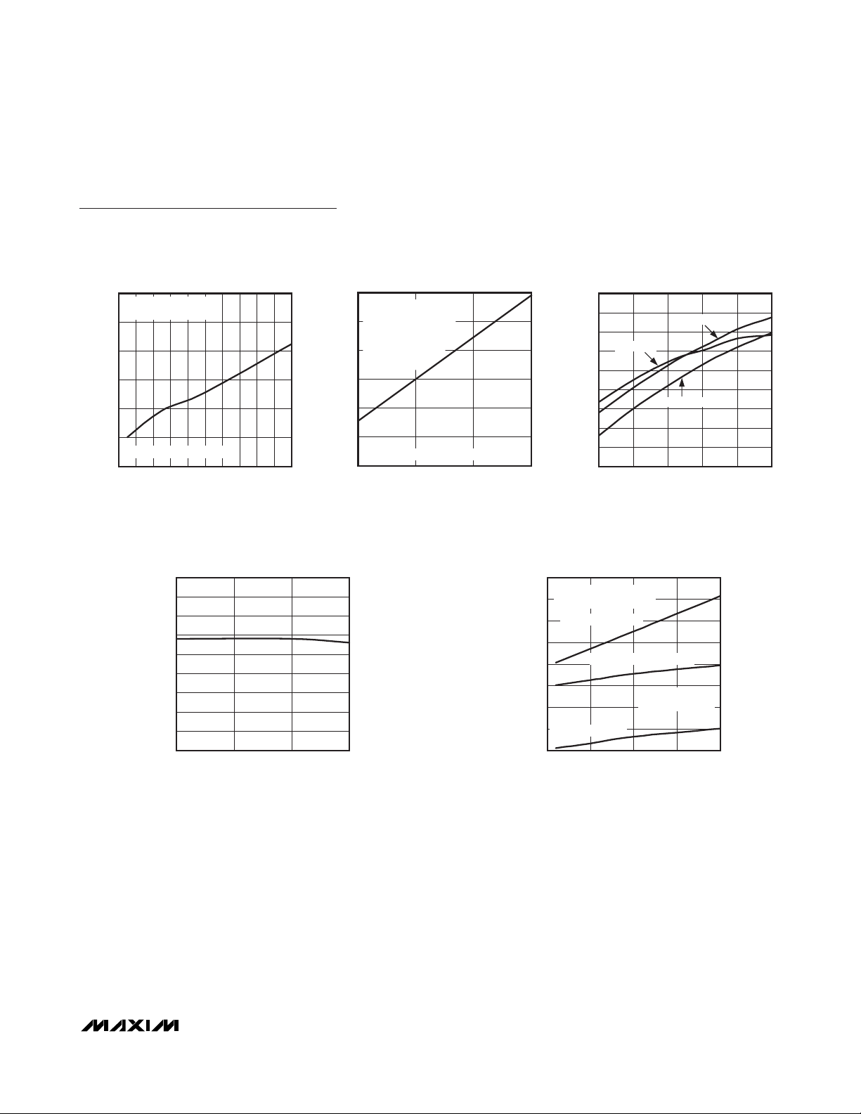
Typical Operating Characteristics
(VDD= 1.8V at TA= -40°C to +85°C (TA= -40°C, TA= 0°C, TA= +25°C, and TA= +85°C), 12-bit mode, all measurements using
noncontinuous AUX input. SPI = 10MHz and I
2
C = 400kHz, unless otherwise noted. Resistive touch-screen panel (X+ to X- = 608Ω,
Y+ to Y- = 371Ω).)
AVERAGE SUPPLY CURRENT
vs. SAMPLING RATE
90
AUTONOMOUS MODE
80
MAX11800
MAX11801
70
60
50
40
30
SUPPLY CURRENT (FA)
20
DATA TAKEN WITH
10
RESISTIVE TOUCH
SENSOR
0
0 200
SAMPLING RATE (cps)
cps = COORDINATES
PER SECOND
180160120 14040 60 80 10020
AVERAGE SUPPLY CURRENT
vs. SAMPLING RATE
5
DIRECT EDGE
INTERRUPT MODE
4
3
2
1
0
0 200
cps = COORDINATES PER SECOND
SAMPLING RATE (cps)
MAX11800 toc01
AVERAGE SUPPLY CURRENT
vs. SAMPLING RATE
5
DIRECT CONTINUOUS
INTERRUPT MODE
4
3
2
SUPPLY CURRENT (FA)
1
0
0 200
cps = COORDINATES PER SECOND
SAMPLING RATE (cps)
MAX11800 toc02
SUPPLY CURRENT (FA)
18016014012010080604020
18016014012010080604020
MAX11800 toc03
0.40
0.36
0.32
0.28
0.24
0.20
0.16
0.12
0.08
POWER-DOWN SUPPLY CURRENT (µA)
0.04
0
-40 85
vs. TEMPERATURE
TEMPERATURE (NC)
8
MAX11800 toc04
603510-15
7
6
(I)
ON
R
X+
5
X-
4
3
1.6 3.6
CHANGE IN ADC GAIN
vs. TEMPERATURE
4
SUPPLY CURRENT IN POWER-DOWN
3
2
1
0
-1
DELTA FROM +25NC (LSB)
-2
-3
-4
-40 110
TEMPERATURE (NC)
8050-10 20
MAX11800 toc07
SWITCH RESISTANCE
vs. SUPPLY VOLTAGE
Y+
Y-
VDD (V)
SWITCH RESISTANCE
vs. TEMPERATURE
7
6
MAX11800 toc05
5
(I)
4
ON
R
3
2
3.22.82.42.0
1
-40 85
Y+
MAX11800 toc06
X+
Y-
X-
603510-15
TEMPERATURE (NC)
CHANGE IN ADC OFFSET
vs. TEMPERATURE
4
3
2
1
0
-1
DELTA FROM +25NC (LSB)
-2
-3
-4
-40 110
TEMPERATURE (NC)
8050-10 20
MAX11800 toc08
Page 13
MAX11800–MAX11803
Low-Power, Ultra-Small Resistive Touch-Screen
Controllers with I2C/SPI Interface
______________________________________________________________________________________
13
Typical Operating Characteristics (continued)
(VDD= 1.8V at TA= -40°C to +85°C (TA= -40°C, TA= 0°C, TA= +25°C, and TA= +85°C), 12-bit mode, all measurements using
noncontinuous AUX input. SPI = 10MHz and I
2
C = 400kHz, unless otherwise noted. Resistive touch-screen panel (X+ to X- = 608Ω,
Y+ to Y- = 371Ω).)
AVERAGE SUPPLY CURRENT
vs. SAMPLING RATE
3.0
DIRECT CONVERSION
MODE—AUXILIARY INPUT
2.5
2.0
1.5
1.0
SUPPLY CURRENT (FA)
0.5
sps = SAMPLES PER SECOND
0
0 200
SAMPLING RATE (sps)
18016014012010080604020
INTERNAL OSCILLATOR CLOCK
FREQUENCY vs. SUPPLY VOLTAGE
2.08
2.06
2.04
2.02
2.00
1.98
1.96
1.94
1.92
INTERNAL OSCILLATOR CLOCK FREQUENCY (MHz)
1.90
1.8 3.6
VDD (V)
MAX11800 toc09
AVERAGE SUPPLY CURRENT
vs. SAMPLING RATE
120
AUXILIARY INPUT DATA
SAMPLED AT 1ksps AND
100
2ksps WITH EIGHT AND
16 SAMPLES
80
AVERAGING
ENABLED
60
40
SUPPLY CURRENT (FA)
20
0
ksps = KILO-SAMPLES PER SECOND
832
EQUIVALENT SAMPLING RATE (ksps)
2416
2.08
2.06
MAX11800 toc10
2.04
2.02
2.00
1.98
1.96
1.94
1.92
INTERNAL OSCILLATOR CLOCK FREQUENCY (MHz)
1.90
INTERNAL OSCILLATOR CLOCK
FREQUENCY vs. TEMPERATURE
V
DD
V
= 1.8V
DD
V
= 3.6V
DD
-40 85
TEMPERATURE (NC)
POWER CONSUMPTION
vs. SAMPLE RATE
160
DATA TAKEN WITH
140
MAX11800 toc12
3.02.4
*MAX11800/MAX11801
RESISTIVE TOUCH SENSOR
AUTONOMOUS MODE*
120
100
80
60
40
POWER CONSUMPTION (FW)
20
0
0 200
DIRECT CONTINUOUS MODE
cps = COORDINATES
PER SECOND
DIRECT EDGE MODE
SAMPLE RATE (cps)
15010050
= 3.0V
603510-15
MAX11800 toc13
MAX11800 toc11
Page 14

MAX11800–MAX11803
Low-Power, Ultra-Small Resistive Touch-Screen
Controllers with I2C/SPI Interface
14 ______________________________________________________________________________________
Pin Description
PIN
MAX11800/MAX11802 MAX11801/MAX11803
TQFN-E P WL P TQFN- EP WLP
1 A4 1 A4 X+ X+ Channel Input/Output
2 B4 2 B4 VDD Power Supply. Bypass VDD to GND with a 1μF capacitor.
3 B3 3 B3 GND Ground
4 C4 4 C4 X- X- Channel Input/Output
5 C3 5 C3 Y- Y- Channel Input/Output
6 C2 6 C2 TIRQ Active-Low Touch Interrupt Output
7 C1 — —- DIN SPI Serial Data Input
8 B1 — — CLK SPI Serial Data Cloc k Input
9 A1 — — CS SPI Chip-Select Input
10 B2 — — DOUT SPI Data Output
11 A2 11 A2 AUX Auxiliary Input
12 A3 12 A3 Y+ Y+ Channel Input/Output
— — 7 C1 SDA I2C Serial Data Bus Input/Output
— — 8 B1 SCL I2C Serial Data Clock Input
— — 9 A1 A0 I2C Address Input Bit 0
— — 10 B2 A1 I2C Address Input Bit 1
— — — — EP Exposed Pad (TQFN only). Connected to ground.
NAME FUNCTION
Page 15
MAX11800–MAX11803
Low-Power, Ultra-Small Resistive Touch-Screen
Controllers with I2C/SPI Interface
______________________________________________________________________________________ 15
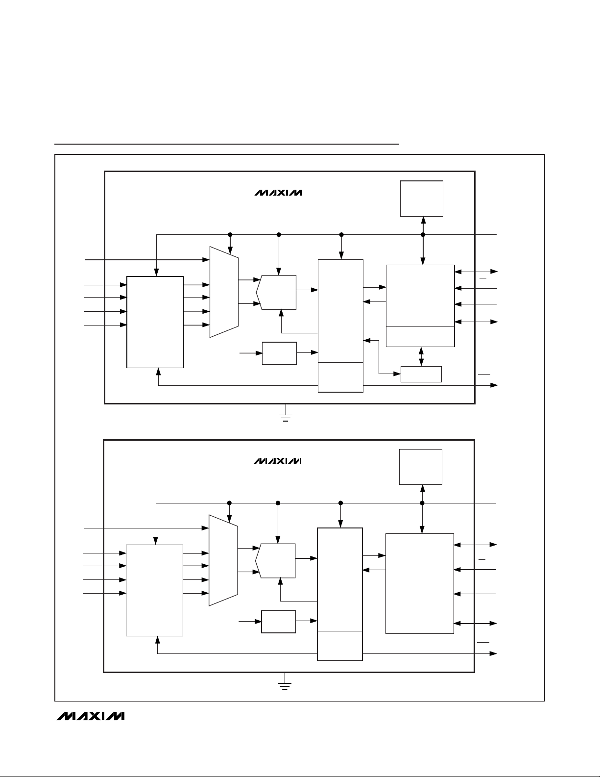
Functional Diagrams
AUX
POWER
MAX11800/MAX11801
X+
X-
Y+
Y-
TOUCHSCREEN
INTERFACE
MUX
SAR
ADC
LOGIC
CORE
V
DD
INTERNAL
CLOCK
INTERRUPT
GENERATION
ENGINE
GND
AND
BIAS
SERIAL INTERFACE
PHYSICAL LAYER
(ANALOG INTERFACE)
SIF
PHY
AUTONOMOUS
MODE ENGINE
FIFO
V
DD
DOUT (A1)
CS (A0)
CLK (SCL)
DIN (SDA)
TIRQ
AUX
POWER
MAX11802/MAX11803
X+
X-
Y+
Y-
TOUCHSCREEN
INTERFACE
MUX
SAR
ADC
LOGIC
CORE
V
DD
INTERNAL
CLOCK
INTERRUPT
GENERATION
ENGINE
GND
AND
BIAS
SERIAL INTERFACE
PHYSICAL LAYER
(ANALOG INTERFACE)
SIF
PHY
V
DD
DOUT (A1)
CS (A0)
CLK (SCL)
DIN (SDA)
TIRQ
Page 16

MAX11800–MAX11803
Low-Power, Ultra-Small Resistive Touch-Screen
Controllers with I2C/SPI Interface
16 ______________________________________________________________________________________
Detailed Description
The MAX11800–MAX11803 contain standard features
found in a typical resistive touch-screen controller as
well as advanced features found only on Maxim touchscreen controllers. Standard features included in the
MAX11800–MAX11803 are:
• 4-wire touch-screen interface
• X/Y coordinate measurement
• Touch pressure measurement
• Direct conversion operation—requires direct AP
involvement
• Single commands—AP initiates all activity, one
command at a time
• Ratiometric measurement
• 12-bit SAR ADC
• Single 1.7V to 3.6V supply
• Programmable touch-detect pullup—50kΩ or
100kΩ
• Auto power-down control for low-power operation
Advanced features found in the MAX11800/MAX11801
include:
• Autonomous conversion operation—minimal AP
involvement
• On-chip FIFO—buffers up to 16 consecutive mea-
surements
• Data tagging—records measurement and touch-
event information
• Filtering—reduces noise using straight or median
averaging
• Aperture mode—provides spatial filtering
• Combined commands—multiple operations per-
formed with a single AP command
• User-programmable acquisition modes
• Programmable interrupt output drive
Advanced features found in the MAX11802/MAX11803
include:
• Data tagging—records measurement and touch
event information
• Filtering—reduces noise using straight or median
averaging
• Combined commands—multiple operations performed with a single AP command
• User-programmable acquisition modes
• Programmable interrupt output drive
The MAX11800/MAX11801 operate in one of two toplevel modes: direct conversion mode (DCM) or
autonomous conversion mode (ACM). Direct conversion mode requires the AP to initiate all activity to and
from the MAX11800/MAX11801. DCM is the operating
mode that most standard resistive touch-screen controllers use. ACM allows the MAX11800/MAX11801 to
perform measurements automatically and inform the AP
when they are complete, reducing data transfers on the
serial bus as well as generating fewer interrupt
requests. The MAX11802/MAX11803 operate in DCM
only. DCM requires the AP to initiate all activity to and
from the MAX11802/MAX11803. DCM is the operating
mode that most standard resistive touch-screen controllers use.
Both DCM and ACM support averaging, data tagging,
and combined commands. Certain commands and
operations are only available in DCM, while others are
only available in ACM. See Figures 3a and 3b and
Table 2 for details.
Position Measurements
Position measurements determine either the X or Y
coordinates of the point of contact on the panel sensor.
Allow adequate time for the panel to settle when switching between X and Y measurements. Figure 4 shows
the physical setup of the panel when performing position measurements.
The element R
TOUCH
represents the resistance between
the X and Y planes of the panel sensor. R
TOUCH
does
not contribute to the error when performing position
measurements. R
TOUCH
affects the panel settling time
required between each valid measurement.
The panel end-to-end resistance in the direction of
measurement determines the power applied across the
panel. The panel dissipates power in the X elements
when performing an X direction measurement and dissipates power in the Y elements when performing a Y
direction measurement.
Page 17
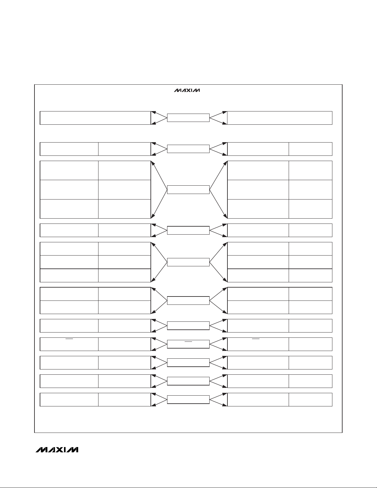
MAX11800–MAX11803
Low-Power, Ultra-Small Resistive Touch-Screen
Controllers with I2C/SPI Interface
______________________________________________________________________________________ 17
Figure 3a. MAX11800/MAX11801 Operation Modes
MAX11800/MAX11801
OPERATION MODES
DIRECT CONVERSION MODE
CONFIGURATION REGISTER 0x0B BITS[6:5] = 00
CONFIGURATION
REGISTERS
PANEL TIMING
0x05
N/A
N/A
AUX
0x0A
AVERAGING METHOD
0x03, 0x0B
EDGE INTERRUPT MODE
0x01
CONTINUOUS INTERRUPT MODE
0x01
N/A N/A
EVENT TAG (ETAG)
(FIFO NOT USED)
MEASUREMENT TAG (MTAG)
(FIFO NOT USED)
AND READBACK COMMANDS
DATA READBACK: 0x52–0x59
DATA READBACK: 0x52–0x59
DATA READBACK: 0x5A–0x5B
DATA READBACK: 0x52–0x59 FIFO READBACK: 0x50
DATA READBACK: 0x52–0x59
SETUP, MEASUREMENTS,
PANEL SETUP
0x69–0x6F
COMBINED MEASUREMENT
MEASUREMENT: 0x70–0x75
PANEL MEASUREMENT
MEASUREMENT: 0x78–0x7F
AUX MEASUREMENT
MEASUREMENT: 0x76–0x77
N/A
N/A N/A N/A
N/A N/A N/A
OPERATION MODE
PANEL SETUP
MEASUREMENTS
AVERAGING
INTERRUPTS
DATA TAGGING
AUTONOMOUS CONVERSION MODE
CONFIGURATION REGISTER 0x0B BITS[6:5] = 01, 10, 11
CONFIGURATION
REGISTERS
PANEL TIMING (1)
0x05
COMBINED MEASUREMENT
0x0B
N/A N/A
N/A N/A
AVERAGING METHOD (1)
0x03, 0x0B
CLEAR-ON-READ
INTERRUPT (1)
EVENT TAG (ETAG)
(USES FIFO)
MEASUREMENT TAG (MTAG)
(USES FIFO)
SETUP, MEASUREMENTS,
AND READBACK COMMANDS (2)
N/A
MEASUREMENT: N/A
FIFO READBACK: 0x50
N/A
N/A
FIFO READBACK: 0x50
N/A N/A
TIRQ
0x01
ADC RESOLUTION AND TIMING
0x02, 0x04, 0x06
PUR AND PUF TIMING
0x07
N/A
NOTE 1: THE CONFIGURATION REGISTERS MUST BE SET UP PRIOR TO ENTERING AUTONOMOUS MODE. THESE REGISTERS CANNOT BE ALTERED WHILE AUTONOMOUS MODE IS ACTIVE.
NOTE 2: COMMANDS RECEIVED WHILE AUTONOMOUS MODE IS ACTIVE ARE IGNORED (EXCEPT READBACK COMMANDS). DURING AUTONOMOUS MODE ALL SCAN ACTIVITIES ARE
CONTROLLED BY THE MAX11800/MAX11801, BASED ON THE SETTINGS OF THE CONFIGURATION REGISTERS. ALL MEASUREMENT RESULTS ARE STORED IN THE ON-CHIP FIFO.
N/A N/A
N/A N/A
N/A N/A
N/A N/A
APERTURE
TIRQ
ADC
TDM TIMING
AUTONOMOUS TIMING
APERTURE SETTING (1)
0x09, 0x0B
TIRQ (1)
0x01
ADC RESOLUTION AND TIMING (1)
0x02, 0x04, 0x06
PUR AND PUF TIMING (1)
0x07
TINT AND SCANP TIMING (1)
0x08
N/A
Page 18
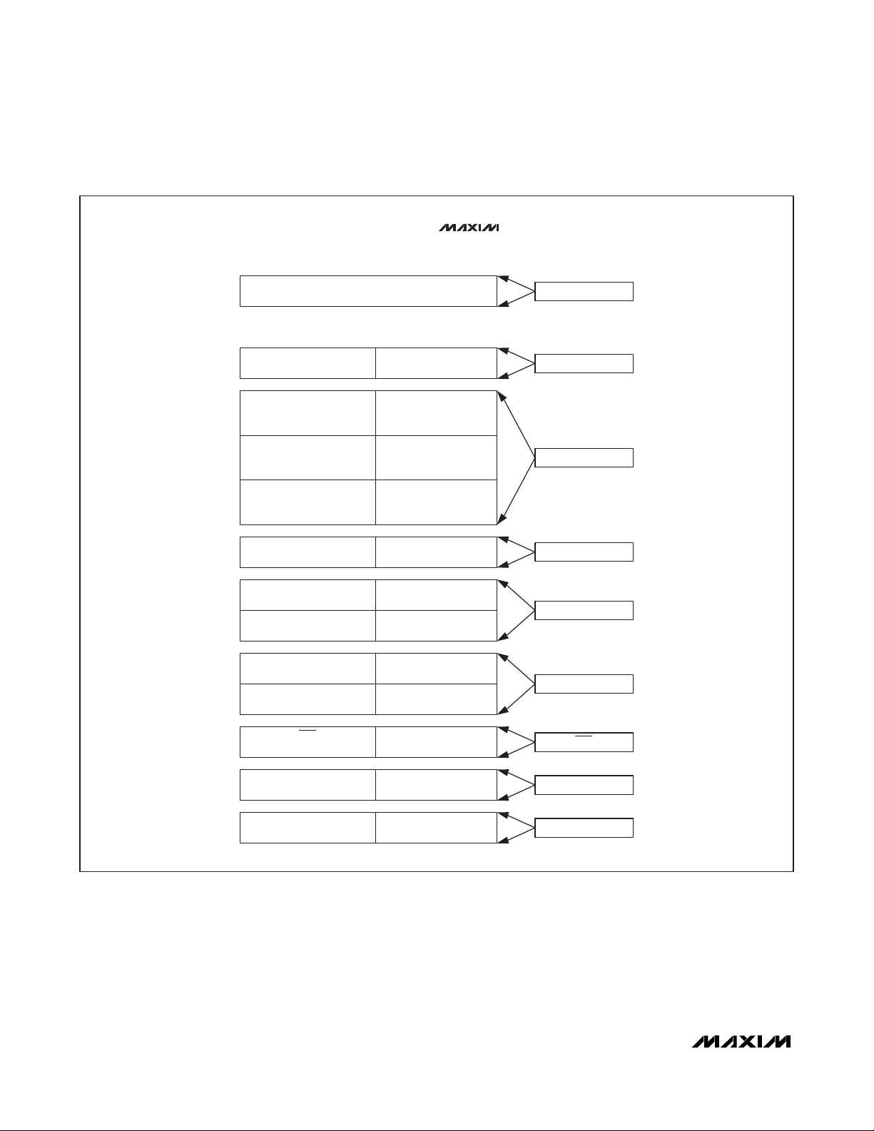
MAX11800–MAX11803
Low-Power, Ultra-Small Resistive Touch-Screen
Controllers with I2C/SPI Interface
18 ______________________________________________________________________________________
Figure 3b. MAX11802/MAX11803 Operation Modes
MAX11802/MAX11803
OPERATION MODES
DIRECT CONVERSION MODE
CONFIGURATION
REGISTERS
PANEL TIMING
0x05
N/A
N/A
AUX
0x0A
AVERAGING METHOD
0x03, 0x0B
EDGE INTERRUPT MODE
0x01
CONTINUOUS INTERRUPT MODE
0x01
EVENT TAG (ETAG)
(FIFO NOT USED)
MEASUREMENT TAG (MTAG)
(FIFO NOT USED)
SETUP, MEASUREMENTS,
AND READBACK COMMANDS
PANEL SETUP
0x69–0x6F
COMBINED MEASUREMENT
MEASUREMENT: 0x70–0x75
DATA READBACK: 0x52–0x59
PANEL MEASUREMENT
MEASUREMENT: 0x78–0x7F
DATA READBACK: 0x52–0x59
AUX MEASUREMENT
MEASUREMENT: 0x76–0x77
DATA READBACK: 0x5A–0x5B
N/A
N/A
N/A
DATA READBACK: 0x52–0x59
DATA READBACK: 0x52–0x59
OPERATION MODE
PANEL SETUP
MEASUREMENTS
AVERAGING
INTERRUPTS
DATA TAGGING
TIRQ
0x01
ADC RESOLUTION AND TIMING
0x02, 0x04, 0x06
PUR AND PUF TIMING
0x07
N/A
N/A
N/A
TIRQ
ADC
TDM TIMING
Page 19

MAX11800–MAX11803
Low-Power, Ultra-Small Resistive Touch-Screen
Controllers with I2C/SPI Interface
______________________________________________________________________________________ 19
Pressure Measurements
Z1 and Z2 measurements determine the resistance
between the two planes within the panel sensor during
a touch (R
TOUCH
). Depending on the known physical
properties of the panel, one of two equations extract the
value of R
TOUCH
, providing information about the pressure and area of the touch applied to the panel. Allow
adequate time for the panel to settle when switching
between position and pressure measurements. Figure 5
shows the physical setup of the panel when performing
pressure measurements.
Z1 and Z2 measurements allow observation of the voltage on either side of the effective R
TOUCH
resistance.
With both Z1 and Z2 measurements available, compute
R
TOUCH
as follows:
If only a Z1 measurement is available, compute
R
TOUCH
as follows:
The power applied across the panel during pressure
measurements is greatly dependent on R
TOUCH
and
the physical position of the touch. The maximum power
dissipation in the panel during a pressure measurement
is approximately PZ= V
DD
2
/R
TOUCH
. This maximum
Table 2. Operating Modes, Conditions, and Options
1
In ACM, the choices are limited to X and Y scan, or X and Y and Z1 scan, or X and Y and Z1 and Z2 scan.
2
In DCM, MTAG is always used. For DCM with CONT = 0, the following ETAGs are used: 00 = touch present (data valid), 10 = no
touch present (data may be invalid), 11 = measurement in progress (data invalid). For DCM with CONT = 1, the panel cannot be
scanned for a touch because panel setup switches are configured in a measurement mode; therefore, ETAG = 00 is used if a measurement is not in progress, or ETAG = 11 if a measurement is in progress.
3
A separate configuration register for delay time, sampling time, averaging, and ADC resolution settings configures the AUX input.
Figure 5. Pressure Measurements
Figure 4. Position Measurements
⎞
−
1
⎟
⎠
Y
POSITION
N
2
BIT
COR
INT
YY
OPERATION
MODE
DCM
MAX11800–
PUR
PSU PMC CMC TDM LPM AVG FIFO APER
CONT MTAG ETAG
PUF
Yes Yes Yes Yes No Yes No No Yes Yes Yes
2
Yes 2Yes Yes Yes No
X, Y,
Z1, Z2
EINT CINT
MAX11803
ACM
MAX11800/
1
Yes
Yes 1 Yes 1 Yes Yes Yes Yes Yes Yes No Yes Yes Yes No No Yes
MAX11801
AUX No Yes 3 No No — Yes 3No No No No No No No No No No
RR
TOUCH XPLATE
=
TOUCH
RX
⎛
XPLATE POSITION
=
⎜
N
⎝
BITX
2
R
XZ
⎛
⎜
⎝
2
⎞
⎛
⎟
⎜
⎠
⎝
POSITION
N
2
N
BI
TTZ
Z
1
⎞
⎛
2
⎟
⎜
⎠
BITX
11
−
⎝
Z
1
R
YPLATE
⎛
⎜
⎝
⎞
−−
⎟
⎠
⎞
⎟
⎠
ADC
INPUT
PANEL
R
TOUCH
X-
X POSITION MEASUREMENT
Y+
Y-
X+
V
DD
PANEL
R
X-
Y POSITION MEASUREMENT
TOUCH
ADC
INPUT
V
Y+
DD
Y-
X+
PANEL
R
TOUCH
X-
Z1 PRESSURE MEASUREMENT
ADC
INPUT
X+
V
Y+
DD
PANEL
R
TOUCH
Y-
X-
Z2 PRESSURE MEASUREMENT
V
Y+
DD
ADC
INPUT
Y-
X+
Page 20

MAX11800–MAX11803
Low-Power, Ultra-Small Resistive Touch-Screen
Controllers with I2C/SPI Interface
20 ______________________________________________________________________________________
power dissipation condition is observed when the point
of contact is in the top left corner of the panel sensor.
The planar end-to-end resistance included in the current path is minimal at this location. Keep the averaging
and panel settling durations to the minimum required
by the application when pressure measurements are
required. Table 3 summarizes the physical panel settings for supported measurement types.
Touch-Detect Modes and Options
Figure 6 shows the internal circuitry in the
MAX11800–MAX11803 used to detect the presence of
a touch on the panel. The selection of the pullup resistance value (RTD= touch-detect resistance) and the
durations of the rough pullup interval (PUR = lowimpedance pullup) and fine pullup interval (PUF = highimpedance pullup) are user-defined.
The MAX11800–MAX11803 revert to the low-power
panel setup when placed in touch-detect mode (TDM).
Figure 6 shows the active panel drive switches (YMSW
and XPSW are omitted for simplicity). TSW is a dedicated pullup switch used in TDM. TSW is also used during
PUF and TDM. XPSW is activated during PUR periods.
TDRSEL allows the selection of an internal pullup resistor value of either 50kΩ or 100kΩ.
The X and Y touch-screen plates create an open circuit
with no current flow in the panel when the panel is not
being touched. In this case, TOUCH (see Figure 6) is
low. When a touch causes contact between the panel X
and Y plates, a current path is created and TOUCH is
pulled high, as long as R
PX
+ RPY(the sum of panel
end-to-end resistance) is much lower than RTD. Typical
open-circuit panel plate resistances range from 200Ω
to 1000Ω.
The MAX11800–MAX11803 enter high-impedance
pullup mode (50kΩ or 100kΩ) when the panel is not
being touched. The device is idle in this mode until a
touch is detected. The YMSW and TSW transistors are
on, and the XPSW and PSW transistors are off. With no
touch present, the Y- input of the TSC is at ground and
the X+ input is at V
DD
- VTN, where VTNis the threshold
voltage of the TSW nMOS device. This is a low-power
mode in which no current is consumed until a panel
touch occurs. When a touch is present on the panel,
the touch-screen controller (TSC) X+ input is pulled low
by the touch panel plate resistance and the YMSW transistor. This causes TOUCH to assume a logic-high and
the devices either issue the TIRQ interrupt for direct
conversion modes (MAX11800–MAX11803) or begin
self-timed scans for autonomous conversion mode
(MAX11800/MAX11801).
The value of the user-defined RTDdepends on the
characteristics of the panel. To ensure reliable
detection values, worst-case panel resistance must
be checked against RTD. The interaction between
RTDand the panel (or external noise rejecting)
capacitance determines how quickly the panel can
be switched from measurement modes back to
touch monitoring mode without reporting false
touches or erroneous tags due to panel settling.
Panel touch status is also required to tag data from a
completed scan and measurement operation. Following
each scan operation, the panel must be returned to
TDM to determine if the panel is still being touched and
if the data obtained during the scan operation should
be considered valid. This operation is required since
the panel cannot be monitored for the presence of a
touch during the scan and measurement procedure.
The MAX11800–MAX11803 must return to TDM after
completing a measurement and making a decision on
the touch status of the panel. The measurement procedure is only completed upon resolution of the touch status and when data is tagged and available for
readback. The characteristics of the return to TDM and
Table 3. Summary of Physical Panel Settings for Supported Measurement Types
Note: The ADC input is fully differential with the negative input internally connected to GND. The MAX11800–MAX11803 control
access to the PUR, PUF, TDM, and LPM, which do not require setup procedures.
U
indicates unconnected node.
MODE X+ X- Y+ Y- REF+ REF-
XVDDGND ADC_IN U X+ X-
Y ADC_IN U V
Z1 ADC_IN GND V
Z2 U GND V
PUR VDD (10Ω) U U GND U —
V
through
TDM or PUF
LPMUUUUU—
DD
50kΩ or 100kΩ
U U GND U —
DD
DD
DD
GND Y+ Y-
UY+X-
ADC_IN Y+ X-
Page 21

MAX11800–MAX11803
Low-Power, Ultra-Small Resistive Touch-Screen
Controllers with I2C/SPI Interface
______________________________________________________________________________________ 21
the timing of the decision are configurable through the
touch-detect pullup timing configuration register (0x07).
Program the MAX11800–MAX11803 in the context of
the application to maximize power efficiency and
achieve the desired scan throughput.
PUR and PUF
PUR is a fast pullup mode, which uses the main X+
switch in parallel with the resistive pullup to quickly slew
the panel capacitance. PUF uses only the touch-detect
pullup resistor, RTD. PUR and PUF serve the same function as TDM, but are timed so that the panel can settle
after completing measurements and before rendering
any decisions on the touch status of the panel.
Use the optional PUR mode to reduce the time to tag
data by momentarily placing the panel in a low-impedance (< 10Ω) pullup mode instead of using the available 50kΩ/100kΩ touch-detection pullup resistors. This
operation forces the monitored TSC input high during
the PUR interval. Once the PUR interval expires, a PUF
interval must be allowed so that the panel can recover
and pull the TSC input low in case a touch is present.
The purpose of the PUR mode is to reduce the time
required to determine touch status by avoiding long
pullup time constants caused by high-capacitance
touch panels and the high-impedance on-chip pullup
resistors (RTD). When a touch is present during PUR
intervals, the current through the low-impedance pullup
(XPSW) and panel combination is significantly higher
than that observed in the PUF mode. The durations in
the PUR mode should be matched to the panel characteristics and the desired scan throughput rates to minimize power dissipation.
While use of the PUR mode is optional, the PUF period
is required for all applications. The PUF interval allows
the panel to resettle following scan or optional PUR
intervals. When a touch is not present, the panel capacitance settles toward V
DD
through the internal pullup
switch and a portion of the panel resistance (with the
optional PUR mode disabled). When a touch is present,
the panel capacitance settles toward ground through a
portion of the panel resistance, ideally significantly
lower than the selected pullup impedance, RTD. Allow
enough recovery time for settling through the panel
resistance when using a PUR mode. Figure 7 illustrates
the touch-detection operations.
Idle Modes
Once the PUF period expires, the preceding measurement data is tagged and made available for readback.
The MAX11800–MAX11803 transition to an appropriate
mode depending on the conversion and interrupt mode
selected.
Features Available in the
MAX11800–MAX11803 Averaging Modes
The MAX11800–MAX11803 contain a programmable
averaging filter. When enabled, this feature allows collecting 4, 8, or 16 consecutive samples for each measurement type requested. The number of the samples
for each measurement type is controlled by configuration register 0x03. Averaging can be assigned to each
measurement type. For example, X and Y measurements can use an average of 16 samples, while Z measurements can use one or four samples to save power.
The AUX depth is selected in configuration register
0x0A.
The MAX11800–MAX11803 can be configured to perform one of two statistical operations. One option is a
median averaging filter (MAF). The MAF first removes
the lowest and highest values before averaging the
remaining sample set. The second filter type is a
straight averaging filter (SAF), which takes the average
of the entire sample set. Both filter types and
position/pressure averaging are controlled by configuration register 0x0B. Table 4 presents the details of the
median averaging operations of the MAX11800–
MAX11803. For the MAX11800/MAX11801, averaging is
supported in both direct conversion mode and
autonomous conversion mode. The MAX11802/
MAX11803 support only direct conversion mode.
Figure 6. Touch-Detection Circuitry
V
DD
PSW
TDRSEL
RTD RTD
Y+
XPSW
PUR
X-
PANEL
X+
Y-
YMSW
PUR, PUF, TDM
TSW
PUR, PUF, TDM
TOUCH
(TO MAX11800/
MAX11801 LOGIC)
MAX11800–
MAX11803
Page 22

MAX11800–MAX11803
Low-Power, Ultra-Small Resistive Touch-Screen
Controllers with I2C/SPI Interface
22 ______________________________________________________________________________________
Figure 7. Touch-Detection Operations
FAST PULLUP TOUCH DETECTION (NOTE: INCREASED CURRENT IN PUR MODE DURING TOUCH)
DIGITAL WAVEFORM
(OPTIONAL)
MEASUREMENT COMPLETE—
DATA IS KNOWN
ANALOG WAVEFORM
V
DD
TSC INPUT
INITIAL INPUT VOLTAGE
DETERMINED BY LAST SCAN
ACTIVITY
NORMAL TOUCH DETECTION (NOTE: NO PUR PERIOD; ALLOW LONG PULLUP TIMES)
DIGITAL WAVEFORM
POWER ASSISTED PULLUP PERIOD (10Ω) PANEL IS ALLOWED TO RESETTLE BEFORE
FORCED FAST PULLUP USING
10Ω SWITCH
DATA VALIDITY IS DETERMINED
(DATA IS TAGGED)
PUF MODESCAN MODE
DETERMINING DATA VALIDITY
TIME
DATA VALIDITY IS DETERMINED
(DATA IS TAGGED)
TOUCH DETECTPUR MODE
IS THERE A TOUCH?
YES = LPM.
NO = TDM.
TOUCH NOT PRESENT: TSC INPUT
REMAINS HIGH
TOUCH PRESENT:
TSC INPUT PULLED LOW
TOUCH DETECTPUF MODESCAN MODE
MEASUREMENT COMPLETE—
DATA IS KNOWN
ANALOG WAVEFORM
V
DD
TSC INPUT
INITIAL INPUT VOLTAGE
DETERMINED BY LAST SCAN
ACTIVITY
PANEL IS ALLOWED TO RESETTLE BEFORE DETERMINING DATA VALIDITY
(THROUGH 50kΩ/100kΩ PULLUP)
TOUCH NOT PRESENT:
TSC INPUT PULLED HIGH THROUGH 50kΩ/100kΩ PULLUP
TOUCH PRESENT:
TSC INPUT PULLED LOW BY PANEL
TIME
IS THERE A TOUCH?
YES = LPM.
NO = TDM.
Page 23

MAX11800–MAX11803
Low-Power, Ultra-Small Resistive Touch-Screen
Controllers with I2C/SPI Interface
______________________________________________________________________________________ 23
Combined Commands
Combined commands reduce AP interaction with the
MAX11800–MAX11803 by allowing multiple measurements. For example, the MAX11800–MAX11803 can be
instructed to provide X and Y data, or X and Y and Z1
data, or X and Y and Z1 and Z2 data using a single
command.
Data Tagging
In direct conversion modes, all measurement data is
contained in a 16-bit word. X, Y, Z1, and Z2 information
is stored independently. Each word consists of 12 bits
of measurement data plus a 2-bit measurement type
(MTAG) and a 2-bit event tag (ETAG). The measurement tag identifies whether the data represents an X, Y,
Z1, or Z2 result. The event tag indicates the point at
which the data is sampled (initial, midpress, or release)
during the touch event. When trying to read a result that
is pending, the entire data stream is read back as
FFFFh and the event tag as 11b, indicating that the corresponding measurement is in progress and that the
data stream is to be ignored. For combined commands,
all data locations requested by the command are
marked FFFFh, pending the completion of the entire
command and the proper tagging of the data. See
Table 5.
Direct conversion modes do not use the internal FIFO
or support the aperture function (see the
Aperture
Modes and Options
section). Each measurement type
uses a single location in the (16-bit) memory. The AP
must retrieve the data from the last requested measurement before moving on to the next measurement of the
type.
Auxiliary measurement data is not tagged because it is
not related to panel operation. Auxiliary measurement
data is stored and read back identically to the other
direct conversion data. The tag locations for auxiliary
measurement data are always set to 0000b, unless the
read occurs when an auxiliary measurement is in
progress. In this situation, the tag locations read 1111b
and the data stream reads back FFFFh.
Low-Power Modes
There are also two low-power modes, LPM and TDM.
LPM only applies when in DCM with edge interrupt
mode or ACM during periods following a conversion
where the panel was observed to be touched and a
subsequent panel measurement is required and/or
scheduled.
During LPM, all circuitry is off, including the on-chip
touch-detect pullup resistors used in the touch-detect
circuitry. In direct conversion modes, a user-request initiates the next operation and all circuitry is off until a
user-command is received. Therefore, the current consumption is primarily due to junction leakage. In
autonomous conversion mode, an on-chip oscillator
and timer are constantly running. Therefore, the device
current consumption is primarily determined by the
oscillator and timer.
During TDM, all circuitry is off except the on-chip pullup
resistor. This is an untimed mode (oscillator and timer
are off) for both ACM and DCM (no digital current). This
mode only consumes current through the on-chip
pullup resistor when a touch is present. The device can
be powered down through register 0x0B when no panel
input is expected or needed, and, therefore, no power
is consumed through the panel.
Table 5. Data Word Structure (All Direct Conversion Modes)
Table 4. Median Averaging Operations
*
When using averaging with 8-bit conversions, these positions may be filled with fractional data due to averaging operations.
NUMBER OF
REMAINING SAMPLES
AVERAGED
AVERAGING MODE
14112
28224
3164 4 8
NUMBER OF
SAMPLES TAKEN
NUMBER OF HIGH
SAMPLES REMOVED
NUMBER OF LOW
SAMPLES REMOVED
INDEX 1514131211109876543210
Byte MSB Byte LSB Byte
12-Bit Content Position MSBs Position LSBs Measure Event
8-Bit Content Posit ion Data Trailing Zeros* Measure Event
Page 24

MAX11800–MAX11803
Low-Power, Ultra-Small Resistive Touch-Screen
Controllers with I2C/SPI Interface
24 ______________________________________________________________________________________
Features Available in the
MAX11800/MAX11801 Only
Autonomous Mode
The MAX11800/MAX11801 can perform measurements
automatically without the AP involvement, and is
referred to as autonomous conversion mode (ACM).
When operating in ACM, the MAX11800/MAX11801 use
an on-chip FIFO to store measurement results. As each
new data is written to the FIFO, an interrupt is generated. The AP can choose to service (read) the FIFO result
after each interrupt or wait until the FIFO is full then
read the entire FIFO contents at once. The AP can also
read the contents of the FIFO at any time. See the
Autonomous Conversion Mode
section for a further
description of operations.
Aperture
The MAX11800/MAX11801 contain a feature referred to
as aperture. It is only available on the MAX11800/
MAX11801 when operating in autonomous conversion
mode. The aperture feature creates an invisible rectangle around a touch location within the MAX11800/
MAX11801 hardware. The size of the rectangle is user
programmable. One application of the aperture feature
is to provide “spatial hysteresis.” Spatial hysteresis can
be useful for applications that require lower resolution
touch accuracy without requiring the AP to handle the
mathematics involved to filter out extraneous data.
Another application would be to use the aperture feature to implement simple single finger or stylus gestures. See the
Using Aperture Mode
section for a
further description of operations.
Panel Setup, Measurement, and Scan Commands
To simplify measurement procedures, the MAX11800–
MAX11803 support three types of commands: panel
setup commands (PSU), panel measurement commands
(PMC), and combined measurement commands (CMC).
In direct conversion mode, the MAX11800/MAX11801
can use all three types of commands. Using individual
panel setup and measurement commands allow for a
high degree of customization based on decisions made
by the AP, while using combined commands significantly simplifies the complete measurement process
and reduces communications between the AP and the
MAX11800–MAX11803.
In autonomous mode, the MAX11800/MAX11801 use
combined commands to control and automate all
aspects of panel setup, measurements, and timing. See
the
Operating Mode Configuration Register (0x0B)
sec-
tion for more details.
Direct Conversion Mode Operations
In direct conversion mode, the AP requests individual
panel setup and conversion operations or automated
combinations of measurements (X and Y, X and Y and
Z1, or X and Y and Z1 and Z2 combined). Unlike
autonomous conversion modes, the AP maintains control
over the initiation of panel setup, measurements events,
and the sampling frequency. Figure 8 shows the state
machine transitions for direct conversion mode.
Interrupt Modes
The MAX11800–MAX11803 support two direct conversion interrupt modes. The two direct conversion modes
are the continuous interrupt mode (CINT) and the edge
interrupt mode (EINT).
Continuous Interrupt Mode
In continuous interrupt mode, the panel returns to TDM
and idle. The current status of the panel is then sent
through TIRQ. The continuous interrupt mode is the
least efficient mode in current consumption for long
duration of touches. The power consumption is approximated by P
TOUCH
= V
DD
2
/RPU. The power consumption levels observed when the panel is not touched is
limited by the junction leakage currents of the
MAX11800–MAX11803.
Procedure: The MAX11800–MAX11803 idle in TDM.
The TIRQ output goes low when a touch is detected on
the panel indicating to the AP that a touch is present
and a measurement operation starts.
The AP requests specific panel measurements through
the serial interface. TIRQ stays low during panel setup
and measurement operations. Once a measurement is
complete (with the “continuous” bit, CONT = 0, see
Table 1), the MAX11800–MAX11803 check for the continued presence of a touch on the panel and tag the data
accordingly (see Table 6). The duration of this operation
is programmable, specified in the touch-detect pullup
timing configuration register (0x07). After the data is
tagged, the data is available for readback through the
serial interface. The MAX11800–MAX11803 return to
TDM and return control of TIRQ to the TDM circuitry.
TIRQ stays low while a touch remains present, indicating
further measurements are required, otherwise TIRQ goes
high until a new touch is observed.
Continuous interrupt mode (CINT) allows the complete
control over the measurement operations and direct observation of the touch status of the panel. Figure 9 shows the
polling of TIRQ when other functions share the TIRQ bus. In
the illustration of Figure 9, no ‘10’ event tag is observed
because the release occurs during a TDM period.
Page 25

Edge Interrupt Mode
When a touch is present on the panel in edge interrupt
mode, the MAX11800–MAX11803 return to an untimed
high-impedance mode once data tagging operations are
complete. In edge interrupt mode, the duration of a touch
is determined by the tags applied to the measurement
data. Data tagged as initial (00) or midpress (01) indicates
the user needs to continue to scan the panel until a
release is observed. In this state, there is no need to continue monitoring the touch status prior to the next requested measurement. If a panel touch is not present, data is
tagged as release (10) and the MAX11800–MAX11803
idle in TDM continuously, issuing an interrupt only when
the next panel touch is initiated.
The operation described in the preceding paragraph
makes the edge interrupt mode more power-efficient
than the continuous interrupt mode. However, the edge
interrupt mode requires continuous scanning of the
panel until a release (10) event is observed. Otherwise,
the MAX11800–MAX11803 do not idle in TDM and are
not able to recognize a change in touch status. New
touches are not recognized and new interrupts are not
issued if a release event is not detected before stopping the conversion sequence.
MAX11800–MAX11803
Low-Power, Ultra-Small Resistive Touch-Screen
Controllers with I2C/SPI Interface
______________________________________________________________________________________ 25
Figure 8. State Machine Transitions (Direct Conversion Mode)—MAX11800–MAX11803
Table 6. Measurement and Event Tags
(Continuous Interrupt Mode)
SETUP
NO
COMMAND
NO
COMMAND
NO
COMMAND
X
PANEL
SETUP
Y
PANEL
SETUP
Z
PANEL
TOUCH
DETECT
TIME IS UP
DONE AND
X
CONTINUOUS
DETECT
LAST AND NOT
CONVERSION
USER COMMAND
INTERNAL TRANSITION
AVERAGE
NOT LAST OR
CONTINUOUS
CONTINUOUS
LAST
CONVERSION
Y
ACQUIRE
Z1
ACQUIREZ2ACQUIRE
TOUCHDETECT
FINE
PULLUP
MEASUREMENT MTAG[3:2]
X 00
Y 01
Z1 10
Z2 11
EVENT ETAG[1:0]
Touch (data valid) 00
N/A (not used) 01
No touch present (data invalid) 10
Measurement in progress (data invalid) 11
NOT LAST OR
AVERAGE
CONVERSION
AUX
ACQUIRE
CONTINUOUS
CONTINUOUS
TIME IS UP
DONE AND
CONTINUOUS
LAST AND NOT
LAST
CONVERSION
TOUCHDETECT
FINE
PULLUP
Page 26

MAX11800–MAX11803
Low-Power, Ultra-Small Resistive Touch-Screen
Controllers with I2C/SPI Interface
26 ______________________________________________________________________________________
Procedure: The EINT mode reduces TIRQ activity.
During EINT, the MAX11800–MAX11803 idle in a TDM.
TIRQ goes low when a new touch is detected on the
panel. TIRQ stays low for a fixed duration as specified
in the configuration register 0x01, indicating to the AP
that a touch is present and measurements are required.
The AP requests specific panel setups and measurements through the serial interface using panel setup
and conversion commands after TIRQ goes low. Once
a measurement is complete (with CONT = 0), the
MAX11800–MAX11803 check for the continued presence of a touch and tag the data accordingly. See
Table 7. The duration of this operation is programmable, specified in the
Touch-Detect Pullup Timing
Configuration Register (0x07)
section. After the data is
tagged, it is available for readback through the serial
interface. The MAX11800–MAX11803 do not return to
TDM when the panel touch is still present (ETAG = 00,
01), but remain in an LPM awaiting further measurement commands. The devices return to TDM when the
panel touch is no longer present (ETAG = 10) and
return control of the TIRQ interrupt to the TDM circuitry
to await the next touch event.
After a touch is indicated, the AP must continue to issue
conversion commands until the touch is removed, alerting the AP when the panel is released (by ETAG = 10).
The MAX11800–MAX11803 return to TDM and observe
the start of the next touch event. Panel commands
issued with CONT = 1 are not capable of fulfilling this
requirement.
The EINT mode provides the least interrupt activity and
the lowest power consumption. Use EINT mode for
general touch-screen applications and applications
requiring high resolution in space and time. When the
TIRQ bus is shared with other functions, poll the general status register (0x00) to detect the presence of an
interrupt. See Figure 10.
Table 7. Measurement and Event Tags
(Edge Interrupt Mode)
Figure 9. Continuous Interrupt Mode (Direct Conversion Mode)
BEGINNING OF TOUCH EVENT
PANEL
TOUCH
TIRQ
TDM TDM TDM TDM
READBACK OPERATIONS ARE NOT SHOWN, BUT ARE EXECUTED DURING TDM PERIODS.
SCAN INTERVAL (t
SCAN DURATION (t
) IS CONTROLLED BY THE AP AND THE INITIATION OF DM SCAN EVENTS.
AP
) IS A FUNCTION OF THE SCAN TYPE AND CONFIGURATION SETTINGS.
SD
DCM SCAN
ETAG = 00
INITIATED AND CONTROLLED BY
t
AP
THE AP
DCM SCAN
ETAG = 00
t
SD
Initial touch (data valid) 00
Midpress (data valid) 01
Release/no touch present
(data invalid)
Measurement in progress
(data invalid)
END OF TOUCH EVENT
DCM SCAN
ETAG = 00
DCM = DIRECT CONVERSION MODE
MEASUREMENT MTAG[3:2]
X00
Y01
Z1 10
Z2 11
EVENT ETAG[1:0]
10
11
Page 27

MAX11800–MAX11803
Low-Power, Ultra-Small Resistive Touch-Screen
Controllers with I2C/SPI Interface
______________________________________________________________________________________ 27
Panel Setup Commands
Panel setup commands configure the touch panel prior to
a measurement. Panel setup commands allow the panel
to fully settle before performing a measurement. The
panel setup command summary is shown in Table 8. See
the register map in the
Status and Configuration Registers
section for details on the panel setup timing options for X,
Y, Z1, and Z2 measurements.
The continuation bit (CONT) of the panel setup command programs the MAX11800–MAX11803 to maintain
the present panel setting at the end of the command
(CONT = 1). Panel setup commands assume a logical
progression to an appropriate measurement. For example, when the MAX11800–MAX11803 are in the X panel
setup mode, the devices can proceed to an X measurement mode only. The devices return to LPM when an
incompatible command follows a panel setup command. See Figure 11. For most applications adequate
time for panel setup is available as an integral part of
the panel measurement commands; configured using
the panel setup timing configuration register, 0x05. The
dedicated panel setup commands are primarily provided to support applications where the AP needs to control panel setup directly or long panel setup time is
required.
Panel Measurement Commands
A measurement command selects one of the four physical setup options: X, Y, Z1, or Z2.
All panel measurement commands include timed intervals to power up both the internal ADC and the panel
with programmable durations. The delayed conversion
time (t
D_CV
, delayed conversion configuration register
(0x06)) governs the time that the panel and the ADC
need to settle prior to the initiations of conversions. The
minimum delayed conversion time is 10μs, which is the
time the internal ADC needs to power up. If more settling time is required, increase the panel settling time
Table 8. Panel Setup Command Summary
Figure 10. Edge Interrupt Mode (Direct Conversion Mode)—MAX11800–MAX11803
BEGINNING OF TOUCH EVENT
PANEL
TOUCH
END OF TOUCH EVENT
TIRQ
READBACK OPERATIONS ARE NOT SHOWN, BUT ARE EXECUTED DURING TDM PERIODS.
TIRQ DURATION (t
SCAN INTERVAL (t
SCAN DURATION (t
) IS SPECIFIED BY THE GENERAL CONFIGURATION REGISTER (0x01).
IRQ
) IS CONTROLLED BY THE AP AND THE INITIATION OF DM SCAN EVENTS.
AP
SD
t
IRQ
TDM LPM LPM TDM
) IS A FUNCTION OF THE SCAN TYPE AND CONFIGURATION SETTINGS.
DCM SCAN
ETAG = 00
INITIATED AND CONTROLLED BY
t
AP
THE AP
DCM SCAN
ETAG = 01
t
SD
DCM SCAN
ETAG = 10
DCM = DIRECT CONVERSION MODE
HEX ACCESS PAIRABLE COMMAND LENGTH OPERATION
0x69h Write No 8 X = panel setup
0x6 Bh Write No 8 Y = panel setup
0x6Dh Write No 8 Z1 = panel setup
0x6Fh Write No 8 Z2 = panel setup
Page 28

MAX11800–MAX11803
Low-Power, Ultra-Small Resistive Touch-Screen
Controllers with I2C/SPI Interface
28 ______________________________________________________________________________________
by delaying the conversion time or by adding an additional panel setup time (t
PSU
) using the panel setup timing configuration register (0x05). The advantage of
using a dedicated panel setup time is that the ADC
does not consume power during this interval. The
required panel setup time is a function of the panel
end-to-end resistance, the capacitance of the panel,
and any board-level components.
When using a measurement command with CONT = 1 in
a direct conversion mode, the devices remain in the
requested setup mode in preparation for the succeeding
measurement. The panel does not return to TDM/LPM
and the interrupt status is not modified as a result of a
measurement command with CONT = 1 issued. See
Figure 12.
Combined Commands
In direct conversion modes, the panel returns to a TDM
at the conclusion of a combined command and all data
are tagged accordingly. The MAX11800–
MAX11803 then idle in a low-power mode determined
by the interrupt mode selected. See Figure 13.
Auxiliary Measurement Command
The MAX11800–MAX11803 support measurement of an
auxiliary input using the internal ADC in direct conversion mode only. When programmed, the devices sample and quantize the voltage at AUX using VDDas the
ADC reference. The MAX11800–MAX11803 store the
result in the same manner as X, Y, Z1, and Z2 measurements, but do not add data tagging. The devices also
support averaging functions. Auxiliary measurements
do not require any panel setup procedure. There is no
Table 9. Panel Measurement Command Summary
Figure 11. Command and Measurement Flow (DCM)
HEX ACCESS PAIRABLE COMMAND LENGTH FUNCTION
0x70h Write No 8 X, Y = combined command measurement
0x72h Write No 8 X, Y, Z1 = combined command measurement
0x74h Write No 8 X, Y, Z1, Z2 = combined command mea surement
0x76h Write No 8 AUX = conversion
0x78h Write No 8 X = measurement, CONT = 0
0x79h Write No 8 X = measurement, CONT = 1
0x7 Ah Write No 8 Y = measurement, CONT = 0
0x7 Bh Write No 8 Y = measurement, CONT = 1
0x7Ch Write No 8 Z1 = measurement, CONT = 0
0x7Dh Write No 8 Z1 = measurement, CONT = 1
0x7Eh Write No 8 Z2 = measurement, CONT = 0
0x7Fh Write No 8 Z2 = measurement, CONT = 1
N
N
N
N
LPM
X PSU CMD
Y
X MEAS CMD
Y
Y PSU CMD
Y
Y MEAS CMD
Y
Z1 PSU CMD
Y
Z1 MEAS CMD
Y
Z2 PSU CMD
Y
Z2 MEAS CMD
Y
N
N
N
N
Page 29

MAX11800–MAX11803
Low-Power, Ultra-Small Resistive Touch-Screen
Controllers with I2C/SPI Interface
______________________________________________________________________________________ 29
Figure 12. Panel Setup and Measurement Commands—MAX11800–MAX11803
combined command which includes an auxiliary measurement. Register 0x0A specifies the configuration for
auxiliary measurements.
In CINT, the MAX11800–MAX11803 continue to monitor
for the touch status of the panel. The devices report any
change in touch status in real time during an auxiliary
measurement procedure.
When performing auxiliary measurements in edge
interrupt mode, the MAX11800–MAX11803 temporarily
suspend the panel touch monitoring. The devices notify the AP after the completion of the auxiliary measurement when a new touch occurs during the auxiliary
measurement.
PANEL SETUP COMMANDS (DIRECT CONVERSION ONLY)
PANEL SETUP (PSU) FOR X, Y, OR Z DRIVE
MEASUREMENT COMMANDS (DIRECT CONVERSION ONLY)
SINGLE CONVERSION WITH CONT = 1
SETUP
+ t
(t
PSU
D_CV
AVERAGED CONVERSION WITH CONT = 1
SETUP
+ t
(t
PSU
D_CV
SINGLE CONVERSION WITH CONT = 0
SETUP
AVERAGED CONVERSION WITH CONT = 0
SETUP
)
)
ADC
ACQ
ADC
ACQ
i
ADC
ACQUISITION
ADC
ACQUISITION
ADC
CONV
ADC
CONV
i
CONVERSION
CONVERSION
i
N
AVG
PUR
(OPTIONAL)
PUR
(OPTIONAL)
ADC
ADC
PUF
PUF
SETTING IS MAINTAINED UNTIL NEXT COMMAND (CONT = 1).
PSU
PSU
i
SETTING IS MAINTAINED UNTIL NEXT COMMAND (CONT = 1).
SETTING IS MAINTAINED UNTIL NEXT COMMAND (CONT = 1).
THE MAX11800–MAX11803 RETURN TO LPM OR TDM, ACCORDING TO IRQ MODE.
AVERAGED DATA IS TAGGED AND LOGGED.
THE MAX11800–MAX11803 RETURN TO LPM OR TDM, ACCORDING TO IRQ MODE.
DATA IS LOGGED.
AVERAGED DATA IS LOGGED.
DATA IS TAGGED AND LOGGED.
N
AVG
Page 30

MAX11800–MAX11803
Low-Power, Ultra-Small Resistive Touch-Screen
Controllers with I2C/SPI Interface
30 ______________________________________________________________________________________
Figure 13. Combined Commands—MAX11800–MAX11803
X AND Y COMMANDS
SINGLE CONVERSIONS DATA EVENT TAGGING
X
PSU
X
PSU
X
ACQXCONV
AVERAGED CONVERSIONS
X
ACQXCONV
PSU
PSU
Y
Y
ACQ
ACQ
Y
Y
Y
CONV
Y
CONV
PUR
(OPTIONAL)
PUR
(OPTIONAL)
PUF
PUF
N
AVGX
X, Y, AND Z1 COMMANDS
SINGLE CONVERSIONS
X
PSU
X
PSU
SINGLE CONVERSIONS
X
PSU
X
PSU
X
ACQXCONV
AVERAGED CONVERSIONS
X
ACQXCONV
N
AVGX
X, Y, Z1, AND Z2 COMMANDS
X
ACQXCONV
AVERAGED CONVERSIONS
X
ACQXCONV
N
AVGX
Y
PSU
Y
PSU
Y
PSU
Y
PSU
ACQ
ACQ
ACQ
ACQ
Y
Y
Y
Y
N
AVGY
CONVZ1PSU
CONVZ1PSU
N
AVGY
CONVZ1PSU
CONVZ1PSU
N
AVGY
N
N
Z1
CONV
Z1
CONV
AVGZ1
Z1
CONV
Z1
CONV
AVGZ1
Y
Y
Y
Y
Z1
ACQ
Z1
ACQ
Z1
ACQ
Z1
ACQ
PUR
(OPTIONAL)
PUR
(OPTIONAL)
Z2
ACQ
Z2
ACQ
N
AVGZ2
PUF
PUF
Z2
CONV
Z2
CONV
PUR
(OPTIONAL)
PUR
(OPTIONAL)
PUF
PUF
Page 31

MAX11800–MAX11803
Low-Power, Ultra-Small Resistive Touch-Screen
Controllers with I2C/SPI Interface
______________________________________________________________________________________ 31
Figure 14. State Machine Transitions––Autonomous Conversion Mode—MAX11800/MAX11801
Autonomous Conversion Mode
The MAX11800/MAX11801 perform measurements
automatically and inform the AP when they are complete in autonomous conversion mode, reducing data
transfers on the serial bus as well as generating fewer
interrupt requests. Figure 14 shows the state machine
transitions for autonomous conversion mode.
X PSU
X MEAS
X AVG
DONE
YESNO
NO
Y PSU
Y MEAS
Y AVG
DONE
YES
XYZ1 OR
XYZ1Z2
MODE
NO
Z PSU
NO
Z2 MEAS
Z2 AVG
DONE
YES
YES
NO
Z1 MEAS
Z1 AVG
DONE
YES
XYZ1Z2
MODE
NO
YES
POWER-DOWN
ACM REQUEST
PUR
PUF
PUR
PUF
TAG
DATA
TOUCH
NOT PRESENT
TOUCH
PRESENT
LPM
(WAIT scanp)
TDM
NO TOUCH
INITIAL
TOUCH
WAIT TINIT
Page 32

MAX11800–MAX11803
Low-Power, Ultra-Small Resistive Touch-Screen
Controllers with I2C/SPI Interface
32 ______________________________________________________________________________________
Figure 15. Clear-on-Read Interrupt Operation—MAX11800/MAX11801
Measurement Operations
In autonomous conversion, the MAX11800/MAX11801
idle in TDM until a touch event occurs. The
MAX11800/MAX11801 begin an automated sequence
of measurements as defined by the configuration register 0x08h.
The MAX11800/MAX11801 tag and log the data into the
FIFO once a measurement is taken. If a touch is still present, the devices continue to idle in a LPM until the time,
as set by the configuration settings, expires. If no touch is
present at the expiration of the time set by the configuration settings, the MAX11800/MAX11801 return to TDM to
await the next panel touch.
All measurement operations occur without any intervention from the AP. The MAX11800/MAX11801 issue interrupts when new data is available in the internal FIFO. The
device clears the interrupt when all data is read back.
The AP controls the readback of measurement data as
the data becomes available.
Combined Commands
In autonomous conversion mode, the MAX11800/
MAX11801 automatically perform the combined command defined in the configuration register. The devices
continuously scan for panel touch events. Between
scans, the devices idle in a low-power mode according
to the present touch status.
Clear-on-Read Interrupt Mode
The MAX11800/MAX11801 control the progression
through modes in clear-on-read mode. When the panel
touch is present, the MAX11800/MAX11801 return to a
timed high-impedance LPM to minimize current, after
the data tagging operations are complete. The
MAX11800/MAX11801 idle in LPM until it is time to perform the next required scan, determined by the configuration register settings. When a touch is not present at
the end of a measurement, the device returns to idle in
TDM. In TDM, the device waits until a touch is detected
before initiating another set of autonomous measurements.
The MAX11800/MAX11801 adopt a clear-on-interrupt
protocol (CORINT) when in autonomous conversion
mode. Between touch events, the devices idle in a lowpower TDM state. Upon detection of a touch, the
devices begin a sequence of automated measurements. Each time a qualifying measurement is completed, the data for that measurement is written to the
internal FIFO. Qualifying measurements are measurements that indicate the beginning and end of a touch
event, which meet aperture requirements (see the
Aperture Range Requirements
section).
TIRQ issues an interrupt once a qualifying measurement is completed and logged into the FIFO indicating
that new data is available for the AP to read back. The
MAX11800/MAX11801 continue to perform measurements as required by the configuration settings.
Program the AP to service the interrupt immediately to
avoid a FIFO overflow and loss of data. TIRQ remains
asserted until all unread FIFO data has been read back
to the AP. The AP confirms that readback is complete
either by monitoring TIRQ or by monitoring the data
event tags embedded in the data for end-of-FIFO.
(ETAG = 11b). See Figure 15.
END OF TOUCH EVENTBEGINNING OF TOUCH EVENT
PANE L
TOUCH
TIRQ
READBACK OPERATIONS ARE NOT SHOWN, INDICATED BY THE CLEARING OF THE AP-INITIATED INTERRUPT.
WAIT TIME BETWEEN TOUCH DETECTION AND INITIAL SCAN (t
SCAN DURATION (t
SCAN PERIOD (t
) IS A FUNCTION OF THE SCAN TYPE AND CONFIGURATION SETTINGS.
SD
) IS CONTROLLED BY CONFIGURATION SETTINGS.
SP
DATA WRITTEN TO FIFO,
INTERRUPT ISSUED
TDM LPM TDM
t
INIT
ACM SCAN
ETAG = 00
t
SD
LPM
t
SP
) IS SPECIFIED BY CONFIGURATION SETTINGS.
INIT
AP READBACK,
INTERRUPT CLEARED
ACM SCAN
ETAG = 01
INTERRUPT IS HELD PENDING
AP READBACK (FIFO STORES DATA)
SCAN
BLOCK
ACM SCAN
ETAG = 10
ACM = AUTONOMOUS CONVERSION MODE
Page 33

MAX11800–MAX11803
Low-Power, Ultra-Small Resistive Touch-Screen
Controllers with I2C/SPI Interface
______________________________________________________________________________________ 33
Delayed Touch Detection During Mode Transitions
The MAX11800/MAX11801 support a low-power powerdown mode suspending all touch-screen activity and
the panel is not driven. In this mode, the
MAX11800/MAX11801 is unable to detect a touch.
When commanded to transition from PWRDN to any
normal mode of operation, the MAX11800/MAX11801
go through a PUR/PUF sequence prior to observing the
panel touch status, minimizing the occurrence of interrupts issued by false touches caused by the initial state
of panel capacitances.
In addition, when commanded to transition between
normal operating modes, the MAX11800/MAX11801
clear any existing interrupts and go through the
PUR/PUF sequence prior to observing the current panel
touch status.
FIFO Memory
The MAX11800/MAX11801 include an internal FIFO to
store scan block results for readback through the AP.
Each scan block result contains complete data for all
measurements requested by the scan type (X, Y; or X,
Y, Z1; or X, Y, Z1, Z2). The depth of each scan data
block ranges from 32 bits (X, Y mode) to 48 bits (X, Y,
Z1 mode) or 64 bits (X, Y, Z1, and Z2 mode).
The internal FIFO stores up to 16 complete scan
blocks, a total of 1024 bits. Regularly service the FIFO
to prevent overflow conditions. In the event of an overflow, the FIFO ceases to write new data until the old
data is read or cleared. Avoid overflow to prevent data
loss and unreliable behavior.
Check the general status register (0x00) and the FIFO
overflow bit to determine if the FIFO is in overflow. The
FIFO overflow bit asserts when a data overflow occurs.
See the
Clearing FIFO
section.
Clearing FIFO
Write to the operating mode configuration register
(0x0B) to clear the FIFO. Modifying the contents of the
register is not necessary as any write operation to this
register location clears the FIFO and the interrupt TIRQ
(if present).
The FIFO completely clears when autonomous conversions halt and the MAX11800/MAX11801 transition to
direct conversion mode. The FIFO also clears on transitions from direct conversion mode to autonomous
mode.
FIFO Data Block Readback Structure
Table 10 illustrates the scan data block structure within
the FIFO for each scan type. Block boundaries are indicated by bold lines. Numeric subscripts denote the
sample order when the data was taken. Readback proceeds from top to bottom. FIFO blocks are written as a
complete unit with an interrupt issued only after all
required block measurements are complete and data is
tagged. A FIFO data block consists of 2, 3, or 4 FIFO
data words (word = 16 bits).
Table 10. FIFO Data Block Structure
2-WORD BLOCK
(X, Y)
X1 MSB X1 MSB X1 MSB
X1 LSB X1 LSB X1 LSB
Y1 MSB Y1 MSB Y1 MSB
Y1 LSB Y1 LSB Y1 LSB
X2 MSB Z11 MSB Z11 MSB
X2 LSB Z11 LSB Z11 LSB
Y2 MSB X2 MSB Z21 MSB
Y2 LSB X2 LSB Z21 LSB
X3 MSB Y2 MSB X2 MSB
X3 LSB Y2 LSB X2 LSB
Y3MSB Z22 MSB Y2 MSB
Y3 LSB Z22 LSB Y2 LSB
X4 MSB . Z12 MSB
X4 LSB . Z12 LSB
Y4 MSB . Z22 MSB
Y4 LSB . Z22 LSB
3-WORD BLOCK
(X, Y, Z1)
4-WORD BLOCK
(X, Y, Z1, Z2)
Page 34

MAX11800–MAX11803
Low-Power, Ultra-Small Resistive Touch-Screen
Controllers with I2C/SPI Interface
34 ______________________________________________________________________________________
FIFO Data Word Structure
Table 11 shows a 16-bit data word (MSB byte + LSB
byte). Each data word consists of 12 bits of position
data, mapped to locations [15:4]. Eight-bit measurement data are left-adjusted and mapped to locations
[15:8] and followed by four trailing zeros if averaging is
off. If averaging is on, the 4 bits contain random data as
a result of the summation and division process. Table
12 shows a 2-bit measurement tag indicating the measurement type (X, Y, Z1, or Z2), appended in locations
[3:2]. Table 13 shows a 2-bit event tag indicating where
the sample occurs within a touch event (initial, midpress, or release) in locations [1:0].
All data for a given scan operation is tagged according
to the touch status observed at the end of the scan
block measurement operations. For example, if a
requested X, Y, Z1, Z2 scan block contains a release
event, all the data words are tagged 10 before being
written to the FIFO.
An event tag of 11 indicates that the data readback
operation reaches the end of the current FIFO data log
(end of file marker) and there is no unread data in the
FIFO. Terminate the readback operation to await the
next interrupt. Ignore all data with the 11 event tag.
Block Readback Operations
The MAX11800/MAX11801 do not support partial block
readback operations. Each readback operation loads
an entire scan block result (32, 48, or 64 bits) into a
temporary location for serial readback. A scan block is
marked as read in the FIFO once a scan block result is
loaded, freeing the memory space for the subsequent
measurements. Once initiated, the AP must complete
the full readback cycle for the block requested or the
unread portions of the block data is lost.
Clearing Interrupt
The FIFO is only used in the autonomous mode with the
clear-on-read interrupt. The interrupt is cleared only
when the newest data block currently available in the
FIFO is loaded for readback. The interrupt does not
clear if there is any unread data block remaining in the
FIFO once a scan block result is loaded. The FIFO does
not check for partial block readbacks. Once the last
available FIFO data block is loaded for readback, the
interrupt clears regardless of whether the readback
operation for that block is complete.
Aperture Modes and Options
The aperture modes available with the MAX11800/
MAX11801 implement spatial filtering. The MAX11800/
MAX11801 contain the required logic to examine panel
measurement data and determine if the data meets the
aperture requirements to be written to the FIFO. Aperture
testing decreases the number of entries in the FIFO to
the minimum required to implement the intended application. The elimination of extraneous FIFO data events
reduces activity on the TIRQ line, serial bus, and minimizes AP overhead. The contents in the FIFO are not
necessarily linearly sampled in time when the device is in
aperture mode.
Aperture Range Requirements
Program the aperture range requirements for both X
and Y through register 0x0B. Range requirements are
expressed as distance, in position LSBs. The blanking
aperture extends from the initial touch position, both
±ΔX and ±ΔY with 12-bit resolution (1 LSB = 1/4096 of
the corresponding screen dimension). An aperture setting of 0x00 effectively disables aperture checking with
all measurement data logged to the FIFO. Apertures
are specified in a power-of-two format: ΔX = 2
APRX[3:0]-1
and ΔY = 2
APRY[3:0]-1
.
Table 13. FIFO Event Tags
Table 12. FIFO Data Measurement Tags
Table 11. FIFO Data Word Structure
*
When using averaging with 8-bit conversions, these positions may be filled with fractional data due to averaging operations.
INDEX 1514131211109876543210
Byte MSB Byte LSB Byte
12-Bit Content Position MSBs Position LSBs Measure Event
8-Bit Content Posit ion Data Trailing Zeros* Measure Event
MEASUREMENT TAG[3:2]
X00
Y01
Z1 10
Z2 11
EVENT TAG[1:0]
Initial touch 00
Midpress 01
Release (data invalid) 10
End of file indicator
(FIFO data invalid)
11
Page 35

MAX11800–MAX11803
Low-Power, Ultra-Small Resistive Touch-Screen
Controllers with I2C/SPI Interface
______________________________________________________________________________________ 35
For example:
0000 = 2-1LSB = aperture checking disabled
0001 = 2
(1-1)
LSB = ±1 LSB
0010 = 2
(2-1)
LSB = ±2 LSB
0011 = 2
(3-1)
LSB = ±4 LSB
…
1001 = 2
(9-1)
LSB = ±256 LSB (1/16 of the touch screen
in each direction)
1010 = 2
(10-1)
LSB = ±512 LSB (1/8 of the touch screen
in each direction)
1011 = 2
(11-1)
LSB = ±1024 LSB (1/4 of the touch
screen in each direction)
1100 = 2
(12-1)
LSB = ±2048 LSB (1/2 of the touch
screen in each direction)
1101 to 1111 = aperture checking disabled
FIFO Aperture Criteria
In autonomous mode with aperture engaged, new data
is written to the FIFO, and an interrupt is issued when
the following conditions occur (aperture mode is not
available in direct conversion mode).
New Panel Touch Initiated
The FIFO updates and issues an interrupt when a new
touch is observed on the panel (data tag = 00). This
event occurs regardless of the current aperture setting
and the previous touch location so that multiple presses
in the same location can be observed and registered.
Continuous Panel Touch Terminated
The FIFO updates and issues an interrupt when a continuous panel touch is terminated (data tag = 10). This
event occurs regardless of the current aperture setting
and the previous continuous touch location(s) so that
multiple presses in the same location can be observed
and registered.
Continuous Panel Touch
Measurement Meets Aperture Criteria
The MAX11800/MAX11801 log the measurement data
to the FIFO and issue an interrupt when a measurement
during a continuous panel touch (event tag = 01) meets
the aperture criteria (i.e., lies on or outside the aperture
boundary). This event occurs when the point of contact
is dragged across the touch screen. Only the ΔX or ΔY
aperture criteria need to be met and a greater than or
equal to qualification criterion is applied. If the change
in X position or change in Y position exceeds the aperture criteria, then an interrupt is generated.
Applications Information
Using Aperture Mode
Aperture mode is only supported in the MAX11800/
MAX11801. The MAX11800/MAX11801 accommodate
touch-panel applications where limited resolution in
both time and space can be traded off for reduced
microprocessor activity. A simulated keypad is an
example of an application where autonomous conversion mode with aperture checking could yield an efficient solution.
The AP determines the durations of touch-screen
presses. An issuance of TIRQ interrupts accompanies
all FIFO events. The interrupts clear when all existing
data is read back by the AP, allowing the AP to correctly interpret held panel data.
The FIFO updates immediately when a new touch event
is detected. The system assumes that the panel touch is
continuous after the AP receives the interrupt. The
MAX11800/MAX11801 continue to scan the panel at the
user-programmed sample rate. The FIFO updates when
the measurement data shows that the panel touch location moves (i.e., a measurement exceeds either of the
selected aperture ranges). The FIFO also updates upon
detection of a panel release. The AP determines the
duration of the press by observing the time between the
leading edge of the touch (tag 00) and the release edge
of the touch (tag 10). All midpress data (tag 01) are interpreted as part of a dragged touch event.
All valid touch events log two data points into the FIFO:
an initial data point at the beginning of the touch (tag
00) and a release data point at the termination of the
touch (tag 10). Discard release edge position data as
invalid as the MAX11800/MAX11801 cannot determine
at which point in the ADC conversion cycle the panel is
released during the measurement operation. If the
release occurs while the ADC is actively sampling the
panel, the results are invalid. Only initial and midpress
position data are reliable.
Any touch event too short in duration to log both initial
and release data points is recorded in the FIFO as a
release (tag 10) and discarded as a glitch event.
Measuring durations of panel touches becomes
impractical when the AP services the MAX11800/
MAX11801 at lower than the operating speed of the
devices and the panel combined. The AP cannot time
the duration between panel touches when both the initial and release data points can be logged before the
initial interrupt is serviced. Do not allow the FIFO to
overflow as touch information can be lost and the FIFO
content becomes invalid.
Page 36

MAX11800–MAX11803
Low-Power, Ultra-Small Resistive Touch-Screen
Controllers with I2C/SPI Interface
36 ______________________________________________________________________________________
Figure 16. Aperture Usage Example Waveforms—MAX11800/MAX11801
When the MAX11800/MAX11801 operate in autonomous
conversion mode with low or no aperture ranges, the
FIFO and interrupt activity occur frequently with the AP
servicing the devices frequently to avoid loss of data
due to limited FIFO depth. For this reason, do not perform autonomous conversion for applications where a
high resolution in either space or time is required. Use
direct conversion mode when requiring a high resolution in either space or time.
Examples of Using Aperture Mode
Figure 16 shows an example of a touch sequence. A
dragged touch sequence is initiated at position 1 and
continues through to position 5. While multiple samples
are taken during this sequence, only those samples
that meet aperture requirements are enumerated and
are shown with the corresponding aperture ranges.
Positions 6 and 7 show a subsequent momentary press
event.
Figure 16 shows the anticipated interrupt waveforms in
several operating modes. The first waveform shows
interrupt operation assuming that aperture mode is
enabled (with ΔX = ΔY = 4 LSBs), assuming that the AP
service interrupts at a frequency faster than the selected TSC sample rate. Each qualifying sample induces a
FIFO event and an interrupt pulse as shown. Timing
between FIFO events can be timed by the AP to determine duration information. Table 14 shows the readback data assuming that the FIFO does not fill up.
ONE DRAG EVENT (1:5)
16
APER1
12
INITIAL
TOUCH
8
4
AND ONE PRESS EVENT (6:7)
APER2
1
DRAG
DRAG
SECOND
RELEASE
DRAG
2
5
4
INITIAL
RELEASE
3
DRAG
APER4
7
6
SECOND
TOUCH
APER6
APER3
048121620
PANEL TOUCH SPATIAL WAVEFORM
INTERRUPT TIMING WAVEFORM 1 (ASSUMING FREQUENT SERVICING EVENTS WITH APERTURE MODE ENABLED)
TIRQ
TIRQ
TIRQ
1
INTERRUPT TIMING WAVEFORM 2 (ASSUMING FREQUENT SERVICING EVENTS WITH APERTURE MODE DISABLED)
1
INTERRUPT TIMING WAVEFORM 3 (ASSUMING INFREQUENT SERVICING EVENTS)
(1) IRQ ISSUED
NOTE: POSITION 5 IS LOGGED EVEN THOUGH POSITION 5 APPEARS IN APER4 BECAUSE POSITION 5 IS A RELEASE DATA POINT.
IT IS THE SAME FOR POSITION 7. IF THE POSITION 6 TOUCH EVENT INITIATES WITHIN THE FINAL APERTURE FROM THE
PREVIOUS EVENT (APER4), POSITION 6 IS LOGGED AS AN INITIAL TOUCH EVENT.
2
2
3
345 76
45 76
(SERVICED) IRQ RELEASED
24
Page 37

MAX11800–MAX11803
Low-Power, Ultra-Small Resistive Touch-Screen
Controllers with I2C/SPI Interface
______________________________________________________________________________________ 37
Table 15. Readback and FIFO Contents with Aperture Mode Disabled
Table 14. Readback and FIFO Contents with Aperture Mode Enabled
The second waveform shows an interrupt operation
assuming that aperture mode is disabled (or that ΔX =
ΔY = 0 LSB), assuming that the AP service interrupts at
a frequency faster than the selected TSC sample rate.
Every sample induces a FIFO event and an interrupt
pulse as shown. The interrupt waveform is significantly
busier than that shown in the first waveform. Duration
information can now be directly determined from the
FIFO samples since each sample is logged and occurs
at the programmed sample rate. Table 15 lists the readback data assuming the FIFO does not fill up.
The third waveform in Figure 16 shows an interrupt operation assuming that the MAX11800/MAX11801 are infrequently serviced. Ensure that the FIFO does not overflow.
No duration information is available at resolutions below
the servicing rate. Either the set of data shown in Table
14 or the set shown in Table 15 appears in the FIFO
when read, depending on the aperture setting.
SAMPLE X Y TAG COMMENT
1 7 11 00 Initial event (beginning of first touch)
2 11 9 01 Midpress event
3 13 5 01 Midpress event
4 17 7 01 Midpress event (last valid position data)
5 19 6 10 Release event (end of first touch, ignore position data)
6 22 14 00 Initial event (beginning of second touch)
7 23 15 10 Release event (end of second touch, ignore position data)
SAMPLE X Y TAG COMMENT
1 7 11 00 Initial event (beginning of first touch)
1a 9 10 01 Midpress event
2 11 9 01 Midpress event
2a 12 8 01 Midpress event
2b 13 7 01 Midpress event
2c 13 6 01 Midpress event
3 13 5 01 Midpress event
3a 15 6 01 Midpress event
4 17 7 01 Midpress event (last valid position data)
5 19 6 10 Release event (end of first touch, ignore position data)
6 22 14 00 Initial event (beginning of second touch)
7 23 15 10 Release event (end of second touch, ignore position data)
Page 38

MAX11800–MAX11803
Low-Power, Ultra-Small Resistive Touch-Screen
Controllers with I2C/SPI Interface
38 ______________________________________________________________________________________
Figure 18. SPI Multiple Configuration Register Write Sequence—MAX11800/MAX11802
SPI Communication Sequence
(MAX11800/MAX11802)
The SPI interface consists of three inputs, DIN, DCLK,
CS, and one output, DOUT. A logic-high on CS disables the MAX11800/MAX11802 digital interface and
places DOUT in a high-impedance state. Pulling CS low
enables the MAX11800/MAX11802 digital interface. The
MAX11800/MAX11802 provide two possible implementations of SPI instructions. In rising-edge-driven operations, the devices are able to run at maximum clock
speeds. Carefully consider the hold time requirements
of the MAX11800/MAX11802 and minimize board skew
contributions when running the MAX11800/MAX11802
at maximum clock speed. In falling-edge-driven operations, the device is less sensitive to board skew contributions, but slower clock speeds are required to meet
the MAX11800/MAX11802 setup time requirements. For
the MAX11800/MAX11802, read patterns output data is
either latched on the rising edge running at maximum
clock rates or on the falling edges running at reduced
clock rates.
SPI Configuration Register Write
(MAX11800/MAX11802)
Figure 17 shows the supported write operation
sequence for the MAX11800/MAX11802. A single configuration register can be written in a 2-byte operation,
composed of a target register address (A[6:0], plus a
write mode indicator bit) followed by data to be written
to the target register (D[7:0]).
During write sequences, the DOUT line is not accessed
by the SPI. DOUT remains high impedance throughout
the command. Using the optional bus holder, the DOUT
line retains the previous value unless altered by a
device sharing the bus.
The MAX11800/MAX11802 SPI interface supports multiple register write operations within a single sequence
as shown in Figure 18. By repeating the address plus
data byte pairs (in write mode), an unlimited number of
registers can be written in a single transfer. Do not permit to combine write and read operations within the
same SPI sequence.
CS
SCLK
DIN
16123456789101112131415
A6 A5 A4 A3 A2 A1 WA0 D6 D5 D4 D3 D2 D1 D0D7
Figure 17. SPI Single Configuration Register Write Sequence—MAX11800/MAX11802
CS
1 9 17 25 327 23
SCLK
DIN
An [6:0]
D
[7:0] Am [6:0] Dm [7:0]
n
Page 39

MAX11800–MAX11803
Low-Power, Ultra-Small Resistive Touch-Screen
Controllers with I2C/SPI Interface
______________________________________________________________________________________ 39
SPI Configuration or
Result Register Read (MAX11800/MAX11802)
Figure 19 shows the read operation sequence for the
MAX11800/MAX11802. A single configuration register
can be read back in a 2-byte operation, composed of a
requested register address (A[6:0], plus a read mode
indicator bit) followed by the data contents from that register (D[7:0]).
During read operations, the SPI takes control of the DOUT
line following the eight SCLK rising edge. The SPI retains
control of the DOUT line until CS rises, terminating the
operation. To support multiple register readback operations, data continues to be ported following the 16th rising
clock edge. For single-byte transfers, this sub-bit information can be ignored, shown as S, in Figure 19.
The DOUT output on the MAX11800/MAX11802 includes
an optional bus holder to prevent the DOUT line from
maintaining an indeterminate state when vacated by the
device in the absence of an external bus pullup or bus
sharing devices. The bus holder is designed not to interfere with other drivers sharing the DOUT line and holds
the last valid state of the line, regardless of source.
Disable the bus holder when not needed.
The MAX11800/MAX11802 support the combination of
the DIN and DOUT lines. To avoid data contention and
possible high current states, the master device must relinquish control of the combined line at the 8th clock rising
edge, allowing the MAX11800/MAX11802 to access the
line through the end of the sequence. This is terminated
on the rising edge of CS. See the
SPI Timing
Characteristics
for relevant details.
The MAX11800/MAX11802 also support multiple register
readback operations using a single command. The protocol requires the user to supply an initial starting register
location, followed by an unlimited number of clock pulses
for data readback.
The first data read back is from the start register. The
MAX11800/MAX11802 internal autoincrement counter
manages the data readback in later cycles. If autoin-
crement is supported, the next register location is read
back. If not, the last valid register location is read back
(see the
Command and Register Map
section for the
autoincrement attributes of each register). The following
example shows a valid sequence for the readback of
three register locations (D
i
through D
i+2
).
The autoincrement reads only the X, Y, Z1, Z2, and AUX
result registers preventing inadvertent readback of unrelated or reserved data locations. For example, if beginning at the XMSB register, a user can cycle through the
XLSB register to the YMSB register and so forth up to the
AUXLSB register. The MAX11800/MAX11802 do not
autoincrement beyond the AUXLSB register. If clock
cycles continue to be given, the AUXLSB register readback is repeated.
The FIFO register does not autoincrement, which allows
multiple readbacks of the same location. This allows the
access of multiple FIFO memory blocks with a single read
operation. When reading back FIFO registers, data management is handled in blocks not bytes. As a result, when
an SPI read operation supplies at least one cycle of readback of the first byte of a FIFO block, the entire block is
marked as read, regardless of whether the block or even
byte readback is run to completion.
To illustrate, assume the MAX11800 is in autonomous
mode performing XY conversions and a FIFO readback
is requested starting at register 0x50. Clock cycles 9 to
40 are required to complete the readback of the first
available FIFO block
i
= {XMSBi, XLSBi, YMSBi, YLSBi}
with the device updating in response to the 8th to 39th
clock rising edges. The host processor can complete
the readback data latching of YLSBi[0] either on the
39th falling edge or the 40th rising edge. To support a
continued readback of further FIFO blocks, the device
updates the DOUT line to XMSB
i+1
[7] in response to the
40th clock rising edge (though block
i+1
is not marked
as read). If the AP supplies a 42nd clock rising edge,
the FIFO block
i+1
, if present, is marked as read, regard-
less of whether any further clock cycles are provided.
CS
SCLK
DIN
161 2 3 4 5 6 7 8 910 1112131415
A6 A5 A4 A3 A2 A1 RA0
D6 D5 D4 D3 D2 D1 D0D7
DOUT
S
Figure 19. SPI Single-Byte Register Read Sequence—MAX11800/MAX11802
Page 40

MAX11800–MAX11803
Low-Power, Ultra-Small Resistive Touch-Screen
Controllers with I2C/SPI Interface
40 ______________________________________________________________________________________
SPI Conversion Command (MAX11800/MAX11802)
The sequence in Figures 20 and 21 shows the required
command format for issuing conversion requests. A
conversion request cannot be paired with multiple commands or instructions. Any conversion command
issued while previous commands are being executed is
ignored.
I2C-Supported Sequence
(MAX11801/MAX11803)
The MAX11801/MAX11803 feature an I2C/SMBus™compatible, 2-wire serial interface consisting of a serialdata line (SDA) and a serial-clock line (SCL). SDA and
SCL facilitate communication between the
MAX11801/MAX11803 and the master at clock rates up
to 400kHz. Figure 22 shows the 2-wire interface timing
diagram. The master generates SCL and initiates data
transfer on the bus.
The master device writes data to the MAX11801/
MAX11803 by transmitting the proper slave address followed by the register address and then the data word.
Each transmit sequence is framed by a START (S) or
repeated START (Sr) condition and a STOP (P) condition. Each word transmitted to the MAX11801/
MAX11803 is 8 bits long and is followed by an acknowledge clock pulse.
A master reading data from the MAX11801/MAX11803
transmits the proper slave address followed by a series
of nine SCL pulses. The MAX11801/MAX11803 transmits data on SDA in sync with the master-generated
SCL pulses. The master acknowledges receipt of each
byte of data. Each read sequence is framed by a
START (S) or repeated START (Sr) condition, a notacknowledge, and a STOP (P) condition. SDA operates
as both an input and an open-drain output.
A pullup resistor, typically greater than 500Ω, is
required on SDA. SCL operates only as an input. A
pullup resistor, typically greater than 500Ω, is required
on SCL if there are multiple masters on the bus, or if the
single master has an open-drain SCL output. Series
resistors in line with SDA and SCL are optional. Series
resistors protect the digital inputs of the
MAX11801/MAX11803 from high-voltage spikes on the
bus lines and minimize crosstalk and undershoot of the
bus signals.
Bit Transfer
One data bit is transferred during each SCL cycle. The
data on SDA must remain stable during the high period
of the SCL pulse. Changes in SDA while SCL is high
are control signals (see the
START and STOP
Conditions
section).
START and STOP Conditions
SDA and SCL idle high when the bus is not in use. A
master initiates communication by issuing a START
condition. A START condition is a high-to-low transition
CS
SCLK
DIN
12345678
A6 A5 A4 A3 A2 A1 WA0
Figure 21. SPI Conversion Command—MAX11800/MAX11802
CS
SCLK
DIN
Ai[6:0]
1 9 17 25 3272416
DOUT
8
S
Di[7:0] D
i+1
[7:0] D
i+2
[7:0]
Figure 20. SPI Multiple-Byte Register Read Sequence—MAX11800/MAX11802
SMBus is a trademark of Intel Corp.
Page 41

MAX11800–MAX11803
Low-Power, Ultra-Small Resistive Touch-Screen
Controllers with I2C/SPI Interface
______________________________________________________________________________________ 41
on SDA with SCL high. A STOP condition is a low-tohigh transition on SDA while SCL is high (Figure 23). A
START condition from the master signals the beginning
of a transmission to the MAX11801/MAX11803. The
master terminates transmission and frees the bus by
issuing a STOP condition. The bus remains active if a
repeated START condition is generated instead of a
STOP condition.
Early STOP Conditions
The MAX11801/MAX11803 recognize a STOP condition
at any point during data transmission, except if the
STOP condition occurs in the same high pulse as a
START condition. For proper operation, do not send a
STOP condition during the same SCL high pulse as the
START condition.
Slave Address
The slave address is defined as the seven most significant bits (MSBs) followed by the read/write bit (R/W). For
the MAX11801/MAX11803 the seven most significant bits
are 10010 A1 A0, where A1 and A0 are user configurable through the address input pins A1 and A0. The
LSB is the read/write bit. Setting the R/W bit to 1 configures the MAX11801/MAX11803 for read mode. Setting
the R/W bit to 0 configures the MAX11801/MAX11803
for write mode. The address is the first byte of information sent to the MAX11801/MAX11803 after the START
condition. See Figures 25 and 26 for details.
I
2
C Slave Address = 1 0 0 1 0 A1 A0 R/W
I2C Register Address
The register addresses are defined as the seven most
significant bits (MSBs) followed by a don’t care bit. The
format is N N N N N N N X, where N is the register
address and X is a don’t care.
Acknowledge
The acknowledge bit (ACK) is a clocked 9th bit that the
MAX11801/MAX11803 use to handshake receipt each
byte of data when in write mode (see Figure 24). The
MAX11801/MAX11803 pull down SDA during the entire
Figure 24. Acknowledge
Figure 23. START, STOP, and Repeated START Conditions
Figure 22. 2-Wire Interface Timing Diagram
t
F
SDA
SCL
t
R
t
LOW
t
S
HD;STA
t
HD;DAT
t
HIGH
t
SU;DAT
t
F
SSrP
SCL
SDA
t
SU;STA
t
SP
t
HD;STA
Sr
START
CONDITION
SCL
SDA
t
BUF
t
SU;STO
P
128 9
NOT ACKNOWLEDGE
ACKNOWLEDGE
S
CLOCK PULSE FOR
ACKNOWLEDGEMENT
Page 42

MAX11800–MAX11803
master-generated 9th clock pulse if the previous byte is
successfully received. Monitoring ACK allows for detection of unsuccessful data transfers. An unsuccessful
data transfer occurs if a receiving device is busy or if a
system fault has occurred. In the event of an unsuccessful data transfer, the bus master retries communication. The master pulls down SDA during the 9th clock
cycle to acknowledge receipt of data when the
MAX11801/MAX11803 are in read mode. An acknowledge is sent by the master after each read byte to allow
data transfer to continue. A not-acknowledge is sent
when the master reads the final byte of data from the
MAX11801/MAX11803, followed by a STOP condition.
Write Data Format
A minimum write sequence to the MAX11801/
MAX11803 includes transmission of a START condition,
the slave address with the R/W bit set to 0, 1 byte of
data to select the internal register address pointer, 1
byte of data written to the selected register, and a
STOP condition. Figure 25 illustrates the proper frame
format for writing 1 byte of data to the MAX11801/
MAX11803. Figure 26 illustrates the frame format for
writing N-bytes of data to the MAX11801/MAX11803.
The slave address with the R/W bit set to 0 indicates
that the master intends to write data to the
MAX11801/MAX11803. The MAX11801/MAX11803
acknowledge receipt of the address byte during the
master-generated 9th SCL pulse.
The second byte transmitted from the master configures the MAX11801/MAX11803’s internal register
address pointer. The pointer tells the MAX11801/
MAX11803 where to write the next byte of data. Note
that the MAX11801/MAX11803 use a 7-bit register
pointer format, and the selection should be left-justified
within the register byte (the last bit in the register byte is
a don’t care). An acknowledge pulse is sent by the
MAX11801/MAX11803 upon receipt of the address
pointer data.
The third byte sent to the MAX11801/MAX11803 contains
the data that is written to the chosen register. An
acknowledge pulse from the MAX11801/MAX11803 signals receipt of the data byte. The MAX11801/
MAX11803 do not support autoincrement in write
mode. However, by repeating multiple register address
byte + data byte pairs (bytes 2 and 3 in Figure 25) the
user can perform multiple register writes within a single
transfer. There is no limit as to how many registers
the user can write with a single command sequence,
but only commands listed as “pairable” can be
sequenced in this manner. For example, the I2C master
can perform multiple register writes to set up all required
conversion options and then issue a separate I2C command to start a conversion process. Figure 26 illustrates
how to write to multiple registers with one frame. The
master signals the end of transmission by issuing a
STOP condition. Register addresses greater than 0x0B
are reserved. Do not write to these addresses.
Low-Power, Ultra-Small Resistive Touch-Screen
Controllers with I2C/SPI Interface
42 ______________________________________________________________________________________
Figure 26. I2C Multiple Write Sequence
Figure 25. I2C Single Write Sequence
WRITE ADDRESS
START
SDA
SCL
START
SDA
SCL
BYTE 1: DEVICE ADDRESS
1 0 0 1 0 A1 A0
BYTE 1: DEVICE ADDRESS
W N3 N2 N1 N0 X D D D D D D D D
ACKNOWLEDGE GENERATED BY MAX11801/MAX11803
WRITE ADDRESS
WRITE REGISTER NUMBER
BYTE 2: REG NUMBER = N
W
A
N3 N2 N1 N0 X D D D D D D D DN4
N5N6 Z Z Z Z X D D D D D D D DZZZ
ACKNOWLEDGE GENERATED BY MAX11801/MAX11803
WRITE REGISTER NUMBER
BYTE 2: FIRST REG NUMBER = N
N41 0 0 1 0 A1 A0 N5N6AA A
ACKNOWLEDGE GENERATED BY I2C MASTER
WRITE DATA
BYTE 3: REG(N)[7:0] DATA
A AA A
ACKNOWLEDGE GENERATED BY I2C MASTER
WRITE REGISTER NUMBER
BYTE 4: REG NUMBER = Z
WRITE DATA
BYTE 3: REG(N)[7:0] DATA
BYTE 5: REG(Z)[7:0] DATA
WRITE DATA
STOP
STOP
Page 43

Read Data Format
Send the slave address with the R/W bit set to 1 to initiate a read operation. The MAX11801/MAX11803
acknowledge receipt of its slave address by pulling
SDA low during the 9th SCL clock pulse. Transmitted
data is valid on the rising edge of SCL. A STOP condition can be issued after any number of read data bytes.
The address pointer should be preset to a specific register before a read command is issued. The master presets the address pointer by first sending the
MAX11801/MAX11803’s slave address with the R/W bit
set to 0 followed by the selected register address. A
repeated START condition is then sent followed by the
slave address with the R/W bit set to 1. The MAX11801/
MAX11803 then transmit the contents of the selected
register. If the selected register supports autoincrement,
the register pointer automatically increments after transmitting each data byte, making data in the next register
location available for access in the same transfer. Some
registers do not support autoincrement, usually
because they are at the end of a functional section or,
in the case of the FIFO, store multiple records.
The master acknowledges receipt of each data byte
received from the MAX11801/MAX11803 during the
“acknowledge clock period.” If the master requires
more data from the MAX11801/MAX11803, it brings the
acknowledge line low, indicating more data is expected. This sequence is repeated until the master terminates with a not-acknowledge (~A) followed by a STOP
condition. Figure 27 illustrates the frame format for
MAX11800–MAX11803
Low-Power, Ultra-Small Resistive Touch-Screen
Controllers with I2C/SPI Interface
______________________________________________________________________________________ 43
Figure 28. I2C Multiple Read Sequence
Figure 27. Basic Single Read Sequence
SCL
SDA
SCL (cont.)
1 0 0 1 0 A1 A0 W
INTO MAX11801/MAX11803
START
ACK
N6 N5 N4 N3 N2 N1 N0 X
ACK
OUTINOUT
1 0 0 1 R
Sr
SDA
SCL
SDA (cont.)
SDA
DIRECTION
START
WRITE ADDRESS
BYTE 1: DEVICE ADDRESS
1
0 0 1 0 A1 N6 N5 N4 N3 N2 N1 N0
START
SDA
SCL
WRITE ADDRESS
BYTE 1: DEVICE ADDRESS
1 0 0 1 0 A1 A0 1 0 0 1 0 A1 A0
WRITE REGISTER START NUMBER
BYTE 2: FIRST REG NUMBER = N
AA
W
N3 N2 N1 N0 X D D D D D D D D
N4N5N6
ACKNOWLEDGE GENERATED BY MAX11801/MAX11803
A = ACKNOWLEDGE ~A = NOT ACKNOWLEDGE
0 A1 D7 D6 D5 D4 D3 D2 D1 D0ACK
IN IN
WRITE REGISTER START NUMBER
BYTE 2: FIRST REG NUMBER = N STOP
ACKNOWLEDGE GENERATED BY MAX11801/MAX11803
A = ACKNOWLEDGE ~A = NOT ACKNOWLEDGE
REPEATED
START
A0
REPEATED
START
X AA2 AW
WRITE ADDRESS
BYTE 3: DEVICE ADDRESS
WRITE ADDRESS
BYTE 3: DEVICE ADDRESS
1 0 0 1 0 A1 ADD D D D D D D ~ARA2
READ DATA
BYTE 4: REG(N)[7:0] DATA
R
A
ACKNOWLEDGE GENERATED BY I2C MASTER
OUT
READ DATA
BYTE 4: REG(N)[7:0] DATA
ACKNOWLEDGE GENERATED BY I2C MASTER
A
READ DATA
ADDITONAL
SEQUENTIAL READ
DATA BYTES
READ DATA (LAST BYTE)
D D D D D D D~AD
NACK
STOP
STOP
Page 44

MAX11800–MAX11803
reading one byte from the MAX11801/MAX11803.
Figure 28 illustrates the frame format for reading multiple bytes from the MAX11801/MAX11803.
As previously indicated, the MAX11801/MAX11803
read sequence does not limit how many bytes one can
read. Where allowed, the internal register counter
keeps incrementing as additional bytes are requested,
the first byte out is Reg(N), next byte out is Reg(N+1),
next byte out is Reg(N+2), and so on. The user needs
to track the incremented register address.
Acknowledge pulses from the master are not
required to autoincrement the internal register location; the internal register location updates on each
byte. See the register map for details governing the
incrementing of register addresses.
Some registers autoincrement only up to a point (for
example, the X, Y, Z1, Z2, and AUX result registers).
This is to prevent inadvertent readback of unrelated or
reserved data locations. For example, if beginning at
the XMSB register, a user can cycle through the XLSB
register to the YMSB register and so forth up to the
AUXLSB register. The MAX11801/MAX11803 do not
autoincrement beyond the AUXLSB register; if bytes
continue to be given, the AUXLSB register readback is
repeated.
Some registers do not autoincrement (for example, the
FIFO register). This is intentional as it allows multiple
readbacks of the same location (in this case, allowing
the user to access multiple FIFO memory blocks with a
single read operation). Note that when reading back
FIFO registers, data management is handled in
blocks (not bytes); thus, if an I2C read operation sup-
plies at least one cycle for readback of the first byte of
a FIFO block, the entire block is marked as read
(regardless of whether the block or even byte read
back is run to completion).
Streamlined I2C Read Operations
The MAX11801/MAX11803 support several streamlined
readback behaviors for several commands to significantly improve data transfer efficiency.
Resumed Read Operations
The MAX11801/MAX11803 internal address pointer
autoincrements after each read data byte. This autoincrement feature allows all registers to be read sequentially within one continuous frame. A STOP condition
can be issued after any number of read data bytes. If a
readback sequence is stopped, readback can later be
resumed from the current (autoincremented) register
location; it is not necessary to supply the initial register
address and register selection sequence. Users can
simply begin with a START followed by the device slave
address with R/W set high. Following the acknowledge,
data readback commences from the previous register
address (next register address after the first one is successfully read). This sequence is designated as a
“streamlined sequence” and is shown in Figure 29.
Resumed Read Operation of the FIFO Register
(MAX11801)
If the user accesses the FIFO register (the FIFO does
not autoincrement) and reads several conversion
results and then stops, when returning for more FIFO
data it is only necessary to simply issue the streamlined
readback sequence to continue to gather results from
the FIFO. Thus, once the MAX11801 is placed in
autonomous conversion mode, the user needs only
issue the full readback sequence once for the initial
FIFO access. From this point on, streamlined read
access to the part resumes at the next available FIFO
location (unless an intervening command is issued to
modify the device’s register address pointer).
Resumed Read Operation of the Results Registers
(MAX11801/MAX11803)
Likewise, if a user is reading back result registers, the
user can begin with XMSB and autoincrement to XLSB,
and then stop. If the user resumes by simply issuing the
streamlined readback sequence, data readback commences from the YMSB location. This behavior remains
valid unless another direct conversion or configuration
command has been issued (see next).
Low-Power, Ultra-Small Resistive Touch-Screen
Controllers with I2C/SPI Interface
44 ______________________________________________________________________________________
Figure 29. I2C Streamlined Read Sequence
START
SDA
SCL
WRITE ADDRESS
BYTE 3: DEVICE ADDRESS
1 0 0 1 0 A1 A0
ACKNOWLEDGE GENERATED BY MAX11801/MAX11803
A = ACKNOWLEDGE ~A = NOT ACKNOWLEDGE
R
A
READ DATA
BYTE 4: REG(N)[7:0] DATA
D D D D D D D D
READ DATA
ADDITONAL
A
SEQUENTIAL READ
DATA BYTES
ACKNOWLEDGE GENERATED BY I2C MASTER
D D D D D D D~AD
READ DATA (LAST BYTE)
STOP
Page 45

Direct Conversion Read Operations
All direct conversion commands automatically set the
readback target register, streamlining data gathering
operations. See the register map for specific details for
all such commands. For example, if the user writes a
command requesting an XY combined measurement,
the MAX11801/MAX11803 automatically set the default
readback register pointer to the XMSB location. Thus, if
the XY command is issued and allowed to complete, it
can then be followed directly by a streamlined read
sequence of the format, as shown in Figure 29, and
newly acquired data is read back, commencing with
the XMSB register.
Note that accepted direct conversion commands
always modify the current internal register location and
effectively override the resumed readback behaviors
and any register settings made in response to previously completed direct conversion commands. Users wishing to override this behavior can use still use the
standard readback sequences of the format, as shown
in Figures 28 and 29.
Read Operations Following Write Operations
If the streamlined readback sequence is issued following a configuration write operation, data readback commences from the last written register location. Thus, if
the user modifies the contents of the Operating Mode
Configuration register (0x0B) using a write sequence
and then issues a streamlined readback sequence, the
contents of register 0x0B are provided.
Note that register write operations always modify the
current internal register location and effectively override
the resumed readback behaviors.
I2C Conversion and Measurement
Commands (MAX11801/MAX11803)
Figure 30 shows the required command format for
issuing conversion and measurement requests. A
request cannot be paired with multiple commands or
instructions. Any command issued while previous commands are being executed is ignored and the readback target register is not modified.
Command and Register Map
The command map consists of the user-configuration registers (read/write), TSC data readback commands (read
only), and TSC panel setup and conversion commands
(write only).
User-Accessible Registers
There are six blocks of user-accessible registers and
commands that control all operations of the
MAX11800–MAX11803. The register blocks and commands consist of the following:
1) Status and Configuration Registers: 00h to 0Bh
• Sets modes of operation––ACM or DCM
• Settings to accommodate various panel sizes
(panel time constant)
• Averaging and noise settings
• Measurement resolution
• Auxiliary settings
• General part status reporting
2) FIFO Data Readback Command: 50h
• Autonomous conversion mode (MAX11800/
MAX11801)
• Allows reading FIFO contents when operating in
ACM (MAX11800/MAX11801)
3) Data Readback Commands: 52h to 5Bh
• Direct conversion mode (MAX11800/MAX11802)
• Allows reading measurement results when in DCM
4) I2C Readback Registers: 52h to 58h
• Direct conversion mode (MAX11801/MAX11803)
• Allows reading measurement results when in DCM
MAX11800–MAX11803
Low-Power, Ultra-Small Resistive Touch-Screen
Controllers with I2C/SPI Interface
______________________________________________________________________________________ 45
Figure 30. I2C Conversion and Measurement Commands
WRITE ADDRESS
START
BYTE 1: DEVICE ADDRESS
CONVERSION OR MEASUREMENT COMMAND
STOP
SDA
SCL
1 0 0 1 0 A1 A0
W
A
N5N6
N3 N2 N1 N0 X
N4
A
Page 46

MAX11800–MAX11803
Low-Power, Ultra-Small Resistive Touch-Screen
Controllers with I2C/SPI Interface
46 ______________________________________________________________________________________
Table 17. I2C Command and Data Format: 8 Bits Plus ACK
5) Panel Setup Commands: 6Ah to 6Fh
• Sets up panel prior to making X, Y, Z1, or Z2 measurements
6) Measurement Commands: 70h to 7Fh
• Performs specified measurement (X, Y, Z1, and/or
Z2)
The commands to read or write the user-accessible
registers are always the same. However, the data format varies based on whether using an SPI or I2C interface. Tables 16 and 17 show the differences between
SPI and I2C protocols. For SPI, the R/W bit is embedded in the 8-bit byte and always occupies the LSB
position. For I2C, the protocol is always 8-bit byte followed by an acknowledge bit, for a total of 9 bits. The
LSB in I2C format is a don’t care. In write mode, for I2C,
the LSB is ignored internal to the MAX11800–
MAX11803, so setting it to 0 or 1 has no effect.
Status and Configuration Registers
The status and configuration registers are located in
block 0x00 to 0x0B. See Table 18. All user-configuration register write mode operations are pairable within
the SPI/I2C interface. Multiple locations can be written
under a single instruction with a register byte followed
by a data. All user-configuration read-mode operations
support autoincrement. For example, if location 0x00 is
read back and more clock pulses are issued, readback
will proceed through location 0x01 and so forth. The
user should set all configuration registers to the desired
values before issuing direct conversion operations or
placing MAX11800/MAX11801 in autonomous mode.
Data Readback Commands
Autonomous Conversion Mode
Use the readback command 0x50 to read back available
FIFO data in autonomous conversion modes (AUTO = 1)
(MAX11800/MAX11801). The oldest available data is
read out first. Data blocks vary from 32 to 64 bits in
length, depending on the scan mode selected. Reading
back longer than one block results in reading back the
next available block. The end-of-file indicator (event
tag = 11) is read back when no unread data is available
in the FIFO. This command does not autoincrement and
the register address does not advance beyond 0x50.
See the
FIFO Data Block Readback Structure
section for
more details.
Direct Conversion Mode
Use the readback commands 0x52 to 0x5B to read
back available measurement data gathered in direct
conversion mode (AUTO = 0). Random data access is
supported within this register space and the commands
autoincrement up to register 0x5B. The register
address does not advance beyond register 0x5B.
Attempting to read back a pending conversion results
in data being tagged invalid. See the
Direct Conversion
Mode Operations
section for more details.
The panel setup and conversion commands are not
pairable in write mode as each command modifies the
panel setting both during and after the command,
based on conversion executions and CONT bit settings. All direct conversion commands modify the
expected I
2
C read register location to support the data
streamlining protocol. Table 21 shows the resulting
read register settings by command type applicable to
I2C variants.
Table 16. SPI Command and Data Format: 8 Bits
BYTE
BIT 7 BIT 6 BIT 5 BIT 4 BIT 3 BIT 2 BIT 1 BIT 0
R6 R5 R4 R3 R2 R1
Command or Data 1/0
BYTE
BIT 7 BIT 6 BIT 5 BIT 4 BIT 3 BIT 2 BIT 1 BIT 0
R6 R5 R4 R3 R2 R1 R0
Command or Data 1/0
R0
(CONT)
ACK
X
(Don’t Care)
R/W
BIT
1/0
Page 47

MAX11800–MAX11803
Low-Power, Ultra-Small Resistive Touch-Screen
Controllers with I2C/SPI Interface
______________________________________________________________________________________ 47
Table 19. Data Readback Command Summary
*
Both SPI and I2C interfaces use a 7-bit register address format. I2C interfaces should left-justify the 7-bit addresses given in
Table 19 (e.g., to access register 50h, use the command byte construction {101_0000_X}, where X is a don't care).
Table 18. Status and Configuration Registers
Note 1: Both SPI and I2C interfaces use a 7-bit register address format. I2C interfaces should left-justify the 7-bit addresses given in
Table 18 (e.g., to access register 0Bh use the command byte construction {000_1011_X}, where X is a don't care).
Note 2: Not all bits apply to the MAX11802/MAX11803. See the individual register definitions.
HEX
(NOTE 1)
00h R No Yes 8
01h R/W Yes Yes 8
02h R/W Yes Yes 8
03h R/W Yes Yes 8
04h R/W Yes Yes 8
05h R/W Yes Yes 8
06h R/W Yes Yes 8
07h R/W Yes Yes 8
08h R/W Yes Yes 8
09h R/W Yes Yes 8
0Ah R/W Yes Yes 8
0Bh R/W Yes Yes 8 Yes Yes (Note 2) Operating Mode Configuration
ACCESS PAIRABLE
AUTO-
INCREMENT
DATA
LENGTH
MAX11800/
MAX11801
Yes Yes (Note 2)
Yes Yes
Yes Yes
Yes Yes
Yes Yes
Yes Yes
Yes Yes
Yes Yes
Yes No
Yes No
Yes Yes
MAX11802/
MAX11803
FUNCTION
General Statu s
General Configuration
Measurement Resolution
Configuration
Measurement Averaging
Configuration
ADC Sample Time
Configuration
Panel Setup Times
Configuration
ADC Delay Initial Conversion
Configuration
Touch-Detect Pul lup Time s
Configuration
Autonomous Mode Timing
Configuration)
Aperture Settings (Auto)
Configuration
Auxiliary Measurement
Configuration
HEX* ACCESS
AUTONOMOUS CONVERSION MODE READBACK COMMANDS
50h R N INF Yes No Read ne xt ava ilable FIFO data block
DIRECT CONVERSION MODE READBACK COMMANDS
52h R Y 8 Yes Yes X MSB (direct conver sion result)
53h R Y 8 Yes Yes X LSB (direct conver sion result)
54h R Y 8 Yes Yes Y MSB (direct conver sion result)
55h R Y 8 Yes Yes Y LSB (direct conver sion result)
56h R Y 8 Yes Yes Z1 MSB (direct conversion result)
57h R Y 8 Yes Yes Z1 LSB (direct conversion result)
58h R Y 8 Yes Yes Z2 MSB (direct conversion result)
59h R Y 8 Yes Yes Z2 LSB (direct conversion result)
5Ah R Y 8 Yes Yes AUX MSB (direct conver sion result)
5Bh R N 8 Yes Yes AUX LSB (direct conversion result)
AUTO-
INCREMENT
DATA
LENGTH
MAX11800/
MAX11801
MAX11802/
MAX11803
FUNCTION
Page 48

MAX11800–MAX11803
Low-Power, Ultra-Small Resistive Touch-Screen
Controllers with I2C/SPI Interface
48 ______________________________________________________________________________________
Table 20. Conversion Command Summary
Panel Setup and
Measurement Commands
TSC conversion commands are only to be used in
direct conversion mode (AUTO = 0). Conversion commands issued during autonomous mode are ignored.
All panel setup and measurement operations are automated when in autonomous mode (AUTO = 1).
Commands must be issued in write mode to be executed. There are two types of commands: panel setup registers (0x6x) and measurement/conversion registers
(0x7x). All measurement commands indicate that the
ADC is used and the ADC can begin to power up once
the 0x7x header has been recognized. All measurement commands modify the target data register upon
the conclusion of the measurement command. The
CONT bit impacts the setup of the panel and ADC following the command. For panel setup commands and
combined commands, the user setting of this bit (R0) is
ignored. For these commands, the internal assumption
is shown in parentheses in Table 22.
The CONT bit impacts the setup of the panel and/or ADC
following the command (see command descriptions for
details). For some commands, the user setting of this bit
(R0) is ignored; for these commands the internal
assumption is shown in parentheses in Tables 8 and 22.
By definition, panel setup and measurement commands are NOT pairable in write mode as each command modifies the panel setting both during the
command and after it (based on conversion executions
and CONT bit settings).
Note 1: Both SPI and I2C interfaces use a 7-bit register address format. I2C interfaces should left-justify the 7-bit addresses given in
Table 20 (e.g., to access register 50h use the command byte construction {101_0000_X}, where X is a don't care).
Note 2: R0 bit is forced to 1 for panel setup commands, and forced to 0 for combined and AUX commands. For measurement commands it is user selectable. CONT = 0 means perform a measurement without continuation, while CONT = 1 means perform a measurement with continuation. Continuation mode maintains the present panel setup conditions after the conclusion of the
measurement, and can be useful when performing multiple measurements of the same type.
HEX
(NOTE 1)
60h–67h X — — — Yes Yes Re served
69h (1) W N 8 Yes Yes X panel setup
6Bh (1) W N 8 Yes Yes Y panel setup
6Dh (1) W N 8 Yes Yes Z1 pane l setup
6Fh (1) W N 8 Yes Yes Z2 panel setup
70h (0) W N 8 Yes Yes X, Y combined command
72h (0) W N 8 Yes Yes X, Y, Z1 combined command
74h (0) W N 8 Yes Yes X, Y, Z1, Z2 Combined command
76h (0) W N 8 Yes Yes AUX conversion
78h CONT = 0 W N 8 Yes Yes X measurement
79h CONT = 1 W N 8 Yes Yes X measurement
7Ah CONT = 0 W N 8 Yes Yes Y measurement
7Bh CONT = 1 W N 8 Yes Yes Y measurement
7Ch CONT = 0 W N 8 Yes Yes Z1 mea surement
7Dh CONT = 1 W N 8 Yes Yes Z1 mea surement
7Eh CONT = 0 W N 8 Yes Yes Z2 measurement
7Fh CONT = 1 W N 8 Yes Yes Z2 measurement
R0
(CONT)
(NOTE 2)
ACCESS PAIRABLE
COMMAND
LENGTH
MAX11800/
MAX11801
MAX11802/
MAX11803
FUNCTION
Page 49

MAX11800–MAX11803
Low-Power, Ultra-Small Resistive Touch-Screen
Controllers with I2C/SPI Interface
______________________________________________________________________________________ 49
Table 21. Measurement Commands
General Status Register (0x00) (Read Only)
User Configuration Registers
HEX ACCESS PAIRABLE COMMAND LENGTH FUNCTION
0x70h Write No 8 X, Y = combined command measurement
0x72h Write No 8 X, Y, Z1 = combined command measurement
0x74h Write No 8 X, Y, Z1, Z2 = combined command measurement
0x76h Write No 8 AUX = conversion
0x78h Write No 8 X = measurement, CONT = 0
0x79h Write No 8 X = measurement, CONT = 1
0x7Ah Write No 8 Y = measurement, CONT = 0
0x7Bh Write No 8 Y = measurement, CONT = 1
0x7Ch Write No 8 Z1 = measurement, CONT = 0
0x7Dh Write No 8 Z1 = measurement, CONT = 1
0x7Eh Write No 8 Z2 = measurement, CONT = 0
0x7Fh Write No 8 Z2 = measurement, CONT = 1
BIT 76543210
NAME ADC_BUSY LPM TDM SCAN FIFO_OVR FIFO_INT EDGE_INT CONT_INT
DEFAULT 0 0 0 0 0 0 0 0
BIT NAME DESCRIPTION
0: ADC is not in ACQ or CONV state
7 ADC_BUSY
6 LPM
5 TDM
4 SCAN
3 FIFO_OVR
2 FIFO_INT
1 EDGE_INT
0 CONT_INT
1: ADC is in ACQ or CONV state
Thi s is for INTERNAL TEST only
0: Device is not in LPM or standby mode
1: Device is in LPM or standby mode
0: Device is not in TDM mode
1: Device is in TDM mode
0: No scan or measurement in progress
1: Scan or measurement in progress
Also indicates presence of a continuous touch in autonomous
0: FIFO overflow has not occurred
1: FIFO has o verflowed since last readback operation
Enabled onl y if AUTO = 1
0: No unread data in FIFO
1: New data ava ilable in FIFO
Enabled onl y if AUTO = 1
0: No touch e vent in progress
1: Touch event in progress (cleared on ETAG = 10)
Enabled onl y if AUTO = 0 and EDGE_IRQ = 1
0: No touch present
1: Touch present (or conversion in progress)
Enabled onl y if AUTO = 0 and EDGE_IRQ = 0
MAX11800/
MAX11801
Yes Yes
Yes Yes
Yes Yes
Yes
Yes
Yes No
Yes Yes
Yes Yes
MAX11802/
MAX11803
Yes
No
Page 50

MAX11800–MAX11803
Low-Power, Ultra-Small Resistive Touch-Screen
Controllers with I2C/SPI Interface
50 ______________________________________________________________________________________
Measurement Resolution Configuration Register (0x02)
General Configuration Register (0x01)
BIT 7 6 5 4 3 2 1 0
NAME RT_SEL HOLD_DO PU_IRQ ODN_IRQ MASK_IRQ EDGE_IRQ EDGE_TIME[1:0]
DEFAULT 1 1 1 1 0 0 0 0
BIT NAME DESCRIPTION
0: 50k touch-detection pullup resistance
7 RT_SEL
6 HOLD_DO
5 PU_IRQ
4 ODN_IRQ
3 MASK_IRQ
2 EDGE_IRQ
1:0 EDGE_TIME[1:0]
1: 100k touch-detection pullup resistance
(panel setting—not to b e confused with internal TIRQ pullup)
0: DOUT internal bus holder disabled
1: DOUT internal bus holder enabled
(applicable to SPI version only)
0: Disable IRQ internal pullup resistance
1: Enable IRQ internal pullup resistance
(open-drain mode only: ODN_IRQ also high)
0: TIRQ is CMOS buffered output
1: TIRQ is open-drain nMOS output
0: Enable TIRQ output
1: Mask/disab le TIRQ output (force high or high-z)
0: Use continuous interrupt with direct conversion mode
1: Use edge interrupt with direct conversion mode
TIRQ low time for edge interrupt mode only
00: 4 x (2MHz oscillator clock period) = 2μs
01: 16 x (2MHz oscillator clock period) = 8μs
10: 64 x (2MHz oscillator clock period) = 32μs
11: 128 x (2MHz oscillator clock period) = 128μs
MAX11800/
MAX11801
Yes Yes
Yes Yes
Yes Yes
Yes
Yes
Yes Yes
Yes Yes
MAX11802/
MAX11803
Yes
Yes
BIT 7 6 5 4 3 2 1 0
NAME — — — PWR_SAV RESX RESY RESZ1 RESZ2
DEFAULT 0 0 0 0 0 0 0 0
BIT NAME DESCRIPTION
0: Internal ADC runs at normal power
1: Internal ADC runs at reduced power and resolution
4 PWR_SAV
3:0 RES_
This mode does limit the effective ADC resolution:
12-bit conversions can be reduced to 10-bit accuracy
8-bit conversions should not be impacted
Resolution for X, Y, Z1, or Z2 measurements
0: 12-bit conversion (see the PWR_SAV description in this table)
1: 8-bit conversion
MAX11800/
MAX11801
Yes Yes
Yes Yes
MAX11802/
MAX11803
Page 51

MAX11800–MAX11803
Low-Power, Ultra-Small Resistive Touch-Screen
Controllers with I2C/SPI Interface
______________________________________________________________________________________ 51
ADC Sampling Time Configuration Register (0x04)*
*
Time ADC spends sampling panel before starting conversion process. This time plus the ADC conversion time determines the sampling rate within averaging operations. Be sure to allow adequate time to settle the ADC capacitors given the panel effective source
resistance.
Measurement Averaging Configuration Register (0x03)*
*
The settings can be enabled and disabled through settings in the operating mode configuration register (0x0B), allowing for dynamic
configuration of averaging modes depending on operating mode.
BIT 7 6 5 4 3 2 1 0
NAME AVG_X[1:0] AVG_Y[1:0] AVG_Z1[1:0] AVG_Z2[1:0]
DEFAULT 0 0 0 0 0 0 0 0
BIT NAME DESCRIPTION
Averaging sample depth for X, Y, Z1, or Z2 measurements
7:6 AVG_X[1:0] Yes Yes
5:4 AVG_Y[1:0] Yes Yes
3:2 AVG_Z1[1:0] Yes Yes
1:0 AVG_Z2[1:0]
If AVG_FLT = 0 (see the Operating Mode Configuration
Register (0x0 B) section)
00: Single sample, no averaging
01: Take four samples, average two median samples
10: Take eight samples, average four median samples
11: Take 16 samples, average eight med ian samples
If AVG_FLT = 1 (see the Operating Mode Configuration Register
(0x0B) section)
00: Single sample, no averaging
01: Take four samples, average all samples
10: Take eight samples, average all samples
11: Take 16 samples, average all samples
MAX11800/
MAX11801
Yes Yes
MAX11802/
MAX11803
BIT 76543210
NAME T_SAMPLE_X[1:0] T_SAMPLE_Y[1:0] T_SAMPLE_Z1[1:0] T_SAMPLE_Z2[1:0]
DEFAULT 0 0 0 0 0 0 0 0
BIT NAME DESCRIPTION
7:6 T_SAMPLE_X[1:0] Yes Yes
5:4 T_SAMPLE_Y[1:0] Yes Yes
3:2 T_SAMPLE_Z1[1:0] Yes Yes
1:0 T_SAMPLE_Z2[1:0]
Sampling time for X, Y, Z1 or Z2 measurements
00: 4 x (2MHz oscillator clock period) = 2μs
01: 16 x (2MHz oscillator clock period) = 8μs
10: 64 x (2MHz oscillator clock period) = 32μs
11: 256 x (2MHz oscillator clock period) = 128μs
MAX11800/
MAX11801
Yes Yes
MAX11802/
MAX11803
Page 52

MAX11800–MAX11803
Low-Power, Ultra-Small Resistive Touch-Screen
Controllers with I2C/SPI Interface
52 ______________________________________________________________________________________
Note: These settings apply to measurement commands, combined commands, and autonomous conversion mode measurements
and provide time for the panel to settle prior to beginning measurements. During these periods, the panel is set up, but the ADC
remains powered down. Users with low-impedance/fast settling panels should use setting 0000 (skip mode) if their panel can be settled during the required 10μs minimum delayed conversion time (see the
Delayed Conversion Configuration Register (0x06)
section).
Delayed Conversion Configuration Register (0x06)
Note: These settings apply to measurement commands, combined commands, and autonomous conversion mode measurements
and provide time for the panel and ADC to settle prior to beginning measurements. During these periods, the panel is set up and the
ADC is powered up. In general, users with long panel settling requirements should minimize time in this mode, using increased
panel setup times instead to save ADC power.
Panel Setup Timing Configuration Register (0x05)
BIT 7 6 5 4 3 2 1 0
NAME PSUXY[3:0] PSUZ[3:0]
DEFAULT 0 0 0 0 0 0 0 0
BIT NAME DESCRIPTION
X, Y panel setup times (position measurements)
0000: 0μs 1000: 1ms
0001: 20μs 1001: 2ms
0010: 50μs 1010: 5ms
7:4 PSUXY[3:0]
3:0 PSUZ[3:0]
0011: 80μs 1011: 10ms
0100: 100μs 1100: 20ms
0101: 200μs 1101: 50ms
0110: 500μs 1110: 100ms
0111: 800μs 1111: 200ms
Z panel setup times (pressure measurements)
PSUZ[3:0] has the same range as PSUXY[3:0] above.
MAX11800/
MAX11801
Yes Yes
Yes Yes
MAX11802/
MAX11803
BIT 7 6 5 4 3 2 1 0
NAME D_CV_XY[3:0] D_CV_Z[3:0]
DEFAULT 0 0 0 0 0 0 0 0
BIT NAME DESCRIPTION
X, Y panel plus ADC setup times (position measurements)
0000: 10μs 1000: 1ms
0001: 20μs 1001: 2ms
0010: 50μs 1010: 5ms
7:4 D_CV_XY[3:0]
3:0 D_CV_Z[3:0]
0011: 80μs 1011: 10ms
0100: 100μs 1100: 20ms
0101: 200μs 1101: 50ms
0110: 500μs 1110: 100ms
0111: 800μs 1111: 200ms
Z panel plus ADC setup times (pressure measurements)
D_CV_Z[3:0] has the same range as D_CV_XY[3:0] above.
MAX11800/
MAX11801
Yes Yes
Yes Yes
MAX11802/
MAX11803
Page 53

MAX11800–MAX11803
Low-Power, Ultra-Small Resistive Touch-Screen
Controllers with I2C/SPI Interface
______________________________________________________________________________________ 53
Note: These settings apply to the end of all measurement and combined commands and are required for proper data tagging and
interrupt management. The exception is direct conversion commands with CONT = 1. These commands do not enter PUR/PUF intervals for the purpose of data tagging.
*
While 2μs is the minimum PUR interval listed, for this setting, the XPSW is not engaged, allowing for minimal power operation
(essentially adding 2μs to the PUF time).
Touch-Detect Pullup Timing Configuration Register (0x07)
BIT 7 6 5 4 3 2 1 0
NAME PUR[3:0] PUF[3:0]
DEFAULT 0 0 0 0 0 0 0 0
BIT NAME DESCRIPTION
PUF
PUR
)
)
Rough pullup time (t
0000: 2μs* 1000: 1ms
0001: 2μs 1001: 2ms
0010: 4μs 1010: 5ms
7:4 PUR[3:0]
3:0 PUF[3:0]
0011: 8μs 1011: 10ms
0100: 10μs 1100: 20ms
0101: 50μs 1101: 50ms
0110: 100μs 1110: 100ms
0111: 500μs 1111: 200ms
Fine pullup time (t
0000: 10μs 1000: 1ms
0001: 20μs 1001: 2ms
0010: 50μs 1010: 5ms
0011: 80μs 1011: 10ms
0100: 100μs 1100: 20ms
0101: 200μs 1101: 50ms
0110: 500μs 1110: 100ms
0111: 800μs 1111: 200ms
MAX11800/
MAX11801
Yes Yes
Yes Yes
MAX11802/
MAX11803
Page 54

MAX11800–MAX11803
Low-Power, Ultra-Small Resistive Touch-Screen
Controllers with I2C/SPI Interface
54 ______________________________________________________________________________________
Aperture Configuration Register (0x09)
Note: These aperture settings apply in autonomous conversion mode only and control whether data meets the criteria for logging
into the FIFO.
Autonomous Mode Timing Configuration Register (0x08)
Note: These settings apply in autonomous conversion mode only.
BIT 7 6 5 4 3 2 1 0
NAME TINIT[3:0] SCANP[3:0]
DEFAULT 0 0 0 0 0 0 0 0
BIT NAME DESCRIPTION
Initial period (time between touch and initial scan block, t
0000: 10μs 1000: 1ms
0001: 20μs 1001: 2ms
0010: 50μs 1010: 5ms
7:4 TINIT[3:0]
3:0 SCANP[3:0]
0011: 80μs 1011: 10ms
0100: 100μs 1100: 20ms
0101: 200μs 1101: 50ms
0110: 500μs 1110: 100ms
0111: 800μs 1111: 200ms
Scan period (time between successive scan blocks, t
SCANP[3:0] has the same range as TINIT[3:0] above.
SP
MAX11800/
MAX11801
)
INIT
Yes No
)
Yes No
MAX11802/
MAX11803
BIT 7 6 5 4 3 2 1 0
NAME APRX[3:0] APRY[3:0]
DEFAULT 0 0 0 0 0 0 0 0
BIT NAME DESCRIPTION
±X for aperture checking
0000 = 2
0001 = 2
0010 = 2
0011 = 2
-1
LSB = aperture checking disabled
(1-1)
LSB = ±1 LSB
(2-1)
LSB = ±2 LSB
(3-1)
LSB = ±4 LSB
MAX11800/
MAX11801
MAX11802/
MAX11803
.
7:4 APRX[3:0]
.
Yes No
.
1001 = 2
1010 = 2
1011 = 2
1100 = 2
1101 = N/A = aperture checking disabled
3:0 APRY[3:0]
±Y for aperture checking
APRY[3:0] has the same range as APRX[3:0] above.
(9-1)
LSB = ±256 LSB
(10-1)
LSB = ±512 LS B
(11-1)
LSB = ±1024 LSB
(12-1)
LSB = ±2048 LSB
Yes No
Page 55

MAX11800–MAX11803
Low-Power, Ultra-Small Resistive Touch-Screen
Controllers with I2C/SPI Interface
______________________________________________________________________________________ 55
Auxiliary Measurement Configuration Register (0x0A)
Note: A delimiter refers to the auxiliary input (AUX). Auxiliary measurements can only be requested in direct conversion modes.
BIT 7 6 5 4 3 2 1 0
NAME D_CV_A[3:0] T_SAMPLE_A[1:0] AVGA[1:0] RESA
DEFAULT 0 0 0 0 0 0 0 0
BIT NAME DESCRIPTION
Delay initial auxiliary conversion
000: 10μs
001: 100μs
010: 500μs
7:5 D_CV_A[3:0]
4:3 T_SAMPLE_A[1:0]
2:1 AVGA[1:0]
0 RESA
011: 1ms
100: 5ms
101: 10ms
110: 50ms
111: 100ms
Sampling time for auxiliary measurements
00: 4 x (2MHz oscillator clock period) = 2μs
01: 16 x (2MHz oscillator clock period) = 8μs
10: 64 x (2MHz oscillator clock period) = 32μs
11: 256 x (2MHz oscillator clock period) = 128μs
Averaging sample depth for auxiliary measurements
If AVG_FLT = 0 (see the Operating Mode Configuration Register
(0x0B) section)
00: Single sample, no averaging
01: Take four samples, average two median samples
10: Take eight samples, average four median samples
11: Take 16 samples, average eight med ian samples
If AVG_FLT = 1 (see the Operating Mode Configuration Register
(0x0B) section)
00: Single sample, no averaging
01: Take four samples, average all samples
10: Take eight samples, average all samples
11: Take 16 samples, average all samples
Resolution for auxiliary measurements
0: 12-bit conversion (see the description of PWR_SAV in the
Measurement Resolution Configuration Register (0x02) section)
1: 8-bit conversion
MAX11800/
MAX11801
Yes Yes
Yes Yes
Yes Yes
Yes Yes
MAX11802/
MAX11803
Page 56

MAX11800–MAX11803
Low-Power, Ultra-Small Resistive Touch-Screen
Controllers with I2C/SPI Interface
56 ______________________________________________________________________________________
Operating Mode Configuration Register (0x0B)
BIT 76543210
NAME PWRDN AMODE[1:0] APER AVG_FLT EN _AVG_XY EN_AVG _Z
DEFAULT 1 0 0 0 0 0 0 0
BIT NAME DESCRIPTION
0: Dev ice i s powered up and operational in either a direct or
7 PWRDN
6:5 AMODE[1:0]
4 APER
3 AVG_FLT
2 EN_AVG_XY
1 EN_AVG_Z
0 — Re served — —
autonomous conversion mode (see AMODE[1:0] below).
1: Device is powered down, OTP is held in reset
00: Direct con version mode (AUTO = 0)
01: Autonomous X and Y scan (AUTO = 1)
10: Autonomous X, Y, Z1 scan (AUTO = 1)
11: Autonomous X, Y, Z1, Z2 scan (AUTO = 1)
0: Disregard aperture criteria
1: Enable aperture criteria (spatial fi lter)
(applies to autonomous modes only)
0: Use median averaging fi lters (ignore outliers)
1: Use straight averaging filters
0: Disable (X, Y) position averaging in se lected mode
1: Enable (X, Y) position averaging in selected mode
0: Disable (Z1, Z2) pressure averag ing in selected mode
1: Enable (Z1, Z2) pressure averaging in selected mode
MAX11800/
MAX11801
Yes Yes
Yes No
Yes No
Yes Yes
Yes Yes
Yes Yes
MAX11802/
MAX11803
Page 57

MAX11800–MAX11803
Low-Power, Ultra-Small Resistive Touch-Screen
Controllers with I2C/SPI Interface
______________________________________________________________________________________ 57
MAX11801/MAX11803 Typical Operating Circuit
MAX11800/MAX11802 Typical Operating Circuit
TOUCH SCREEN
V
DD
0.1μF
V
DD
AUX INPUT
X+
Y+
X-
Y-
AUX
MAX11800
MAX11802
GND
TIRQ
DIN
CLK
DOUT
CS
GPIO
DOUT
CLK
DIN
CS
HOST
PROCESSOR
TOUCH SCREEN
V
DD
0.1μF
OPTIONAL
GPIO
SDA
SCL
A0
A1
HOST
PROCESSOR
AUX INPUT
X+
Y+
X-
Y-
AUX
V
DD
MAX11801
MAX11803
GND
1.5kΩ 1.5kΩ
TIRQ
SDA
SCL
A0
A1
Page 58

MAX11800–MAX11803
Low-Power, Ultra-Small Resistive Touch-Screen
Controllers with I2C/SPI Interface
58 ______________________________________________________________________________________
Package Information
For the latest package outline information and land patterns,
go to www.maxim-ic.com/packages
. Note that a “+”, “#”, or
“-” in the package code indicates RoHS status only. Package
drawings may show a different suffix character, but the drawing
pertains to the package regardless of RoHS status.
Chip Information
PROCESS: CMOS
AUX
X-
CS
Y-
DOUT
V
DD
CLK
GND
2
4
1
3
TIRQ
X+
DIN
A
B
C
Y+
MAX11800/MAX11802
+
WLP
TOP VIEW
AUX
X-
A0
Y-
A1
V
DD
SCL
GND
2
4
1
3
TIRQ
X+
SDA
A
B
C
Y+
MAX11801/MAX11803
TQFN
+
+
WLP
12
11
10
4
5
6
12
AUX
3
987
Y+
TIRQ
Y-
X-
MAX11801
MAX11803
A1
X+ V
DD
GND
A0 SCL SDA
12
11
10
4
5
6
12
AUX
3
987
Y+
TIRQ
Y-
X-
MAX11800
MAX11802
DOUT
X+ V
DD
GND
CS CLK DIN
*EP
TQFN
+
*EP
*EXPOSED PAD.
Pin Configurations
PACKAGE
TYPE
PACKAGE
CODE
OUTLINE
NO.
LAND
PATTERN NO.
12 TQFN T1244+4
21-0139 90-0068
12 WLP W121A2+1
21-0009
Refer to
Application
Note 1891
Page 59

MAX11800–MAX11803
Low-Power, Ultra-Small Resistive Touch-Screen
Controllers with I2C/SPI Interface
Maxim cannot assume responsibility for use of any circuitry other than circuitry entirely embodied in a Maxim product. No circuit patent licenses are
implied. Maxim reserves the right to change the circuitry and specifications without notice at any time.
Maxim Integrated Products, 120 San Gabriel Drive, Sunnyvale, CA 94086 408-737-7600 ____________________
59
© 2010 Maxim Integrated Products Maxim is a registered trademark of Maxim Integrated Products, Inc.
Revision History
REVISION
NUMBER
0 7/09 Initial release —
1 11/09
2 3/10
3 10/10
REVISION
DATE
DESCRIPTION
Removed future status from the WLP packages in the Ordering Information table. 1
Added a new Note 1 about the WLP package to the Absolute Maximum Ratings
section.
Corrected the pin names for the WLP packages in the Pin Description table and Pin
Configurations.
Added “Soldering Temperature (reflow) at +260°C.” in the Absolute Maximum
Ratings section.
Added information to differentiate the MAX11800/MAX11801 features and operating
modes from the MAX11802/MAX11803 features and operating modes.
PAGES
CHANGED
8
14, 56
8
All
 Loading...