

Page 1
User’s Manual
EP7312 USER’S MANUAL
EP7312
Copyright © 2000– Cirrus Logic Inc. All Rights Reserved.
Note: Cirrus Logic assumes no responsibility for the attached information which is provided
“AS IS” without warranty of any kind (expressed or implied).
P.O. Box 17847, Austin, Texas 78760
(512) 445 7222 FAX: (512) 445 7581
http://www.cirrus.com
Copyright Cirrus Logic, Inc. 2000
(All Rights Reserved)
SEPT ‘00
DS508UM1
1
Page 2

TABLE OF CONTENTS
PART I: EP7312 USER’S MANUAL
1. CONVENTIONS ...................................................................................................................... 10
1.1 Acronyms and Abbreviations ............................................................................................ 10
1.2 Units of Measurement ......................................................................................................11
1.3 General Conventions ........................................................................................................12
1.4 Pin Description Conventions ............................................................................................. 12
2. EP7312 FUNCTIONAL DESCRIPTION ................................................................................. 13
2.1 CPU Core .......................................................................................................................... 14
2.2 State Control ..................................................................................................................... 15
2.2.1 Standby State .......................................................................................................... 15
2.2.1.1 UART in Standby State ............................................................................... 17
2.2.2 Idle State ................................................................................................................. 17
2.2.3 Keyboard Interrupt ................................................................................................... 18
2.3 Power-Up Sequence ......................................................................................................... 18
2.4 Resets ............................................................................................................................... 19
2.5 Clocks ............................................................................................................................... 20
2.5.1 On-Chip PLL ............................................................................................................ 20
2.5.1.1 Characteristics of the PLL Interface ............................................................ 20
2.5.2 External Clock Input (13 MHz) ................................................................................ 21
2.5.3 Dynamic Clock Switching When in the PLL Clocking Mode .................................... 22
2.6 Interrupt Controller ............................................................................................................ 22
2.6.1 Interrupt Latencies in Different States ..................................................................... 24
2.6.1.1 Operating State ........................................................................................... 24
2.6.1.2 Idle State ..................................................................................................... 24
2.6.1.3 Standby State .............................................................................................. 24
2.7 EP7312 Boot ROM .......................................................................................................... 26
2.8 Memory and I/O Expansion Interface ............................................................................... 27
2.9 SDRAM Controller ............................................................................................................ 28
2.10 SDRAM Initialization ....................................................................................................... 31
2.11 CL-PS6700 PC Card Controller Interface ....................................................................... 32
2.12 Serial Interfaces .............................................................................................................. 35
2.13 CODEC Sound Interface ................................................................................................. 36
2.14 Endianness ..................................................................................................................... 37
2.15 Internal UARTs (Two) and SIR Encoder ......................................................................... 39
2.15.1 Digital Audio Interface ........................................................................................... 40
2.15.1.1 DAI Operation ............................................................................................ 41
2.15.1.2 DAI Frame Format ..................................................................................... 42
2.15.1.3 DAI Signals ................................................................................................ 43
Contacting Cirrus Logic Support
For a complete listing of Direct Sales, Distributor, and Sales Representative contacts, visit the Cirrus Logic web site at:
http://www.cirrus.com/corporate/contacts/
Preliminary product information describes products which are in production, but for which full characterization data is not yet available. Advance product information
describes products which are in development and subject to development changes. Cirrus Logic, Inc. has made best efforts to ensure that the information contained
in this document is accurate and reliable. However, the information is subject to change without notice and is provided “AS IS” without warranty of any kind (express
or implied). No responsibility is assumed by Cirrus Logic, Inc. for the use of this information, nor for infringements of patents or other rights of third part ies. This
document is the property of Cirrus Logic, Inc. and implies no license under patents, copyrights, trademarks, or trade secrets. No part of this publication may be copied,
reproduced, stored in a retrieval system, or transmi tted, in any for m or by any means (e lectron ic, mechanic al, photogra phic, or other wise ) withou t the pr ior wri tte n
consent of Cirrus Logic, Inc. Items from any Cirrus Logic website or disk may be printed for use by the user. However, no part of the printout or electronic files may
be copied, reproduced, stored in a retrieval system, or transmitted, in any form or by any means (electronic, mechanical, photographic, or otherwise) without the prior
written consent of Ci rrus Logic, Inc.Furth ermore, no part of this pu blicati on may be u sed as a basis fo r manufacture or sale o f any items without the prior written
consent of Cirrus Logi c, Inc. The names of pr oduct s of Cirrus Log ic, Inc. or other vendo rs and suppliers appearing in this document may be trademarks or servi ce
marks of their respective owners which may be registered in some jurisdictions. A list of Cirrus Logic, Inc. trademarks and service marks can be found at
http://www.cirrus.com.
DS508UM1 3
DS508UM1
Page 3

2.15.2 ADC Interface — Master Mode Only SSI1 (Synchronous Serial Interface) ...........43
2.15.3 Master / Slave SSI2 (Synchronous Serial Interface 2) .......................................... 44
2.15.3.1 Read Back of Residual Data ..................................................................... 46
2.15.3.2 Support for Asymmetric Traffic .................................................................. 46
2.15.3.3 Continuous Data Transfer ......................................................................... 47
2.15.3.4 Discontinuous Clock ..................................................................................47
2.15.3.5 Error Conditions ......................................................................................... 47
2.15.3.6 Clock Polarity .............................................................................................47
2.16 LCD Controller with Support for On-Chip Frame Buffer .................................................. 48
2.17 Timer Counters ...............................................................................................................50
2.17.1 Free Running Mode ...............................................................................................50
2.17.2 Prescale Mode ...................... ....... ...... ....... ...... ...... ....... ...... ....... ...... .......................50
2.18 Real Time Clock ..............................................................................................................50
2.18.1 Characteristics of the Real Time Clock Interface ...................................................51
2.19 Dedicated LED Flasher ................................................................................................... 51
2.20 Two PWM Interfaces .......................................................................................................51
2.21 Boundary Scan ................................................................................................................52
2.22 In-Circuit Emulation .........................................................................................................53
2.22.1 Introduction ........................................................... ....... ....................................... ...53
2.22.2 Functionality .................................................... ...... ....... ...... ....... ...... ....... ...... ....... .. .53
2.23 Maximum-Configured EP7312-Based System ................................................................53
2.24 I/O Buffer Characteristics ................................................................................................55
3. TEST MODES . ....... ...... ....... ...... ....... ...... ....... ...... ....................................... ...... ....... ...... . ...... ... 56
3.1 Oscillator and PLL Bypass Mode ...................................................................................... 56
3.2 Oscillator and PLL Test Mode ........................................................................................... 57
3.3 Debug / ICE Test Mode ....................................................................................................58
3.4 Hi-Z (System) Test Mode ................................................................................................. 58
3.5 Software Selectable Test Functionality ............................................................................58
PART II: PIN AND REGISTER REFERENCE
4. PIN DESCRIPTIONS ... ....... ...... ....... ...... ....................................... ...... ....... ...... ....... ...... ...... . ... 60
4.1 External Signal Functions ................................................................................................ 60
4.2 SSI / CODEC / DAI Pin Multiplexing ................................................................................ 66
4.3 Output Bi-Directional Pins ..............................................................................................66
5. EP7312 MEMORY MAP ......................................................................................................... 67
6. REGISTER DESCRIPTIONS .................................................................................................. 68
6.1 Internal Registers ..............................................................................................................68
6.1.1 PADR — Port A Data Register ................................................................................ 72
6.1.2 PBDR — Port B Data Register ................................................................................ 72
6.1.3 PDDR — Port D Data Register ................................................................................73
6.1.4 PADDR — Port A Data Direction Register ..............................................................73
6.1.5 PBDDR — Port B Data Direction Register ..............................................................73
6.1.6 PDDDR — Port D Data Direction Register ..............................................................73
6.1.7 PEDR — Port E Data Register ................................................................................ 73
6.1.8 PEDDR — Port E Data Direction Register ..............................................................73
6.2 System Control Registers .................................................................................................74
6.2.1 SYSCON1 — System Control Register 1 ................................................................74
6.2.2 SYSCON2— System Control Register 2 .................................................................77
6.2.3 SYSCON3 — System Control Register 3 ...............................................................79
6.2.4 SYSFLG1 — System Status Flags Register ............................................................80
6.2.5 SYSFLG2 — System Status Register 2 ..................................................................82
6.3 Interrupt Registers .............................................................................................................83
6.3.1 INTSR1 — Interrupt Status Register 1 ....................................................................83
6.3.2 INTMR1 — Interrupt Mask Register 1 .....................................................................84
4 DS508UM1
Page 4

6.3.3 INTSR2 — Interrupt Status Register 2 .................................................................... 85
6.3.4 INTMR2 — Interrupt Mask Register 2 ..................................................................... 85
6.3.5 INTSR3 — Interrupt Status Register 3 .................................................................... 86
6.3.6 INTMR3 — Interrupt Mask Register 3 ..................................................................... 86
6.4 Memory Configuration Registers ...................................................................................... 86
6.4.1 MEMCFG1 — Memory Configuration Register 1 .................................................... 86
6.4.2 MEMCFG2 — Memory Configuration Register 2 .................................................... 87
6.5 Timer / Counter Registers ................................................................................................. 90
6.5.1 TC1D — Timer Counter 1 Data Register ................................................................ 90
6.5.2 TC2D — Timer Counter 2 Data Register ................................................................ 90
6.5.3 RTCDR — Real Time Clock Data Register ............................................................. 90
6.5.4 RTCMR — Real Time Clock Match Register .......................................................... 90
6.6 LEDFLSH Register ...........................................................................................................90
6.7 SDCONF — SDRAM Control Register ............................................................................. 91
6.8 SDRFPR — SDRAM Refresh Period Register ................................................................. 92
6.9 UNIQID Register ............................................................................................................... 92
6.10 RANDID0 Register ..........................................................................................................92
6.11 RANDID1 Register ..........................................................................................................93
6.12 RANDID2 Register ..........................................................................................................93
6.13 RANDID3 Register ..........................................................................................................93
6.14 PMPCON — Pump Control Register .............................................................................. 93
6.15 CODR — CODEC Interface Data Register ..................................................................... 94
6.16 UART Registers .............................................................................................................. 95
6.16.1 UARTDR1–2, UART1–2 Data Regist ers ............................................................... 95
6.16.2 UBRLCR1–2 UART1–2 Bit Rate and Line Control Registers ............................... 96
6.17 LCD Registers ................................................................................................................. 97
6.17.1 LCDCON — LCD Control Register ....................................................................... 97
6.17.2 PALLSW — Least Significant Word — LCD Palette Register ............................... 99
6.17.3 PALMSW — Most Significant Word — LCD Palette Register ............................... 99
6.17.4 FBADDR — LCD Frame Buffer Start Address Register ...................................... 100
6.18 SSI Registers ................................................................................................................ 101
6.18.1 SYNCIO — Synchronous Serial ADC Interface Data Register ........................... 101
6.19 STFCLR — Clear All “Start Up Reason” Flags Location .............................................. 102
6.20 End Of Interrupt Locations ............................................................................................ 102
6.20.1 BLEOI Battery Low End of Interrupt .................................................................... 102
6.20.2 MCEOI Media Changed End of Interrupt ............................................................ 102
6.20.3 TEOI Tick End of Interrupt Location .................................................................... 102
6.20.4 TC1EOI TC1 End of Interrupt Location ............................................................... 103
6.20.5 TC2EOI TC2 End of Interrupt Location ............................................................... 103
6.20.6 RTCEOI — RTC Match End of Interrupt ............................................................. 103
6.20.7 UMSEOI — UART1 Modem Status Changed End of Interrupt ........................... 103
6.20.8 COEOI — CODEC End of Interrupt Location ...................................................... 103
6.20.9 KBDEOI — Keyboard End of Interrupt Location ................................................. 103
6.20.10 SRXEOF — End of Interrupt Location ............................................................... 103
6.21 State Control Registers ................................................................................................. 104
6.21.1 STDBY — Enter the Standby State Location ...................................................... 104
6.21.2 HALT — Enter the Idle State Location ................................................................ 104
6.22 SS2 Registers ............................................................................................................... 104
6.22.1 SS2DR — Synchronous Serial Interface 2 Data Register ................................... 104
6.22.2 SS2POP — Synchronous Serial Interface 2 Pop Residual Byte ......................... 104
6.23 DAI Register Definitions ................................................................................................ 105
6.23.1 DAIR — DAI Control Register ............................................................................. 106
6.23.1.1 DAI Enable (DAIEN) ................................................................................ 107
DS508UM1 5
Page 5

6.23.1.2 DAI Interrupt Generation .........................................................................107
6.23.1.3 Left Channel Transmit FIFO Interrupt Mask (LCTM) ...............................107
6.23.1.4 Left Channel Receive FIFO Interrupt Mask (LARM) ................................ 107
6.23.1.5 Right Channel Transmit FIFO Interrupt Mask (RCTM) ............................107
6.23.1.6 Right Channel Receive FIFO Interrupt Mask (RCRM) ............................108
6.23.2 DAI64Fs Control Register .................. ....... ...... ...... ....... ....................................... . 109
6.23.3 DAI Data Registers ................................................................... ...... ....... ..............110
6.23.3.1 DAIDR0 — DAI Data Register 0 ..............................................................110
6.23.3.2 DAIDR1 — DAI Data Register 1 ..............................................................111
6.23.3.3 DAIDR2 — DAI Data Register 2 ..............................................................112
6.23.4 DAISR — DAI Status Register ........................ ...... ....... ...... .................................. 113
6.23.4.1 Right Channel Transmit FIFO Service Request Flag (RCTS) .................115
6.23.4.2 Right Channel Receive FIFO Service Request Flag (RCRS) ..................115
6.23.4.3 Left Channel Transmit FIFO Service Request Flag (LCTS) ....................115
6.23.4.4 Left Channel Receive FIFO Service Request Flag (LCRS) ..................... 115
6.23.4.5 Right Channel Transmit FIFO Underrun Status (RCTU) .........................115
6.23.4.6 Right Channel Receive FIFO Overrun Status (RCRO) ...........................115
6.23.4.7 Left Channel Transmit FIFO Underrun Status (LCTU) ............................116
6.23.4.8 Left Channel Receive FIFO Overrun Status (LCRO) ..............................116
6.23.4.9 Right Channel Transmit FIFO Not Full Flag (RCNF) ...............................116
6.23.4.10 Right Channel Receive FIFO Not Empty Flag (RCNE) .........................116
6.23.4.11 Left Channel Transmit FIFO Not Full Flag (LCNF) ................................116
6.23.4.12 Left Channel Receive FIFO Not Empty Flag (LCNE) ............................116
6.23.4.13 FIFO Operation Completed Flag (FIFO) ................................................116
7. LOCATIONS / NAMES OF PINS .......................................................................................... 117
7.1 208-Pin LQFP Pin Diagram .............................................................................................117
7.2 256-Pin PBGA Pin Diagram ............................................................................................ 118
8. APPENDIX A: BOOT CODE ................................................................................................ 119
LIST OF FIGURES
Figure 1. EP7312 Block Diagram..................................................................................................14
Figure 2. State Diagram ................................................................................................................ 15
Figure 3. CLKEN Timing Entering the Standby State ................................................................... 21
Figure 4. CLKEN Timing Exiting the Standby State......................................................................21
Figure 5. CODEC Interrupt Timing...................................................... ...... ....... ...... ....... ...... ....... ...37
Figure 6. Portion of the EP7312 Block Diagram Showing Multiplexed Feature ............................40
Figure 7. Digital Audio Clock Generation ...................................................................................... 42
Figure 8. EP7312 Rev B- Digital Audio Interface Timing – MSB / Left Justified format ................43
Figure 9. SSI2 Port Directions in Slave and Master Mode............................................................45
Figure 10. Residual Byte Reading.................................................................................................46
Figure 11. Video Buffer Mapping...................................................................................................49
Figure 12. Device ID Register ....................................................................................................... 52
Figure 13. A Maximum EP7312 Based System ............................................................................ 54
Figure 14. 208-Pin LQFP (Low Profile Quad Flat Pack) Pin Diagram.........................................117
Figure 15. 256-Ball Plastic Ball Grid Array Diagram ...................................................................118
Figure 15. 256-Ball Plastic Ball Grid Array Diagram ...................................................................118
6 DS508UM1
Page 6

LIST OF TABLES
Table 1. Acronyms and Abbreviations .......................................................................................... 10
Table 2. Unit of Measurement....................................................................................................... 11
Table 3. Pin Description Conventions........................................................................................... 12
Table 4. Peripheral Status in Different Power States.................................................................... 16
Table 5. Exception Priority Handling............................................................................................. 22
Table 6. Interrupt Allocation for the First Interrupt Register .......................................................... 23
Table 7. Interrupt Allocation in the Second Interrupt Register ...................................................... 23
Table 8. Interrupt Allocation in the Third Interrupt Register .......................................................... 23
Table 9. External Interrupt Sources .............................................................................................. 25
Table 10. Chip Select Address Ranges After Boot from On-Chip Boot ROM............................... 26
Table 11. Boot Options ................................................................................................................. 27
Table 12. SDRAM Configurations (SDRAM 32-Bit Memory Interface)......................................... 29
Table 13. SDRAM Configurations (SDRAM 16-Bit Memory Interface)......................................... 30
Table 14. SDRAM Address Pin Connections................................................................................ 31
Table 15. CL-PS6700 Memory Map.............................................................................................. 32
Table 16. Space Field Decoding................................................................................................... 33
Table 17. Serial Interface Options................................................................................................. 35
Table 18. Serial Pin Assignments................................................................................................. 35
Table 19. Effect of Endianness on Read Operations.................................................................... 38
Table 20. Effect of Endianness on Write Operations .................................................................... 38
Table 21. Relationship Between Audio Clocks/ Clock Sources/ Sample Frequencies ................. 41
Table 22. Matrix for Programming the MUX.................................................................................. 42
Table 23. ADC Interface Operation Frequencies.......................................................................... 44
Table 24. Instructions Supported in JTAG Mode .......................................................................... 52
Table 25. I/O Buffer Output Characteristics .................................................................................. 55
Table 26. EP7312 Hardware Test Modes..................................................................................... 56
Table 27. Oscillator and PLL Test Mode Signals.......................................................................... 57
Table 28. Software Selectable Test Functionality......................................................................... 58
Table 29. External Signal Functions .............................................................................................60
Table 30. SSI/CODEC/DAI Pin Multiplexing ................................................................................. 66
Table 31. Output Bi-Directional Pins............................................................................................. 66
Table 32. EP7312 Memory Map in External Boot Mode............................................................... 67
Table 33. EP7312 Internal Registers (Little Endian Mode)........................................................... 69
Table 34. EP7312 Internal Registers (Big Endian Mode) ............................................................. 72
Table 35. SYSCON1..................................................................................................................... 74
Table 36. SYSCON2..................................................................................................................... 77
Table 37. SYSCON3..................................................................................................................... 79
Table 38. SYSFLG1...................................................................................................................... 80
Table 39. SYSFLG2...................................................................................................................... 82
Table 40. INTSR1 ......................................................................................................................... 83
Table 41. INSTR2 ......................................................................................................................... 85
Table 42. INTSR3 ......................................................................................................................... 86
Table 43. Values of the Bus Width Field....................................................................................... 88
Table 44. Values of the Wait State Field at 13 MHz and 18 MHz................................................. 88
Table 45. Values of the Wait State Field at 36 MHz ..................................................................... 89
Table 46. MEMCFG2 .................................................................................................................... 89
Table 47. LED Flash Rates........................................................................................................... 91
Table 48. LED Duty Ratio ............................................................................................................. 91
Table 49. PMPCON ...................................................................................................................... 94
Table 50. Sense of PWM control lines.......................................................................................... 94
Table 51. UARTDR1-2 UART1-2.................................................................................................. 95
Table 53. LCDCON....................................................................................................................... 97
DS508UM1 7
Page 7

Table 54. Grayscale Value to Color Mapping..............................................................................100
Table 55. SYNCIO.......................................................................................................................102
Table 56. DAI Control Register ...................................................................................................106
Table 57. DAI64Fs Control Register ........................................................................................... 109
Table 58. Clock Source for 64 fs and 128 fs ............................................................................... 109
Table 59. DAI Data Register 0 ....................................................................................................110
Table 60. DAI Data Register 1 ....................................................................................................111
Table 61. DAI Data Register 2 ....................................................................................................112
Table 62. DAI Control, Data and Status Register Locations....................................................... 113
8 DS508UM1
Page 8

Part I: EP7312 User’s Manual
DS508UM1 9
Page 9
1. CONVENTIONS
This section presents acronyms, abbreviations, units of measurement, and conventions used in this data
sheet.
1.1 Acronyms and Abbreviations
Table 1 lists abbreviations and acronyms used in
this data sheet.
Acronym/
Abbreviation
AC alternating current
A/D analog-to-digital
ADC analog-to-digital converter
CAS Column Address Strobe
CMOS complementary metal oxide
semiconductor
CODEC coder / decoder
CPU central processing unit
D/A digital-to-analog
DC direct current
DMA direct-memory access
EPB embedded peripheral bus
FCS frame check sequence
FIFO first in / first out
fs Sample Frequency
GPIO general purpose I/O
ICT in circuit test
IR infrared
IrDA Infrared Data Association
JTAG Joint Test Action Group
LCD liquid crystal display
LED light-emitting diode
Table 1. Acronyms and Abbreviations
Definition
Acronym/
Abbreviation
LQFP low profile quad flat pack
LSB least significant bit
MIPS millions of instructions per second
MMU memory management unit
MSB most significant bit
PBGA plastic ball grid array
PCB printed circuit board
PDA personal digital assistant
PIA peripheral interface adapter
PLL phase locked loop
PSU powe r su ppl y uni t
p/u pull-up resistor
RAM random access memory
RAS Row Address Strobe
RISC reduced instruction set computer
ROM read-only memory
RTC Real Time Clock
SDRAM Synchronous Dynamic RAM
SIR slow (9600–115.2 kbits/s) infrared
SRAM static random access memory
SSI synchronous serial interface
TAP test access port
TLB translation lookaside buffer
UART universal asynchronous receiver
Table 1. Acronyms and Abbreviations
Definition
(cont.)
10 DS508UM1
Page 10

1.2 Units of Measurement
Symbol Unit of Measure
°C
fs sample frequency
Hz hertz (cycle per second)
kbits/s kilobits per second
kbyte kilobyte (1,024 bytes)
kHz kilohertz
kΩ kilohm
Mbits/s megabits (1,048,576 bits) per second
Mbyte megabyte (1,048,576 bytes)
MHz megahertz (1,000 kilohertz)
µA microampere
µFmicrofarad
µWmicrowatt
µs microsecond (1,000 nanoseconds)
mA milliampere
degree Celsius
mW milliwatt
ms millisecond (1,000 microseconds)
ns nanosecond
Vvolt
Wwatt
Table 2. Unit of Measurement
DS508UM1 11
Page 11
1.3 General Conventions
Hexadecimal numbers are presented with all letters in uppercase and a lowercase “h” appended or with a
0x at the beginning. For example, 0x14 and 03CAh are hexadecimal numbers. Binary numbers are enclosed in single quotation marks when in text (for example, ‘11’ designates a binary number). Numbers
not indicated by an “h,” 0x, or single quotation marks are decimal.
Registers are referred to by acronym, with bits listed in brackets separ ated by a hyphen (- ) (for e xample,
CODR[0-7]).
The use of “tbd” indicates values that are “to be determined,” “n/a” designates “not available,” and “n/c”
indicates a pin that is a “no connect.”
1.4 Pin Description Conventions
Abbreviations used for signal directions are listed in Table 3.
Abbreviation Direction
I Input
OOutput
I/O Input or Output
Table 3. Pin Description Conventions
12 DS508UM1
Page 12

2. EP7312 FUNCTIONAL DESCRIPTION
The EP7312 device is a single-chip embedded controller designed to be used in low-cost and ultra-lowpower applications. Operating at 74 MHz, the EP7312 delivers approximately 66 Dhrystone 2.1 MIPS of
sustained performance (74 MIPS peak). This is approximately the same as a 100 MHz Pentium-based PC.
The EP7312 contains the following functional blocks:
• ARM720T processor which consists of the following functional sub-blocks:
- ARM7TDMI CPU core (which supports the l ogic for the Thumb instruction set, core debug, enhanced multiplier,
JTAG, and the Embedded ICE) running at a dynamically programmable clock speed of 18 MHz, 36 MHz, 49 MHz, or
74 MHz.
- Memory Management Unit (MMU) compatible with the ARM710 core (providing address translation and a 64-entry
translation lookaside buffer) with added support for Windows CE.
- 8 kbytes of unified instruction and data cache with a four-way set associative cache controller.
- Write buffer
• 48 kbytes (0x9600) of on-chip SRAM that can be shared between the LCD controller and general application use.
• Memory interfaces for up to 6 independent 256 Mbyte expansion segments with programming wait
states.
• 27 bits of general purpose I/O - multiplexed to provide additional functionality where necessary.
• Digital Audio Interface (DAI) for connection to CD-quality DACs and CODECs.
• Interrupt controller
• Advanced system state control and power management.
• Two full-duplex 16550A compatible UARTs with 16-byte transmit and receive FIFOs.
• IrDA SIR protocol controller capable of speeds up to 115.2 kbits/s.
• Programmable 1-, 2-, or 4-bit-per-pixel LCD controller with 16-level grayscaler.
• Programmable frame buffer start address, allowing a system to be built using only internal SRAM for
memory.
• On-chip boot ROM programmed with serial load boot sequence.
• Two 16-bit general purpose timer counters.
• A 32-bit Real Time Clock (RTC) and comparator.
• Dedicated LED flasher pin driven from the RTC with programmable duty ratio (multiplexed with a
GPIO pin).
• Two synchronous serial interfaces for Micro-wire or SPI periphera ls such as ADCs, one supporting
both the master and slave mode and the other supporting only the master mode.
• Full JTAG boundary scan and Embedded ICE support.
• Two programmable pulse-width modulation interfaces.
• An interface to one or two Cirrus Logic CL-PS6700 PC Card controller devices to support two PC Card
slots.
• Direct SDRAM interface operates at up to 36.864 MHz with 4 internal banks totaling 256 Mbits in
size. The SDRAM interface can be configured for 16-bit or 32-bit wide accesses.
• Oscillator and phase-locked loop (PLL) to generate the core clock speeds of 18.432 MHz,
36.864 MHz, 49.152 MHz, and 73.728 MHz from an external 3.6864 MHz crystal.
• An alternative external clock input at 13 MHz.
• A low-power 32.768 kHz oscillator that generates the RTC.
DS508UM1 13
Page 13
A simplified block diagram of the EP7312 is shown in Figure 1. All external memory and peripheral de-
3
vices are connected to the 32-bit data bus using the external 28-bit address bus and control signals.
2.1 CPU Core
The ARM720T consists of an ARM7TDMI 32-bit RISC processor, a unified cache, and a memory management unit (MMU). The cache is four-way set associative with 8-kbytes organized as 512 lines of
4 words. The cache is directly connected to the ARM7TDMI, and therefore caches the virtual address from
the CPU. When the cache misses, the MMU translates the virtual address into a physical address. A 64entry translation lookaside buffer (TLB) is utilized to speed the address translation process and reduce bus
traffic necessary to read the page table. The MMU saves power by only translating the cache misses.
See the ARM720T Data Sheet for a complete description of the various logic blocks that make up the pro-
cessor, as well as all internal register information. The URL (Internet address) for ARM technical manuals
is http://www .arm.com/Documentation/Manuals/.
13-MHZ INPUT
3.6864 MHZ
32.768 KHZ
NPOR, RUN,
RESET, WAKEUP
BAT OK, EXTPWR
PWRFL, BATCHG
EINT[1-3], FIQ,
MEDCHG
FLASHING LED DRIVE
PORTS A, B, D (8-BIT)
PORT E (3-BIT)
KEYBD DRIVERS (0-7)
DC TO DC
ADCCLK, ADCIN,
ADCOUT, SMPCLK,
SSICLK, SSITXFR,
SSITXDA, SSIRXDA,
ADCCS
SSIRSFR
PLL
32.768-KHZ
OSCILLATOR
STATE CONTROL
POWER
MANAGEMENT
INTERRUPT
CONTROLLER
RTC
GPIO
PWM
SSI1 (ADC)
DAI
SSI2
CODEC
ARM720T
ARM7TDMI
CPU CORE
8-KBYTE
CACHE
MMU
WRITE
BUFFER
TIMER
COUNTERS(2)
ON-CHIP
BOOT ROM
EPB BRIDGE
EPB BUS
INTERNAL DATA BUS
MEMORY CONTROLLER
CL-PS6700 INTF
EXPANSION CNTRL
SDRAM CNTRL
INTERNAL ADDRESS BUS
LCD DMA
ICE-JTAG
LCD
CONTROLLER
ON-CHIP SRAM
48 KBYTES
UART1
UART2
IrDA
D[0-31]
PB[0-1], NCS[4-5]
EXPCLK, WORD, NCS[0EXPRDY, WRITE
MOE, MWE, SDCLK,
SDQM[0:1], SDRAS,
SDCAS
A[0-27],
DRA[0-14]
TEST AND
DEVELOPMENT
LCD DRIVE
LED AND
PHOTODIODE
ASYNC
INTERFACE 1
ASYNC
INTERFACE 2
Figure 1. EP7312 Block Diagram
14 DS508UM1
Page 14

2.2 State Control
The EP7312 supports the following Power Management States: Operating, Idle, and Standby (see
Figure 2). The normal program execution state is the Operating State; this is a full performance state where
all of the clocks and peripheral logic are enabled. The Idle State is the same as the Operating State except
that the CPU clock is halte d. An interrupt from an external interrupt source or from the real-ti me clock will
return it back to the Operating State. The WAKEUP signal can only be used to exit the Standby State, not
the Idle State. The Standby State has the lowest power consumption of the three states. By selecting this
mode the main oscillator shuts down, leaving only the Real Time Clock and its associated logic powered.
It is important when the EP7312 is in Standby that all power and ground pins remain connected to power
and ground in order to have a proper system wake-up. The only state that Standby can transition to is the
Operating State.
In the description below, the RUN/CLKEN pin can be used either for the RUN functionality, or the CLKEN functionality to allow an external oscillator t o be disabled in the 13 MHz mode. Either RUN or CLKEN
functionality can be selected according to the state of the CLKENSL bit in the SYSCON2 register . T able 4
on page 16 on the following page shows peripheral status in various power management states.
2.2.1 Standby State
The Standby State equates to the system being switched “off” (i.e., no display, and the main oscillator is
shut down). When the 18.432–73.72 MHz mode is selected, the PLL will be shut down. In the 13 MHz
mode, if the CLKENSL bit is set low, then the CLKEN signal will be forced low and can, if required, be
used to disable an external oscillator.
In the Standby State, all the system memory and state is maintained and the system time is kept up-to-date.
The PLL-on-chip oscillator or external oscilla tor is disabled and the system is static, exce pt for the low
power watch crystal (32 kHz) oscillator and divider chain to the RTC and LED flasher. The RUN signal is
driven low , therefore this signal can be used externally in the system to power down other system modules.
Whenever the EP7312 is in the Standby State, the external address and data buses are forced low internally
by the RUN signal. This is done to prevent peripherals that are powered down from draining current. Also,
the internal peripheral’s signals get set to their Reset State.
Interrupt or rising wakeup
Standby
nPOR, power fail,
or user reset
Write to standby location,
power fail, or user reset
r
nte
I
Idle
Figure 2. State Diagram
Operating
t
p
u
r
Write to halt location
DS508UM1 15
Page 15
When first powered, or reset by the nPOR (Power On Reset, active low) signal, the EP7312 is forced into
the Standby State. This is known as a cold reset, and when leaving the Standby State after a cold reset,
external wake up is the only way to wake up the device. Whe n leaving the Standby State after non-cold
reset conditions (i.e., the software has forced the device into the Standby State), the transition to the Operating State can be caused by a rising edge on the WAKEUP input signal or by an enabled interrupt. Normally, when entering the Standby State from the Operating State, the software will leave some interrupt
sources enabled.
Note: The CPU cannot be awakened by the TINT, WEINT, and BLINT interrupts when in the Standby State.
Address (W/B) Operating Idle Standby
SDRAM Control On On SELFREF Off N/A
UARTs On On Off Reset Reset
LCD FIFO On On Reset Reset Reset
LCD On On Off Reset Reset
ADC Interface On On Off Reset Reset
SSI2 Interface On On Off Reset Reset
DAI Interface On On Off Reset Reset
CODEC On On Off Reset Reset
Timers On On Off Reset Reset
RTC On On On On On
LED Flasher On On On Reset Res et
DC-to-DC On On Off Reset Reset
CPU On Off Off Reset Reset
nPOR
RESET
nURESET
RESET
Interrupt Control On On On Reset Reset
PLL/CLKEN Signal On On Off Off Off
Table 4. Peripheral Status in Different Power States
16 DS508UM1
Page 16

Typically, software writes to the Standby internal memory location to cause the transition from the Operating State to the Standby S tate. Before entering the Standby S tate, if external I/O devices (such as the CLPS6700s connected to nCS[4] or nCS[5]) are in use, the software must c heck to ensure that they are idle
before issuing the write to the Standby State location.
Before entering the Standby State, the software must properly disable the DAI. Failing to do so wil l result
in higher than expected power consumption in the Standby S tate, as well as unpredictable operation of the
DAI. The DAI can be re-enabled after transitioning back to the Operating State.
The system can also be forced into the Standby State by hardware if the nPWRF L or nURESET inputs are
forced low. The only exit from the Standby State is to the Operating State.
The system will only transition to the Operating State from the Standby State under the following conditions: when the nPWRFL input pin is high when the nEXTPWR input pin is low or when the BATOK input
pin is high. This prevents the system from starting when the power supply is inadequate (i.e., the main batteries are low), corresponding to a low level on nPWRFL or BATOK.
From the Standby State, if the WAKEUP signal is applied with no clock except the 32 kHz clock running,
the EP7312 will be initialized into a state where it is ready to start and is waiting for the CPU to start receiving its clock. The CPU will still be held in reset at this point. Aft er the first clock is applied, there will
be a delay of about eight clock cycles before the CPU is enabled. This delay is to allow the clock to the
CPU time to settle.
2.2.1.1 UART in Standby State
During the Standby State, the UARTs are disabled and cannot detect any activity (i.e., start bit) on the receiver . If this functional ity is required then this can be accomplished i n software by the following method:
1) Permanently connect the RX pin to one of the active low external interrupt pins.
2) Ensure that on entry to the Standby State, the chosen interrupt source is not masked, and the UART is
enabled.
3) Send a preamble that consists of one start bit, 8 bits of zero, and one stop bit. This will cause the
EP7312 to wake and execute the enabled interrupt vector.
The UART will automatically be re-enabled when the processor re-enters the Operating State, and the preamble will be received. Since the UART was not awake at the start of the preamble, the timing of the sample point will be off-center during the preamble byte. However, the next byte transmitted will be correctly
aligned. Thus, the actual first real byte to be received by the UART will get captured correctly.
2.2.2 Idle State
If in the Operating State, the Idle State can be entered by writing to a special internal memory location
(HALT) in the EP7312. If an interrupt occurs, the EP7312 will return immediately back to the Operating
State and execute the next instruction. The WAKEUP signal can not be used to exit the Idle State. It is only
used to exit the Standby State.
DS508UM1 17
Page 17

In the Idle State, the device functions just like it does when in the Operating State. However , the CPU clock
is halted while it waits for an event such as a key press to generate an interrupt. The PLL (in
18.432–73.728 MHz mode) or the external 13 MHz clock source always remains active in the Idle State.
2.2.3 Keyboard Interrupt
For the case of the keyboard interrupt, the following options are available and are selectable according to
bits 1 and 3 of the SYSCON2 register (refer to the SYSCON2 Register Description for details).
• If the KBWEN bit (SYSCON2 bit 3) is set low, then a keypress will cause a transition from a power
saving state only if the keyboard interrupt is non-masked (i.e., the interrupt mask register 2 (INTMR2
bit 0) is high).
• When KBWEN is high, a keypress will cause the device to wake up regardless of the state of the interrupt mask register. This is called the “Keyboard Direct Wakeup” mode. In this mode, the interrupt request may not get serviced. If the interrupt is masked (i.e., the interrupt mask register 2 (INTMR2 bit
0) is low), the processor simply starts re-executing code from where it left off before it entered the power saving state. If the interrupt is non-masked, then the processor will service the interrupt.
• When the KBD6 bit (SYSCON2 bit 1) is low, all 8 of Port A inputs are OR’ed together to produce the
internal wakeup signal and keyboard interrupt request. This is the default reset state.
• When the KBD6 bit (SYSCON2 bit 1) is high, only the lowest 6 bits of Port A are OR’ed together to
produce the internal wakeup signal and keyboard interrupt request. The two most significant bits of
Port A are available as GPIO when this bit is set high.
In the case where KBWEN is low and the INTMR2 bit 0 is low, it will only be possible to wakeup the
device by using the external WAKEUP pin or another enabled interrupt source. The keyboard interrupt capability allows an OS to use either a polled or interrupt-driven keyboard routine, or a combination of both.
Note: The keyboard interrupt is NOT debounced.
2.3 Power-Up Sequence
The EP7312 has a power-up sequence that should be followed for proper start up. If any of the recommended timing sequences below are violated, then it is possible that the part may not start-up properly. This
could cause the device to get lost and not recover without a hard reset.
1) Upon power, the signal nPOR must be held active (LOW) for a minimum of 100 ms, af ter VDD has
become settled.
2) After nPOR goes HIGH, the EP7312 will enter the Standby State (and only this state). In this state, the
PLL is not enabled, and thus the CPU is not enabled either. The only method that can be used to allow
the EP7312 to exit the Standby State into the Operating State is by the WAKEUP signal going active
(HIGH).
Note: Do not assert the nURESET signal before the processor goes into Operating State. This is due to the fact
that nURESET is latched into the device by the rising edge of nPOR. When nURESET is LOW on the rising
edge of nPOR, it can force the device into one of its Test Mode states.
18 DS508UM1
Page 18

1) After nPOR goes HIGH, the WAKEUP signal cannot be detected as going HI GH, until after at least
two seconds. After two seconds, the WAKEUP signal can become active, and it must be HIGH for at
least 125 ms.
2) After the WAKEUP signal is detected internally, it first goes through a deglitching circuit. This is why
is must be active for at least 125 ms. Then the PLL ge ts enabled. WAKEUP is ignored immediately
after waking up the system. It also ignores it while in the Idle or Operating State. It can constantly toggle with no affect on the device. It will only be rea d again i f nPOR goe s low and the n high again, or if
software has forced the device back into the Standby State.
3) A maximum of 250 ms will pass before the CPU becomes enabled and starts to fetch the first instruction.
2.4 Resets
There are three asynchronous resets to the EP7312: nPOR, nPWRFL, and nURESET. If any of these are
active, a system reset is generated internally. This will reset all internal registers in the EP7312 except the
RTC data and match registers. These registers are only cleared by nPOR allowing the system time to be
preserved through a user reset or power fail condition.
Any reset will also reset the CPU and cause it to start execution at the reset vector when the EP7312 returns
to the Operating State.
Internal to the EP7312, three different signals are used to reset storage elements. These are nPOR,
nSYSRES and nSTBY. nPOR is an external signal. nSTBY is equivalent to the external RUN signal.
nPOR (Power On Reset, active low) is the highe st pri ori ty rese t signal. W hen a ctive (l ow), it will rese t all
storage elements in the EP7312. nPOR active forces nSYSRES and nSTBY active. nPOR will only be active after the EP7312 is first powered up and not during any other resets. nPOR active will clea r a ll flags
in the status register except for the cold reset flag (CLDFLG) bit (SYSFLG, bit 15), which is set.
nSYSRES (System Reset, active low) is generated internally to the EP7312 if nPOR, nPWRFL, or nURESET are active. It is the second highest priority reset signal, used to asynchronously reset most internal
registers in the EP7312. nSYSRES active forces nSTBY and RUN low. nSYSRES is used to reset the
EP7312 and force it into the Standby State with no co-operation from software. The CPU is also reset.
The nSTBY and RUN signals are high when the EP7312 is in the Operating or Idle States and low when
in the Standby State. The main system clock is valid when nSTBY is hi gh. The nSTBY signal will disable
any peripheral block that is clocked from the master clock source (i.e., everything except for the RTC). In
general, a system reset will clear all registers and nSTBY will disable all peripherals that require a main
clock. The following peripherals are always disabled by a low level on nSTBY : two UARTs and IrDA SIR
encoder, timer counters, telephony CODEC, and the two SSI interfaces. In addition, when in the Standby
State, the LCD controller and PWM drive are also disabled.
When operating from an external 13 MHz oscillator which has become disabled in the Standby State by
using the CLKEN (SYSCON, bit 13) signal (i.e., with CLKENSL = 0), the oscillator must be stable within
0.125 sec from the rising edge of the CLKEN signal.
DS508UM1 19
Page 19

2.5 Clocks
There are two clocking modes for the EP7312. Either an external cloc k input can be used or the on-chip
PLL. The clock source is selected by a strapping option on Port E, pin 2 (PE[2]). If PE[2] is high at the
rising edge of nPOR (i.e., upon power-up), the external clock mode is selected. If PE[2] is low, then the
on-chip PLL mode is selected. After power-up, PE[2] can be used as a GPIO.
The EP7312 device contains several separate sections of logic, each clocked according to its own clock
frequency requirements. When the EP7312 is in external clock mode, the actual frequencies at the peripherals will be different than when in PLL mode. See each peripheral device section for more details. The
section below describes the clocking for both the ARM720T and address/data bus.
2.5.1 On-Chip PLL
The ARM720T clock can be programmed to 18.432 MHz, 36.864 MHz, 49.152 MHz, or 73.728 MHz
with the PLL running at twice the highest possible CPU clock frequency ( 147.456 MHz). The PLL uses
an external 3.6864 MHz crystal. By chip default, the on-chip PLL is used and configured such that the
ARM720T and address/data buses run at 18.432 MHz.
When the clock frequency is selected to be 36 MHz , both the ARM720T and the address/data buses ar e
clocked at 36 MHz. When the clock frequency is selected higher than 36 MHz, only the ARM720T gets
clocked at this higher speed. The address/data will be fixed at 36 MHz. The cl ock frequency used is selected by programming the CLKCTL[1:0] bits in the SYSCON3 register. The clock frequency selection does
not effect the EPB (external peripheral bus). Therefore, all the peripheral clocks are fixed, regardless of
the clock speed selected for the ARM720T.
Note: After modifying the CLKCTL[1:0] bits, the next instruction should always be a “NOP.”
2.5.1.1 Characteristics of the PLL Interface
When connecting a crystal to the on-chip PLL interface pins ( i.e. MOSCIN and MOSCOUT) , the crystal
and circuit should conform to the following requirements:
• The 3.6864 MHz frequency should be created by the crystal’s fundamental tone (i.e., it should be a fundamental mode crystal).
• A start-up resistor is not necessary, since one is provided internally.
• Start-up loading capacitors may be placed on each side of the external crystal and ground. Their value
should be in the range of 10 pF. However, their values should be selected based upon the crystal specifications. The total sum of the capacitance of the traces between the EP7312’s clock pins, the capacitors, and the crystal leads should be subtracted from the crystal’s specifications when determining the
values for the loading capacitors.
• The crystal should have a maximum 100 ppm frequency drift over the chip’s operating temperature
range.
Alternatively, a digital clock source can be used to drive the MOSCIN pin of the EP7312. With this approach, the voltage levels of the clock source should match that of the VDD supply for the EP7312’s pads
20 DS508UM1
Page 20

(i.e. the supply voltage level used to drive all of the non-VDD core pins on the EP7312). The output clock
pin (i.e., MOSCOUT) should be left floating.
2.5.2 External Clock Input (13 MHz)
An external 13 MHz crystal oscillator can be used to drive all of the EP7312. When selected the ARM720T
and the address/data buses both get clocked at 13 MHz. The fixed clock sources to the various peripherals
will have different frequencies than in the P LL mode. In this configuration, the PLL will not be used at all.
Note: When operating at 13 MHz, the CLKCTL[1:0] bits should not be changed from their default value of “00.”
13 MHz
CLKEN
EXPCLK
(internal)
RUN
CLKEN
Interrupt /
WAKEUP
Figure 3. CLKEN Timing Entering the Standby State
Figure 4. CLKEN Timing Exiting the Standby State
DS508UM1 21
Page 21

2.5.3 Dynamic Clock Switching When in the PLL Clocking Mode
The clock frequency used for the CPU and the buses is controlled by programming the CLKCTL[1:0] bits
in the SYSCON3 register. When this occurs, the state cont roller swit ches fro m the curren t to the new clock
frequency as soon as possible without causing a glitch on the clock signals. The glitch-free clock switching
logic waits until the clock that is currently in use and the newly programmed clock source are both low,
and then switches from the previous clock to the new clock without a glitch on the clocks.
2.6 Interrupt Controller
When unexpected events arise during the execution of a program (i.e., interrupt or memory fault) an e xception is usually generated. When these exceptions occur at the same time, a fixed priority system determines the order in which they are handled. Table 5 shows the priority order of all the exceptions.
The EP7312 interrupt controller has two interrupt types: interrupt request (IRQ) and fast interrupt request
(FIQ). The interrupt controller has the ability to control interrupts from 22 different FIQ and IRQ source s.
Of these, seventeen are mapped to the IRQ input and five sources are mapped to the FIQ input. FIQs have
a higher priority than IRQs. If two interrupts are received from within the same group (IRQ or FIQ), the
order in which they are serviced must be resolved in software. The priorities are listed in Table 5. All interrupts are level sensitive; that is, they must conform to the following sequence.
Priority Exception
Highest Reset
. Data Abort
.FIQ
.IRQ
. Prefetch Abort
Lowest Undefined Instruction,
Software Interrupt
Table 5. Exception Priority Handling
1) The interrupting device (either external or internal) asserts the appropriate interrupt.
2) If the appropriate bit is set in the interrupt mask register, then either a FIQ or an IRQ will be asserted
by the interrupt controller. (A description for each bit in this register can be found in Section 6.3.1
INTSR1 — Interrupt Status Register 1.
3) If interrupts are enabled the processor will jump to the appropriate address.
4) Interrupt dispatch software reads the interrupt status register to establish the source(s) of the interrupt
and calls the appropriate interrupt service routine(s).
5) Software in the interrupt service routine will clear the interrupt source by some action specific to the
device requesting the interrupt (i.e., reading the UART RX register).
22 DS508UM1
Page 22

The interrupt service routine may then re-enable interrupts, and any other pending interrupts will be serviced in a similar way. Alternately, it may return to the interrupt dispatch code, which can check for any
more pending interrupts and dispatch them accordingly. The “End of Interrupt” type interrupts are latched.
All other interrupt sources (i.e., external interrupt source) must be held active until its respective service
routine starts executing. See “End Of Interrupt Locations” for more details.
Table 6, Table 7, and Table 8 show the names and allocation of interrupts in the EP7312.
Interrupt Bit in INTMR1 and
INTSR1
FIQ 0 EXTFIQ External fast interrupt input (nEXTFIQ pin)
FIQ 1 BLINT Battery low interrupt
FIQ 2 WEINT Tick Watchdog expired interrupt
FIQ 3 MCINT Media changed interrupt
IRQ 4 CSINT CODEC sound interrupt
IRQ 5 EINT1 External interrupt input 1 (nEINT[1] pin)
IRQ 6 EINT2 External interrupt input 2 (nEINT[2] pin)
IRQ 7 EINT3 External interrupt input 3 (EINT[3] pin)
IRQ 8 TC1OI TC1 underflow interrupt
IRQ 9 TC2OI TC2 underflow interrupt
IRQ 10 RTCMI RTC compare match interrupt
IRQ 11 TINT 64 Hz tick interrupt
IRQ 12 UTXINT1 Internal UART1 transmit FIFO empty interrupt
IRQ 13 URXINT1 Internal UART1 receive FIFO full interrupt
IRQ 14 UMSINT Internal UART1 modem status changed interrupt
IRQ 15 SSEOTI Synchronous serial interface 1 end of transfer interrupt
Table 6. Interrupt Allocation for the First Interrupt Register
Name Comment
Interrupt Bit in INTMR2 and
INTSR2
IRQ 0 KBDINT Key press interrupt
IRQ 1 SS2RX Master / slave SSI 16 bytes received
IRQ 2 SS2TX Master / slave SSI 16 bytes transmitted
IRQ 12 UTXINT2 UART2 transmit FIFO empty interrupt
IRQ 13 URXINT2 UART2 receive FIFO full interrupt
Table 7. Interrupt Allocation in the Second Interrupt Register
Interrupt Bit in INTMR3 and
INTSR3
FIQ 0 DAIINT DAI interface interrupt
Table 8. Interrupt Allocation in the Third Interrupt Register
DS508UM1 23
Name Comment
Name Comment
Page 23

2.6.1 Interrupt Latencies in Different States
2.6.1.1 Operating State
The ARM720T processor checks for a low level on its FIQ and IRQ inputs at the end of each instruction.
The interrupt latency is therefore directly related to the amount of time it takes to complete execution of
the current instruction when the interrupt condition is detected. First, there is a one to two clock cycle synchronization penalty . For the case where the EP7312 is operating at 13 MHz with a 16-bit external memory
system, and instruction sequence stored in one wait state FLASH memory , the worst-case interrupt latency
is 251 clock cycles. This includes a delay for cache line fills for instruction prefetches, and a data abort
occurring at the end of the LDM instruction, and the LDM being non-quad word aligned. In addition, the
worst-case interrupt latency assumes that LCD DMA cycles to support a panel size of 320 x 240 at 4 bitsper-pixel, 60 Hz refresh rate, is in progress.
This would give a worst-case interrupt latency of about 19.3 µs for the ARM720T processor operating at
13 MHz in this system. For those interrupt inputs which have de-glitching, this figure is increased by the
maximum time required to pass through the deglitcher, which is approximately 125 µs (2 cycle of the
16.384 kHz clock derived from the RTC oscillator). This would create an absolute worst-case latency of
approximately 141 µs. If the ARM720T is run at 36 MHz or greater and/or 32 bit wide external memory,
the 19.3 µs value will be reduced.
All the serial data transfer peripherals included in the EP7312 (except for the master-only SS I1) have local
buffering to ensure a reasonable interrupt latency response requirement for the OS of 1 ms or less. This
assumes that the design data rates do not exceed the data rates described in this specification. If the OS
cannot meet this requirement, there will be a risk of data over/underflow occurring.
2.6.1.2 Idle State
When leaving the Idle State as a result of an interrupt, the CPU clock is restarted after approximately two
clock cycles. However, there is still potentially up to 20 µs latency as described in the first section above,
unless the code is writte n to include at l east two single cycle in structions immediat ely after the wri te to the
IDLE register (in which case the latency drops to a few microseconds).
This is important, as the Idle State can only be left because of a pending interrupt, which has to be synchronized by the processor before it can be serviced.
2.6.1.3 Standby State
The Standby State equates to the system being switched “off” (i.e., no display, and the main oscillator is
shut down). When the 18.432–73.72 MHz mode is selected, the PLL will be shut down. In the 13 MHz
mode, if the CLKENSL bit is set low, then the CLKEN signal will be forced low and can, if required, be
used to disable an external oscillator.
In the Standby State, all the system memory and state is maintained and the system time is kept up-to-date.
The PLL/on-chip oscillator or external oscillator is disabled and the system is static, except for the lowpower watch crystal (32 kHz) oscillator and divider chain to the RTC and LED flasher. The RUN signal
is driven low, therefore this signal can be used externally in the system to power down other system modules.
24 DS508UM1
Page 24

Whenever the EP7312 is in the Standby S tate, the external address and data buses are driven low . The RUN
signal is used internally to force these buses to be driven low. This is done to prevent peripherals that are
power-down from draining current.
Also, the internal peripheral’s signals get set to their Reset State.
T able 9 summarizes the five external interrupt sources and the effect they have on the processor interrupts.
Interrupt
Pin
nEXTFIQ Not deglitched;
nEINT1–2 Not deglitched Worst-case
EINT3 Not deglitched Worst-case
nMEDCHG Deglitched by
Input State Operating State
Latency
Worst-case
must be active for
20 µs to be
detected
16.384 kHz clock;
must be active for
at least 122 µs to
be detected
latency of 20 µs
latency of 20 µs
latency of
19.3 µs
Worst-case
latency of 141 µs
Idle State
Latency
Worst-case
20 µs: if only
single cycle
instructions,
less than 1 µs
Worst-case
20 µs: if only
single cycle
instructions,
less than 1 µs
Worst-case
20 µs: if only
single cycle
instructions,
less than 1 µs
Worst-case
latency 141 µs;
if any single
cycle instructions = 125 µs
Standby State Latency
Including PLL / osc. settling time,
approx. 0.25 sec, or approx. 500
µs when in Idle State if in 13 MHz
mode with CLKENSL set
Including PLL / osc. settling time,
approx. 0.25 sec, or approx. 500
µs when in Idle State if in 13 MHz
mode with CLKENSL set.
Including PLL / osc. settling time,
approx. 0.25 sec, or approx. 500
µs when in Idle State if in 13 MHz
mode with CLKENSL set.
As above (note difference if in
13 MHz mode with CLKENSL
set)
Table 9. External Interrupt Sources
DS508UM1 25
Page 25
2.7 EP7312 Boot ROM
The 128 bytes of on-chip Boot ROM contain an instruction sequence that initializes the device and then
configures UART1 to receive 2048 bytes of serial data that will then be placed in the on-chip SRAM. Once
the download is complete, execution jumps to the start of the on-chip SRAM. This would allow, for exam-
ple, code to be downloaded to program system FLASH during a product’ s manufacturing process. See Appendix A: Boot Code for details of the ROM Boot Code with comments to describe the stages of execution.
Selection of the Boot ROM option is determined by the state of the nMEDCHG pin during a power on
reset. If nMEDCHG is high while nPOR is active, then the EP7312 will boot from an external memory
device connected to CS[0] (normal boot mode). If nMEDCHG is low, then the boot will be from the onchip ROM. Note that in both cases, following the de-assertion of power on reset, the EP7312 will be in the
Standby State and requires a low-to-high transition on the external WAKEUP pin in order to actually start
the boot sequence.
The effect of booting from the on-chip Boot ROM is to reverse the decoding for all chip selects internally.
T able 10 shows this decoding. The control signal for the boot option is latched by nPOR, which means that
the remapping of addresses and bus widths will continue to apply until nPOR is asserted again. After booting from the Boot ROM, the contents of the Boot ROM can be read back from address 0x0000.0000 onwards, and in normal state of operation the Boot ROM contents can be read back from address range
0x7000.0000.
Address Range Chip Select
0000.0000–0FFF.FFFF CS[7]
(Internal only)
1000.0000–1FFF.FFFF CS[6]
(Internal only)
2000.0000–2FFF.FFFF nCS[5]
3000.0000–3FFF.FFFF nCS[4]
4000.0000–4FFF.FFFF nCS[3]
5000.0000–5FFF.FFFF nCS[2]
6000.0000–6FFF.FFFF nCS[1]
7000.0000–7FFF.FFFF nCS[0]
Table 10. Chip Select Address Ranges After Boot from On-Chip Boo t ROM
26 DS508UM1
Page 26
2.8 Memory and I/O Expansion Interface
Six separate linear memory or expansion segments ar e decoded by the EP7312, two of which can be reserved for two PC Card cards, each interfacing to a separate single CL-PS6700 device. Each segment is
256 Mbytes in size. Two additional segments (i.e., in addition to these six) are dedicated to the on-chip
SRAM and the on-chip ROM. The on-chip ROM space and the SRAM space are fully decoded. Beyond
this address range the SRAM space is not fully decoded (i.e., any accesses be yond 128 kbyte range get
wrapped around to within 128 kbyte range). Any of the six segments are configured to interface to a conventional SRAM-like interface, and can be individually programmed to be 8-, 16-, or 32-bits wide, to support page mode access, and to execute from 1 to 8 wait states for non-sequential accesses and 0 to 3 for
burst mode accesses. The zero wait state sequential access feature is designed to support burst mode
ROMs. For writable memory devices which use the nMWE pin, zero wait state sequential accesses are not
permitted and one wait state is the minimum which should be programmed in the sequential field of the
appropriate MEMCFG register. Bus cycles can also be extended using the EXPRDY input signal.
Page mode access is accomplished by setting SQAEN = 1, which enables accesses of the form one random
address followed by three sequential addresses, etc., while keeping nCS asserted. These sequential bursts
can be up to four words long before nCS is released to allow DMA and refreshes to take place. This can
significantly improve bus bandwidth to devices such as ROMs which support page mode. When SQAEN
= 0, all accesses to memory are by random access without nCS being de-asserted between accesses. Again
nCS is de-asserted after four consecutive accesses to allow DMAS.
Bits 5 and 6 of the SYSCON2 register independently enable the interfaces to the CL-PS6700 (PC Card slot
drivers). When either of these interfaces are enabled, the corresponding chip select (nCS[4] and/or nCS[5])
becomes dedicated to that CL-PS6700 interface. The state of SYSCON2 bit 5 determines the function of
chip select nCS[4] (i.e., CL-PS6700 interface or standard chip select functionality); bit 6 controls nCS[5]
in a similar way. There is no interaction between these bits.
For applications that require a display buffer smaller than 48 kbytes, the on-chip SRAM can be used as the
frame buffer.
The width of the boot device can be chosen by selecting values of PE[1] and PE[0] during power on reset.
The inputs in Table 11 are latched by the rising edge of nPOR to select the boot option.
PE[1] PE[0] Boot Block
(nCS[0])
0 0 32-bit
0 1 8-bit
1 0 16-bit
1 1 Undefined
Table 11. Boot Options
DS508UM1 27
Page 27

2.9 SDRAM Controller
The SDRAM controller in the EP7312 provides all the signals to directly interface to up to four internal
banks of SDRAM, and the width of the memory interface is progr ammable f rom 16- to 32-bits wide. All
internal banks have to be of the same width. The four internal banks that are supported c an total together
no more than 256 Mbits in size. The signals nS DRAS nSDCAS, and nWE are provided for SDRAM. Two
chip selects are provided for supporting up to 2 rows of SDRAMs. The SDRAM devices are put into selfrefresh mode when the EP7312 SDRAM controller is put into standby The SDRAM clock is halted as well.
The controller supports read, write, refresh, prec harge, and mode register write requests to the SDRAM.
Data is transferred to and from the SDRAM as unbroken quad accesses (either quad word or for 16-bit
memory , quad halfword), which is a convenient data packet size for the ARM cache line fills. For the CPU
to read smaller than a quad access, the SDRAM controller will discard the extra data. For CPU writes
smaller than a quad access, the SDQM pins (SDRAM data byte mask selects) are used to force the
SDRAMs to ignore invalid data. For CPU access sizes larger than a quad access, multiple quad accesses
are issued to the SDRAM.
The SDRAM controller can access a total memory size of 2-64 Mbytes. Each individual SDRAM should
be NEC or compatible SDRAM memory in sizes of 16-256 Mbits, arranged as shown in Table 12 on
page 29 and Table 13 on page 30.
The chip selects for the SDRAM devices in row 1 should be connected to nSDCS[0]. For row configurations, those in row2 should be connected to nSDCS[1].
For 32-bit memory access, four SDQM data byte mask selects are provided by the EP7312 to control individual byte lanes within each row. For 16-bit memory access only, SDQM[0-1] are used. For a 32-bit
memory access configuration with each row containing two 16-bit wide SDRAMs, the high order SDRAM
should have UDQM (upper SDQM) connected to SDQM[3] and LDQM (lower SDQM) connected to
SDQM[2]. The low order SDRAM follows the same convention: UDQM is connected to SDQM[1], and
LDQM is connected to SDQM[0].
Memory address line multiplexing is done internally so that the address mapping is contiguous. Ta ble 14
on page 31 indicates how the SDRAM address pins are connected to the EP7312 address pins. Note that
small SDRAM devices will not use all of these pins. For example, A12-A11 m ay not be required. However,
the bank select pins BA[0-1], are required by all SDRAMs. Smaller devices may only have one bank, so
BA1 may not be needed.
28 DS508UM1
Page 28
SDRAM Details
Arrangement of SDRAMs
(C = # Columns of SDRAM, R = # Rows of SDRAM, D = # of SDRAMs)
4 Mbytes 8 Mbytes 16 Mbytes 32 Mbytes 64 Mbytes
Den-
sity
(Mbits)
16 4 818
64 4 818
128 4
256 4
Width
(bits)
8 414
16 212
8 414428
16 212224
32 111122
8 414
16 212224
8
16 212
CRDCRDCRDCRDCR D
Table 12. SDRAM Configurations (SDRAM 32-Bit Memory Interface)
DS508UM1 29
Page 29

SDRAM Details
Arrangement of SDRAMs
(C = # Columns of SDRAM, R = # Rows of SDRAM, D = # of SDRAMs)
2 Mbytes 4 Mbytes 8 Mbytes 16 Mbytes 32 Mbytes 64 Mbytes
Den-
sity
(Mbits)
16. 4. . . . . . . 4. 1. 4. . . . . . . . . .
. 8. . . . 2. 1. 2. . . . . . . . . . . . .
. 16. 1. 1. 1. . . . . . . . . . . . . . . .
64. 4. . . . . . . . . . . . . 4. 1. 4. 4. 2. 8.
. 8. . . . . . . . . . 2. 1. 2. 2. 2. 4. . . .
. 16. . . . . . . 1. 1. 1. 1. 2. 2. . . . . . .
128. 4. . . . . . . . . . . . . . . . 4. 1. 4.
. 8. . . . . . . . . . . . . 2. 1. 2. 2. 2. 4.
. 16. . . . . . . . . . 1. 1. 1. 1. 2. 2. . . .
256. 4. . . . . . . . . . . . . . . . . . .
. 8. . . . . . . . . . . . . . . . 2. 1. 2.
. 16. . . . . . . . . . . . . 1. 1. 1. 1. 2. 2.
Width
(bits)
CRDCRDCRDCRDCRDCRD
Table 13. SDRAM Configurations (SDRAM 16-Bit Memory Interface)
30 DS508UM1
Page 30
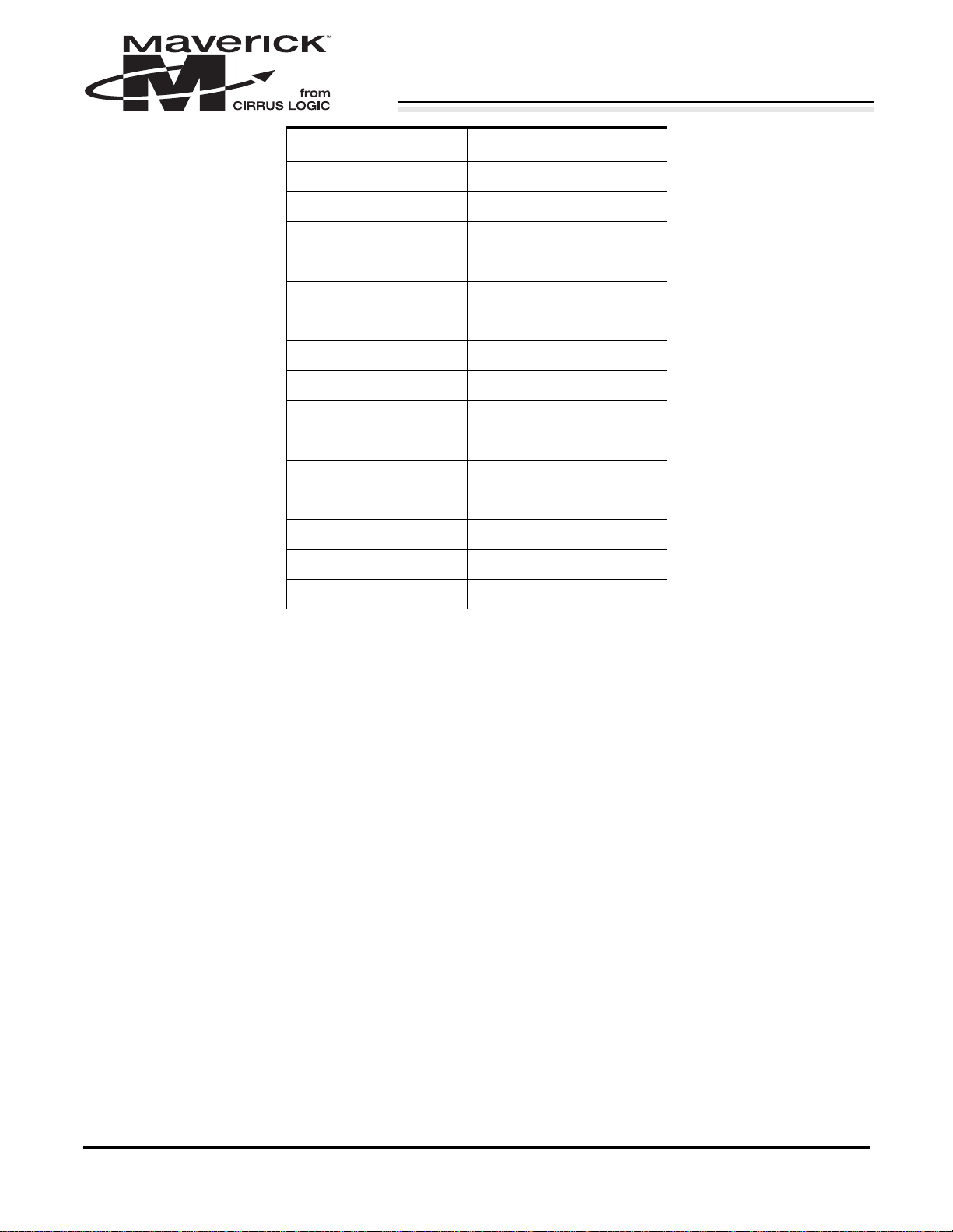
SDRAM Address Pins EP7312 Pin Names
A0
A1
A2
A3
A4
A5
A6
A7
A8
A9
A10
A11
A12
BA0
BA1
A27/DRA0
A26/DRA1
A25/DRA2
A24/DRA3
A23/DRA4
A22/DRA5
A21/DRA6
A20/DRA7
A19/DRA8
A18/DRA9
A17/DRA10
A16/DRA11
A15/DRA12
A14/DRA13
A13/DRA14
Table 14. SDRAM Address Pin Connections
2.10 SDRAM Initialization
The SDRAM is initialized in the power-on sequence as follows:
1) To stabilize internal circuits when power is applied, a 200 ms pause (or longer) must precede any signal
toggling.
2) After the pause, all banks must be precharged using the Precharge command (includes the precharge
all banks command).
3) Once the precharge is complete, and the minimum tRP is satisfied, the mode register can be programmed. After the mode register set cycle, tRSC (2 CLK minimum) pause must be satisfied as well.
(Only required for NEC SDRAM)
4) Eight or more refresh cycles must be performed.
DS508UM1 31
Page 31

2.11 CL-PS6700 PC Card Controller Interface
T wo of the expans ion memory areas are dedicated to supporting up to two CL-PS6700 PC Card controller
devices. These are selected by nCS[4] and nCS[5] (must first be enabled by bits 5 and 6 of SYSCON2).
For efficient, low power operation, both address and data are carried on the lower 16 bits of the EP7312
data bus.
Accesses are initiated by a write or r ead from the area of memory allocate d for nCS[4] or nCS[5]. The
memory map within each of these areas is segmented to allow different types of PC Card accesses to take
place, for attribute, I/O, and common memory space. The CL-PS6700 internal registers are memory
mapped within the address space as shown in Table 15.
Note: Due to the operating speed of the CL-PS6700, this interface is supported only for processor speeds of
13 and 18 MHz.
A complete description of the protocol and AC timing characteristics can be found in the CL-PS6700 data
sheet. A transaction is initiated by an access to t he nC S[4] or nCS[5] area . The chi p sel ect is a sserted, a nd
on the first clock, the upper 10 bits of the PC Card address, along with 6 bits of size, space, and slot infor-
mation are put out onto the lower 16 bits of the EP7312’ s data bus. Only word (i.e., 4-byte) and single-byte
accesses are supported, and the slot field is hardcoded to 11, since the slot field is defined as a “Reserved
field” by the CL-PS6700. The chip selects are used to select the device to be a cce ssed. The space field is
made directly from the A26 and A27 CPU address bits, according to the decode shown in Table 16 on
page 33. The size field is forced to 11 if a word access is required, or to 00 if a byte access is required. This
avoids the need to configure the interface after a reset. On the second clock cycle, the remaining 16 bits of
the PC Card address are multiplexed out onto the lower 16 bits of the data bus. If the transaction selected
is a CL-PS6700 register transaction, or a write to the PC Card (assuming there is space available in the CLPS6700’s internal write buffer) then the access will continue on the following two clock cycles. During
these following two clock cycles the upper and lower halves of the word to be read or written will be put
onto the lower 16 bits of the main data bus.
The “ptype” signal on the CL-PS6700s should be connected to the EP7312’s WRITE output pin. During
PC Card accesses, the polarity of this pin changes, and it becomes low to signify a write and high to signify
a read. It is valid with the first half word of the address. During the second half word of the address, it is
always forced high to indicate to the CL-PS6700 that the EP7312 has initiated either the write or read.
Access Type Addresses for CL-PS6700 Interface 1 Addresses for CL-PS6700 Interface 2
Attribute 0x4000.0000–0x43FFFFFF 0x5000.0000– 0x53FFFFFF
I/O 0x4400.0000–0x47FFFFFF 0x5400.0000–0x57FFFFFF
Common memory 0x4800.0000–0x4BFFFFFF 0x5800.0000–0x5BFFFFFF
CL-PS6700 registers 0x4C00.0000–0x4FFFFFFF 0x5C00.0000–0x5FFFFFFF
Table 15. CL-PS6700 Memory Map
32 DS508UM1
Page 32

Space Field Value PC CARD Memory Space
00 Attribute
01 I/O
10 Common memory
11 CL-PS6700 registers
Table 16. Space Field Decoding
The PRDY signals from each of the two CL-PS6700 devices are connected to Port B bits 0 and 1, respectively. When the PC CARD1 or PC CARD2 control bits in the SYSCON2 register are de-asserted, these
port bits are available for GPIO. When asserted, these port bits are used as the PRDY signals. When the
PRDY signal is de-asserted (i.e., low), it indicates that the CL-PS6700 is busy accessing its ca rd. If a PC
CARD access is attempted while the device is busy, the PRDY signal will cause the EP7312’s CPU to be
stalled. The EP7312’ s CPU will have to wait for the card to become available. DMA transfers to the LCD
can still continue in the background during this period of time (as described below). The EP7312 can access the registers in the CL-PS6700, regardless of the state of the PRDY signal. If the EP7312 needs to
access the PC CARD via the CL-PS6700, it waits until the PRDY signal is high before initiating a transfer
request. Once a request is sent, the PRDY signal indicates if data is available.
In the case of a PC Card write, writes can be posted to the CL-PS6700 device, with the same timing as CLPS6700 internal register writes. Writes will normally be com pleted by the CL-PS6700 device independent
of the EP7312 processor activity . If a posted write times out, or fails to complete for any other reason, then
the CL-PS6700 will issue an interrupt (i.e., a WR_FAIL interrupt). In the case where the CL-PS6700 write
buffer is already full, the PRDY signal will be de-asserted (i.e., dr iven low) and the transaction will be
stalled pending an available slot in the buf fer. In this case, the EP7312’s CPU will be stal led until the write
can be posted successfully. While the PRDY signal is de-asserted, the chip select to the CL-PS6700 will
be de-asserted and the main bus will be released so that DMA transfers to the LCD controller can continue
in the background.
In the case of a PC Card read, the PRDY signal from the CL-PS6700 will be de-asserted until the read data
is ready . At this point, it will be re asserted and the access will be complete d in the same way as for a register
access. In the case of a byte access, only one 16-bit data transfer will be required to complete the access.
While the PRDY signal is de-asserted, the chip select to the CL-PS6700 will be de-asserted, and the main
bus will be released so that DMA transfers to the LCD controller can continue in the background.
The EP7312 will re-arbitrate for control of the bus when the PRDY signal is reasserted to indicate that the
read or write transaction can be completed. The CPU will always be stalled until the PC Card access is
completed.
DS508UM1 33
Page 33

A card read operation may be split into a request cy cle and a data cycle, or it may be com bined into a single
request/data transfer cycle. This depends on whether the data requested from the card is ava ilable in the
prefetch buffer (internal to the CL-PS6700).
The request portion of the cycle, for a card read, is similar to the request phase for a card write (described
above). If the requested data is available in the prefetch buffer, the CL-PS6700 asserts the PRDY signal
before the rising edge of the third clock and the EP7312 continues the cycle to read the data. Otherwise,
the PRDY signal is de-asserted, and the request cycle is stalled. The EP7312 may then allow the DMA
address generator to gain control of the bus, to allow LCD refreshes to continue. When the CL-PS6700 is
ready with the data, it asserts the PRDY signal. The EP7312 then arbitrates for the bus and, once the re quest is granted, the suspended read cycle is resumed. The EP7312 resumes the cycle by asserting the appropriate chip select, and data is transferred on the next two clocks if a word read (one clock if a byte read).
There is no support within the EP7312 for detecting time-outs. The CL-PS6700 device must be programmed to force the cycle to be c ompl eted (with invalid dat a for a re ad) and then ge nerate a n inte rrup t if
a read or write access has timed out (i.e., RD_FAIL or WR_FAIL interrupt). The system software can then
determine which access was not successfully completed by reading the status registers within the CLPS6700.
The CL-PS6700 has support for DMA data transfers. However, DMA i s supported only by software emulation because the DMA address generator built into the EP7312 is dedicated to the LCD controller interface. If DMA is enabled within the CL-PS6700, it will assert its PDREQ signal to make a DMA request.
This can be connected to one of the EP7312’s external interrupts and be used to interrupt the CPU so that
the software can service the DMA request under program control.
Each of the CL-PS6700 devices can generate an interrupt PIRQ. Since the PIRQ signal is an open drain on
the CL-PS6700 devices, two CL-PS6700 devices may be wired OR’ed to the same interrupt. The circuit
can then be connected to one of the EP7312’s active low external interrupt sources. On the receipt of an
interrupt, the CPU can read the interrupt status registers on the CL-PS6700 devices to determine the cause
of the interrupt.
All transactions are synchronized to the EXPCLK output from the EP7312 in 18.432 MHz mode or the
external 13 MHz clock. The EXPCLK should be permanently enabled, by setting the EXCKEN bit in the
SYSCON1 register, when the CL-PS 6700 is used. The reason for this is that the PC Card interface and CLPS6700 internal write buffers need to be clocked after the EP7312 has completed its bus cycles.
A GPIO signal from the EP7312 can be connected to the PSLEEP pin of the CL-PS6700 devices to allow
them to be put into a power saving state before the EP7312 enters the Standby State. It is essential that the
software monitor the appropriate status registers within the CL-PS6700s to ensure that there are no pending posted bus transactions before the Standby State is entered. Failure to do this will result in incomplete
PC Card accesses.
34 DS508UM1
Page 34

2.12 Serial Interfaces
In addition to the two UARTs, the EP7312 offers the following serial interfaces shown in Table 17. The
inputs / outputs of three of the serial interfaces (DAI, CODEC, and SSI2) are multiplexed onto a single set
of external interface pins. If the DAISEL bit of SYSCON3 is low, then either SSI2 or the CODEC interface
will be selected to connect to the external pins. When bit 0 of SYSCON2 (SERSEL) is high, then the CODEC is connected to the external pins, when low the master / slave SSI2 is connected to these pins. When
the DAISEL bit is set high, the DAI interface is connected to the external pins. On power up, both the DAISEL and SERSEL bits are reset low , thus the master / slave SSI2 will be connected to these pins (and configured for slave mode operation to avoid external drive clashes).
The unique internal names given in Table 17 to each of the serial interfaces will be used to describe each
interface.
Pin definition information for the three multiplexed serial interfaces (SSI2, DAI, and CODEC) and the
ADC interface is described in Table 18.
Type Comments Referred To As Max. Transfer Speed
SPI / Microwire 1 Master mode only ADC Interface 128 kbits/s
SPI / Microwire 2 Master / slave mode SSI2 Interface 512 kbits/s
DAI Interface CD quality DACs and ADCs DAI Interface 1.536 Mbits/s
CODEC Interface Only for use in the PLL clock mode CODEC
Interface
Table 17. Serial Interface Options
Pin
No.
LQFP
63 SSICLK SSICLK = serial
65 SSITXFR SSKTXFR = TX
66 SSITXDA SSITXDA = TX
67 SSIRXDA SSIRXDA = RX
68 SSIRXFR SSIRXFR = RX
External
Pin Name
SSI2
Slave Mode
(Internal Name)
bit clock; Input
frame sync; Input
data; Output
data; Input
frame sync; Input
SSI2
Master
Mode
Output PCMCLK =
Output PCMSYNC = Output LRCK = Output 1
Output PCMOUT = Output SDOUT = Out-
Input PCMIN = Input SDIN = Input
Output p/u
Table 18. Serial Pin Assignments
CODEC
Internal Name
Output
(use a 10k pull-up)
64 kbits/s
DAI
Internal Name
SCLK =
Output
put
MCLK 1
Strength
1
1
DS508UM1 35
Page 35

2.13 CODEC Sound Interface
The CODEC interface allows direct connection of a telephony type CODEC to the EP7312. It provides all
the necessary clocks and timing pulses. It also performs a parallel to serial conversion or vice versa on the
data stream to or from the external CODEC device. The interface is full duplex and contains two separate
data FIFOs (16 deep by 8-bits wide, one for the receive data, another for the transmit data).
Data is transferred to or from the CODEC at 64 kbits/s. The data is either written to or read from the appropriate 16-byte FIFO. If enabled, a CODEC interrupt (CSINT) will be generated after every 8 bytes are
transferred (FIFO half full/empty). This means the interrupt rate will be every 1 msec, with a latency of
1msec.
Transmit and receive modes are enabled by asserting high both the CDENRX and CDENTX CODEC enable bits in the SYSCON1 register.
Note: Both the CDENRX and CDENTX enable bits should be asserted in tandem for data to be transmitted or
received. The reason for this is that the interrupt generation will occur 1 msec after one of the FIFOs is
enabled. For example: If the receive FIFO gets enabled first and the transmit FIFO at a later time, the
interrupt will occur 1 msec after the receive FIFO is enabled. After the first interrupt occurs, the receive FIFO
will be half full. However, it will not be possible to know how full the transmit FIFO will be since it was enabled
at a later time. Thus, it is possible to unintentionally overwrite data already in the transmit FIFO (See
Figure 5 on page 37).
After the CDENRX and CDENTX enable bits get asserted, the corresponding FIFOs become enabled.
When both FIFOs are disabled, the FIFO status flag CRXFE is set and CTXFF is cleared so that the FIFOs
appear empty. Additionally, if the CDENTX bit is low, the PCMOUT output is disabled. Asserting either
of the two enable bits causes the sync and interrupt generation logic to become active; otherwise they are
disabled to conserve power.
Data is loaded into the transmit FIFO by writing to the CODR register . At the begi nning of a transmit cycle,
this data is loaded into a shift/load register. Just prior to the byte being transferred out, PCMSYNC goes
high for one PCMCLK cycle. Then the dat a is shifted out seri ally to P CMOUT, MSB first, (with the MSB
valid at the same time PCMSYNC is asserted). Data is shifted on the rising edge of the PCMCLK output.
Receiving of data is performed by taking data in serially through PCMIN, again MSB first, shifting it
through the shift/load register and loading the complete byte into the receive F IFO. If there is no data available in the transmit FIFO, then a zero will be loaded into the shift/load register. I nput data is sampled on
the falling edge of PCMCLK. Data is read from the CODR register.
36 DS508UM1
Page 36

2.14 Endianness
The EP7312 uses a little endian configuration for internal registers. However, it is possible to connect the
device to a big endian external memory system. The big-endian / little-endian bit in the ARM720T control
register sets whether the EP7312 treats words in memory as being stored in big endian or little endian format. Memory is viewed as a linear collection of bytes numbered upwards from zero. Bytes 0 to 3 hold the
first stored word, bytes 4 to 7 the second, and so on. In the little endian scheme, the lowest numbered byte
in a word is considered to be the least significant byte of the word and the highest numbered byte is the
most significant. Byte 0 of the memory system should be connected to data lines 7 through 0 (D[7:0]) in
this scheme. In the big endian scheme the most significant byte of a word is stored at the lowest numbered
byte, and the least significant byte is stored at the highest numbered byte. Therefore, byte 0 of the memory
system should be connected to data lines 31 through 24 (D[31:24]). Load and store are the only instructions
affected by the Endianness.
Table 19 on page 38 and Table 20 on page 38 demonstrate the behavior of the EP7312 in big and little endian mode, including the effect of performing non-aligned word accesses. The register definition section
of this specification defines the behavior of the internal EP7312 registers in the big endian mode in more
detail. For further information, refer to ARM Application Note 61, Big and Little Endian Byte Addressing.
CDENRX
CDENTX
CSINT
1 ms
Interrupt occurs
Figure 5. CODEC Interrupt Timing
DS508UM1 37
1 ms
Interrupt occurs
1 ms
Interrupt occurs
Page 37

Address
(W/B)
Data in
Memory
(as seen
by the
EP7312)
Byte Lanes to Memory / Ports / Registers R0 Contents
Big Endian Memory Little Endian Memory
7:0 15:8 23:16 31:24 7:0 15:8 23: 16 31: 24 Big
Endian
Little
Endian
Word + 0 (W) 11223344 44 33 22 11 44 33 22 11 11223344 11223344
Word + 1 (W) 11223344 44 33 22 11 44 33 22 11 44112233 44112233
Word + 2 (W) 11223344 44 33 22 11 44 33 22 11 33441122 33441122
Word + 3 (W) 11223344 44 33 22 11 44 33 22 11 22334411 22334411
Word + 0 (H) 11223344 44 33 22 11 44 33 22 11 00001122 00003344
Word + 1 (H) 11223344 44 33 22 11 44 33 22 11 22000011 44000033
Word + 2 (H) 11223344 44 33 22 11 44 33 22 11 00003344 00001122
Word + 3 (H) 11223344 44 33 22 11 44 33 22 11 44000033 22000011
Word + 0 (B) 11223344 dc dc dc 11 44 dc dc dc 00000011 00000044
Word + 1 (B) 11223344 dc dc 22 dc dc 33 dc dc 00000022 00000033
Word + 2 (B) 11223344 dc 33 dc dc dc dc 22 dc 00000033 00000022
Word + 3 (B) 11223344 44 dc dc dc dc dc dc 11 00000044 00000011
NOTE: dc = don’t care
Table 19. Effect of Endianness on Read Operations
Address
(W/B)
Register
Contents
Byte Lanes to Memory / Ports / Registers
Big Endian Memory Little Endian Memory
7:0 15:8 23:16 31:24 7:0 15:8 23:16 31:24
Word + 0 (W) 11223344 44 33 22 11 44 33 22 11
Word + 1 (W) 11223344 44 33 22 11 44 33 22 11
Word + 2 (W) 11223344 44 33 22 11 44 33 22 11
Word + 3 (W) 11223344 44 33 22 11 44 33 22 11
Word + 0 (H) 11223344 44 33 44 33 44 33 44 33
Word + 1 (H) 11223344 44 33 44 33 44 33 44 33
Word + 2 (H) 11223344 44 33 44 33 44 33 44 33
Word + 3 (H) 11223344 44 33 44 33 44 33 44 33
Word + 0 (B) 11223344 44 44 44 44 44 44 44 44
Word + 1 (B) 11223344 44 44 44 44 44 44 44 44
Word + 2 (B) 11223344 44 44 44 44 44 44 44 44
Word + 3 (B) 11223344 44 44 44 44 44 44 44 44
NOTE: Bold indicates active byte lane.
Table 20. Effect of Endianness on Write Operations
38 DS508UM1
Page 38

2.15 Internal UARTs (Two) and SIR Encoder
The EP7312 contains two built-in UARTs that offers similar functionality to National Semiconductor’s
16C550A device. Both UARTs can support bit rates of up to 115.2 kbits/s and include two 16-byte FIFOs:
one for receive and one for transmit.
One of the UARTs (UART1) supports the three modem control input signals CTS, DSR, and DCD. The
additional RI input, and RTS and DTR output modem control lines are not explicitly supported but can be
implemented using GPIO ports in the EP7312. UART2 has only the RX and TX pins.
UART operation and line speeds are controlled by the UBLCR1 (UART bit rate and line control). Three
interrupts can be generated by UART1: RX, TX, and modem status interrupts. Only two can be generated
by UART2: RX and TX. The RX interrupt is asserted when the RX F IFO becomes half full or if the FIFO
is non-empty for longer than three character length times with no more characters being received. The TX
interrupt is asserted if the TX FIFO buffer reaches half empty. The modem status interrupt for UART1 is
generated if any of the modem status bits change state. Framing and parity errors are detected as each byte
is received and pushed onto the RX FIFO. An overrun error generates an RX interrupt immediately. All
error bits can be read from the 11-bit wide data register. The FIFOs can also be programmed to be one byte
depth only (i.e., like a conventional 16450 UART with double buffering).
The EP7312 also contains an IrDA (Infrared Data Association) SIR protocol encoder as a post-processing
stage on the output of UART1. This encoder can be optionally switched into the TX and RX signals of
UAR T1, so that these can be used to drive an infrared interface directly. If the SIR protocol encoder is enabled, the UART TXD1 line is held in the passive state and transitions of the RXD1 line will have no effect.
The IrDA output pin is LEDDRV, and the input from the photodiode is PHDIN. Modem status lines will
cause an interrupt (which can be masked) irrespective of whether the SIR interface is being used.
Both the UARTs operate in a similar manner to the industry standard 16C550A. When CTS is deasserted
on the UART, the UART does not stop shifting the data. It relies on software to take appropriate action in
response to the interrupt generated.
Baud rates supported for both the UARTs are dependent on frequency of operation. When operating from
the internal PLL, the interface supports various baud rates from 115.2 kbits/s downwards. The master clock
frequency is chosen so that most of the required da ta r ates are obtaina ble e xactly. When operating with a
13.0 MHz external clock source, the baud rates generated will have a slight error, which is less than or
equal to 0.75%. The rates (all measured in kbits/s) obtainable from the 13 MHz clock include: 9.6, 19.2,
38, 58, and 115.2. See UBRLCR1-2 UART1-2 Bit Rate and Line Control Registers for full details of the
available bit rates in the 13 MHz mode.
DS508UM1 39
Page 39

2.15.1 Digital Audio Interface
The DAI interface provides a high quality digital audio connection to DAI compatible audio devices. The
DAI is a subset of I2S audio format that is supported by a number of manufacturers.
The DAI interface produces one 128-bit frame at the audio sample frequency using a bit clock and frame
sync signal. Digital audio data is transferred, full duplex, via separate transmit and receive data lines. The
bit clock frequency is programmable to 64 fs or 128 fs. The sample frequency (fs) is now programmable
from 8-48 Khz using either the on-chip PLL(73.728MHz) or the external 11.2896 Mhz clock.
The DAI interfa ce contains separate transmit and receive FIFO’s. The transmit FIFO’s are 8 audio samples
deep and the receive FIFO’s are 12 audio samples deep.
DAI programming centers around the selection of the desired sample frequency (fs). The DAI shares the
same output with the CODEC and SSI as shown in Figure 6. All three clocks (MCLK, LRCK, SCLK) become a multiple of the selected sample frequency as illustrated in Figure 7 on page 42. Please see T able 22
on page 42 for the MUX programming matrix.
DAI 128/64 fs
CODEC
SSI2
Figure 6. Portion of the EP7312 Block Diagram Showing Multiplexed Feature
SSICLK, SSITXFR, SSITXDA ,
SSIRXDA
, SSIRSFR
40 DS508UM1
Page 40

2.15.1.1 DAI Operation
Following reset, the DAI logic is disabled. To enable the DAI, the applications program should first clear
the emergency underflow and overflow status bits, which are set following the reset, by writing a 1 to these
register bits (in the DAISR register). Next, the DAI control register should be programmed with the desired
mode of operation using a word write. The transmit FIFOs can either be “primed” by writing up to eight
16-bit values each, or can be filled by the normal interrupt service routine which handles the DAI FIFOs.
Finally , the FIF Os for each channel must be enabled via writes to DAIDR2. At this point, transmiss ion/reception of data begins on the transmit (SDOUT) and receive (SDIN) pins. This is synchronously controlled
by either the PLL or the external clock. These fixed frequencies pass through a programmable divider network which will create the appropriate values for SCLK, LRCLK, and MCLK for the desired sample frequency . Examples of sample frequencies are shown in Table 21. Register DAI64Fs enables/disables the bit
clock frequency of 64 fs (and the other features as shown in Figure 7 on page 42), but must be complemented by SYSCON3 bit 9 which will enable/disable 128 fs. T o enable one rate, you must disable the other.
128 fs
Audio Bit
Clock (MHz)
1.0240 0.5120 73.728 8 36 72
1.41 12 0.7056 1 1.2896 1 1.025 8 16
1.5360 0.7680 73.728 16 18 36
2.8224 1.4112 1 1.2896 22.025 4 8
3.0720 1.5360 73.728 24 12 24
4.0960 2.0480 73.728 32 9 18
5.6448 2.8224 1 1.2898 44.1 2 4
6.1440 3.0720 73.728 48 6 12
Table 21. Relationship Between Audio Clocks / Clock Sources/ Sample Frequencies
64 fs
Audio Bit Clock
(MHz)
Clock Source
(MHz)
Sample
Frequency
(KHz)
128 fs Divisor
(AUDDIV)
64 fs Divisor
(AUDDIV)
DS508UM1 41
Page 41

Programmable Divide
(AUDIV)
PLL
(73.728MHz)
EXTCLK
(11.2896)
MUX
(AUDCLKSRC)
/2
128(fs)
256Fs
/32
7-bit
counter
fixed at 4
Audio Bit Clock 128/64(fs)
DAI
BUZZ
Audio
Sample
Frequency
(fs)
MCLK
Figure 7. Di gital Audio Clock Generation
FEATURE SYSCON2 SYSCON3 DAI64 fs DAIR(DAI)
DAI –128 fs (X) DAISEL[3] (L) I2SF64[0] (L) DAIEN[16] (H)
128Fs[9] (H)
DAI-64 fs (X) DAISEL[3] (L) I2SF64[0] (H) DAIEN[16] (H)
128Fs[9] (L)
Audio
Data
FIFO
Control
SCLK
LRCLK(Fs)
BUZZ-PIN
SSI2 SERSEL[0] (L) (X) (X) DAIEN[16] (L)
CODEC SERSEL[0] (H) (X) (X) DAIEN[16] (L)
Table 22. Matrix for Programming the MUX
Abbreviations for Setting Bits
(L) = Low (Cleared)
(H) = High (Set)
(X) = Don’t care
Note: To program the MUX, you will need to do the following:
To connect the port to any of the 4 features shown above, a minimum software configuration shown in the
table above must be observed. Each register column contains the bit name (bit #) that must be cleared or
set for each feature as shown in the column. This table does not complete the programming for each of the
features, but allows access to the port only. The interrupt masks for these features will have to be
programmed as well.
2.15.1.2 DAI Frame Format
Each DAI frame is 128 bits long and it comprises one audio sample. Of this 128-bit frame, only 32 bits are
used for digital audio data. The remaining bits are output as zeros. The LRCK signal is used as a frame
synchronization signal. Each transition of LRCK delineates the left and right halves of an audio sample.
When LRCK transitions from high-to-low the next 16 bits make up the right side of an audio sample. When
LRCK transitions from low-to-high the next 16 bits make up the left side of an audio sample.
42 DS508UM1
Page 42

2.15.1.3 DAI Signals
MCLK oversampled clock. Used as an input to the EP7312 for generating the DAI timing. This sig-
nal is also usually used as an input to a DAC/ADC as an oversampled clock. This signal is
fixed at 256 times the audio sample frequency.
SCLK bit clock. Used as the bit clock input into the DAC/ADC. This signal is fixed at 128 or
64 times the audio sample frequency.
LRCK Frame sync. Used as a f rame synchroniza tion input to the DAC/ADC. This signal is fixed
at the audio sample frequency. This signal is clocked out on the negative going edge of
SCLK.
SDOUT Digital audio data out. Used for sending playback data to a DAC. This signal is clocked out
on the negative going edge of the SCLK output.
SDIN Digital audio input. Used for receiving record data from an ADC. This signal is latched by
the EP7312 on the positive going edge of SCLK.
2.15.2 ADC Interface — Master Mode Only SSI1 (Synchronous Serial Interface)
The first synchronous serial interface allows interfacing to the following peripheral devices:
• In the default mode, the device is compatible with the MAXIM MAX148/9 in external clock mode.
Similar SPI- or Microwire-compatible devices can be connected directly to the EP7312.
• In the extended mode and with negative-edge triggering selected (the ADCCON and ADCCKNSEN
bits are set, respectively, in the SYSCON3 register), this device can be interfaced to Analog Devices’
AD7811/12 chip using nADCCS as a common RFS/TFS line.
• Other features of the devices, including power management, can be utilized by software and the use of
the GPIO pins.
128 SCLKs
LRCK
SCLK
O
SDATA +3 +2 +1+5 +4-1 -2 -3 -4 -5 +3 +2 +1+5 +4-1 -2 -3 -4SDATA +3 +2 +1+5 +4-1 -2 -3 -4 -5 +3 +2 +1+5 +4-1 -2 -3 -4
SDATAI +3 +2 +1+5 +4
MSB
MSB
-1 -2 -3 -4 -5
Left Channel
LSB
LSB
MSB
MSB
-1 -2 -3 -4
RightChannel
+3 +2 +1+5 +4
LSB
LSB
Figure 8. EP7312 Rev B- Digital Audio Interface Timing – MSB / Left Justified format
DS508UM1 43
Page 43

The clock output frequency is programmable and only active during data transmissions to save power.
There are four output frequencies selectable, which will be slightly different depending whether the device
is operating in a 13 MHz mode or a 18.432 MHz–73.728 MHz mode (see T able 23). The required frequency is selected by programming the corresponding bits 16 and 17 in the SYSCON1 register. The sample
clock (SMPCLK) always runs at twice the frequency of the shift clock (ADCCLK). The output channel is
fed by an 8-bit shift register when the ADCCON bit of SYSCON3 is clear. When ADCCON is set, up to
16 bits of configuration command can be sent, as specified in the SYNCIO register. The input channel is
captured by a 16-bit shift register. The clock and synchronization pulses are activated by a write to the output shift register . During transfers the SSIBUSY (synchronous serial interface busy) bit in the system status
flags register is set. When the transfer is complete and valid data is in the 16-bit read shift register, the
SSEOTI interrupt is asserted and the SSIBUSY bit is cleared.
An additional sample clock (SMPCLK) can be enabled independently and is set at twice the transfer clock
frequency.
This interface has no local buffering capability and is only intended to be used with low bandwidth interfaces, such as for a touch-screen ADC interface.
2.15.3 Master / Slave SSI2 (Synchronous Serial Interface 2)
A second SPI / Microwire interface with full master / slave capability is provided by the EP7312 data rates
in slave mode are theoretically up to 512 kbits/s, full duplex, although continuous operation at this data
rate will give an interrupt rate of 2 kHz, which is too fast for many operating systems. This would require
a worst-case interrupt response time of less than 0.5 msec and would cause loss of data through TX underruns and RX overruns.
The interface is fully capable of being clocked at 512 kHz when in slave mode. However, it is anticipated
that external hardware will be used to frame the data into packets. T here fore, although the data w ould be
transmitted at a rate of 512 kbits/s, the sustained data rate would in fact only be 85.3 kbits/s (i.e., 1 byte
every 750 µsec). At this data rate, the required interrupt rate will be greater than 1 msec, which is acceptable.
There are separate half-word-wide RX and TX FIFOs (16 half-words each) and corresponding interrupts
which are generated when the FIFO’s are half-full or half-empty as appropriate. The inter rupts are c alled
SS2RX and SS2TX, respectively. Register SS2DR is used to access the FIFOs.
SYSCON1
bit 17
00 4.2 4
01 16.9 16
10 67.7 64
1 1 135.4 128
SYSCON1
bit 16
Table 23. ADC Interface Operation Frequencies
13.0 MHz Operation ADCCLK
Frequency (kHz)
18.432–73.728 MHz Operation
ADCCLK Frequency (kHz)
44 DS508UM1
Page 44

There are five pins to support this SSI port: SSIRXDA, SSITXFR, SSICLK, SSITXDA, and SSIRXFR.
The SSICLK, SSIRXDA, SSIRXFR, and SSITXFR signals are inputs and the SSITXDA signal is an output in slave mode. In the master mode, SSICLK, SSITXDA, SSITXFR, and SSIRXFR are outputs, and
SSIRXDA is an input. Master mode is enabled by writing a one to the SS2MAEN bit (SYSCON2[9]).
When the master / slave SSI is not required, it can be disabled to save power by writing a zero to the
SS2TXEN and the SS2RXEN bits (SYSCON2[4] [7]). When set, these two bits independently enable the
transmit and receive sides of the interface.
The master / slave SSI is synchronous, full duplex, and capable of supporting serial data transfers between
two nodes. Although the interface is byte-oriented, data is loaded in blocks of two bytes at a time. Each
data byte to be transferred is marked by a frame sync pulse, lasting one clock period, and located one clock
prior to the first bit being transferred. Direction of the SSI2 ports, in slave and master mode, is shown in
Figure 9.
Data on the link is sent MSB first and coincides with an appropriate frame sync pulse, of one clock in duration, located one clock prior to the first data bit sent (i.e., MSB). It is not possible to send data LSB first.
When operating in master mode, the clock frequency is selected to be the same as the ADC interface’s
(master mode only SSI1) — that is, the frequencies are selected by the same bits 16 and 17 of the
SYSCON1 register (i.e., the ADCKSEL bits). Thus, the maximum frequency in master mode is
128 kbits/s. The interface will support continuous transmission at this rate assuming that the OS can respond to the interrupts within 1 msec to prevent over/underruns. The timing diagram for this interface can
be found in the AC Characteristics section of this document.
Note: To allow synchronization to the incoming slave clock, the interface enable bits will not take effect until one
SSICLK cycle after they are written and the value read back from SYSCON2. The enable bits reflect the real
status of the enables internally. Hence, there will be a delay before the new value programmed to the enable
bits can be read back.
Slave EP7312
SSIRXFR
SSITXFR
SSICLK
SSIRXDA
SSITXDA
Master EP7312
SSIRXFR
SSITXFR
SSICLK
SSITXDA
SSIRXDA
Figure 9. SSI2 Port Directions in Slave and Master Mode
DS508UM1 45
Page 45

2.15.3.1 Read Back of Residual Data
All writes to the transmit FIFO must be in half-words (i.e., in units of two bytes at a time). On the receive
side, it is possible that an odd number of bytes will be received. Bytes are always loaded into the receive
FIFO in pairs. Consequently , in the case of a single residual byte remaining at the end of a transmission, it
will be necessary for the software to read the byte separately . This is done by reading the status of two b its
in the SYSFLG2 register to determine the validity of the residual data. These two bits (RESVAL, RESFRM) are both set high when a residual is valid. RESVAL is cleared on either a new transmission or on
reading of the residual bit by software. RESFRM is cleared only on a new transmission. By popping the
residual byte into the RX FIFO and then reading the status of these bits it is possible to determine if a residual bit has been correctly read.
Figure 10 illustrates this procedure. The sequenc e is as follows: re ad the RES VAL bit, if this is a 0, no a ction needs to be taken. If this is a 1, then pop the residual byte into the FIFO by writing to the SS2POP
location. Then read back the two status bits RESVAL and RESFRM. If these bits read back 01, then the
residual byte popped into the FIFO is valid and can be read back from the SS2DR register. If the bits are
not 01, then there has been another transmission received since the residual read procedure has been started. The data item that has been popped to the top of the FIFO will be invalid and should be ignored. In this
case, the correct byte will have bee n stored in the most significant b yte of the next half-word to be clocke d
into the FIFO.
Note: All the writes / reads to the FIFO are done word at a time (data on the lower 16 bits is valid and upper 16 bits
are ignored).
Software manually pops the residual byte into the RX FIFO by writing to the SS2POP location (the value
written is ignored). This write will strobe the RX FIFO write signal, causing the residual byte to be written
into the FIFO.
2.15.3.2 Support for Asymmetric Traffic
The interface supports asymmetric traffic (i.e., unbalanced data flow). This is accomplished through separate transmit and receive frame sync control lines. In operation, the receiving node receives a byte of data
on the eight clocks following the assertion of the receive frame sync control line. In a similar fashion, the
sending node can transmit a byte of data on the eight clocks following the assertion of the transmit frame
sync pulse.
Residual bit valid
00
New RX byte
received
New RX byte received
01
11
Pop FIFO
Figure 10. Residual Byte Reading
46 DS508UM1
Page 46

There is no correlation in the frequency of assertions of the RX and TX frame sync control lines (SSITXFR
and SSIRXFR). Hence, the RX path may bear a greater data throughput than the TX path, or vice versa.
Both directions, however, have an absolute maximum data throughput rate determined by the maximum
possible clock frequency, assuming that the interrupt response of the target OS is sufficiently quick.
2.15.3.3 Continuous Data Transfer
Data bytes may be sent / received in a contiguous manner without interleaving clocks between bytes. The
frame sync control line(s) are eight clocks apart and aligned with the clock representing bit D0 of the preceding byte (i.e., one bit in advance of the MSB).
2.15.3.4 Discontinuous Clock
In order to save power during the idle times, the clock line is put into a static low state. The master is responsible for putting the link into the Idle State. The Idle State will begin one clock, or more, after the last
byte transferred and will resume at least one clock prior to the first frame sync assertion. To disable the
clock, the TX section is turned off.
In Master mode, the EP7312 does not support the discontinuous clock.
2.15.3.5 Error Conditions
RX FIFO overflows are detected and conveyed via a status bit in the SYSFLG2 register. This register
should be accessed at periodic intervals by the application software. The status register should be read each
time the RX FIFO interrupts are generated. At this time the error condition (i.e., overrun flag) will indicate
that an error has occurred but cannot convey which byte contains the error. W riting to the SRXEOF register
location clears the overrun flag. TX FIFO underflow condition is detected and conveyed via a bit in the
SYSFLG2 register, which is accessed by the application software. A TX underflow error is cleared by writing data to be transmitted to the TX FIFO.
2.15.3.6 Clock Polarity
Clock polarity is fixed. TX data is presented on the bus on the rising edge of the clock. Data is latched into
the receiving device on the falling edge of the clock. The TX pin is held in a tristate condition when not
transmitting.
DS508UM1 47
Page 47

2.16 LCD Controller with Support for On-Chip Frame Buffer
The LCD controller provides all the necessary control signals to interfac e directly to a single panel multiplexed LCD. The panel size is programmable and can be any width (line length) from 32 to 1024 pixels in
16-pixel increments. The total video frame buffer size is programmable up to 128 kbytes. This equates to
a theoretical maximum panel size of 1024 x 256 pixels in 4 bits-per-pixel mode. The video frame buffer
can be located in any portion of memory controlled by the chip selects. Its start address will be fixed at
address 0x000.0000 within each chip select. The start address of the LCD video frame buffer is defined in
the FBADDR[3-0] register. These bits become the most significant nibble of the external address bus. The
default start address is 0xC000.0000 (FBADDR = 0xC). A system built using the on-chip SR AM (OCSR),
will then serve as the LCD video frame buffer and miscellaneous data store. The LCD video frame buffer
start address should be set to 0x6 in this option. Programming of the register FBADDR is only permitted
when the LCD is disabled (this is to avoid possible cycle corruption when changing the register contents
while a LCD DMA cycle is in progress). The re is no hardware protection to prevent this. It is necessary
for the software to disable the LCD controller before reprogr amming the FBADDR r egister. Full address
decoding is provided for the OCSR, up to the maximum video frame buffer size programmable into the
LCDCON register . Beyond this, the address is wrapped around. The frame buffer start address mus t not be
programmed to 0x4 or 0x5 if either CL-PS6700 interface is in use (PCMEN1 or PCMEN2 bits in the
SYSCON2 register are enabled). FBADDR should never be program med to 0x7 or 0x8, as these are the
locations for the on-chip Boot ROM and internal registers.
The screen is mapped to the video frame buffer as one contiguous block where each horizontal line of pixels is mapped to a set of consecutive bytes or words in the video RAM. The video fra me buffer can be
accessed word wide as pixel 0 is mapped to the LSB in the buffer such that the pixels are arranged in a
little endian manner.
The pixel bit rate, and hence the LCD refresh rate, can be programmed from 18.432 MHz to 576 kHz when
operating in 18.432–73.728 MHz mode, or 13 MHz to 203 kHz when operating from a 13 MHz clock. The
LCD controller is programmed by writing to the LCD control register (LCDCON). The LCDCON register
should not be reprogrammed while the LCD controller is enabled.
The LCD controller also contains two 32-bit palette registers, which allow any 4-, 2-, or 1-bit pixel value
to be mapped to any of the 15 grayscale values available. The required DMA bandwidth to support a ½
VGA panel displaying 4 bits-per-pixel data at an 80 Hz refresh rate is approximately 6.2 Mbytes/s. Assuming the frame buffer is stored in a 32-bit wide memory, the maximum theoretical bandwidth available is
86 Mbytes/s at 36.864 MHz, or 29.7 Mbytes/s at 13 MHz.
The LCD controller uses a nine stage 32-bit wide FIFO to buffer display data. The LCD controller requests
new data when there are five words remaining in the FIFO. This means that for a ½ VGA display at 4 bitsper-pixel and 80 Hz refresh rate, the maximum allowable DMA latency is approximately 3.25 µsec ((5
words x 8 bits/byte) / (640 x 240 x 4bpp x 80 Hz)) = 3.25 µs). The worst-case latency is the total number
of cycles from when the DMA request appears to when the first DMA data word actually becomes available at the FIFO. DMA has the highest priority, so it will always happen next in the system. The maximum
number of cycles required is 36 from the point at which the DMA request occurs to the point at which the
STM is complete, then another 6 cycles before the data actually arrives at the FIFO from the first DMA
read. This creates a total of 42 cycles. Assuming the frame buffer is located in 32-bit wide, the worst-case
48 DS508UM1
Page 48

latency is almost exactly 3.2 µs, with 13 MHz page mode cycles. With each cycle consuming ~77 ns (i.e.,
1/1 MHz), the value of 3.2 µs comes from 42 cycles x 77 ns/cycle = ~3.23 µs. If 16-bit wide, then the
worst-case latency will double. In this case, the maximum permissible display size will be halved, to approximately 320 x 240 pixels, assuming the same pixel depth and refresh rate has to be maintained. If the
frame buffer is to be stored in static memory , then further calculations must be performed. If 18 MHz mode
is selected, and 32-bit wide, then the worst-case la tency will be 2.26 µs (i.e., 42 cycles x 54 ns/cycle). If
36 MHz mode is selected, and 32-bit wide, then the worst-case latency drops down to 1.49 µs. This calculation is a little more complex for 36 MHz mode of operation. The total number of cycles = (12 x 4) + 7 =
55. Thus, 55 x 27 ns = ~1.49 µs.
Figure 11 shows the organization of the video map for all combinations of bits-per-pixel.
The refresh rate is not affected by the number of bits-per-pixel; however the LCD controller fetches twice
the data per refresh for 4 bits-per-pixel compared to 2 bits-per-pixel. The main reason for reducing the
number of bits-per-pixel is to reduce the power consumption of the memory where the video frame buffer
is mapped.
Pixel 1 Pixel 2 Pixel 3 Pi xel 4
Gray scale
Bit 0 Bit 1 Bit 2 Bit 3 Bit 4 Bit 5 Bit 6 Bit 7
Gray scale
4 Bits per pixel
Pixel 1 Pixel 2 Pixel 3 Pixel 4
Gray scale Gray scale
Bit 0 Bit 1 Bit 2 Bit 3 Bit 4 Bit 5 Bit 6 Bit 7
Gray scale Gray scale
2 Bits per pixel
Pixel 1 Pixel 2 Pixel 3 Pixel 4
Gray scale Gray scale
Gray scale Gray scale
Bit 0 Bit 1 Bit 2 Bit 3 Bit 4 Bit 5 Bit 6 Bit 7
1 Bit per pixel
Figure 11. Video Buffer Mapping
DS508UM1 49
Page 49

2.17 Timer Counters
Two identical timer counters are integrated into the EP7312. These are referred to as TC1 and TC2. Each
timer counter has an associated 16-bit read / write data register and some control bits in the system control
register. Each counter is loaded with the value written to the data register immediat ely . Thi s value will then
be decremented on the second active clock edge to arrive after the write (i.e., after the first complete period
of the clock). When the timer counter under flows (i.e., reaches 0), it will assert its appropriate interrupt.
The timer counters can be read at any time. The clock source and mode are selectable by writing to various
bits in the system control register . When run from the internal PLL, 512 kHz and 2 kHz rates are provided.
When using the 13 MHz external source, the default freque ncies w ill be 541 kHz and 2.115 kHz, respectively . However , only in non-PLL mode, an optional divide by 26 frequency can be generated (thus generating a 500 kHz frequency when using the 13 MHz source). This divider is enabled by setting the OSTB
(Operating System Timing Bit) in the SYSCON2 register (bit 12). When this bit is set high to select the
500 kHz mode, the 500 kHz frequency is routed to the timers instead of the 541 kHz clock. This does not
affect the frequencies derived for any of the other internal peripherals.
The timer counters can operate in two modes: free running or pre-scale.
2.17.1 Free Running Mode
In the free running mode, the counter will wrap around to 0xFFFF when it under flows and it will continue
to count down. Any value written to TC1 or TC2 will be decremented on the second edge of the selected
clock.
2.17.2 Prescale Mode
In the prescale mode, the value written to TC1 or TC2 is automatically re-loaded when the counter under
flows. Any value written to TC1 or TC2 will be decremented on the second edge of the selected clock. This
mode can be used to produce a programmable frequency to drive the buzzer (i.e., with TC1) or generate a
periodic interrupt. The formula is F=(500 kHz) / (n+1).
2.18 Real Time Clock
The EP7312 contains a 32-bit Real Time Clock (RTC). This can be written to and read from in the same
way as the timer counters, but it is 32 bits wide. The RTC is always clocked at 1 Hz, generated from the
32.768 kHz oscillator. It also contains a 32-bit output match register, this can be programmed to generate
an interrupt when the time in the RTC matches a specific time written to this register. The RTC can only
be reset by an nPOR cold reset. Because the RTC data register is updated from the 1 Hz clock derived from
the 32 kHz source, which is asynchronous to the main memory system clock, the data register should al ways be read twice to ensure a valid and stable reading. This also applies when reading back the RTCDIV
field of the SYSCON1 register, which reflects the status of the six LSBs of the RTC counter.
50 DS508UM1
Page 50

2.18.1 Characteristics of the Real Time Clock Interface
When connecting a crystal to the RTC interface pins (i.e., RTCIN and RTCOUT), the crystal and circuit
should conform to the following requirements:
• The 32.768 kHz frequency should be created by the crystals fundamental tone (i.e., it should be a fundamental mode crystal)
• A start-up resistor is not necessary, since one is provided internally.
• Start-up loading capacitors may be placed on each side of the external crystal and ground. Their value
should be in the range of 10 pF. However, their values should be selected based upon the crystal specifications. The total sum of the capacitance of the traces between the EP7312’s clock pins, the capacitors, and the crystal leads should be subtracted from the crystal’s specifications when determining the
values for the loading capacitors.
• The crystal should have a maximum 5 ppm frequency drift over the chip’s operating temperature range.
• The voltage for the crystal must be 2.5 V + 0.2 V.
Alternatively , a digital clock source can be used to drive the RTCIN pin of the EP7312. W ith this approach,
the voltage levels of the clock source should match that of the VDD supply for the EP7312’s pads (i.e., the
supply voltage level used to drive all of the non-VDD core pins on the EP7312) (i.e., RTCOUT). The output
clock pin should be left floating.
2.19 Dedicated LED Flasher
The LED flasher feature enables an external pin (PD[0] / LEDFLSH) to be toggled at a programmable rate
and duty ratio, with the intention that the external pin is connected to an LED. This module is driven from
the RTCs 32.768 kHz oscillator and works in all running modes because no CPU intervention is needed
once its rate and duty ratio have been configured (via the LEDFLSH register). The LED flash rate period
can be programmed for 1, 2, 3, or 4 seconds. The duty ratio can be programmed such that the mark portion
can be 1/16, 2/16… 16/16 of the full cycle. The external pin can provide up to 4 mA of drive current.
2.20 Two PWM Interfaces
T wo Pulse W idth Modulator (PWM) duty ratio clock outputs are provided by the EP7312. When the device
is operating from the internal PLL, the PWM will run at a frequency of 96 kHz. These signals are intended
for use as drives for external DC-to-DC converters in the Power Supply Unit (PSU) subsystem. External
input pins that would normally be connected to the output from comparators monitoring the external DCto-DC converter output are also used to enable these clocks. These are the FB[0-1] pins. The duty ratio
(and hence PWMs on time) can be programmed from 1 pulse in 16 pulses to 15 in 16. The sense of the
PWM drive signal (active high or low) is determined by latching the state of this drive signal during power
on reset (i.e., a pull-up on the drive signal will result in a active low drive output, and visa versa). This
allows either positive or negative voltages to be generated by the external DC-to-DC converter . PWMs are
disabled by writing zeros into the drive ratio fields in the PMPCON Pump Control register.
Note: To maximize power savings, the drive ratio fields should be used to disable the PWMs, instead of the FB
pins. The clocks that source the PWMs are disabled when the drive ratio fields are zeroed.
DS508UM1 51
Page 51

2.21 Boundary Scan
IEEE 1149.1 compliant JTAG is provided with the EP7312. Table 24 shows what JTAG instructions are
supported in the EP7312.
Instruction Code Description
EXTEST 0000 Places the selected
scan chain in test
mode.
SCAN_N 0010 Connects the Scan
Path Register between
TDI and TDO
SAMPLE / PRELOAD
IDCODE 1110 Connects the ID regis-
BYPASS 1111 Connects a 1-bit shift
Table 24. Instructions Supported in JTAG Mode
Note: The INTEST function will not be supported for the EP7312.
0011 NOTE: This instruc-
tion is included for
product testing only
and should ne ver be
used.
ter between TDI and
TDO
register bit TDI and
TDO
Additional user-defined instructions exist, but these are not relevant to board-level testing. For further information please refer to the ARM DDI 0087E ARM720T Data Sheet.
As there are additional scan-chains within the ARM720T processor, it is necessary to include a scan-chain
select function — shown as SCAN_N in Table 24. To select a particular scan chain, this function must be
input to the TAP controller, followed by the 4-bit scan chain identification code. The identification code
for the boundary scan chain is 0011.
Note that it is only necessary to issue the SCAN_N instruction if the device is already in the JTAG mode.
The boundary scan chain is selected as the default on test-logic reset and any of the system resets.
The contents of the device ID-register for the EP7312 are shown in Figure 12. This is equivalent to
0x0F0F.0F0F. Note this is the ID-code for the ARM720T processor.
Version Part number Manufacturer ID
00001111000011110000111100001111
Figure 12. Device ID Register
52 DS508UM1
Page 52

2.22 In-Circuit Emulation
2.22.1 Introduction
EmbeddedICE™ is an extension to the architecture of the ARM family of processors, and provides the ability to debug cores that are deeply embedded into systems. It consists of three parts:
• A set of extensions to the ARM core
• The EmbeddedICE macrocell, which provides external access to the extensions
• The EmbeddedICE interface, which provides communication between the host computer and the EmbeddedICE macrocell
The EmbeddedICE macrocell is programmed, in a serial fashion, through the TAP controller on the ARM
via the JTAG interface. The EmbeddedICE macrocell is by default disabled to mi nimize power usage, and
must be enabled at boot-up to support this functionality.
2.22.2 Functionality
The ICEBreaker module consists of two real-time watchpoint units together with a control and status register. One or both of the units can be programmed to halt the execution of the instructions by the ARM
processor. Execution is halted when either a match occurs between the values programmed into the ICEBreaker and the values currently appearing on the address bus, data bus, and the various control signals.
Any bit can be masked to remove it from the comparison. Either unit can be programmed as a watchpoint
(monitoring data accesses) or a breakpoint (monitoring instruction fetches).
Using one of these watchpoint units, an unlimited number of software breakpoints (in RAM) can be supported by substitution of the actual code.
Note: The EXTERN[1:0] signals from the ICEBreaker module are not wired out in this device. This mechanism is
used to allow watchpoints to be dependent on an external event. This behavior can be emulated in software
via the ICEBreaker control registers.
A more detailed description is available in the ARM Software Development Toolkit User Guide and Reference Manual. The ICEBreaker module and its registers are fully described in the ARM7TDMI Data Sheet.
2.23 Maximum-Configured EP7312-Based System
A maximum configured system using the EP7312 is shown in Figure 13 on page 54. This system assumes
all of the SDRAMs and ROMs are 16-bit wide devices. The keyboard may be connected to more GPIO
bits than shown to allow greater than 64 keys, however these extra pins will not be wired into the WAKEUP pin functionality.
DS508UM1 53
Page 53

CRYSTAL
CRYSTAL
PC CARD
SOCKET
CONTROLLER
×16
SDRAM
×16
SDRAM
×16
FLASH
CL-PS6700
PC CARD
×16
SDRAM
×16
SDRAM
×16
FLASH
MOSCIN
RTCIN
nCS[4]
PB0
EXPCLK
D[0-31]
A[0-27]
nMOE
WRITE
nSDRAS/
SDCAS
nSDCS[0]
SDQM[0-3]
nSDCS[1]
SDQM[0-3]
nCS[0]
nCS[1]
DD[0-3]
COL[0-7]
PA[0-7]
PB[0-7]
PD[0-7]
PE[0-2]
nPWRFL
BATOK
nEXTPWR
EP7312
nBATCHG
WAKEUP
DRIVE[0-1]
FB[0-1]
DAISSI-
SSITXFR
SSITXDA
SSIRXDA
CL1
CL2
FRM
nPOR
RUN
CLK
LCD
M
KEYBOARD
POWER
SUPPLY UNIT
DC
INPUT
AND
COMPARATORS
BATTERY
DC-TO-DC
CONVERTERS
CODEC/SSI2/
DAI
×16
FLASH
EXTERNAL MEMOR YMAPPED EXPANSION
ADDITIONAL I/O
×16
FLASH
BUFFERS
BUFFERS
AND
CS[n]
WORD
nCS[2]
nCS[3]
LEDFLSH
LATCHES
NOTE: A system can only use one of the following
peripheral interfa ces at any given time:
SSI2, CODEC, or
DAI.
Figure 13. A Maximum EP7312 Based System
LEDDRV
PHDIN
RXD1/2
TXD1/2
DSR
CTS
DCD
ADCCLK
nADCCS
ADCOUT
ADCIN
SMPCLK
IR LED AND
PHOTODIODE
2× RS-232
TRANSCEIVERS
ADC
DIGITIZER
54 DS508UM1
Page 54

2.24 I/O Buffer Characteristics
All I/O buffers on the EP7312 are CMOS threshold input bidirectional buffers except the oscillator and
power pads. For signals that are nominally inputs, the output buffer is only enabled during pin test mode.
All output buffers are three stated during system (hi-Z) test mode. All buffers have a standard CMOS
threshold input stage (apart from the Schmitt-triggered inputs) and CMOS slew-rate- controlled output
stages to reduce system noise. Table 25 defines the I/O buffer output characteristics which will apply
across the full range of temperature and voltage (i.e., these values are for 3.3 V, +70°C).
All propagation delays are specified at 50% VDD to 50% VDD, all rise times are specified as 10% VDD to
90% VDD and all fall times are specified as 90% VDD to 10% VDD.
Buffer Type Drive Current Propagation
Delay (Max)
I/O strength 1 ±4 mA 7 14 14 50 pF
I/O strength 2 ±12 mA 5 6 6 50 pF
Table 25. I/O Buffer Output Characteristics
Rise Time
(Max)
Fall Time
(Max)
Load
DS508UM1 55
Page 55

3. TEST MODES
The EP7312 supports a number of hardware activated test modes, these are activated by the pin combinations shown in Table 26. All latched signals will only alter test modes while NPOR is low, their state is
latched on the rising edge of NPOR. This allows these signals to be used normally during various test
modes.
Within each test mode, a selection of pins is used as multiplexed outputs or inputs to provide / m onitor the
test signals unique to that mode.
Test Mode Latched
nMEDCHG
Normal operation
(32-bit boot)
Normal operation
(8-bit boot)
Normal operation
(16-bit boot)
13 Mhz divided by 4 1 1 1 X 1 1
Alternative test ROM
boot
Oscillator / PLL bypass X X X X 1 0
Functional Test (EPB) 0 X X 1 0 1
Oscillator / PLL test
mode
ICE Mode X X X 1 0 0
System test (all HiZ) X X X 0 0 0
100X11
110X11
101X11
0XXX11
XXX001
Latched
PE[0]
Table 26. EP7312 Hardware Test Modes
Latched
PE[1]
Latched
nURESET
nTEST[0] nTEST[1]
3.1 Oscillator and PLL Bypass Mode
This mode is selected by nTEST[0] = 1, nTEST[1] = 0.
In this mode, all the internal oscillators and PLL are disabled, and the appropriate crystal oscillator pins
become the direct external oscillator inputs bypassing the oscillator and PLL. MOSCIN must be driven by
a 36.864 MHz clock source and RTCIN by a 32.768 kHz source.
56 DS508UM1
Page 56

3.2 Oscillator and PLL Test Mode
This mode is selected by nTEST[0] = 0, nTEST[1] = 1, Latched nURESET = 0
This test mode will enable the main oscillator and will output various buffered clock and test signals de-
rived from the main oscillator, PLL, and 32 kHz oscillator. All internal logic in the EP7312 will be static
and isolated from the oscillators, with the exception of the 6-bit ripple counter used to generate 576 kHz
and the Real Time Clock divide chain. Port A is used to drive the inputs of the PLL directly, and the various
clock and PLL outputs are monitored on the COL pins. Table 27 defines the EP7312 signal pins used in
this test mode. This mode is only intended to allow test of the oscillators and PLL. Note that these inputs
are inverted before being passed to the PLL to ensure that the default state of the port (all zero) maps onto
the correct default state of the PLL (TSEL = 1, XTALON = 1, PLLON = 1, D0 = 0, D1 = 1, PLLBP = 0).
This state will produce the correct frequencies as shown in T able 27. Any other combinations are for testing the oscillator and PLL and should not be used in-circuit.
Signal I/O Pin Function
TSEL I PA5 PLL test mode
XTLON I PA4 Enable to oscillator circuit
PLLON I PA3 Enable to PLL circuit
PLLBP I PA0 Bypasses PLL
RTCCLK O COL0 Output of RTC oscillator
CLK1 O COL1 1 Hz clock from RTC divider chain
OSC36 O COL2 36 MHz divided PLL main clock
CLK576K O COL4 576 KHz divided from above
VREF O COL6 Test clock output for PLL
Table 27. Oscillator and PLL Test Mode Signals
DS508UM1 57
Page 57

3.3 Debug / ICE Test Mode
This mode is selected by nTEST0 = 0, nTEST1 = 0, Latched nURESET = 1.
Selection of this mode enables the debug mode of the ARM720T . By default, this is dis abled which saves
approximately 3% on power.
3.4 Hi-Z (System) Test Mode
This mode selected by nTEST0 = 0, nTEST1 = 0, Latched nURESET = 0.
This test mode asynchronously disables all output buffers on the EP7312. This has the effect of removing
the EP7312 from the PCB so that other devices on the PCB can be in-circuit tested. The internal state of
the EP7312 is not altered directly by this test mode.
3.5 Software Selectable Test Functionality
When bit 11 of the SYSCON register is set high, internal peripheral bus register accesses are output on the
main address and data buses as though they were external accesses to the address space addressed by
nCS[5]. Hence, nCS[5] takes on a dual role, it will be ac tive as the strobe for internal acce sses and for any
accesses to the standard address range for nCS[5]. Additionally, in this mode, the internal signals shown
in Table 28 are multiplexed out of the device on port pins.
This test is not intended to be used when LCD DMA accesses are enabled. This is due to the fact that it is
possible to have internal peripheral bus activity simultaneously with a DMA transf er. This would cause
bus contention to occur on the external bus.
The “Waited clock to CPU” is an internally ANDed source that generates the actual CPU clock. Thus, it is
possible to know exactly when the CPU is being clocked by viewing this pin. The signals nFIQ and nIRQ
are the two output signals from the internal interrupt controller . They are input directly into the ARM720T
processor.
Signal I/O Pin Function
CLK O PE0 Waited clock to CPU
nFIQ O PE1 nFIQ interrupt to CPU
nIRQ O PE2 nIRQ interrupt to CPU
Table 28. Software Selectable Test Functionality
58 DS508UM1
Page 58

Part II: Pin and Register Reference
DS508UM1 59
Page 59

4. PIN DESCRIPTIONS
Table 29 describes the function of all external signals to the EP7312. Note that all output signals and all
I/O pins (when acting as outputs) are three stateable. This is to enable the Hi-Z test modes to be supported.
4.1 External Signal Functions
Function Signal
Name
Data bus D[0-31] I/O 32-bit system data bus for memory, SDRAM, and I/O interface
A[0-14] I/O 15 bits of system byte address during memory and expansion cycles
Address bus
A[13-27] /
DRA[0-14]
Signal Description
I/O DRA[0-14] are multiplexed with A[13-27], offering additional power
savings since the lightest loading is expected on the high order ROM
address lines.
Whenever the EP7312 is in the Standby State, the external address
and data buses are driven low. The RUN signal is used internally to
force these buses to be driven low. This is done to prevent peripherals
that are powered-down from draining current. Also, the internal periph-
eral’s signals get set to their Reset State.
Table 29. Exter nal Signal Functions
60 DS508UM1
Page 60

Function Signal
Name
BA[0-1]/
A[13-14]
nMOE/nSDCAS O ROM expansion OP enable/ SDRAM CAS control signal
nMWE/nSDWE O ROM expansion write enable/ SDRAM write enable control signal
nCS[0-3] O Chip select; active low, SRAM-like chip selects for expansion
nCS[4-5] O Chip select; active low, CS for expansion or for CL-PS6700 select
SDQM[0-3] I/O Data input/output masks
EXPRDY I Expansion port ready; external expansion devices drive this low to
Memory Inter-
face
WRITE/
nSDRAS
WORD /
HALFWORD
Signal Description
I/O SDRAM bank select pins
extend the bus cycle. This is used to insert wait states for an external
bus cycle.
O Transfer Direction/SDRAM RAS control signal
O To do write accesses of different sizes Word and Half-Word must be
externally decoded. The encoding of these signals is as follows:
Access
Size
Word 1 0
Half-Word 0 1
Byte 0 0
The core will generate an address. When doing a read, the ARM core
will select the appropriate byte channels. When doing a write, the correct bytes will have to be enabled depending on the above signals and
the least significant bits of the address bus.
The ARM architecture does not support unaligned accesses. For a
read using x 32 memory, it is assumed that you will ignore bits 1 and 0
of the address bus and perform a word read (or in power critical systems decode the relevant bits depending on the size of the access). If
an unaligned read takes place, the core will rotate the resulting data in
the register. For more information on this behavior see the LDR
instruction in the ARM7TDMI data sheet.
Table 29. External Signal Functions
Word Half-Word
(cont.)
DS508UM1 61
Page 61

Function Signal
Signal Description
Name
External Clock EXPCLK I/O Expansion clock rate is the same as the CPU clock for 13 MHz and
18 MHz. It runs at 36.864 MHz for 36,49 and 74 MHz modes; in
13 MHz mode this pin is used as the clock input.
nMEDCHG /
nBROM
I Media changed input; active low, deglitched. Used as a general pur-
pose FIQ interrupt during normal operation. It is also used on power
up to configure the processor to either boot from the internal Boot
ROM, or from external memory. When low , the chip will boot from the
Interrupts
internal Boot ROM.
nEXTFIQ I External active low fast interrupt request input
EINT[3] I External active high interrupt request input
nEINT[1-2] I Two general purpose, active low interrupt inputs
nPWRFL
I Power fail input; active low, deglitched input to force system into the
Standby State
BATOK
1
I Main battery OK input; falling edge generates a FIQ, a low level in the
Standby State inhibits system start up; deglitched input
Power
Management
nEXTPWR I External power sense; must be driven low if the system is powered by
an external source
nBATCHG
1
I New battery sense; driven low if battery voltage falls below the "no-
battery" threshold; it is a deglitched input
Table 29. External Signal Functions
(cont.)
62 DS508UM1
Page 62

Function Signal
State Control
RUN/CLKEN O This pin is programmed to either output the RUN signal or the CLKEN
WAKEUP
nURESET
SSICLK I/O DAI/CODEC/SSI2 clock signal
SSITXFR I/O DAI/CODEC/SSI2 serial data output frame/sync hronization pulse out-
DAI, CODEC
or
SSI2
Interface
SSITXDA O DAI/CODEC/SSI2 serial data output
SSIRXDA I DAI/CODEC/SSI2 serial data input
(See Table 30
on page 66 for
pin assign-
ment and
direction following multi-
plexing)
SSIRXFR I/O SSI2 serial data input frame/synchronization pulseDAI external clock
Signal Description
Name
nPOR I Power-on reset input. This signal is not deglitched. When active it
completely resets the entire system, including all the RTC registers.
Upon power-up, the signal must be held active low for a minimum of
100 µsec after V
has settled. During normal operation, nPOR needs
DD
to be held low for at least one clock cycle of the selected clock speed
(i.e., when running at 13 MHz, the pulse width of nPOR needs to be >
77 nsec).
Note that nURESET, RUN/CLKEN, TEST[0], TEST[1], PE[0], PE[1],
PE[2], DRIVE[0], DRIVE[1], DD[0], DD[1], DD[2], and DD[3] are all
latched on the rising edge of nPOR.
signal. The CLKENSL bit is used to configure this pin. When RUN is
selected, the pin will be high when the system is active or idle, low
while in the Standby State. When CLKEN is selected, the pin will only
be driven low when in the Standby State (For RUN, see Table 31 on
page 66).
1
I Wake up is a deglitched input signal. It must also be held high for at
least 125 µsec to guarantee its detection. Once detected it forces the
system into the Operating State from the Standby State. It is only
active when the system is in the Standby State. This pin is ignored
when the system is in the Idle or Operating State. It is used to wakeup
the system after first power-up, or after software has forced the system
into the Standby S t ate. WAKEUP will be ignored for up to two seconds
after nPOR goes HIGH. Therefore, the external WAKEUP logic must
be designed to allow it to rise and stay HIGH for at least 125 usec, two
seconds after nPOR goes HIGH.
1
I User reset input; active low deglitched input from user reset button.
This pin is also latched upon the rising edge of nPOR and read along
with the input pins nTEST[0-1] to force the device into special test
modes. nURESET does not reset the RTC.
put
input
Table 29. External Signal Functions
(cont.)
DS508UM1 63
Page 63

Function Signal
Name
ADCCLK O Serial clock output
ADC
Interface
(SSI1)
IrDA and
RS232
Interfaces
LCD
Keyboard &
Buzzer drive
LED Flasher
nADCCS O Chip select for ADC interface
ADCOUT O Serial data output
ADCIN I Serial data input
SMPCLK O Sample clock output
LEDDRV O Infrared LED drive output (UART1)
PHDIN I Photo diode input (UART1)
TXD[1-2] O RS232 UART1 and 2 TX outputs
RXD[1-2] I RS232 UART1 and 2 RX inputs
DSR I RS232 DSR input
DCD I RS232 DCD input
CTS I RS232 CTS input
DD[0-3] I/O LCD serial display data; pins can be used on power up to read the ID
CL[1] O LCD line clock
CL[2] O LCD pixel clock
FRM O LCD frame synchronization pulse output
COL[0-7] O Keyboard column drives (SYSCON1)
BUZ O Buzzer drive output (SYSCON1)
PD[0]/
LEDFLSH
Signal Description
of some LCD modules (See Table 31 on page 66).
M O LCD AC bias drive
O LED flasher driver — multiplexed with Port D bit 0. This pin can pro-
vide up to 4 mA of drive current.
Table 29. External Signal Functions
64 DS508UM1
(cont.)
Page 64

Function Signal
Name
PA [0-7] I/O Port A I/O (bit 6 for boot clock option, bit 7 for CL-PS6700 PRDY
General
Purpose I/O
PWM
Drives
Boundary
Scan
Test nTEST[0-1] I Test mode select inputs. These pins are used in conjunction with the
Oscillators
No Connects N/C No connects should be left as no connects; do not connect to ground
PB[0] / PRDY1
PB[1] / PRDY2
PB[2-7]
PD[0-5] I/O Port D I/O
PD[6-7]/ SDQM
[0-1]
PE[0]/
BOOTSEL[0]
PE[1] /
BOOTSEL[1]
PE[2 ]/
CLKSEL
DRIVE[0-1] I/O PWM drive outputs. These pins are inputs on power up to determine
FB[0-1] I PWM feedback inputs
TDI I JTAG data in
TDO O JTAG data out
TMS I JTAG mode select
TCLK I JTAG clock
nTRST I JTAG async reset
MOSCIN
MOSCOUT
RTCIN
RTCOUT
Signal Description
input); also used as keyboard row inputs
I/O Port B I/O. All eight Port B bits can be used as GPIOs.
When the PC CARD1 or 2 control bits in the SYSCON2 register are
de-asserted, PB[0] and PB[1] are available for GPIO. When asserted,
these port bits are used as the PRDY signals for connected CLPS6700 PC Card Host Adapter devices.
I/O Port D I/O, byte mask select.
I/O Port E I/O (3 bits only). Can be used as general purpose I/O during
normal operation.
I/O During power-on reset, PE[0] and PE[1] are inputs and are latched by
the rising edge of nPOR to select the memory width that the EP7312
will use to read from the boot code storage device (i.e., external 8-bitwide FLASH bank).
I/O During power-on reset, PE[2] is latched by the rising edge of nPOR to
select the clock mode of operation (i.e., either the PLL or external 13
MHz clock mode).
what polarity the output of the PWM should be when active. Otherwise,
these pins are always an output (See Table 31 on page 66).
power-on latched state of nURESET to select between the various
device test models.
I
Main 3.6864 MHz oscillator for 18.432 MHz–73.728 MHz PLL
O
I
Real Time Clock 32.768 kHz oscillator
O
Table 29. External Signal Functions
All deglitched inputs are via the 16.384 kHz clock. Each deglitched signal must be held active for at least
two clock periods. Therefore, the input signal must be active for at least ~125 µs to be detected cleanly.
Note: The RTC crystal must be populated for the device to function properly.
DS508UM1 65
(cont.)
Page 65

4.2 SSI / CODEC / DAI Pin Multiplexing
SSI2 CODEC DAI Direction Strength
SSICLK PCMCLK SCLK I/O 1
SSITXFR PCMSYNC LRCK I/O 1
SSITXDA PCMOUT SDOUT Output 1
SSIRXDA PCMIN SDIN Input
SSIRXFR p/u* MCLK I/O 1
* p/u = use an ~10 k pull-up
Table 30. SSI/CODEC/DAI Pin Multiplexing
The selection between SSI2 and the CODEC is controlled by the state of the SERSEL bit in SYSCON2
(See SYSCON2 System Control Register 2). The choice between the SSI2, CODEC, and the DAI is controlled by the DAISEL bit in SYSCON3 (See SYSCON3 System Control Register 3).
4.3 Output Bi-Directional Pins
RUN
Drive [0-1]
DD[0-3]
Note: The above output pins are implemented as bi-directional pins to enable the output side of the pad to be
monitored and hence provide more accurate control of timing or duration.
The RUN pin is looped back in to skew the address and data bus from each other.
Drive 0 and 1 are looped back in on power up to determine what polarity the output of the PWM should be
when active.
DD[0-3] are looped back in on power up to enable the reading of the ID of some LCD modules.
Table 31. Output Bi-Directional Pins
66 DS508UM1
Page 66

5. EP7312 MEMORY MAP
The lower 2 GByte of the address space is allocated to memory. The 0.5 GByte of address space from
0xC000.0000 to 0xDFFF .FFFF is allocated to SDRAM. The 1.5 GByte, less 8 kbytes for internal registers,
is not accessible in the EP7312. The MMU in the EP7312 should be programmed to generate an abort exception for access to this area.
Internal peripherals are addressed through a set of internal memory locations from hex address
0x8000.0000 to 0x8000.3FFF. These are known as the internal registers in the EP7312. In Table 32, the
memory map from 0x8000.0000 to 0x8000.1FFF contains registers that are compatible with the CLPS7111. These were included for backward compatibility and are referred to as old internal registers.
T able 32 also shows how the 4-Gbyte address range of the ARM720T processor (as configured within this
chip) is mapped in the EP7312. The memory map shown assumes that two CL-PS6700 PC Card controllers
are connected. If this functionality is not required, then the nCS[4] and nCS[5] memory is available. The
external boot ROM is not fully decoded (i.e., the boot code will repeat within the 256-Mbyte space from
0x7000.0000 to 0x8000.0000). See Table 11 on page 27 for the memory map when booted from on-chip
boot ROM. The SRAM is fully decoded up to a maximum size of 128 kbytes. Access to any location above
this range will be wrapped to within the range.
Address Contents Size
0xF000.0000 Reserved 256 Mbytes
0xE000.0000 Reserved 256 Mbytes
0xD000.0000 Reserved 256 Mbytes
0xC000.0000 SDRAM 64 Mbytes
0x8000.4000 Unused ~1 Gbyte
0x8000.2000
0x8000.0000
0x7000.0000 Boot ROM (nCS[7]) 128 bytes
0x6000.0000 SRAM (nCS[6]) 48 kbytes
0x5000.0000 PCMCIA-1 (nCS[5]) 4 x 64 Mbytes
0x4000.0000 PCMCIA-0 (nCS[4]) 4 x 64 Mbytes
0x3000.0000 Expansion (nCS[3]) 256 Mbytes
0x2000.0000 Expansion (nCS[2]) 256 Mbytes
0x1000.0000 ROM Bank 1 (nCS[1]) 256 Mbytes
0x0000.0000 ROM Bank 0 (nCS[0]) 256 Mbytes
Internal registers (new)
Internal registers (old)
(from CL-PS7111)
8 kbytes
8 kbytes
Table 32. EP7312 Memory Map in External Boot Mode
DS508UM1 67
Page 67

6. REGISTER DESCRIPTIONS
6.1 Internal Registers
T able 33 on page 69 shows the Internal Registers of the EP7312 that are compatible with the EP7211 when
the CPU is configured to a little endian memory system. Table 34 on page 72 shows the differences that
occur when the CPU is configured to a big endian memory system for byte-wide access to Ports A, B, and
D. All the internal registers are inherently little endian (i.e., the least significant byte is attached to bits 7
to 0 of the data bus). Hence, the system Endianness affects the addresses required for byte accesses to the
internal registers, resulting in a reversal of the byte address required to rea d / write a particular byte within
a register. Note that the internal registers have been split into two groups – the “old” and the “new”. The
old ones are the same as that used in EP7211 and are there for compatibility. The new registers are for accessing the additional functionality of the DAI interface and the LED flasher.
There is no effect on the register addresses for word accesses. Bits A[0-1] of the internal address bus are
only decoded for Ports A, B, and D (to allow read / write to individual ports). For all other registers, bits
A[0-1] are not decoded, so that byte reads will return the whole register contents onto the EP7312’ s internal
bus, from where the appropriate byte (according to the endianness) will be read by the CPU. To avoid the
additional complexity, it is preferable to perform all internal register accesses as word operations, except
for ports A to D which are explicitly designed to operate with byte a ccesses, as well as with word accesses.
An 8 k segment of memory in the range 0x8000.0000 to 0x8000.3FFF is reserved for interna l use in the
EP7312. Accesses in this range will not cause any external bus activity unless debug mode is enabled.
Writes to bits that are not explicitly defined in the internal area are legal and will have no effect. Reads
from bits not explicitly defined in the internal area are legal but will read undefined values. All the internal
addresses should only be accessed as 32-bit words and are always on a word boundary , except for the PIO
port registers, which can be accessed as bytes. Address bits in the range A[0-5] are not decoded (exc ept
for Ports A–D), this means each internal register is valid for 64 bytes (i.e., the SYSFLG1 register appears
at locations 0x8000.0140 to 0x8000.017C). There are some gaps in the register map for backward compatibility reasons, but registers located next to a gap are still only decoded for 64 bytes.
The GPIO port registers are byte-wide and can be accessed as a word but not as a half-word. These registers
additionally decode A[0-1]. All addresses are in hexadecimal notation.
Note: All byte-wide registers should be accessed as words (except Port A to Port D registers, which are designed
to work in both word and byte modes).
All registers bit alignment starts from the LSB of the register (i.e., they are all right shift justified). The
registers which interact with the 32 kHz clock or which could change during readback (i.e., RTC data
registers, SYSFLG1 register (lower 6-bits only), the TC1D and TC2D data registers, port registers, and
interrupt status registers), should be read twice and compared to ensure that a stable value has been read
back.
All internal registers in the EP7312 are reset (cleared to zero) by a system reset (i.e., nPOR, nRESET, or
nPWRFL signals becoming active), and the Real Time Clock data register (RTCDR) and match register
(RTCMR), which are only reset by nPOR becoming active. This ensures that the system time preserved
through a user reset or power fail condition. In the following register descriptions, little endian is assumed.
68 DS508UM1
Page 68

Address Name Default RD/WR Size Comments
0x8000.0000 PADR 0 RW 8 Port A data register
0x8000.0001 PBDR 0 RW 8 Port B data register
0x8000.0002 — — 8 Reserved
0x8000.0003 PDDR 0 RW 8 Port D data register
0x8000.0040 PADDR 0 RW 8 Port A data direction register
0x8000.0041 PBDDR 0 RW 8 Port B data direction register
0x8000.0042 — — 8 Reserved
0x8000.0043 PDDDR 0 RW 8 Port D data direction register
0x8000.0080 PEDR 0 RW 3 Port E data register
0x8000.00C0 PEDDR 0 RW 3 Port E data direction register
0x8000.0100 SYSCO N1 0 RW 32 System co ntrol regi ste r 1
0x8000.0140 SYSFLG1 0 RD 32 System status flags register 1
0x8000.0180 MEMCFG1 0 RW 32 Expansi on memor y co nfig ur ation re gis te r 1
0x8000.01C0 MEMCFG2 0 RW 32 Expansion memory configuration register 2
0x8000.0200 0 RW 32 Reserved
0x8000.0240 INTSR1 0 RD 32 Interrupt status register 1
0x8000.0280 INTMR1 0 RW 32 Interrupt mask register 1
0x8000.02C0 LCDCON 0 RW 32 LCD contr ol regis te r
0x8000.0300 TC1D 0 RW 16 Read / Write register sets and reads data to
TC1
0x8000.0340 TC2D 0 RW 16 Read / Write register sets and reads data to
TC2
0x8000.0380 RTCDR — RW 32 Real Time Clock data register
0x8000.03C0 RTCMR — RW 32 Real Time Clock match register
0x8000.0400 PMPCON 0 RW 12 PWM pump control register
0x8000.0440 CODR 0 RW 8 CODEC data I/O register
0x8000.0480 UARTDR1 0 RW 16 UART1 FIFO data register
0x8000.04C0 UBLCR1 0 RW 32 UART1 bit rate and line control register
0x8000.0500 SYNCIO 0 RW 32 Synchronous serial I/O data register for master
only SSI
Table 33. EP7312 Internal Registers (Little Endian Mode)
DS508UM1 69
Page 69

Address Name Default RD/WR Size Comments
0x8000.0540 PALLSW 0 RW 32 Least significant 32-bit word of LCD palette
register
0x8000.0580 PALMSW 0 RW 32 Most significant 32-bit word of LCD palette reg-
ister
0x8000.05C0 STFCLR — WR — Write to clear all start up reason flags
0x8000.0600 BLEOI — WR — Write to clear battery low interrupt
0x8000.0640 MCEOI — WR — Write to clear media changed interrupt
0x8000.0680 TEOI — WR — Write to clear tick and watchdog interrupt
0x8000.06C0 TC1EOI — WR — Write to clear TC1 interrupt
0x8000.0700 TC2EOI — WR — Write to clear TC2 interrupt
0x8000.0740 RTCEOI — WR — Write to clear RTC match interrupt
0x8000.0780 UMSEOI — WR — Write to clear UART modem status changed
interrupt
0x8000.07C0 COEOI — WR — Write to clear CODEC sound interrupt
0x8000.0800 HALT — WR — Write to enter the Idle State
0x8000.0840 STDBY — WR — Write to enter the Standby State
0x8000.0880
–
0x8000.0FFF
0x8000.1000 FB AD DR 0xC RW 4 LCD frame buffer start address
0x8000.1100 SYSCON2 0 RW 16 System co ntr ol registe r 2
0x8000.1140 SYSFLG2 0 RD 24 System status register 2
0x8000.1240 INTSR2 0 RD 16 Interrupt status register 2
0x8000.1280 INTMR2 0 RW 16 Interrupt mask register 2
0x8000.12C0
–
0x8000.147F
0x8000.1480 UARTDR2 0 RW 16 UART2 Data Register
0x8000.14C0 UBLCR2 0 RW 32 UART2 bit rate and line control register
0x8000.1500 SS2DR 0 RW 16 Master / slave SSI2 data Register
0x8000.1600 SRXEOF — WR — Write to clear RX FIFO overflow flag
0x8000.16C0 SS2POP — WR — Write to pop SSI2 residual byte into RX FIFO
Reserved Write will have no effect, read is undefined
Reserved Write will have no effect, read is undefined
Table 33. EP7312 Internal Registers (Little Endian Mode)
70 DS508UM1
(cont.)
Page 70

Address Name Default RD/WR Size Comments
0x8000.1700 KBDEOI — WR — Write to clear keyboard interrupt
0x8000.1800 Reserved — WR — Do not write to this location. A write will cause
the
processor to go into an unsupported power
savings state.
0x8000.1840
–
0x8000.1FFF
0x8000.2000 DAIR 0 RW 32 DAI control register
0x8000.2040 DAIR0 0 RW 32 DAI data register 0
0x8000.2080 DAIDR1 0 RW 32 DAI data register 1
0x8000.20C0 DAIDR2 0 WR 21 DAI data register 2
0x8000.2100 DAISR 0 RW 32 DAI status register
0x8000.2200 SYSCO N3 0 RW 16 System co ntrol regi ste r 3
0x8000.2240 INTSR3 0 RD 32 Interrupt status register 3
0x8000.2280 INTMR3 0 RW 8 Interrupt mask register 3
0x8000.22C0
0x8000.2300 SDCONF* 2 RW 32 SDRAM Configuration Register
0x8000.2340 SDRFPR* 128 RW 16 SDRAM Refresh Register
0x8000.2440 UNIQID* 0 R 32 32-bit unique ID for the EP7312 device
0x8000.2700 RANDID0* 0 R 32 Bits 31-0 of 128-bit random ID for the EP7312
Reserved — Write will have no effect, read is undefined
LEDFLSH
0 RW 7 LED Flash register
device
0x8000.2704 RANDID1* 0 R 32 Bits 63-32 of 128-bit random ID for the EP7312
device
0x8000.2708 RANDID2* 0 R 32 Bits 95-64 of 128-bit random ID for the EP7312
device
0x8000.270C RANDID3* 0 R 32 Bits 127-96 of 128-bit random ID for the
EP7312 device
0x8000.8000
BFFF.FFFF
0x8000.2600
* Internal registers that are not backward compatible with the EP72XX.
DS508UM1 71
Reserved 0 RW 32 This area contains test register used during
manufacturing test. Writes to this area should
never be attempted during normal operation as
this may cause unexpected behavior. Any read
from this register will be undefined.
DAI64Fs*
Table 33. EP7312 Internal Registers (Little Endian Mode)
0 RW 32 DAI 64Fs Control Register
(cont.)
Page 71

Big Endian
Mode
0x8000.0003 PADR 0 RW 8 Port A Data Register
0x8000.0002 PBDR 0 RW 8 Port B Data Register
0x8000.0001 — — 8 Reserved
0x8000.0000 PDDR 0 RW 8 Port D Data Register
0x8000.0043 PADDR 0 RW 8 Port A data Direction Register
0x8000.0042 PBDDR 0 RW 8 Port B Data Direction Register
0x8000.0041 — — 8 Reserved
0x8000.0040 PDDDR 0 RW 8 Port D Data Direction Register
0x0000.0080 PEDR 0 RW 3 Port E Data Register
0X8000.0000 PEDDR 0 RW 3 Port E Data Direction Register
Name Default RD/WR Size Comments
Table 34. EP7312 Internal Registers (Big Endian Mode)
All internal registers in the EP7312 are reset (cleared to zero) by a system reset (i.e., nPOR, nURESET, or
nPWRFL signals becoming active), except for the SDRAM refresh period register (DPFPR), the Real
Time Clock data register (RTCDR), and the match register (RTCMR), which are only reset by nPOR becoming active. This ensures that the SDRAM contents and s ystem time are preserved through a user reset
or power fail condition.
Note: The following Register Descriptions refer to Little Endian Mode Only
6.1.1 PADR — Port A Data Register
ADDRESS: 0x8000.0000
Values written to this 8-bit read / write register will be output on Port A pins if the corresponding data
direction bits are set high (port output). Values read from this register reflect the external state of Port
A, not necessarily the value written to it. All bits are cleared by a system reset.
6.1.2 PBDR — Port B Data Register
ADDRESS: 0x8000.0001
Values written to this 8-bit read / write register will be output on Port B pins if the corresponding data
direction bits are set high (port output). Values read from this register reflect the external state of Port
B, not necessarily the value written to it. All bits are cleared by a system reset.
72 DS508UM1
Page 72

6.1.3 PDDR — Port D Data Register
ADDRESS: 0x8000.0003
Values written to this 8-bit read / write register will be output on Port D pins if the corresponding data
direction bits are set low (port output). Values read from this register reflect the external state of Port
registers in the EP7312 are reset (cleared to zero) by a system reset (i.e., nPOR, nURESET, or nPWRFL signals becoming active), except for the SDRAM refresh period register ( S DRFPR), the Real
Time Clock data register (RTCDR), and the match register (RTCMR), which are only reset by nPOR
becoming active. This ensures that the SDRAM contents and system time are preserved through a
user reset or power fail condition.
Note: The following Register Descriptions refer to Little Endian Mode Only
6.1.4 PADDR — Port A Data Direction Register
ADDRESS: 0x8000.0040
Bits set in this 8-bit read / write register will select the corresponding pin in Port A to become an output,
clearing a bit sets the pin to input. All bits are cleared by a system reset.
6.1.5 PBDDR — Port B Data Direction Register
ADDRESS: 0x8000.0041
Bits set in this 8-bit read / write register will select the corresponding pin in Port B to become an output,
clearing a bit sets the pin to input. All bits are cleared by a system reset.
6.1.6 PDDDR — Port D Data Direction Register
ADDRESS: 0x8000.0043
Bits cleared in this 8-bit read / write register will select the corresponding pin in Port D to become an
output, setting a bit sets the pin to input. All bits are cleared by a system reset so that Port D is output
by default.
6.1.7 PEDR — Port E Data Register
ADDRESS: 0x8000.0080
Values written to this 3-bit read / write register will be output on Port E pins if the corresponding data
direction bits are set high (port output). Values read from this register reflect the external state of Port
E, not necessarily the value written to it. All bits are cleared by a system reset.
6.1.8 PEDDR — Port E Data Direction Register
ADDRESS: 0x8000.00C0
Bits set in this 3-bit read / write register will select the corresponding pin in Port E to become an output,
while the clearing bit sets the pin to input. All bits are cleared by a system reset so that Port E is input
by default.
DS508UM1 73
Page 73

6.2 System Control Registers
6.2.1 SYSCON1 — System Control Register 1
ADDRESS: 0x8000.0100
23 22 21 20 19 18
Reserved Reserved Reserved IRTXM WAKEDIS EXCKEN
17-16 15 14 13 12 11
ADCKSEL SIREN CDENRX CDENTX LCDEN DBGEN
76543-0
TC2S TC2M TC1S TC1M Keyboard scan
The system control register is a 21-bit read / write register which controls all the general configuration
of the EP7312, as well as modes etc. for peripheral devices. All bits in this register are cleared by a
system reset. The bits in the system control register SYSCON1 are defined in Table 35.
Bit Description
0-3 Keyboard scan: This 4-bit field defines the state of the keyboard column drives. The following
table defines these states.
Keyboard Scan Column
0 All driven high
1 All driven low
2–7 All high impedance (tristate)
8 Column 0 only driven high all others high impedance
9 Column 1 only driven high all others high impedance
10 Column 2 only driven high all others high impedance
11 Column 3 only driven high all others high impedance
12 Column 4 only driven high all others high impedance
13 Column 5 only driven high all others high impedance
14 Column 6 only driven high all others high impedance
15 Column 7 only driven high all others high impedance
4 TC1M: Timer counter 1 mode. Setting this bit sets TC1 to prescale mode, clearing it sets free run-
ning mode.
5 TC1S: Timer counter 1 clock source. Setting this bit sets the TC1 clock source to 512 kHz, clear-
ing it sets the clock source to 2 kHz.
6 TC2M: Timer counter 2 mode. Setting this bit sets TC2 to prescale mode, clearing it sets free run-
ning mode.
7 TC2S: Timer counter 2 clock source. Setting this bit sets the TC2 clock source to 512 kHz, clear-
ing it sets the clock source to 2 kHz.
8 UART1EN: Internal UART enable bit. Setting this bit enables the internal UART.
Table 35. SYSCON1
74 DS508UM1
Page 74

Bit Description
9 BZTOG: Bit to drive (i.e., toggle) the buzzer output directly when software mode of operation is
selected (i.e., bit BZMOD = 0). See the BZMOD and BUZFREQ (SYSCON1) bits for more
details.
10 BZMOD: This bit selects the buzzer drive mode. When BZMOD = 0, the buzzer drive output pin
is connected directly to the BZTOG bit. This is the software mode. When BZMOD = 1, the buzzer
drive is in the hardware mode. Two hardware sources are available to drive the pin. They are the
TC1 or a fixed internally generated clock source. The selection of which source is used to drive
the pin is determined by the state of the BUZFREQ bit in the SYSCON2 register. If the TC1 is
selected, then the buzzer output pin is connected to the TC1 under flow bit. The buzzer output
pin changes every time the timer wraps around. The frequency depends on what was programmed into the timer. See the description of the BUZFREQ and BZTOG bits (SYSCON2) for
more details.
11 DBGEN: Setting this bit will enable the debug mode. In this mode, all internal accesses are out-
put as if they were reads or writes to the expansion memory addressed by nCS5. nCS5 will still
be active in its standard address range. In addition, the internal interrupt request and fast interrupt request signals to the ARM720T processor are output on Port E, bits 1 and 2. Note that
these bits must be programmed to be outputs before this functionality can be observed. The
clock to the CPU is output on Port E, Bit 0 to delineate individual accesses. For example, in
debug mode:
nCS5 = nCS5 or internal I/O strobe
PE0 = CLK
PE1 = nIRQ
PE2 = nFIQ
12 LCDEN: LCD enable bit. Setting this bit enables the LCD controller.
13 CDENTX: CODEC interface enable TX bit. Setting this bit enables the CODEC interface for data
transmission to an external CODEC device.
14 CDENRX: CODEC interface enable RX bit. Setting this bit enables the CODEC interface for data
reception from an external CODEC device.
NOTE:Both CDENRX and CDENTX need to be enabled / disabled in tandem, otherwise data may
be lost.
15 SIREN: HP SIR protocol encoding enable bit. This bit will have no effect if the UART is not
enabled.
16-17 ADCKS EL: Microwire / SPI peripheral clock speed select. This two-bit field selects the frequency
of the ADC sample clock, which is twice the frequency of the synchronous serial ADC interface
clock. The table below shows the available frequencies for operation when in PLL mode. These
bits are also used to select the shift clock frequency for the SSI2 interface when set into master
mode. The frequencies obtained in 13.0 MHz mode can be found in Table 1 on page 10.
ADCKSEL ADC Sample Frequency
(kHz) — SMPCLK
00 8 4
01 32 16
10 128 64
11 256 128
Table 35. SYSCON1
(cont.)
ADC Clock Frequency
(kHz) — ADCCLK
DS508UM1 75
Page 75

Bit Description
18 EXCKEN: External expansion clock enable. If this bit is set, the EXPCLK is enabled continuously
as a free running clock with the same frequency and phase as the CPU clock, assuming that the
main oscillator is running. This bit should not be left set all the time for power consumption reasons. If the system enters the Standby State, the EXPCLK will become undefined. If this bit is
clear, EXPCLK will be active during memory cycles to expansion slots that have external wait
state generation enabled only.
19 WAKEDIS: Setting this bit disables waking up from the Standby State, via the wakeup input.
20 IRTXM: IrDA TX mode bit. This bit controls the IrDA encoding strategy. Clearing this bit means
that each zero bit transmitted is represented as a pulse of width 3/16th of the bit rate period. Setting this bit means each zero bit is represented as a pulse of width 3/16th of the period of
1 15,200-bit rate clock (i.e., 1.6 µs regardless of the selected bit rate). Setting this bit will use less
power, but will probably reduce transmission distances.
Table 35. SYSCON1
(cont.)
76 DS508UM1
Page 76

6.2.2 SYSCON2— System Control Register 2
ADDRESS: 0x8000.1100
15 14 13 12 11-10 9 8
Reserved BUZFREQ CLKENSL OSTB Reserved SS2MAEN UART2EN
7 6543210
SS2RXEN PC CARD2 PC CARD1 SS2TXEN KBWEN DRAMZ KBD6 SERSEL
The SYSCON2 register is reset to all 0s on power up.
Bit Description
0 SERSEL:The only affect of this bit is to select either SSI2 or the CODEC interface to the external
pins. See the table below for the selection options.
NOTE: If the DAISEL bit of SYSCON3 is set, then it overrides the state of the SERSEL
bit, and thus the external pins are connected to the DAI interface.
SERSEL Value Selected Serial Device to
External Pins
0 Master / slave SSI2
1CODEC
1 KBD6: The state of this bit determines how many of the Port A inputs are OR’ed together to cre-
ate the keyboard interrupt. When zero (the reset state), all eight of the Port A inputs will generate
a keyboard interrupt. When set high, only Port A bits 0 to 5 will generate an interrupt from the
keyboard. It is assumed that the keyboard row lines are connected into Port A.
2 DRAMZ: The bit determines the width of the DRAM memory interface, where: 0=32-bit DRAM
and 1=16-bit DRAM.
3 KBWEN: When the KBWEN bit is high, the EP7312 will awaken from a power saving state into
the Operating State when a high signal is on one of Port A’s inputs (irrespective of the state of the
interrupt mask register). This is called the Keyboard Direct Wakeup mode. In this mode, the interrupt request does not have to get serviced. If the interrupt is masked (i.e., the interrupt mask register 2 (INTMR2) bit 0 is low), the processor simply starts re-executing code from where it left off
before it entered the power saving state. If the interrupt is non-masked, then the processor will
service the interrupt.
4 SS2TXEN: Transmit enable for the synchronous serial interface 2. The transmit side of SSI2 will
be disabled until this bit is set. When set low, this bit also disables the SSICLK pin (to save
power) in master mode, if the receive side is low.
5 PC CARD1: Enable for the interface to the CL-PS6700 device for PC Card slot 1. The main effect
of this bit is to reassign the functionality of Port B, bit 0 to the PRDY input from the CL-PS6700
devices, and to ensure that any access to the nCS4 address space will be according to the
CL-PS6700 interface protocol.
6 PC CARD2: Enable for the interface to the CL-PS6700 device for PC Card slot 2. The main effect
of this bit is to reassign the functionality of Port B, bit 1 to the PRDY input from the CL-PS6700
devices and to ensure that any access to the nCS5 address space will be according to the
CL-PS6700 interface protocol.
Table 36. SYSCON2
DS508UM1 77
Page 77

Bit Description
7 SS2RXEN: Receive enable for the synchronous serial interface 2. The receive side of SSI2 will
be disabled until this bit is set. When both SSI2TXEN and SSI2RXEN are disabled, the SSI2
interface will be in a power saving state.
8 UART2EN: Internal UART2 enable bit. Setting this bit enables the internal UART2.
9 SS2MAEN: Master mode enable for the synchronous serial interface 2. When low, SSI2 will be
configured for slave mode operation. When high, SSI2 will be configured for master mode opera-
tion. This bit also controls the directionality of the interface pins.
12 OSTB: This bit (operating system timing bit) is for use only with the 13 MHz clock source mode.
Normally it will be set low, however when set high it will cause a 500 kHz clock to be generated
for the timers instead of the 541 kHz which would normally be available. The divider to generate
this frequency is not clocked when this bit is set low.
13 CLKENSL: CLKEN select. When low, the CLKEN signal will be output on the RUN/CLKEN pin.
When high, the RUN signal will be output on RUN/CLKEN.
14 BUZFREQ: The BUZFREQ bit is used to select which hardware source will be used as the
source to drive the buzzer output pin. When BUZFREQ = 0, the buzzer signal generated from the
on-chip timer (TC1) is output. When BUZFREQ = 1, a fixed frequency clock is output (500 Hz
when running from the PLL, 528 Hz in the 13 MHz external clock mode). See the BZMOD and
the BZTOG bits (SYSCON2) for more details.
Table 36. SYSCON2
(cont.)
78 DS508UM1
Page 78

6.2.3 SYSCON3 — System Control Register 3
ADDRESS: 0x8000.2200
15 14 13 12 11 10 9 8
Reserved Reserved Reserved Reserved Reserved ENPD67 128Fs Reserved
76543210
VERSN[2]
Reserved
Bit Description
0 ADCCON: Determines whether the ADC Configuration Extension field SYNCIO[16-31] is to be
1:2 CLKCTL[0-1]: Determines the frequency of operation of the processor / memory bus and wait
VERSN[1]
Reserved
VERSN[0]
Reserved
ADCCKNSEN DAISEL CLKCTL1 CLKCTL0 ADCCON
This register is an extension of SYSCON1 and SYSCON2, containing additional control for the
EP7312. The bits of this third system control register are defined in Table 37.
used for ADC configuration data. When this bit = 0 (default state) the ADC Configuration Byte
SYNCIO[0-7] only is used for backwards compatibility. When this bit = 1, the ADC Configuration
Extension field in the SYNCIO register is used for ADC Configuration data and the value in the
ADC Configuration Byte (SYNCIO[0-6]) selects the length of the da ta (8-bit to 16-bit).
state scaling. The table below lists the available options.
CLKCTL[1-0]
Value
Processor
Frequency
Memory Bus
Frequency
Wait State
Scaling
00 18.432 MHz 18.432 MHz 1
01 36.864 MHz 36.864 MHz 2
10 49.152 MHz 36.864 MHz 2
11 73.728 MHz 36.864 MHz 2
NOTE: To determine the number of wait states programmed refer to Table 44 on page 88 and
Table 45 on page 89. When operating at 13 MHz, the CLKCTL[0-1] bits should not be
changed from the defaul t value of ‘00’. Unde r no circumstances shoul d the CLKCTL
bits be changed using a buffered write.
3 DAISEL: When set, selects DAI interface.This action defaults to SSI (DAISEL bit is low).
4 ADCCKNSEN : When set, configuration data is transmitted on ADCOUT at the rising edge of the
ADCCLK, and data is read back on the falling edge on the ADCIN pin. When clear (default), the
opposite edges are used.
5-7 VERSN[0-2]: Additional read-only version bits — will read ‘000’
8 Reserved. This bit must be set to zero
9 128Fs: When set, this bit selects the 128 fs mode. 0 by default.
10 ENPD67: Pd[6-7] control the byte mask of the SDRAM interface. Setting of this bit allows their
use as GPIO bits as in previous devices for applications not using SDRAM.
Table 37. SYSCON3
DS508UM1 79
Page 79

6.2.4 SYSFLG1 — System Status Flags Register
ADDRESS: 0x8000.0140
31-30 29282726
VERID ID BOOTBIT1 BOOTBIT0 SSIBUSY
23 22 21-16 23 22
UTXFF1 URXFE1 RTCDIV UTXFF1 URXFE1
15 14 13 12 11
CLDFLG PFFLG RSTFLG NBFLG UBUSY1
7-4 3 2 1 0
DID WUON WUDR DCDET MCDR
The system status flags register is a 32-bit read only register, which indicates various system information. The bits in the system status flags register SYSFLG1 are defined in Table 38.
Bit Description
0 MCDR: Media changed direct read. This bit reflects the INVERTED non-latched status of the
media changed input.
1 DCDET: This bit will be set if a non-battery operated power supply is powering the system (it is
the inverted state of the nEXTPWR input pin).
2 WUDR: Wake up direct read. This bit reflects the non-latched state of the wakeup signal.
3 WUON: This bit will be set if the system has been brought out of the Standby State by a rising
edge on the wakeup signal. It is cleared by a system reset or by writing to the HALT or STDBY
locations.
4-7 DID: Display ID nibble. This 4-bit nibble reflects the latched state of the four LCD data lines. The
state of the four LCD data lines is latched by the LCDEN bit, and so it will always reflect the last
state of these lines before the LCD controller was enabled.
8 CTS: This bit reflects the current status of the clear to send (CTS) modem control input to
UART1.
9 DSR: This bit reflects the current status of the data set ready (DSR) modem control input to
UART1.
10 DCD: This bit reflects the current status of the data carrier detect (DCD) modem control input to
UART1.
11 UBUSY1: UART1 transmitter busy. This bit is set while UART1 is busy transmitting data, it is
guaranteed to remain set until the complete byte has been sent, including all stop bits.
12 NBFLG: New battery flag. This bit will be set if a low to high transition has occurred on the
nBA TCHG input, it is cleared by writing to the STFCLR location.
13 RSTFLG: Reset flag. This bit will be set if the RESET button has been pressed, forcing the
nURESET input low. It is cleared by writing to the STFCLR location.
14 PFFLG: Power Fail Flag. This bit will be set if the system has been reset by the nPWRFL input
pin, it is cleared by writing to the STFCLR location.
15 CLDFLG: Cold start flag. This bit will be set if the EP7312 has been reset with a power on reset,
it is cleared by writing to the STFCLR location.
Table 38. SYSFLG1
80 DS508UM1
Page 80

Bit Description
16-21 RTCDIV: This 6-bit field reflects the number of 64 Hz ticks that have passed since the last incre-
ment of the RTC. It is the output of the divide by 64 chain that divides the 64 Hz tick clock down
to 1 Hz for the RTC. The MSB is the 32 Hz output, the LSB is the 1 Hz output.
22 URXFE1: UART1 receiver FIFO empty. The meaning of this bit depends on the state of the UFI-
FOEN bit in the UART1 bit rate and line control register. If the FIFO is disabled, this bit will be set
when the RX holding register is empty. If the FIFO is enabled, the URXFE bit will be set when the
RX FIFO is empty.
23 UTXFF1: UART1 transmit FIFO full. The meaning of this bit depends on the state of the UFI-
FOEN bit in the UART1 bit rate and line control register. If the FIFO is disabled, this bit will be set
when the TX holding register is full. If the FIFO is enabled, the UTXFF bit will be set when the TX
FIFO is full.
24 CRXFE: CODEC RX FIFO empty bit. This will be set if the 16-byte CODEC RX FIFO is empty.
25 CTXFF: CODEC TX FIFO full bit. This will be set if the 16-byte CODEC TX FIFO is full.
26 SSIBUSY: Synchronous serial interface busy bit. This bit will be set while data is being shifted in
or out of the synchronous serial interface, when clear data is valid to read.
27-28 BOOTBIT[0-1]: These bits indicate the default (power-on reset) bus width of the ROM interface.
See
Memory Configuration Registers
of these bits reflect the state of Port E[0-1] during power on reset, as shown in the table below.
for more details on the ROM interface bus width. The state
PE[1]
(BOOTBIT1)
0 0 32-bit
0 1 8-bit
1 0 16-bit
11Reserved
29 ID: Will always read “1” for the EP7312 device
30-31 VERID: Version ID bits. These 2 bits determine the version ID for the EP7312. Will read “01” for
the initial version.
Table 38. SYSFLG1
PE[0]
(BOOTBIT0)
(cont.)
Boot Option
DS508UM1 81
Page 81

6.2.5 SYSFLG2 — System Status Register 2
ADDRESS: 0x8000.1140
23 22 21-12 11 10-7 6
UTXFF2 URXFE2 Reserved UBUSY2 Reserved CKMODE
543210
SS2TXUF SS2TXFF SS2RXFE RESFRM RESVAL SS2RXOF
The bits of the second system status register are defined in Table 39.
Bit Description
0 SS2RXOF: Master / slave SSI2 RX FIFO overflow. This bit is set when a write is attempted to a
full RX FIFO (i.e., when RX is still receiving data and the FIFO is full). This can be cleared in one
of two ways:
1. Empty the FIFO (remove data from FIFO) and then write to SRXEOF location.
2. Disable the RX (affects of disabling the RX will not take place until a full SSI2 clock
cycle after it is disabled)
1 RESVAL: Master / slave SSI2 RX FIFO residual byte present, cleared by popping the residual
byte into the SSI2 RX FIFO or by a new RX frame sync pulse.
2 RESFRM: Master / slave SSI2 RX FIFO residual byte present, cleared only by a new RX frame
sync pulse.
3 SS2RXFE: Master / slave SSI2 RX FIFO empty bit. This will be set if the 16 x 16 RX FIFO is
empty.
4 SS2TXFF: Master / slave SSI2 TX FIFO full bit. This will be set if the 16 x 16 TX FIFO is full. This
will get cleared when data is removed from the FIFO or the EP7312 is reset.
5 SS2TXUF: Master / slave SSI2 TX FIFO Underflow bit. This will be set if there is attempt to trans-
mit when TX FIFO is empty. This will be cleared when FIFO gets loaded with data.
6 CKMODE: This bit reflects the status of the CLKSEL (PE[2]) input, latched during nPOR. When
low, the PLL is running and the chip is operating in 18.432–73.728 MHz mode. When high the
chip is operating from an external 13 MHz clock.
11 UBUSY2: UART2 transmitter busy. This bit is set while UART2 is busy transmitting data; it is
guaranteed to remain set until the complete byte has been sent, including all stop bits.
22 URXFE2: UART2 receiver FIFO empty. The meaning of this bit depends on the state of the UFI-
FOEN bit in the UART2 bit rate and line control register. If the FIFO is disabled, this bit will be set
when the RX holding register contains is empty. If the FIFO is enabled, the URXFE bit will be set
when the RX FIFO is empty.
23 UTXFF2: UART2 transmit FIFO full. The meaning of this bit depends on the state of the UFI-
FOEN bit in the UART2 bit rate and line control register. If the FIFO is disabled, this bit will be set
when the TX holding register is full. If the FIFO is enabled, the UTXFF bit will be set when the TX
FIFO is full.
Table 39. SYSFLG2
82 DS508UM1
Page 82

6.3 Interrupt Registers
6.3.1 INTSR1 — Interrupt Status Register 1
ADDRESS: 0x8000.0240
15 14 13 12 11 10 9 8
SSEOTI UMSINT URXINT1 UTXINT1 TINT RTCMI TC2OI TC1OI
7 6543210
EINT3 EINT2 EINT1 CSINT
The interrupt status register is a 32-bit read only register. The interrupt status register reflects the current state of the first 16 interrupt sources within the EP7312. Each bit is set if the appropriate interrupt
is active. The interrupt assignment is given in Table 40.
Bit Description
0 EXTFIQ: External fast interrupt. This interrupt will be active if the nEXTFIQ input pin is forced low and is
mapped to the FIQ input on the ARM720T processor.
1 BLINT: Battery low interrupt. This interrupt will be active if no external supply is present (nEXTPWR is
high) and the battery OK input pin BATOK is forced low. This interrupt is de-glitched with a 16 kHz clock,
so it will only generate an interrupt if it is active for longer than 125 µsec. It is mapped to the FIQ input
on the ARM720T processor and is cleared by writing to the BLEOI location.
NOTE: BLINT is disabled during the Standby State.
2 WEINT: Tick Watch dog expired interrupt. This interrupt will become active on a rising edge of the peri-
odic 64 Hz tick interrupt clock if the tick interrupt is still active (i.e., if a tick interrupt has not been serviced for a complete tick period). It is mapped to the FIQ input on the ARM720T processor and the TEOI
location.
NOTE: WEINT is disabled during the Standby State.
Watch dog timer tick rate is 64 Hz (in 13 MHz and 73.728–18.432 MHz modes).
Watchdog timer is turned off during the Standby State.
3 MCINT: Media changed interrupt. This interrupt will be active after a rising edge on the nMEDCHG input
pin has been detected, This input is de-glitched with a 16 kHz clock so it will only generate an interrupt
if it is active for longer than 125 µsec. It is mapped to the FIQ input on the ARM7TDMI processor and is
cleared by writing to the MCEOI location. On power-up, the Media change pin (nMEDCHG) is used as
an input to force the processor to either boot from the internal Boot ROM, or from external memory.
After power-up, the pin can be used as a general purpose FIQ interrupt pin.
4 CSINT: CODEC sound interrupt, generated when the data FIFO has reached half full or empty (depend-
ing on the interface direction). It is cleared by writing to the COEOI location.
5 EINT1: External interrupt input 1. This interrupt will be active if the nEINT1 input is active (low). It is
cleared by returning nEINT1 to the passive (high) state.
6 EINT2: External interrupt input 2. This interrupt will be active if the nEINT2 input is active (low). It is
cleared by returning nEINT2 to the passive (high) state.
7 EINT3: External interrupt input 3. This interrupt will be active if the EINT3 input is active (high). It is
cleared by returning EINT3 to the passive (low) state.
8 TC1OI: TC1 under flow interrupt. This interrupt becomes active on the next falling edge of the timer
counter 1 clock after the timer counter has under flowed (reached zero). It is cleared by writing to the
TC1EOI location.
MCINT WEINT BLINT EXTFIQ
Table 40. INTSR1
DS508UM1 83
Page 83

Bit Description
9 TC2OI: TC2 under flow interrupt. This interrupt becomes active on the next falling edge of the timer
counter 2 clock after the timer counter has under flowed (reached zero). It is cleared by writing to the
TC2EOI location.
10 RTCMI: RTC compare match interrupt. This interrupt becomes active on the next rising edge of the
1 Hz Real Time Clock (one second later) after the 32-bit time written to the Real Time Clock match register exactly matches the current time in the RTC. It is cleared by writing to the RTCEOI location.
11 TINT: 64 Hz tick interrupt. This interrupt becomes active on every rising edge of the internal
64 Hz clock signal. This 64 Hz clock is derived from the 15-stage ripple counter that divides the
32.768 kHz oscillator input down to 1 Hz for the Real Time Clock. This interrupt is cleared by writing to
the TEOI location.
NOTE: TINT is disabled / turned off during the Standby State.
12 UTXINT1: Internal UART1 transmit FIFO half-empty interrupt. The function of this interrupt source
depends on whether the UART1 FIFO is enabled. If the FIFO is disabled (FIFOEN bit is clear in the
UART1 bit rate and line control register), this interrupt will be active when there is no data in the UART1
TX data holding register and be cleared by writing to the UART1 data register. If the FIFO is enabled
this interrupt will be active when the UART1 TX FIFO is half or more empty, and is cleared by filling the
FIFO to at least half full.
13 URXINT1: Internal UART1 receive FIFO half full interrupt. The function of this interrupt source depends
on whether the UART1 FIFO is enabled. If the FIFO is disabled this interrupt will be active when there is
valid RX data in the UART1 RX data holding register and be cleared by reading this data. If the FIFO is
enabled this interrupt will be active when the UART1 RX FIFO is half or more full or if the FIFO is non
empty and no more characters have been received for a three character time out period. It is cleared by
reading all the data from the RX FIFO.
14 UMSINT: Internal UART1 modem status changed interrupt. This interrupt will be active if either of the
two modem status lines (CTS or DSR) change state. It is cleared by writing to the UMSEOI location.
15 SSEOTI: Synchronous serial interface end of transfer interrupt. This interrupt will be active after a com-
plete data transfer to and from the external ADC has been completed. It is cleared by reading the ADC
data from the SYNCIO register.
Table 40. INTSR1
(cont.)
6.3.2 INTMR1 — Interrupt Mask Register 1
ADDRESS: 0x8000.0280
15 14 13 12 11 10 9 8
SSEOTI UMSINT URXINT UTXINT TINT RTCMI TC2OI TC1OI
7 6543210
EINT3 EINT2 EINT1 CSINT
This interrupt mask register is a 32-bit read / write register, which is used to selectively enable any of
the first 16 interrupt sources within the EP7312. The four shaded interrupts all generate a fast interrupt
request to the ARM720T processor (FIQ), this will cause a jump to processor virtual address
0000.001C. All other interrupts will generate a standard interrupt request (IRQ), this will cause a jump
to processor virtual address 0000.0018. Setting the appropriate bit in this register enables the corresponding interrupt. All bits are cleared by a system reset. Please refer to
Register 1
for individual bit details.
84 DS508UM1
MCINT WEINT BLINT EXTFIQ
INTSR1 Interrupt Status
Page 84

6.3.3 INTSR2 — Interrupt Status Register 2
ADDRESS: 0x8000.1240
15-14 13 12 11-3 2 1 0
Reserved URXINT2 UTXINT2 Reserved SS2TX SS2RX KBDINT
The interrupt status register also reflects the current state of the new interrupt sources within the
EP7312. Each bit is set if the appropriate interrupt is active. The interrupt assignment is given in
Table 41.
Bit Description
0 KBDINT: Keyboard interrupt. This interrupt is generated whenever a key is pressed, from the log-
ical OR of the first 6 or all 8 of the Port A inputs (depending on the state of the KBD6 bit in the
SYSCON2 register. The interrupt request is latched and can be de-asserted by writing to the
KBDEOI location.
NOTE: KBDINT is not deglitched.
1 SS2RX: Synchronous serial interface 2 receives FIFO half or greater full interrupt. This is gener-
ated when RX FIFO contains 8 or more half-words. This interrupt is cleared only when the RX
FIFO is emptied or one SSI2 clock after RX is disabled.
2 SS2TX: Synchronous serial interface 2 transmit FIFO less than half empty interrupt. This is gen-
erated when TX FIFO contains fewer than 8 byte pairs. This interrupt gets cleared by loading the
FIFO with more data or disabling the TX. One synchronization clock required when disabling the
TX side before it takes effect.
12 UTXINT2: UART2 transmit FIFO half empty interrupt. The function of this interrupt source
depends on whether the UART2 FIFO is enabled. If the FIFO is disabled (FIFOEN bit is clear in
the UART2 bit rate and line control register), this interrupt will be active when there is no data in
the UART2 TX data holding register and be cleared by writing to the UART2 data register. If the
FIFO is enabled, this interrupt will be active when the UART2 TX FIFO is half or more empty and
is cleared by filling the FIFO to at least half full.
13 URXINT2: UART2 receive FIFO half full interrupt. The function of this interrupt source depends
on whether the UART2 FIFO is enabled. If the FIFO is disabled, this interrupt will be active when
there is valid RX data in the UART2 RX data holding register and be cleared by reading this data.
If the FIFO is enabled, this interrupt will be active when the UART2 RX FIFO is half or more full or
if the FIFO is non-empty, and no more characters have been received for a three-character time-
out period, t is cleared by reading all the data from the RX FIFO.
Table 41. INSTR2
6.3.4 INTMR2 — Interrupt Mask Register 2
ADDRESS: 0x8000.1280
15-14 13 12 11-3 2 1 0
Reserved URXINT2 UTXINT2 Reserved SS2TX SS2RX KBDINT
Please refer to INTSR2 for individual bit details.
DS508UM1 85
Page 85

6.3.5 INTSR3 — Interrupt Status Register 3
ADDRESS: 0x8000.2240
7-1 0
Reserved DAIINT
Each bit is set if the appropriate interrupt is active. The interrupt assignment is given in Table 42 on
page 86.
Bit Description
0 DAIINT: DAI interface interrupt. The cause must be determined by reading the DAI status regis-
ter. It is mapped to the FIQ interrupt on the ARM720T processor
Table 42. INTSR3
6.3.6 INTMR3 — Interrupt Mask Register 3
ADDRESS: 0x8000.2280
7-1 0
Reserved DAIINT
This register is an extension of INTMR1 and INTMR2, containing interrupt mask bits for the EP7312.
Please refer to INTSR3 for individual bit details.
6.4 Memory Configuration Registers
6.4.1 MEMCFG1 — Memory Configuration Register 1
ADDRESS: 0x8000.0180
31-24 23-16 15-8 7-0
nCS[3] configuration nCS[2] configuration nCS[1] configuration nCS[0] configuration
Expansion and ROM space is selected by one of eight chip selects. One of the chip selects (nCS[6])
is used internally for the on-chip SRAM, and the configuration is hardwired for 32-bit-wide, minimumwait-state operation. nCS[7] is used for the on-chip Boot ROM and the configuration field is hardwired
for 8-bit-wide, minimum-wait-state operation. Data written to the configuration fields for either nCS[6]
or nCS7 will be ignored. Two of the chip selects (nCS[4-5]) can be used to access two CL-PS6700
PC CARD controller devices, and when either of these interfaces is enabled, the configuration field
for the appropriate chip select in the MEMCFG2 register is ignored. When the PC CARD1 or 2 control
bit in the SYSCON2 register is disabled, then nCS[4] and nCS[5] are active as normal and can be
programmed using the relevant fields of MEMCFG2, as for the other four chip selects. All of the six
external chip selects are active for 256 Mbytes and the timing and bus transfer width can be programmed individually. This is accomplished by programming the six-byte-wide fields contained in two
32-bit registers, MEMCFG1 and MEMCFG2. All bits in these registers are cleared by a system reset
(except for the nCS[6] and nCS[7] configurations).
The Memory Configuration Register 1 is a 32-bit read / write register which sets the configuration of
the four expansion and ROM selects nCS[0-3]. Each select is configured with a 1-byte field starting
with expansion select 0.
86 DS508UM1
Page 86

6.4.2 MEMCFG2 — Memory Configuration Register 2
ADDRESS: 0x8000.01C0
31-24 23-16 15-8 7-0
(Boot ROM) (Local SRAM) nCS[5] configuration nCS[4] configuration
76 5-2 1-0
CLKENB SQAEN Wait States Field Bus width
The Memory Configuration Register 2 is a 32-bit read / write register which sets the configuration of
the two expansion and ROM selects nCS[4-5]. Each select is configured with a 1-byte field starting
with expansion select 4.
Each of the six non-reserved byte fields for chip select configuration in the memory configuration registers are identical and define the number of wait states, the bus width, enable EXPCLK output during
accesses and enable sequential mode access. This byte field is defined below. This arrangement applies to nCS[0-3], and nCS[4-5] when the PC CARD enable bits in the SYSCON2 register are not set.
The state of these bits is ignored for the Boot ROM and local SRAM fields in the MEMCFG2 register.
Table 43 on page 88 defines the bus width field. Note that the effect of this field is dependent on the
two BOOTBIT bits that can be read in the SYSFLG1 register. All bits in the memory configuration register are cleared by a system reset, and the state of the BOOTBIT bits are determined by Port E bits
0 and 1 on the EP7312 during power-on reset. The state of PE[1] and PE[0] determine whether the
EP7312 is going to boot from either 32-bit-wide, 16-bit-wide or 8-bit-wide ROMs.
Table 44 on page 88 shows the values for the wait states for random and sequential wait states at 13
and 18 MHz bus rates. At 36 MHz bus rate, the encoding becomes more complex. Table 45 on
page 89 preserves compatibility with the previous devices, while allowing the previously unused bit
combinations to specify more variations of random and sequential wait states.
DS508UM1 87
Page 87

Bus Width
Field
00 0 0 32-bit wide bus access Low, Low
01 0 0 16-bit wide bus access Low, Low
10 0 0 8-bit wide bus access Low, Low
11 0 0 Reserved Low, Low
00 0 1 8-bit wide bus access Low, High
01 0 1 Reserved Low, High
10 0 1 32-bit wide bus access Low, High
11 0 1 16-bit wide bus access Low, High
00 1 0 16-bit wide bus access High, Low
01 1 0 32-bit wide bus access High, Low
10 1 0 Reserved High, Low
11 1 0 8-bit wide bus access High, Low
BOOTBIT1 BOOTBIT0 Expansion Transfer
Mode
Table 43. Valu es of the Bus Width Field
Port E bits 1,0 during
NPOR reset
Value No. of Wait States
Random
00 4 3
01 3 2
10 2 1
11 1 0
Table 44. Values of the Wait State Field at 13 MHz and 18 MHz
No. of Wait States
Sequential
88 DS508UM1
Page 88

Bit 3 Bit 2 Bit 1 Bit 0
0 000 8 3
0 001 7 3
0 010 6 3
0 011 5 3
0 100 4 2
0 101 3 2
0 110 2 2
0 111 1 2
1 000 8 1
1 001 7 1
1 010 6 1
1 011 5 1
1 100 4 0
1 101 3 0
1 110 2 0
Wait States
Random
Wait States
Sequential
1 111 1 0
Table 45. Values of the Wait State Field at 36 MHz
Bit Description
6 SQAEN: Sequential access enable. Setting this bit will enable sequential accesses that are on a
quad word boundary to take advantage of faster access times from devices that support page
mode. The sequential access will be faulted after four words (to allow video refresh cycles to
occur), even if the access is part of a longer sequential access. In addition, when this bit is not
set, non-sequential accesses will have a single idle cycle inserted at least every four cycles so
that the chip select is de-asserted periodically between accesses for easier debug.
7 CLKENB: Expansion clock enable. Setting this bit enables the EXPCLK to be active during
accesses to the selected expansion device. This will provide a timing reference for devices that
need to extend bus cycles using the EXPRDY input. Back-to-back (but not necessarily page
mode) accesses will result in a continuous clock. This bit will only affect EXPCLK when the PLL
is being used (i.e., in 73.728–18.432 MHz mode). When operating in 13 MHz mode, the EXPCLK
pin is an input, so it is not affected by this register bit. To save power internally, it should always
be set to zero when operating in 13 MHz mode.
Table 46. MEMCFG2
DS508UM1 89
Page 89

See the “AC Electrical Specification” section in the
The memory area decoded by CS[6] is reserved for the on-chip SRAM, hence this does not require
a configuration field in MEMCFG2. It is automatically set up for 32-bit-wide, no-wait-state accesses.
For the Boot ROM, it is automatically set up for 8-bit, no wait state accesses.
Chip selects nCS[4] and nCS[5] are used to select two CL-PS6700 PC CARD controller devices.
These have a multiplexed 16-bit wide address / data interface, and the configuration bytes in the
MEMCFG2 register have no meaning when these interfaces are enabled.
6.5 Timer / Counter Registers
6.5.1 TC1D — Timer Counter 1 Data Register
ADDRESS: 0x8000.0300
The timer counter 1 data register is a 16-bit read / write register which sets and reads data to TC1.
Any value written will be decremented on the next rising edge of the clock.
6.5.2 TC2D — Timer Counter 2 Data Register
ADDRESS: 0x8000.0340
The timer counter 2 data register is a 16-bit read / write register which sets and reads data to TC2.
Any value written will be decremented on the next rising edge of the clock.
6.5.3 RTCDR — Real Time Clock Data Register
EP7312 Data Sheet
for more details on bus timing.
ADDRESS: 0x8000.0380
The Real Time Clock data register is a 32-bit read / write register, which sets and reads the binary
time in the RTC. Any value written will be incremented on the next rising edge of the 1 Hz clock. This
register is reset only by nPOR.
6.5.4 RTCMR — Real Time Clock Match Register
ADDRESS: 0x8000.03C0
The Real Time Clock match register is a 32-bit read / write register, which sets and reads the binary
match time to RTC. Any value written will be compared to the current binary time in the RTC, if they
match it will assert the RTCMI interrupt source. This register is reset only by nPOR.
6.6 LEDFLSH Register
ADDRESS: 0x8000.22C0
6 5-2 1-0
Enable Duty ratio Flash rate
The output is enabled whenever LEDFLSH[6] = 1. When enabled, PDDDR[0] needs to be configured
as an output pin and the bit cleared to ‘0’ (See
the LED Flasher is disabled, the pin defaults to being used as Port D bit 0. Thus, this will ensure that
the LED will be off when disabled.
“PDDDR — Port D Data Direction Register”
.) When
90 DS508UM1
Page 90

The flash rate is determined by the LEDFLSH[0-1] bits, in the following way:
LEDFLSH[0-1] Flash Period (sec)
00 1
01 2
10 3
11 4
Table 47. LED Flash Rates
LEDFLSH[2-5] Duty Ratio
(time on: time off)
0000 01:15 1000 09:07
0001 02:14 1001 10:06
0010 03:13 1010 11:05
0011 04:12 1011 12:04
0100 05:11 1100 13:03
0101 06:10 1101 14:02
0110 07:09 1110 15:01
0111 08:08 1111 16:00 (continually on)
Table 48. LED Duty Ratio
LEDFLSH[2-5] Duty Ratio
(time on: time off)
6.7 SDCONF — SDRAM Control Register
ADDRESS: 0x8000.2300
31-11 10 9 8-7 6-5 4-2 1-0
Reserved SDACTIVE CLKCTL SDWIDTH SDSIZE Reserved CASLAT
Bit Description
0-1 How many clock cycles after CAS before the device is ready for reading or writing. ‘00’ =>
Reserved, ‘01’ => Reserved, ‘10’ => CAS Latency = 2, ‘11’ => CAS Latency = 3. The default
value is ‘10’ for CAS latency = 2.
2-4 Reserved
5-6 The capacity of each SDRAM. The values are: ‘00’=>16Mits, ‘01’=>64Mbits, ‘10’=>128Mbits,
‘11’=>256Mbits
7-8 The width of each SDRAM. ‘00’=>4bits, ‘01’=>8bits, ‘10’=>16 bits, ‘11’=>32 bits
DS508UM1 91
Page 91

Bit Description
9 Control over the SDRAM clock. ‘0’=> SDRAM clock is permanently enabled except when in
standby mode. ‘1’=>SDRAM clock stops when the EP7312 is put into inactive mode i.e., SDACTIVE = ‘0’, or when EP7312 is in standby mode.
10 Enables the SDRAM controller: ‘0’ disables, ‘1’ enables. The SDRAM controller will only initialize
if SDACTIVE is set to 1. After initialization, resetting this parameter will cause the SDRAM controller to enter an inactive state. It will remain in this state until SDACTIVE is set to 1.
11-31 Reserved
6.8 SDRFPR — SDRAM Refresh Period Register
ADDRESS: 0x8000.2340
31-16 15-0
Reserved REFRATE
This 16-bit R/W register sets the interval between SDRAM refresh commands. The value programmed is the interval in BLCK cycles e.g. for a 16
following value should be programmed:
-6
16x10
* 36x106 = 576
µs refresh period with a BCLK of 36MHz, the
The refresh timer is set to 256 by nPOR to ensure a refresh time of better than 16
This register should not be programmed to a value below 2 otherwise the internal bus may become
locked.
This register replaces DPFPR, which is no longer active. Writes to this register are ignored. Reads
from this register will produce unpredictable results.
6.9 UNIQID Register
0x8000.2440
31-0
This 32-bit register is set at the factory and is used to implement the MaverickKey™ functionality and
to create
32-bit unique SDMI-assigned IDs. The unique number is read-only a nd cannot be modi fied by software.
6.10 RANDID0 Register
8000.2700
31-0
This 32-bit register is set at the factory and is used to implement the MaverickKey™ functionality and
to create
128-bit unique random IDs. The unique number is read-only and cannot be mo dified by s oftware.
µs even at 13 MHz.
92 DS508UM1
Page 92

6.11 RANDID1 Register
8000.2704
63-32
This 32-bit register is set at the factory and is used to implement the MaverickKey™ functionality and
to create
128-bit unique random IDs. The unique number is read-only and cannot be mo dified by s oftware.
6.12 RANDID2 Register
8000.2708
95-64
This 32-bit register is set at the factory and is used to implement the MaverickKey™ functionality and
to create
128-bit unique random IDs. The unique number is read-only and cannot be mo dified by s oftware.
6.13 RANDID3 Register
8000.2708C
127-96
This 32-bit register is set at the factory and is used to implement the MaverickKey™ functionality and
to create
128-bit unique random IDs. The unique number is read-only and cannot be mo dified by s oftware.
6.14 PMPCON — Pump Control Register
ADDRESS: 0x8000.0400
11-8 7-4 3-0
Drive 1 pump ratio Drive 0 from AC source ratio Drive 0 from battery ratio
The Pulse Width Modulator (PWM) pump control register is a 16-bit read / write register which sets
and controls the variable mark space ratio drives for the two PWMs. All bits in this register are cleared
by a system reset. (The top four bits are unused. They should be written as zeroes, and will read as
undefined).
DS508UM1 93
Page 93

Bit Description
0-3 Drive 0 from battery: This 4-bit field controls the “on” time for the Drive 0 PWM pump while the
system is powered from batteries. Setting these bits to 0 disables this pump, while setting these
bits to 1 allows the pump to be driven in a 1:16 duty ratio, 2 in a 2:16 duty ratio etc. up to a 15:16
duty ratio. An 8:16 duty ratio results in a square wave of 96 kHz when operating with an
18.432 MHz master clock, or 101.6 kHz when operating from the 13 MHz source.
4-7 Drive 0 from AC: This 4-bit field controls the “on” time for the Drive 0 DC to DC pump, while the
system is powered from a non-battery type power source. Setting these bits to 0 disables this
pump, setting these bits to 1 allows the pump to be driven in a 1:16 duty ratio, 2 in a 2:16 duty
ratio, etc. up to a 15:16 duty ratio. An 8:16 duty ratio results in a square wave of 96 kHz when
operating with an 18.432 MHz master clock, or 101.6 kHz when operating from the 13 MHz
source.
NOTE: The EP7312 monitors the power supply input pins (i.e ., BATOK and NEXTPWR) to
determine which of the above fields to use.
8-11 Drive 1 pump ratio: This 4-bit field controls the “on” time for the drive1 PWM pump. Setting
these bits to 0 disables this pump, while setting these bits to 1 allows the pump to be driven in a
1:16 duty ratio, 2 in a 2:16 duty ratio, etc. up to a 15:16 duty ratio. An 8:16 duty ratio results in a
square wave of 96 kHz when operating with an 18.432 MHz master clock, or 101.6 kHz when
operating from the 13 MHz source.
Table 49. PMPCON
The state of the output drive pins is latched during power on reset, this latched value is used to determine the polarity of the drive output. The sense of the PWM control lines is summarized in
Table 50.
Initial State of Drive 0 or
Drive 1 During Power on
Reset
Low Active high +ve
High Active low -ve
Table 50. Sense of PWM control lines
External input pins that would normally be connected to the output from comparators monitoring the
PWM output are also used to enable these clocks. These are the FB[0-1] pins. When FB[0] is high,
the PWM is disabled. The same applies to FB[1]. They are read upon power-up.
Note: To maximize power savings, the drive ratio fields should be used to disable the PWMs,
instead of the FB pins. The clocks that source the PWMs are disabled when the drive ratio
fields are zeroed.
Sense of Drive 0
or Drive 1
6.15 CODR — CODEC Interface Data Register
ADDRESS: 0x8000.0440
The CODR register is an 8-bit read / write register, to be used with the CODEC interface. This is selected by the appropriate setting of bit 0 (SERSEL) of the SYSCON2 register. Data written to or read
from this register is pushed or popped onto the appropriate 16-byte FIFO buffer. Data from this buffer
is then serialized and sent to or received from the CODEC sound device. When the CODEC is enabled, the CODEC interrupt CSINT is generated repetitively at 1/8th of the byte transfer rate and the
state of the FIFOs can be read in the system flags register. The net data transfer rate to / from the
CODEC device is 8 kbytes/s, giving an interrupt rate of 1 kHz.
Polarity of Bias
Voltage
94 DS508UM1
Page 94

6.16 UART Registers
6.16.1 UARTDR1–2, UART1–2 Data Registers
ADDRESS: 0x8000.0480 and 0x8000.1480
10 9 8 7-0
OVERR PARERR FRMERR RX data
The UARTDR registers are 11-bit read and 8-bit write registers for all data transfers to or from the
internal UARTs 1 and 2.
Data written to these registers is pushed onto the 16-byte data TX holding FIFO if the FIFO is enabled.
If not it is stored in a one byte holding register. This write will initiate transmission from the UART.
The UART data read registers are made up of the 8-bit data byte received from the UART together
with three bits of error status. If the FIFO is enabled, data read from this register is popped from the
16 byte data RX FIFO. If the FIFO is not enabled, it is read from a one byte buffer register containing
the last byte received by the UART. If it is enabled, data received and error status is automatically
pushed onto the RX FIFO. The RX FIFO is 10-bits wide by 16 deep.
Note: These registers should be accessed as words.
Bit Description
8 FRMERR: UART framing error. This bit is set if the UART detected a framing error while receiv-
ing the associated data byte. Framing errors are caused by non-matching word lengths or bit
rates.
9 PARERR: UART parity error. This bit is set if the UART detected a parity error while receiving the
data byte.
10 OVERR: UART over-run error. This bit is set if more data is received by the UART and the FIFO
is full. The overrun error bit is not associated with any single character and so is not stored in the
FIFO. If this bit is set, the entire contents of the FIFO is invalid and should be cleared. This error
bit is cleared by reading the UARTDR register.
Table 51. UARTDR1-2 UART1-2
DS508UM1 95
Page 95

6.16.2 UBRLCR1–2 UART1–2 Bit Rate and Line Control Registers
ADDRESS: 0x8000.04C0 and 0x8000.14C0
18-17 16 15 14 13 12 11-0
WRDLEN FIFOEN XSTOP EVENPRT PRTEN BREAK Bit rate divisor
The bit rate divisor and line control register is a 19-bit read / write register. Writing to these registers
sets the bit rate and mode of operation for the internal UARTs.
Bit Description
0-11 BRATED: Bit rate divisor. This 12-bit field sets the bit rate. If the system is operating from the PLL
clock, then the bit rate divider is fed by a clock frequency of 3.6864 MHz, which is then further
divided internally by 16 to give the bit rate. The formula to give the divisor value for any bit rate
when operating from the PLL clock is: Divisor = (230400/bit rate divisor + 1). A value of zero in
this field is illegal when running from the PLL clock. The tables below show some example bit
rates with t he corre spond ing di visor v alue. I n 13 MHz m ode, th e clock fr equen cy fed t o the UAR T
is 1.8571 MHz. In this mode, zero is a legal divisor value, and will generate the maximum possible bit rate. The tables below show the bit rates available for both 18.432 MHz and 13 MHz oper-
ation.”
Divisor Value Bit Rate Running
From the PLL Clock
0—
1 115200
2 76800
3 57600
5 38400
11 19200
15 14400
23 9600
95 2400
12 BREAK: Setting this bit will drive the TX output active (high) to generate a break.
13 PRTEN: Parity enable bit. Setting this bit enables parity detection and generation
14 EVENPRT: Even parity bit. Setting this bit sets parity generation and checking to even parity,
clearing it sets odd parity. This bit has no effect if the PRTEN bit is clear.
15 XSTOP: Extra stop bit. Setting this bit will cause the UART to transmit two stop bits after each
data byte, while clearing it will transmit one stop bit after each data byte.
16 FIFOEN: Set to enable FIFO buffering of RX and TX data. Clear to disable the FIFO (i.e., set its
depth to one byte).
96 DS508UM1
Page 96

Bit Description
17-18 WRDLEN: This two bit field selects the word length according to the table below.
WRDLEN Word Length
00 5 bits
01 6 bits
10 7 bits
Table 52. UBRLCR1-2 UART1-2
(cont.)
6.17 LCD Registers
6.17.1 LCDCON — LCD Control Register
ADDRESS: 0x8000.02C0
31 30 29-25 24-19 18-13 12-0
GSMD2 GSMD1 AC prescale Pixel prescale Line length Video buffer size
The LCD control register is a 32-bit read / write register that controls the size of the LCD screen and
the operating mode of the LCD controller. Refer to the system description of the LCD controller for
more information on video buffer mapping
The LCDCON register should only be reprogrammed when the LCD controller is disabled.
Bit Description
0-12 Video buffer size: The video buffer size field is a 13-bit field that sets the total number of bits x
128 (quad words) in the video display buffer. This is calculated from the formula:
Video buffer size = (Total bits in video buffer / 128) – 1
i.e., for a 640 x 240 LCD and 4 bits-per-pixel, the size of the video buffer is equal to 614400 bits.
Video buffer = 640 x 240 x 4=614400 bits
Video buffer size field = (614400 / 128) – 1 = 4799 or 0x12BF hex.
The minimum value allowed is 3 for this bit field.
13-18 Line length: The line length field is a 6-bit field that sets the number of pixels in one complete
line. This field is calculated from the formula:
line length = (Number of pixels in line / 16) – 1
i.e., for 640 x 240 LCD Line length = (640 / 16) – 1 = 39 or 0x27 hex.
The minimum value that can be programmed into this register is a 1 (i.e., 0 is not a legal value).
.
Table 53. LCDCON
DS508UM1 97
Page 97

Bit Description
19-24 Pixel prescale: The pixel prescale field is a 6-bit field that sets the pixel rate prescale. The pixel
rate is always derived from a 36.864 MHz clock when in PLL mode, and is calculated from the
formula: Pixel rate (MHz) = 36.864 / (Pixel prescale + 1)
When the EP7312 is operating at 13 MHz, pixel rate is given by the formula:
Pixel rate (MHz) = 13 / (Pixel prescale + 1)
The pixel prescale value can be expressed in terms of the LCD size by the formula:
When the EP7312 is operating @ 18.432 MHz:
Pixel prescale = (36864000 / (Refresh Rate x Total pixels in display)) – 1
When the EP7312 is operating @ 13 MHz:
Pixel prescale = (13000000 / (Refresh Rate x Total pixels in display)) – 1
Refresh Rate is the screen refresh frequency (70 Hz to avoid flicker)
The value should be rounded down to the nearest whole number and zero is illegal and will result
in no pixel clock.
EXAMPLE: For a system being operated in the 18.432–73.728 MHz mode, with a 640 x 240
screen size, and 70 Hz screen refresh rate desired, the LCD Pixel prescale equals 36.864E6 /
(70 x 640x240) – 1 = 2.428
Rounding 2.428 down to the nearest whole number equals 2.
This gives an actual pixel rate of 36.864E6 / (2+1) = 12.288 MHz, which gives an actual refresh
frequency of 12.288E6 / (640x240) = 80 Hz.
NOTE: As the CL[2] low pulse time i s doubled after every CL[1] hi gh pulse this refresh fre-
quency is only an approximation, the accurate formula is 12.288E6 / ((640x240)+120)
= 79.937 Hz.
25-29 AC prescale: The AC prescale field is a 5-bit number that sets the LCD AC bias frequency. This
frequency is the required AC bias frequency for a given manufacturer’s LCD plate. This frequency is derived from the frequency of the line clock (CL[1]). The LCD M signal will toggle after
n+1 counts of the line clock (CL[1]) where n is the number programmed into the AC prescale
field. This number must be chosen to match the manufacturer’s recommendation. This is normally 13, but must not be exactly divisible by the number of lines in the display.
30 GSMD1: Grayscale mode bit number 1. Setting this bit enables 2 or 4 bits-per-pixel (01 or 11,
respectively) grayscaling. (Also see the GSMD2 bit definition.) Clearing this bit enables 1 bpp
(00) grayscaling only.
NOTE: Grayscaling is always enabled when using the EP7312 LCD Controller. Direct mapping
of the frame buffer bits to the LCD d isplay is not supported. Ho wever, this can be
accomplished by simply programming the palette register contents to correspond with
the frame buffer bit value (i.e., for 1 bpp (00) Direct mapping program the PALLSW register nibble [0-3] with zeros, and nibble [4-7] with ones.)
31 GSMD2: Grayscale mode bit number 2. Setting this bit enables 4 bpp (11) grayscaling (15 gray-
scales.) Clearing this bit enables 2 bits-per-pixel (01) grayscaling.
Table 53. LCDCON
98 DS508UM1
(cont.)
Page 98

6.17.2 PALLSW — Least Significant Word — LCD Palette Register
ADDRESS: 0x8000.0580
31-28 27-24 23-20 19-16 15-12 11-8 7-4 3-0
Grayscale
value for pixel
value 7
Grayscale
value for pixel
value 6
Grayscale
value for pixel
value 5
Grayscale
value for pixel
value 4
Grayscale
value for pixel
value 3
Grayscale
value for pixel
value 2
Grayscale
value for pixel
value 1
The least and most significant word LCD palette registers make up a 64-bit read / write register which
maps the logical pixel value to a physical grayscale level. The 64-bit register is made up of 16 x 4-bit
nibbles, each nibble defines the grayscale level associated with the appropriate pixel value. If the LCD
controller is operating in two bits-per-pixel, only the lower 4 nibbles are valid (D[0-15] in the least significant word). Similarly, one bit-per-pixel means only the lower 2 nibbles are valid (D[0-7]) in the least
significant word.
6.17.3 PALMSW — Most Significant Word — LCD Palette Register
ADDRESS: 0x8000.0540
31-28 27-24 23-20 19-16 15-12 11-8 7-4 3-0
Grayscale
value for pixel
value 15
Grayscale
value for pixel
value 14
Grayscale
value for pixel
value 13
Grayscale
value for pixel
value 12
Grayscale
value for pixel
value 11
Grayscale
value for pixel
value 10
Grayscale
value for pixel
value 9
Grayscale
value for pixel
value 0
Grayscale
value for pixel
value 8
The pixel to grayscale level assignments and the actual physical color and pixel duty ratio for the grayscale values are shown in Table 54 on page 100. Note that colors 8
–
15 are the inverse of colors 7–0
respectively. This means that colors 7 and 8 are identical. Therefore, in reality only 15 grayscales
available, not 16. The steps in the grayscale are non-linear, but have been chosen to give a close
approximation to perceived linear grayscales. The is due to the eye being more sensitive to changes
in gray level close to 50% gray (See
PALLSW
description).
DS508UM1 99
Page 99

Grayscale Value Duty Cycle % Pixels Lit % Step Change
000%11.1%
1 1/9 11.1% 8.9%
2 1/5 20.0% 6.7%
3 4/15 26.7% 6.6%
4 3/9 33.3% 6.7%
5 2/5 40.0% 5.4%
6 4/9 44.4% 5.6%
7 1/2 50.0% 0.0%
8 1/2 50.0% 5.6%
9 5/9 55.6% 5.4%
10 3/5 60.0% 6.7%
11 6/9 66.7% 6.6%
12 11/15 73.3% 6.7%
13 4/5 80.0% 8.9%
14 8/9 88.9% 11.1%
15 1 100%
Table 54. Grayscale Value to Color Mapping
6.17.4 FBADDR — LCD Frame Buffer Start Address Register
ADDRESS: 0x8000.1000
This register contains the start address for the LCD Frame Buffer. It is assumed that the frame buffer
starts at location 0x000.0000 within each chip select memory region. Therefore, the value stored within the FBADDR register is only the value of the chip select where the frame buffer is located. On reset,
this will be set to 0xC. The register is 4 bits wide (bits [0-3]). This register must only be reprogrammed
when the LCD is disabled (i.e., setting the LCDEN bit within SYSCON2 low).
100 DS508UM1
Page 100

6.18 SSI Registers
6.18.1 SYNCIO — Synchronous Serial ADC Interface Data Register
ADDRESS: 0x8000.0500
In the default mode, the bits in SYNCIO have the following meaning:
31-15 14 13 12-8 7-0
Reserved TXFRMEN SMCKEN Frame length ADC Configuration Byte
In extended mode, the following applies:
15 14 13 12-7 6-0
Reserved TXFRMEN SMCKEN Frame length ADC Configuration Length
ADC Configuration Extension
NOTE: The frame length in extended mode is 6 bits wide to allow up to 16 write bits, 1 null bit and 16 read bits
(= 33 cycles).
SYNCIO is a 32-bit read / write register. The data written to the SYNCIO register configures the master only SSI. In default mode, the least significant byte is serialized and transmitted out of the synchronous serial interface1 (i.e., SSI1) to configure an external ADC, MSB first. In extended mode, a
variable number of bits are sent from SYNCIO[16-31] as determined by the ADC Configuration
Length. The transfer clock will automatically be started at the programmed frequency and a synchronization pulse will be issued. The ADCIN pin is sampled on every positive going clock edge (or the
falling clock edge, if ADCCKNSEN in SYSCON3 is set) and the result is shifted in to the SYNCIO read
register.
During data transfer, the SSIBUSY bit is set high; at the end of a transfer the SSEOTI interrupt will be
asserted. To clear the interrupt the SYNCIO register must be read. The data read from the SYNCIO
register is the last sixteen bits shifted out of the ADC.
The length of the data frame can be programmed by writing to the SYNCIO register. This allows many
different ADCs to be accommodated. The device is SPI- / Microwire-compatible (transfers are in multiples of 8 bits). However, to be compatible with some non-SPI / Microwire devices, the data written
to the ADC device can be anything between 8 to 16 bits. This is user-definable per the ADC Configuration Extension section of the SYNCIO register.
DS508UM1 101
 Loading...